EP3084044B1 - Strukturen mit selektiv metallisierten bereichen und verfahren zur herstellung davon - Google Patents
Strukturen mit selektiv metallisierten bereichen und verfahren zur herstellung davon Download PDFInfo
- Publication number
- EP3084044B1 EP3084044B1 EP14872826.4A EP14872826A EP3084044B1 EP 3084044 B1 EP3084044 B1 EP 3084044B1 EP 14872826 A EP14872826 A EP 14872826A EP 3084044 B1 EP3084044 B1 EP 3084044B1
- Authority
- EP
- European Patent Office
- Prior art keywords
- photo
- monomer
- polymer structure
- polymer
- region
- Prior art date
- Legal status (The legal status is an assumption and is not a legal conclusion. Google has not performed a legal analysis and makes no representation as to the accuracy of the status listed.)
- Active
Links
Images






Classifications
-
- G—PHYSICS
- G02—OPTICS
- G02B—OPTICAL ELEMENTS, SYSTEMS OR APPARATUS
- G02B1/00—Optical elements characterised by the material of which they are made; Optical coatings for optical elements
- G02B1/10—Optical coatings produced by application to, or surface treatment of, optical elements
- G02B1/12—Optical coatings produced by application to, or surface treatment of, optical elements by surface treatment, e.g. by irradiation
-
- G—PHYSICS
- G02—OPTICS
- G02B—OPTICAL ELEMENTS, SYSTEMS OR APPARATUS
- G02B1/00—Optical elements characterised by the material of which they are made; Optical coatings for optical elements
- G02B1/10—Optical coatings produced by application to, or surface treatment of, optical elements
- G02B1/14—Protective coatings, e.g. hard coatings
-
- G—PHYSICS
- G02—OPTICS
- G02B—OPTICAL ELEMENTS, SYSTEMS OR APPARATUS
- G02B6/00—Light guides; Structural details of arrangements comprising light guides and other optical elements, e.g. couplings
- G02B6/10—Light guides; Structural details of arrangements comprising light guides and other optical elements, e.g. couplings of the optical waveguide type
- G02B6/12—Light guides; Structural details of arrangements comprising light guides and other optical elements, e.g. couplings of the optical waveguide type of the integrated circuit kind
- G02B6/13—Integrated optical circuits characterised by the manufacturing method
- G02B6/138—Integrated optical circuits characterised by the manufacturing method by using polymerisation
-
- G—PHYSICS
- G02—OPTICS
- G02B—OPTICAL ELEMENTS, SYSTEMS OR APPARATUS
- G02B6/00—Light guides; Structural details of arrangements comprising light guides and other optical elements, e.g. couplings
- G02B6/10—Light guides; Structural details of arrangements comprising light guides and other optical elements, e.g. couplings of the optical waveguide type
- G02B6/12—Light guides; Structural details of arrangements comprising light guides and other optical elements, e.g. couplings of the optical waveguide type of the integrated circuit kind
- G02B6/13—Integrated optical circuits characterised by the manufacturing method
- G02B6/136—Integrated optical circuits characterised by the manufacturing method by etching
-
- Y—GENERAL TAGGING OF NEW TECHNOLOGICAL DEVELOPMENTS; GENERAL TAGGING OF CROSS-SECTIONAL TECHNOLOGIES SPANNING OVER SEVERAL SECTIONS OF THE IPC; TECHNICAL SUBJECTS COVERED BY FORMER USPC CROSS-REFERENCE ART COLLECTIONS [XRACs] AND DIGESTS
- Y10—TECHNICAL SUBJECTS COVERED BY FORMER USPC
- Y10T—TECHNICAL SUBJECTS COVERED BY FORMER US CLASSIFICATION
- Y10T428/00—Stock material or miscellaneous articles
- Y10T428/24—Structurally defined web or sheet [e.g., overall dimension, etc.]
- Y10T428/24149—Honeycomb-like
Definitions
- Metallized components are ubiquitous. Components are commonly metallized for aesthetic, structural, conductive, and/or corrosion resistance purposes. Related processes for metallizing components include painting, dipping, electroplating, electroless plating, spraying, sputtering, and laser activation. Processes for metallizing components are typically directed at uniformly coating the component. Non-metallized portions of the component are typically the result of uncontrollable variation, which is indicative of an unsuccessful process and therefore such partially metallized components are typically discarded.
- Exemplary embodiments of known methods of metallizing a structure are disclosed in US 2010/291466 A1 , US 2009/208164 A1 , US 2002/186935 A1 , US 2011/195363 A1 , US 2009/314929 A1 , and Takeyasu et al:"Fabrication of 3D metal/polymer microstructures by site-selective metal coating", Applied Physics A; Materials Science & Processing, 2007, vol. 90, pages 205-209 .
- related processes for metallizing components are typically limited to line-of-sight coverage of the component. For instance, related metallizing processes may be limited to metallizing only external surfaces of the component. Additionally, related metallizing processes may be restricted to components having limited sizes and geometries (e.g., related metallizing techniques may be limited to the two-dimensional coating of flat components, such as circuit boards). Thus, related metallizing processes may be suitable only for components having limited sizes and architectures.
- the method includes plating a metal on a polymer structure having a first region accepting the metal and a second region unreceptive to the metal.
- the polymer structure may include a plurality of interconnected polymer optical waveguides arranged in a unitary lattice structure.
- Plating the polymer structure may include conditioning the polymer structure, etching the polymer structure, neutralizing the polymer structure, catalyzing the polymer structure, immersing the polymer structure in an accelerator, and immersing the polymer structure in an electroless bath.
- Plating the polymer structure may include a catalyst poisoning method, an inhibition of metal reaction method, an over-etched polymer surface method, an increased etch rate- post process method, an uncured surface inhibition of plating method, or an etch resistant polymer- prevention of catalyst deposition method.
- the first region includes fully-cured, cross-linked polymer optical waveguides and the second region includes partially-cured polymer optical waveguides.
- the first region may include a first polymer composition, and the second region may include a second polymer composition different than the first polymer composition.
- the method may also include immersing the polymer structure in a catalyst inhibitor that deposits onto the second region of the polymer structure and is repelled by the first region of the polymer structure.
- the method may also include immersing the polymer structure in a reaction inhibitor that deposits onto the second region of the polymer structure and is repelled by the first region of the polymer structure.
- the method may also include etching the polymer structure.
- the first region of the polymer structure may etch at a first rate and the second region of the polymer structure may etch at a second rate different than the first rate.
- the method may also include forming the polymer structure by irradiating one or more photo-monomers with a series of light beams.
- the polymer structure may include a series of interconnected polymer optical waveguides arranged in a unitary lattice structure.
- the method may also include forming the polymer structure by irradiating a volume of a first photo-monomer with a series of light beams to form the first region of the polymer structure and irradiating a volume of a second photo-monomer with a series of light beams to form the second region of the polymer structure.
- the method may also include forming the polymer structure by an additive manufacturing process, such as stereolithography, digital light processing, fused deposition, or selective laser sintering.
- the method includes irradiating a volume of a first photo-monomer with a series of light beams to form a first region of a polymer structure and irradiating a volume of a second photo-monomer different than the first photo-monomer with a series of light beams to form a second region of the polymer structure coupled to the first region of the polymer structure.
- One of the first and second regions of the polymer structures accepts metal plating and the other one of the first and second regions of the polymer structure rejects metal plating.
- the method may also include plating the first or second region of the polymer structure that accepts metal plating.
- the method may also include metal plating the other one of the first and second regions of the polymer structure and removing the polymer structure by etching to form a plurality of interconnected hollow struts.
- the method may also include lifting the first region of the polymer structure out of a reservoir containing an unpolymerized volume of the first photo-monomer, filling the reservoir with the second photo-monomer, and lowering the first region of the polymer structure into the reservoir to contact the second photo-monomer before irradiating the second photo-monomer with the light beams.
- the method may also include removing an unpolymerized volume of the first photo-monomer from a reservoir containing the first region of the polymer structure and filling the reservoir with the second photo-monomer to a height greater than a height of the first region of the polymer structure.
- Irradiating the second photo-monomer may include directing the light beams through the first region of the polymer structure such that the second region of the polymer structure extends upward from an upper end of the first region of the polymer structure.
- the method may also include removing an unpolymerized volume of the first photo-monomer from a reservoir containing the first region of the polymer structure and filling the reservoir with the second photo-monomer such that at least a portion of the first region of the polymer structure is submerged in the second photo-monomer.
- Irradiating the second photo-monomer may include directing the light beams through the first region of the polymer structure to form a plurality of thin polymer shells on the portion of the first region of the polymer structure submerged in the second photo-monomer.
- the first and second photo-monomers may be immiscible monomers, and the first photo-monomer may be layered on top of the second photo-monomer.
- Irradiating the first photo-monomer may include directing the light beams through a series of apertures defined in a first mask and irradiating the second photo-monomer may include directing the light beams through a plurality of apertures defined in a second mask.
- the partially metallized structure includes a lattice structure having a plurality of layers. Each layer includes an array of unit cells each having a series of interconnected polymer struts.
- the partially metallized structure also includes at least one metallized region covering the polymer struts and at least one region of exposed polymer struts.
- the at least one metallized region may include a series of disconnected plated regions.
- the at least one metallized region may include a series plated regions covering a series of nodes defined at intersections between the polymer struts.
- the at least one metallized region may extend completely across one of the layers.
- the at least one metallized region may include one or more struts extending completely across a thickness of the lattice structure.
- the present disclosure is directed to various embodiments of a three-dimensional structure having locally or partially metallized regions.
- the partially metallized structures of the present disclosure may be incorporated into any desired structure, such as, for instance, aerospace or automotive vehicles.
- the partially metallized structures of the present disclosure may also be used for any suitable purposes, such as, for instance, lightweight localized structural reinforcement, corrosion resistance (e.g., the metal coated regions may prevent moisture ingress or chemical corrosion), aesthetic properties, variable wave propagation properties, or energy absorption.
- the present disclosure is also directed to various methods of manufacturing a partially metallized structure by selectively metallizing regions of a three-dimensional polymer structure having one or more regions accepting metal plating from an electro- or electroless-plating process and one or more regions rejecting or inhibiting the metal plating.
- the methods may include forming the polymer structure out of two or more dissimilar polymer compositions, one of which is configured to accept plating and one of which is configured to reject plating.
- the methods include selectively fully curing regions of a partially cured three-dimensional polymer structure such that the fully-cured regions of the polymer structure are configured to accept plating and the remaining partially-cured regions of the polymer structure are configured to reject or inhibit plating.
- partially metallized three-dimensional structures 100 each include a polymer structure 101 having one or more metallized regions 102 and one or more non-metallized regions 103 (e.g., regions of exposed polymer structure).
- the non-metallized regions 103 of the polymer structures 101 are configured to reject or inhibit metal plating from a plating process such as electro- or electroless plating (e.g., the non-metallized regions 103 of the polymer structures 101 may be metalphobic or otherwise unreceptive to metal plating).
- regions of the polymer structures 101 corresponding to the metallized regions 102 are configured to accept metal plating from a process such as electro- or electroless plating (e.g., regions of the polymer structures 101 corresponding to the metallized regions 102 may be metalphilic or otherwise receptive to metal plating).
- the polymer structures 101 each include a plurality of interconnected polymer struts or truss elements 104 (e.g., a plurality of interconnected polymer optical waveguides) arranged in a unitary three-dimensional lattice structure.
- the truss elements 104 are arranged and oriented into an upper layer 105, a lower layer 106, and an intermediate or center layer 107 disposed between the upper and lower layers 105, 106, respectively.
- Each layer 105, 106, 107 includes an array of periodic unit cells (i.e., the unitary lattice structure includes a series of repeating unit cells).
- the truss elements 104 may be arranged and oriented into any suitable configuration, such as, for instance, arrays of hexahedral or octahedral unit cells.
- the polymer structure 101 may have any other suitable number of layers, such as, for instance, from one to ten layers, depending on the intended application of the partially metallized structure 100.
- the polymer structure 101 is also referred to herein as "a micro-truss core" or "an ordered three-dimensional microstructure core.”
- the truss elements 104 e.g., the polymer optical waveguides
- the upper layer 105 of the polymer structure 101 includes a plurality of upper nodes 108, intermediate nodes 109, and lower nodes 110 defined where the truss elements 104 in the upper layer 105 cross or intersect.
- the lower layer 106 of the polymer structure 101 includes a plurality of upper nodes 111, intermediate nodes 112, and lower nodes 113 defined where the truss elements 104 in the lower layer 106 cross or intersect.
- the intermediate layer 107 also includes a plurality of nodes 114 defined where the truss elements 104 in the intermediate layer 107 cross or intersect.
- the at least one metallized region 102 includes a plurality of disconnected metallized regions 102 disposed along an upper, exterior surface 115 of the polymer structure 101.
- the disconnected metallized regions 102 cover the upper nodes 108 in the upper layer 105 and a portion of the truss elements 104 proximate the upper nodes 108.
- the metallized regions 102 covering the portion of the truss elements 104 proximate the upper nodes 108 do not extend completely down to the intermediate nodes 109 in the upper layer 105.
- the disconnected metallized regions 102 are separated by the non-metallized intermediate nodes 109 in the upper layer 105 and the non-metallized portions of the truss elements 104 in the upper layer 105 proximate to the intermediate nodes 109.
- the at least one metallized region 102 includes a series of metallized regions 102 each covering a plurality of struts and nodes in the upper layer 105.
- each metallized region 102 covers two adjacent upper nodes 108, three adjacent intermediate nodes 109, and four adjacent truss elements 104 in the upper layer 105 extending between the metallized upper and intermediate nodes 108, 109.
- the metallized regions 102 in the embodiment illustrated in FIG. 1B define a series of M-shaped metallized regions in the upper layer 105, although in one or more alternate embodiments, any other suitable portions of the truss elements 104 and the nodes 108, 109 in the upper layer 105 may be metallized. Additionally, in FIG. 1B , the M-shaped metallized regions 102 are separated by non-metallized upper nodes 108 and truss elements 104 in the upper layer 105. In the alternate embodiment illustrated in FIG.
- the at least one metallized region 102 is a continuous layer covering the entire upper, exterior surface 115 of the polymer structure 101 (i.e., the metallized region 102 covers an upper half of the upper layer 105 ). That is, the metallized region 102 in the embodiment illustrated in FIG. 1C covers the upper and intermediate nodes 108, 109, respectively, in the upper layer 105 and the portions of the truss elements 104 in the upper layer 105 extending between the upper and intermediate nodes 108, 109, respectively.
- the metallized region 102 covers and extends across the entire intermediate layer 107 of the polymer structure 101 (i.e., the truss elements 104 in the intermediate layer 107 are completely metallized).
- the at least one metallized region 102 covers only a portion of the intermediate layer 107 of the polymer structure 101.
- two separate portions of the intermediate layer 107 are metallized, although in one or more alternate embodiments, any other suitable number of portions of the intermediate layer 107 may be metallized.
- the metallized portions 102 of the intermediate layer 107 are separated by non-metallized portions of the truss elements 104 in the intermediate layer 107.
- the at least one metallized region 102 of the polymer structure 101 includes interconnected metallized struts extending between the upper nodes 108 in the upper layer 105 and the lower nodes 113 in the lower layer 106 and forming a hierarchical metallized lattice within the larger non-metallized truss structure. Together, the interconnected metallized struts define a sawtooth pattern across the polymer structure 101.
- the at least one metallized region 102 of the polymer structure 101 includes a plurality of periodic, separate metallized struts each extending from a lower node 113 in the lower layer 106 to an upper node 108 in the upper layer 105.
- the metallized struts are separated by three non-metallized struts, although in one or more alternate embodiments, the metallized struts may have any other suitable periodicity, such as, for instance, separated by a single non-metallized strut.
- the metallized struts may not extend completely between the upper nodes 108 in the upper layer 105 and the lower nodes 113 in the lower layer 106 (e.g., the metallized struts may extend any other suitable extent or distance between the upper nodes 108 in the upper layer 105 and the lower nodes 113 in the lower layer 106 ).
- the at least one metallized region 102 includes a plurality of separate, disconnected metallized regions covering the intermediate and lower nodes 109, 110, respectively, in the upper layer 105, the nodes 114 in the intermediate layer 107, and the upper and intermediate nodes 111, 112, respectively, in the lower layer 106. Additionally, the metallized regions cover portions of the truss elements 104 proximate the metallized nodes 109, 110, 114, 111, 112 in the upper, intermediate, and lower layers 105, 107, 106.
- any other suitable selection of nodes of the polymer structure 101 may be metallized depending on the intended application of the partially metallized structure 100 (e.g., each of the nodes may be metallized or only the upper nodes 108 in the upper layer 105 and the lower nodes 113 in the lower layer 106 may be metallized).
- the metallized regions may cover only portions of the truss elements extending between the nodes.
- the at least one metallized region 102 includes a plurality of separate, disconnected metallized regions covering portions of the truss elements 104 in each of the upper, intermediate, and lower layers 105, 107, 106.
- the metallized regions cover the portions of the truss elements 104 in the upper layer 105 extending between the upper and intermediate nodes 108, 109, the portions of the truss elements 104 in the intermediate layer 107 extending between the lower nodes 110 in the upper layer 105 and the nodes 114 in the intermediate layer 107, and the portions of the truss elements 104 in the lower layer 106 extending between the upper and intermediate nodes 111, 112 in the lower layer 106.
- any other suitable selection of truss elements extending between the nodes may be metallized depending on the intended application of the partially metallized structure 100.
- the partially metallized structure 100 may include any combination of the metallized regions described above with reference to FIGS. 1A-1I (i.e., the partially metallized structure 100 may include a hybrid of the metallized regions described above with reference to FIGS. 1A-1I ).
- the partially metallized structure 100 includes metallized regions covering portions of the intermediate layer 107 (e.g., as illustrated in FIG. 1E ) and interconnected metallized regions covering truss elements 104 extending between upper nodes 108 in the upper layer 105 and lower nodes 113 in the lower layer 106 (e.g., as illustrated in FIG. 1F ).
- FIG. 1E the intermediate layer 107
- interconnected metallized regions covering truss elements 104 covering truss elements 104 extending between upper nodes 108 in the upper layer 105 and lower nodes 113 in the lower layer 106
- the partially metallized structure 100 also includes metallized regions covering some of the lower nodes 113 in the lower layer 106 and portions of the truss elements 104 proximate the metallized lower nodes 113.
- the partially metallized structure 100 includes metallized regions covering and extending across the entire upper layer 105 and the entire lower layer 106 (e.g., the truss elements 104 in the upper and lowers layers 105, 106 are completely metallized).
- the metallized regions 102 of the partially metallized structures 100 illustrated in FIGS. 1A-1K may include any suitable metal, such as, for instance, copper, nickel, palladium, gold, silver, zinc, cobalt, chromium, platinum, iron, or any combinations thereof.
- the method includes a task of obtaining or providing a mold 201 having a translucent base 202 and vertical wall or rim 203 extending upward from a periphery of the base 202. Together, the base 202 and the rim 203 of the mold 201 define a chamber or reservoir 204.
- the base 202 of the mold 201 is translucent to those wavelengths of light that are configured to polymerize a liquid photo-monomer deposited into the reservoir during a subsequent task described below.
- the method also includes a task of covering the translucent base 202 of the mold 201 with a mask 205.
- the mask 205 defines a plurality of apertures 206.
- the mask 205 may define any desired number of apertures 206 and the apertures 206 may have any desired size, shape, and spacing, depending upon the desired characteristics of the polymer structure, as described below in more detail.
- the mask 205 may be made of any suitable material, such as, for instance, biaxially-oriented polyethylene terephthalate.
- the method also includes a task of filling at least a portion of the reservoir 204 with a volume of a first photo-monomer 207.
- the first photo-monomer 207 may be filled to any suitable height h 1 within the reservoir 204 depending upon the desired properties of the partially metallized structure, as described in more detail below.
- the first photo-monomer 207 is configured to polymerize when exposed to light within a particular range of wavelengths, such as, for instance, ultraviolet light (i.e., wavelengths between 250 nm and 400 nm).
- the first photo-monomer 207 may be any suitable kind of monomer configured to polymerize when exposed to light, such as, for instance, urethanes (e.g., polyurethanes), acrylates, methacrylates, or cationic polymers (e.g., photo-cured epoxies).
- urethanes e.g., polyurethanes
- acrylates e.g., methacrylates
- cationic polymers e.g., photo-cured epoxies.
- Suitable liquid photo-monomers 207 are described in U.S. Patent No. 08,017,193 .
- the method also includes a task of lowering a substrate 208 attached to a moveable platform 209 until a lower surface 210 of the substrate 208 abuts against an upper surface 211 of the volume of the first photo-monomer 207 (i.e., the method may include actuating the moveable platform 209 to lower the substrate 208 into contact with the volume of the first photo-monomer 207 ).
- the method may include a task of actuating the moveable platform 209 to move the substrate 208 into the desired position and a task of injecting the first photo-monomer 207 into the reservoir 204 through a port in the mold 201 (e.g., a port in the rim 203 ) until the upper surface 211 of the first photo-monomer 207 contacts the lower surface 210 of the substrate 208.
- a port in the mold 201 e.g., a port in the rim 203
- the method includes a task of irradiating the volume of the first liquid photo-monomer 207 in the reservoir 204 with a plurality of light beams 212 (e.g., collimated or substantially collimated ultraviolet light (“UV") beams) from one or more light sources 213.
- the task of irradiating the photo-monomer 207 includes directing the light beams 212 from the one or more light sources 213 up through the apertures 206 in the mask 205 and through the translucent base 202 of the mold 201.
- the task of irradiating the photo-monomer 207 may also include directing the light beams 212 from the one or more light sources 213 off of one or more mirrors and up through the apertures 206 in the mask 205. Regions of the first photo-monomer 207 that are exposed to the light beams 212 cure (i.e., polymerize). The polymerized regions propagate up through the volume of photo-monomer 207 and form a plurality of polymer optical waveguides 214. In one embodiment, the polymer optical waveguides 214 intersect each other and are polymerized together into a unitary structure.
- the polymer optical waveguides 214 define struts or portions of struts in a first region of the three-dimensional polymer structure 200. Additionally, in the illustrated embodiment, the points at which the polymer optical waveguides 214 formed from the first photo-monomer 207 cross or intersect define upper nodes 215 of the polymer structure 200. In the illustrated embodiment, the polymer optical waveguides 214 also cross or intersect and define a plurality of intermediate nodes 216. Suitable methods for forming polymer optical waveguides are described in U.S. Patent Nos. 7,653,279 and 07,382,959 .
- the method includes a task of selecting one or more light sources 213 configured to produce light beams 212 having a suitable intensity and exposing the volume of the first photo-monomer 207 in the reservoir 204 to the light beams 212 for a sufficient duration such that the polymer optical waveguides 214 propagate all the way up through the volume of the first photo-monomer 207 and adhere to the lower surface 210 of the substrate 208.
- the method includes a task of actuating (arrow 217 ) the moveable platform 209 to raise the substrate 208 until the polymer optical waveguides 214 formed from the first photo-monomer 207 are at least partially lifted out of a remaining volume of unpolymerized photo-monomer 207 in the reservoir 204 (i.e., the method includes lifting the polymer optical waveguides 214 at least partially out of the remaining volume of the first photo-monomer 207 that was not polymerized during the task of irradiating the first photo-monomer 207 with a plurality of light beams 212 ).
- the method also includes a task of removing the remaining volume of the first photo-monomer 207 from the reservoir 204 (i.e., removing the remaining volume of the first photo-monomer 207 from the reservoir 204 that was not polymerized during the task of irradiating the first photo-monomer 207 with the light beams 212 ).
- the remaining volume of the first photo-monomer 207 may be removed by any suitable process, such as, for instance, draining the remaining volume of the first photo-monomer 207 from the reservoir 204.
- the method also includes a task of filling at least a portion of the reservoir 204 with a volume of a second photo-monomer 218.
- the second photo-monomer 218 may be filled to any suitable height h 2 within the reservoir 204 depending upon the desired properties of the three-dimensional polymer structure 200, as described in detail below.
- the method further includes a task of actuating the moveable platform 209 to lower the substrate 208 and the polymer optical waveguides 214 attached thereto until a lower end 220 of the polymer optical waveguides 214 formed during the task of irradiating the first photo-monomer 207 contact an upper surface 219 of the volume of the second photo-monomer 218.
- the method may include a task of moving the substrate 208 and the polymer optical waveguides 214 attached thereto into the desired position and a task of injecting the second photo-monomer 218 into the reservoir 204 through a port in the mold 201 (e.g., a port in the rim 203 ) until the upper surface 219 of the second photo-monomer 218 contacts the lower end 220 of the polymer optical waveguides 214.
- a port in the mold 201 e.g., a port in the rim 203
- the method also includes a task of irradiating the volume of the second photo-monomer 218 in the reservoir 204 with a plurality of light beams 221 (e.g., collimated or substantially collimated UV beams) from one or more light sources 222 to form a second portion of the polymer structure 200.
- the task of irradiating the second photo-monomer 218 includes directing the light beams 221 from the one or more light sources 222 up through apertures 223 in a mask 224.
- the task of irradiating the second photo-monomer 218 may also include directing the light beams 221 from the one or more light sources 222 off of one or more mirrors and up through the translucent base 202 of the mold 201 and through the apertures 223 in the mask 224. Regions of the second photo-monomer 218 that are exposed to the light beams 221 cure (i.e., polymerize). The polymerized regions propagate up through the volume of the second photo-monomer 218 and form a plurality of polymer optical waveguides 225.
- the polymer optical waveguides 225 define struts or portions of struts in a second region of the three-dimensional polymer structure 200.
- the points at which the polymer optical waveguides 225 formed from the second photo-monomer 218 cross or intersect define a plurality of nodes 226 in the second region of the polymer structure 200.
- the light sources 222 are positioned and oriented such that the polymer optical waveguides 225 of the second region are joined to the polymer optical waveguides 214 of the first region of the polymer structure 200 (i.e., the polymer optical waveguides 214, 225 of the first and second regions are joined together to form a unitary structure).
- the mask 224 used during the task of irradiating the second photo-monomer 218 may be the same as the mask 205 used during the task of irradiating the first photo-monomer 207. In one or more alternate embodiments, the mask 224 used during the task of irradiating the second photo-monomer 218 may be different than the mask 205 used during the task of irradiating the first photo-monomer 207. For instance, the shape, size, spacing, and/or arrangement of the apertures 223 in the mask 224 may differ from the apertures 206 in the mask 205 depending on the desired shape, size, spacing, and arrangement of the polymer optical waveguides 225 formed from the second photo-monomer 218.
- the method may include a task of replacing the mask 205 with a mask having a different configuration.
- the light beams 221 are directed through the second photo-monomer 218 at the same angles that the light beams 212 were directed through the first photo-monomer 207.
- the method may include a task of repositioning, reorienting, or replacing the light sources 213 with light sources 222 oriented at different angles such that the light beams 221 are directed through the second photo-monomer 218 at a different angle than the light beams 212 were directed through the first photo-monomer 207.
- the light sources 222 may be oriented at any desired angles depending on the desired configuration of the polymer optical waveguides 225 in the second region of the polymer structure 200. Accordingly, the polymer optical waveguides 225 in the second region of the polymer structure 200 may have a different shape, size, spacing, and/or arrangement than the polymer optical waveguides 214 in the first region.
- the method also includes a task of actuating (arrow 227 ) the moveable platform 209 to raise the substrate 208 until the polymer optical waveguides 225 formed from the second photo-monomer 218 are at least partially lifted out of an unpolymerized volume of the second photo-monomer 218 in the reservoir 204, removing the unpolymerized volume of the second photo-monomer 218 from the reservoir 204, and at least partially filling the reservoir 204 with a volume of the first photo-monomer 207.
- the first photo-monomer 207 may be filled to any suitable height h 3 within the reservoir 204 depending upon the desired properties of the three-dimensional polymer structure 200.
- the height h 3 to which the first photo-monomer 207 is filled in the reservoir 204 is substantially equal to the height h 1 to which the first photo-monomer 207 was previously filled in the reservoir 204 (see FIG. 2A ), in one or more alternate embodiments, the height h 3 to which the first photo-monomer 207 is filled in the reservoir 204 may be different than the height h 1 to which the first photo-monomer 207 was previously filled in the reservoir 204.
- the method also includes a task of irradiating the volume of the first photo-monomer 207 in the reservoir 204 with a plurality of light beams 228 (e.g., collimated or substantially collimated UV beams) from one or more light sources 229 to form a third portion of the polymer structure 200.
- the task of irradiating the first photo-monomer 207 includes directing the light beams 228 from the one or more light sources 229 up through apertures 230 in a mask 231. Regions of the first photo-monomer 207 that are exposed to the light beams 228 cure (i.e., polymerize) to form a plurality of polymer optical waveguides 232.
- the polymer optical waveguides 232 define struts or portions of struts in a third region of the polymer structure 200. Additionally, in the illustrated embodiment, the points at which the polymer optical waveguides 232 formed from the first photo-monomer 207 cross or intersect define lower nodes 233 of the polymer structure 200. Further, in the illustrated embodiment, the light sources 229 are positioned and oriented such that the polymer optical waveguides 232 of the third region are joined to the polymer optical waveguides 225 of the second region of the polymer structure 200 (i.e., the polymer optical waveguides 232, 225 of the third and second regions are joined together to form a unitary structure).
- the mask 231 used during the task of irradiating the first photo-monomer 207 may be the same or different than the masks 224, 205 used during the previous tasks of irradiating the first and/or second photo-monomers 207, 218 depending on the desired configuration of the polymer optical waveguides 232 in the third region of the polymer structure 200. Further, although in the embodiment illustrated in FIG.
- the method may include a task of repositioning, reorienting, or replacing the light sources 222 with light sources 229 oriented at different angles such that the light beams 228 are directed through the first photo-monomer 207 at a different angle than the light beams 221 were directed through the second photo-monomer 218.
- the light sources 229 may be oriented at any desired angles depending on the desired configuration of the struts 232 in the third region of the polymer structure 200.
- the polymer optical waveguides 232 in the third region of the polymer structure 200 may have a different shape, size, spacing, and/or arrangement than the polymer optical waveguides 225 in the second region and/or the polymer optical waveguides 214 in the first region of the polymer structure 200.
- the above-described tasks of irradiating the first photo-monomer 207 with light beams 221 to form polymer optical waveguides 214, actuating (arrow 217 ) the moveable platform 209 to raise the substrate 208 and lift the polymer optical waveguides 214 at least partially out of the unpolymerized first photo-monomer 207 in the reservoir 204, removing the unpolymerized first photo-monomer 207 from the reservoir 204, at least partially filling the reservoir 204 with a second photo-monomer 218, and irradiating the volume of the second photo-monomer 218 with a plurality of light beams 221 to form the polymer optical waveguides 225 may be repeated any suitable number of times to achieve a polymer structure 200 having a desired number of regions or layers and a desired thickness suitable for the intended application and desired properties of the polymer structure 200.
- the first photo-monomer 207 may be selected such that the polymer optical waveguides 214, 232 formed from the first photo-monomer 207 are configured to reject or inhibit metal plating during an electro- or electroless-plating process
- the second photo-monomer 218 may be selected such that the polymer optical waveguides 225 formed from the second photo-monomer 218 are configured to accept or receive metal plating during an electro- or electroless-plating process.
- regions of the polymer structure 200 may be selectively metallized depending on the composition, spatial arrangement, and ratio of the first and second photo-monomers 207, 218.
- the polymer structure includes upper and lower regions formed from the first photo-monomer 207 that are configured to reject or inhibit electroless metal plating and an intermediate or central region formed from the second photo-monomer 218 that is configured to accept electroless metal plating (e.g., the struts 214, 232 and nodes 215, 216, 233 in the first and third regions of the polymer structure 200 that were formed from the first photo-monomer 207 are configured to reject or inhibit metal plating and the struts 225 and nodes 226 in the second region of the polymer structure 200 that were formed from the second photo-monomer 218 are configured to accept metal plating).
- the struts 214, 232 and nodes 215, 216, 233 in the first and third regions of the polymer structure 200 that were formed from the first photo-monomer 207 are configured to reject or inhibit metal plating
- first and second photo-monomers 207, 218 may be filled to any suitable heights h 1 , h 2 , h 3 within the reservoir 204 depending on the desired thicknesses of the regions of the polymer structure 200 that are configured to accept electroless metal plating and the desired thicknesses of the regions of the polymer structure 200 that are configured to reject or inhibit electroless metal plating.
- the heights h 1 , h 2 , h 3 to which the photo-monomers 207, 214 are filled in the reservoir 204 and the directions along which the light beams 212, 221, 228 are directed through the photo-monomers 207, 214 may be selected depending on the desired features (e.g., nodes or struts) of the polymer structure 200 that are configured to accept or reject electroless metal plating.
- the heights of the photo-monomers in the reservoir may be selected such that the polymer structure 200 is configured to accept electroless metal plating in regions corresponding to the metallized regions 102 of any one of the partially metallized three-dimensional structures 100 illustrated in FIGS. 1A-1K and reject or inhibit electroless metal plating in regions corresponding to the non-metallized regions 103 of any one of the partially metallized three-dimensional structures 100 illustrated in FIGS. 1A-1K .
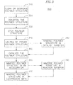
- the method also includes a task 300 of metallizing the one or more regions of the polymer structure 200 that are configured to accept electroless metal plating (e.g., the method may include a task of electroless metal plating the polymer optical waveguides 225 and the nodes 226 in the second region of the polymer structure 200 that are formed from the second photo-monomer 218 ).
- Suitable processes for metallizing polymers are described in ASTM Standard B727-04, 2009 , " Standard Practice for Preparation of Plastics Materials for Electroplating," ASTM International, West Conshohocken, PA, 2009, DOI: 10.1520/B0727-04R09 .
- the task 300 of metallizing the polymer structure 200 includes a task 310 of cleaning or degreasing the polymer structure 200 by any suitable process, such as, for instance, with a solvent rinse or a detergent/alkaline cleaner, to remove any surface contamination that would otherwise reduce the efficacy of subsequent tasks of the metallizing process.
- the task of metallizing the polymer structure 200 may also include a task of rinsing the polymer structure 200 with de-ionized water (DIW) to prevent cross-contamination.
- DIW de-ionized water
- the task 300 of metallizing regions of polymer structure 200 also includes a task 320 of conditioning the polymer structure 200 by any suitable process, such as, for instance, immersing the polymer structure 200 in either an acidic bath or an organic conditioning bath. Conditioning the polymer structure 200 is configured to prepare the polymer structure 200 for the next task 330 of etching the polymer structure 200.
- the task 330 of etching the polymer structure 200 includes immersing the polymer structure 200 in an etchant solution, such as a heated acidic oxidative solution (e.g., a mixture of chromic and sulfuric acid in DIW) or a basic oxidative chemical solution (e.g., potassium permanganate and sodium hydroxide in DIW).
- a heated acidic oxidative solution e.g., a mixture of chromic and sulfuric acid in DIW
- a basic oxidative chemical solution e.g., potassium permanganate and sodium hydroxide in DIW.
- the DIW may be used to control the concentration of the oxidative solution.
- the task 330 of etching the polymer structure 200 is configured to roughen the surfaces of the polymer optical waveguides 214, 225, 232 and thereby increase the surface area of the polymer optical waveguides 214, 225, 232.
- the increased surface area will allow for additional catalyst particles to form on the surfaces of the polymer optical waveguides 214, 225, 232 during a subsequent task of catalyzing the polymer structure.
- the additional catalyst particles formed on the polymer structure provide additional sites to initiate the plating reaction in the electroless bath.
- the task 300 of metallizing one or more regions of the polymer structure 200 includes a task 340 of neutralizing the etched polymer structure 200 by immersing the etched polymer structure 200 in a neutralizing solution that reduces the oxidizer (e.g., the heated acidic oxidative solution or the basic oxidative solution applied during the task 330 of etching the polymer structure 200 ) and neutralizes the pH.
- the task 300 of metallizing the polymer structure 200 may also include a task of rinsing the polymer structure 200 with DIW.
- the task 300 of metallizing one or more regions of the polymer structure 200 includes a task 350 of catalyzing the polymer structure 200.
- the catalyst is configured to catalyze the reaction necessary to deposit the plating metal (e.g., copper, nickel, palladium, gold, silver, zinc, cobalt, chromium, platinum, or iron) onto the surface of the polymer structure 200.
- the task 350 may also include agitating the catalyzing solution and flipping the polymer structure 200 one or more times during the task of immersing the etched polymer structure 200 in the catalyzing solution.
- the task 300 of metallizing the polymer structure 200 may also include a task of pretreating the etched polymer structure 200 before the task 350 of catalyzing the polymer structure 200.
- the task 300 of metallizing one or more regions of the polymer structure 200 also includes a task 360 of immersing the polymer structure 200 in an accelerator solution.
- This task 360 of immersing the polymer structure 200 in an accelerator is configured to remove any contaminants on the catalyst, which was deposited onto the surface of the polymer structure 200 during the task 350 of catalyzing the polymer structure 200. Removing the contamination from the catalyst surface is configured to accelerate the metal plating reaction at the activated sites during a task of immersing the polymer structure in an electroless bath, as described below.
- the task 300 of metallizing one or more regions of the polymer structure 200 includes a task 370 of immersing the polymer structure 200 in an electroless bath including a desired metal salt, a reducing agent, and additives to assist the plating reaction.
- the electroless bath may include any suitable metal salt depending on the desired plating metal (e.g., copper, nickel, palladium, gold, silver, zinc, cobalt, chromium, platinum, or iron).
- the plating process is triggered auto-catalytically on the activated sites on the surface of the polymer structure 200.
- the task 300 of metallizing the polymer structure 200 may also include a task of rinsing the plated polymer structure with DIW and then drying the plated polymer structure following the task 370 of immersing the polymer structure in the electroless bath. Additionally, in one embodiment, the task 300 of metallizing the polymer structure 200 may include a task of rinsing the polymer structure 200 in DIW following each of the above-referenced tasks 310-370 to prevent cross-contamination.
- the first photo-monomer 207 may be selected such that the polymer optical waveguides 214, 232 and the nodes 215, 216, 233 formed from the first photo-monomer 207 are configured to reject or inhibit metal plating during the task 300 of metallizing the polymer structure 200
- the second photo-monomer 218 may be selected such that the polymer optical waveguides 225 and the nodes 226 formed from the second photo-monomer 218 are configured to accept or receive metal plating during the task 300 of metallizing the polymer structure 200.
- photo-monomers may be suitable for rejecting or inhibiting electroless metal plating and these suitable photo-monomers may be configured to reject or inhibit metal plating from an electroless plating process in a variety of different manners (i.e., a variety of different chemical mechanisms and properties of the photo-monomer may be utilized to inhibit or reject electroless metal plating).
- a person of ordinary skill in the art will appreciate that any suitable photo-monomer composition may be selected depending on the desired receptivity or unreceptivity to metal plating of the polymer optical waveguides formed from the photo-monomer.
- the composition of the first photo-monomer may be selected such that the first photo-monomer 207 inherently interferes with one or more mechanisms of the electroless metal plating process.
- the first photo-monomer 207 may be selected such that the polymer optical waveguides 214, 232 and the nodes 215, 216, 233 formed from the first photo-monomer 207 prevent the reduction of the catalyst onto the surfaces of the polymer optical waveguides 214, 232 and the nodes 215, 216, 233 during the task 350 of catalyzing the polymer structure 200.
- Preventing the catalyst from reducing onto the polymer optical waveguides 214, 232 and the nodes 215, 216, 233 formed from the first photo-monomer 207 prevents the metal plating from depositing onto the polymer optical waveguides 214, 232 and the nodes 215, 216, 233 during the task 370 of immersing the polymer structure 200 in the electroless bath.
- the first photo-monomer 207 may be selected such that the polymer optical waveguides 214, 232 and the nodes 215, 216, 233 formed from the first photo-monomer 207 bind with the catalyst during the task 350 of catalyzing the polymer structure 200 such that the catalyst cannot catalyze the reduction of metal onto the polymer optical waveguides 214, 232 and the nodes 215, 216, 233 during the task 370 of immersing the polymer structure 200 in the electroless bath.
- the first photo-monomer 207 may be selected such that the polymer optical waveguides 214, 232 and the nodes 215, 216, 233 formed from the first photo-monomer 207 oxidize the reducing agent, bind with the reducing agent so that it cannot react, or bind with the metal so that it cannot be reduced onto the polymer optical waveguides 214, 232 and the nodes 215, 216, 233 during the task 370 of immersing the polymer structure 200 in the electroless bath.
- the task 300 of selectively metallizing one or more regions of the polymer structure 200 may include a task 380 of immersing the polymer structure 200 in a solution containing a catalyst inhibitor prior to the task 350 of catalyzing the polymer structure 200.
- the surfaces of the polymer structure 200 onto which the catalyst inhibitor is deposited are configured to inhibit or prevent the deposition of the catalyst during the task 350 of catalyzing the polymer structure 200.
- the first photo-monomer 207 may be selected such that the polymer optical waveguides 214, 232 and the nodes 215, 216, 233 formed from the first photo-monomer 207 attract the catalyst inhibitor (i.e., the catalyst inhibitor will be deposited onto the polymer optical waveguides 214, 232 and the nodes 215, 216, 233 formed from the first photo-monomer 207 ) and the second photo-monomer 218 may be selected such that the polymer optical waveguides 225 and the nodes 226 formed from the second photo-monomer 218 repel the catalyst inhibitor.
- the catalyst inhibitor i.e., the catalyst inhibitor will be deposited onto the polymer optical waveguides 214, 232 and the nodes 215, 216, 233 formed from the first photo-monomer 207
- the second photo-monomer 218 may be selected such that the polymer optical waveguides 225 and the nodes 226 formed from the second photo-monomer 218 repel the catalyst inhibitor.
- the catalyst will deposit only onto the polymer optical waveguides 225 and the nodes 226 that are formed from the second photo-monomer 218. Therefore, during the task 370 of immersing the polymer structure 200 in the electroless bath, the plating metal (e.g., copper, nickel, palladium, gold, silver, zinc, cobalt, chromium, platinum, or iron) will deposit only onto the polymer optical waveguides 225 and the nodes 226 that are formed from the second photo-monomer 218.
- the plating metal e.g., copper, nickel, palladium, gold, silver, zinc, cobalt, chromium, platinum, or iron
- any suitable catalyst inhibitor may be selected depending on the composition of the polymer structure and the chemical composition of the catalyst selected. This method of selectively plating regions of the polymer structure 200 is referred to herein as the "catalyst poisoning" method.
- the task 300 of selectively metallizing one or more regions of the polymer structure 200 may include a task 390 of immersing the polymer structure 200 in a solution containing a reaction inhibitor prior to the task 370 of immersing the polymer structure 200 in the electroless bath.
- the surfaces of the polymer structure 200 onto which the reaction inhibitor is deposited are configured to inhibit or prevent the deposition of the plating metal during the task 370 of immersing the polymer structure 200 in the electroless bath.
- the first photo-monomer 207 may be selected such that the polymer optical waveguides 214, 232 and the nodes 215, 216, 233 formed from the first photo-monomer 207 attract the reaction inhibitor (i.e., the reaction inhibitor will be deposited onto the polymer optical waveguides 214, 232 and the nodes 215, 216, 233 formed from the first photo-monomer 207 ) and the second photo-monomer 218 may be selected such that the polymer optical waveguides 225 and the nodes 226 formed from the second photo-monomer 218 repel the reaction inhibitor.
- the reaction inhibitor i.e., the reaction inhibitor will be deposited onto the polymer optical waveguides 214, 232 and the nodes 215, 216, 233 formed from the first photo-monomer 207
- the second photo-monomer 218 may be selected such that the polymer optical waveguides 225 and the nodes 226 formed from the second photo-monomer 218 repel the reaction inhibitor.
- the plating metal e.g., copper, nickel, palladium, gold, silver, zinc, cobalt, chromium, platinum, or iron
- the plating metal will deposit only onto the polymer optical waveguides 225 and the nodes 226 that are formed from the second photo-monomer 218 (i.e., the polymer optical waveguides 225 and the nodes 226 of the polymer structure 200 that do not contain the reaction inhibitor).
- This method of selectively plating regions of the polymer structure 200 is referred to herein as the "inhibition of metal reaction" method.
- the first and second photo-monomers 207, 218 may be selected such that the polymer optical waveguides 214, 232 and the nodes 215, 216, 233 formed from the first photo-monomer 207 are configured to etch at a faster rate than the polymer optical waveguides 225 and the nodes 226 formed from the second photo-monomer 218 during the task 330 of etching the polymer structure 200.
- This disparity in etching rates permits the polymer optical waveguides 225 and the nodes 226 formed from the second photo-monomer 218 to be suitably/properly etched and the polymer optical waveguides 214, 232 and the nodes 215, 216, 233 formed from the first photo-monomer 207 to be over-etched during the task 350 of etching the polymer structure 200.
- the properly etched polymer optical waveguides 225 and nodes 226 formed from the second photo-monomer 218 are configured to accept catalyst deposition (e.g., the suitably etched polymer optical waveguides 225 and nodes 226 will have the necessary surface roughness and surface energy to allow catalyzation to occur).
- the over-etched polymer optical waveguides 214, 232 and nodes 215, 216, 233 formed from the first photo-monomer 207 are configured to inhibit or prevent proper catalyst deposition during the task 350 of catalyzing the polymer structure 200 (e.g., the excess roughness of the over-etched polymer optical waveguides 214, 232 and nodes 215, 216, 233 may prevent proper catalyst deposition).
- the plating metal e.g., copper, nickel, palladium, gold, silver, zinc, cobalt, chromium, platinum, or iron
- the plating metal will deposit only onto the polymer optical waveguides 225 and the nodes 226 that are formed from the second photo-monomer 218.
- This method of selectively plating regions of the polymer structure 200 is referred to herein as the "over-etched polymer surface" method.
- the first and second photo-monomers 207, 218 may be selected such that the polymer optical waveguides 214, 232 and the nodes 215, 216, 233 formed from the first photo-monomer 207 are configured to etch at a faster rate than the polymer optical waveguides 225 and the nodes 226 formed from the second photo-monomer 218, which permits the polymer optical waveguides 225 and the nodes 226 formed from the second photo-monomer 218 to be suitably etched and the polymer optical waveguides 214, 232 and the nodes 215, 216, 233 formed from the first photo-monomer 207 to be over-etched during the task 330 of etching the polymer structure 200.
- the increased etching of the polymer optical waveguides 214, 232 and the nodes 215, 216, 233 formed from the first photo-monomer 207 may not completely inhibit the deposition of the catalyst onto the over-etched polymer optical waveguides 214, 232 and nodes 215, 216, 233. Instead, the increased etching of the polymer optical waveguides 214, 232 and the nodes 215, 216, 233 formed from the first photo-monomer 207 may permit a reduced or limited amount of catalyst to be deposited onto the surface of the over-etched polymer optical waveguides 214, 232 and nodes 215, 216, 233.
- the plating metal will deposit onto the surfaces of the over-etched polymer optical waveguides 214, 232 and nodes 215, 216, 233, but the bond between the plating metal and the surface of the over-etched polymer optical waveguides 214, 232 and nodes 215, 216, 233 will be sufficiently weak or poor such that the metal plating may be readily removed.
- the method 300 of partially metallizing the polymer structure 200 may include removing the metal plating on the over-etched polymer optical waveguides 214, 232 and nodes 215, 216, 233 by any suitable process, such as, for instance, by etching or with abrasive techniques using pressurized fluids, such as air, nitrogen, or water.
- bonds between the metal plating and the suitably etched polymer optical waveguides 225 and nodes 226 formed from the second photo-monomer 218 are suitably strong such that the metal plating on the suitably etched polymer optical waveguides 225 and nodes 226 will not be removed during the task of removing the metal plating on the over-etched polymer optical waveguides 214, 232 and nodes 215, 216, 233.
- This method of selectively plating regions of the polymer structure 200 is referred to herein as the "increased etch rate- post process" method.
- first and second photo-monomers 207, 218 may be selected such that the second photo-monomer 218 is configured to polymerize faster than the first photo-monomer 207.
- the second photo-monomer 218 may be configured to polymerize at a different wavelength (i.e., a different polymerization initiation wavelength) of light than the first photo-monomer 207.
- the polymer optical waveguides 225 formed from the second photo-monomer 218 will form faster than the polymer optical waveguides 214, 232 formed from the first photo-monomer.
- the polymer optical waveguides 225 formed from the second photo-monomer 218 will fully cure (i.e., the functional groups will be fully cross-linked), but the polymer optical waveguides 214, 232 formed from the first photo-monomer 207 will remain partially cured (i.e., the functional groups will be partially cross-linked) due to the slower polymerization rate or the different polymerization initiation wavelength of the second photo-monomer 218.
- light e.g., UV light
- the fully cured, cross-linked polymer optical waveguides 225 are configured to accept electroless metal plating and the partially cured polymer optical waveguides 214, 232 are configured to reject electroless metal plating. Accordingly, during the task 370 of immersing the polymer structure 200 in the electroless bath, the plating metal (e.g., copper, nickel, palladium, gold, silver, zinc, cobalt, chromium, platinum, or iron) will deposit only onto the fully cured polymer optical waveguides 225 formed from the second photo-monomer 218.
- the plating metal e.g., copper, nickel, palladium, gold, silver, zinc, cobalt, chromium, platinum, or iron
- the difference in polymerization rate or polymerization initiation wavelength between the first and second photo-monomers 207, 218 enables selectivity over which portions or regions of the polymer structure 200 will metallize.
- This method of selectively plating regions of the polymer structure 200 is referred to herein as the "uncured surface inhibition of plating" method.
- the partially cured polymer optical waveguides 214, 232 are configured to etch at a faster rate than the fully cured polymer optical waveguides 225 during the task 330 of etching the polymer structure 200.
- the "uncured surface inhibition of plating" method may be used in conjunction with the "over-etched polymer surface” method or the "increased etch rate- post process” method described above to partially metallize the polymer structure 200.
- the second photo-monomer 218 may be selected such that the polymer optical waveguides 225 and the nodes 226 formed from the second photo-monomer 218 are configured to etch at a suitable rate
- the first photo-monomer 207 may be selected such that the polymer optical waveguides 214, 232 and the nodes 215, 216, 233 formed from the first photo-monomer 207 are configured not to etch during the task 330 of etching the polymer structure 200.
- the increased surface roughness of the etched polymer optical waveguides 225 and nodes 226 increases the surface area of the polymer optical waveguides 225 and the nodes 226 and thereby allows additional catalyst particles to deposit onto the surface of the polymer optical waveguides 225 and the nodes 226 during the task 350 of catalyzing the polymer structure 200.
- the additional catalytic particles deposited onto the surface of the etched the polymer optical waveguides 225 and nodes 226 trigger the metal plating process during the task 370 of immersing the polymer structure 200 in the electroless bath.
- the un-etched polymer optical waveguides 214, 232 and nodes 215, 216, 233 formed from the first photo-monomer 207 are not configured to accept proper catalyst deposition during the task 350 of catalyzing the polymer structure 200 (i.e., the insufficient surface roughness of the un-etched polymer optical waveguides 214, 232 and nodes 215, 216, 233 prevents proper catalyst deposition onto the un-etched polymer optical waveguides 214, 232 and nodes 215, 216, 233).
- the plating metal e.g., copper, nickel, palladium, gold, silver, zinc, cobalt, chromium, platinum, or iron
- the plating metal will deposit only onto the polymer optical waveguides 225 and the nodes 226, which are formed from the second photo-monomer 218.
- This method of selectively plating regions of the polymer structure 200 is referred to herein as the "etch resistant polymer- prevention of catalyst deposition" method.
- the method may also include a task of selectively removing at least a portion of the polymer optical waveguides following the task 300 of selectively metallizing one or more regions of the polymer structure 200.
- the polymer optical waveguides 214, 225, 232 may be removed by any suitable process, such as, for instance, by chemically etching the polymer optical waveguides 214, 225, 232.
- Selectively removing the polymer optical waveguides 214, 225, 232 leaves a plurality of hollow tubular struts 234 formed out of the metal plating 235 previously deposited onto the polymer optical waveguides 214, 225, 232 during the task 300 of selectively metallizing one or more regions of the polymer structure 200.
- the hollow tubular struts 234 will be interconnected following the task of removing the polymer optical waveguides 214, 225, 232.
- the method also includes a task of applying a coating 237 (e.g., a metallic or polymer coating) to the entire polymer structure 200 prior to the task of removing the polymer optical waveguides 214, 225, 232.
- a coating 237 e.g., a metallic or polymer coating
- the hollow tubular struts 234 will be thinner in the regions of the polymer structure 200 that rejected metal plating and relatively thicker in the regions where the polymer structure 200 accepted the metal plating 235 (e.g., as illustrated in FIG. 4 , the hollow tubular struts 234 may be thicker around the nodes 236 because the nodes 236 are coated by the metal plating 235 as well as the coating 237 ).
- the coating 237 may be applied to the polymer structure 200 by any suitable process, such as, for instance, chemical vapor deposition, sputtering, electro-plating, or electroless plating.
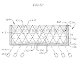
- the method includes a task of filling at least a portion of a reservoir 401 with a volume of a first photo-monomer 402.
- the reservoir 401 is defined by a mold 403 having a translucent base 404 and a rim 405 extending up from a periphery of the base 404.
- the method also includes a task of covering the translucent base 404 of the mold 403 with a mask 406 defining a plurality of apertures 407.
- the height h 1 to which the first photo-monomer 402 is filled in the reservoir 401 may be selected depending on the desired size and configuration of the region of the polymer structure 400 that is configured to accept or reject electroless plating.
- the method also includes a task of irradiating the volume of the first photo-monomer 402 by directing a plurality of light beams 408 (e.g., collimated or substantially collimated UV light beams) from one or more light sources 409 up through the apertures 407 in the mask 406 and through the translucent base 404 of the mold 403. Regions of the first photo-monomer 402 that are exposed to the light beams 408 cure (i.e., polymerize) to form a plurality of polymer optical waveguides 410 in a first region of the polymer structure 400.
- a plurality of light beams 408 e.g., collimated or substantially collimated UV light beams
- the polymer optical waveguides 410 in the first region of the polymer structure 400 are polymerized into a unitary structure, although in one or more alternate embodiments, the polymer optical waveguides 410 may be discrete segments.
- the light sources 409 may be oriented and positioned based on the desired configuration of the polymer optical waveguides 410 in the first region of the polymer structure 400.
- the method also includes a task of removing the unpolymerized volume of the first photo-monomer 402 from the reservoir 401 and filling the reservoir 401 with a second photo-monomer 411.
- the volume of the second photo-monomer 411 is filled to a height h 2 in the reservoir 401 such that an upper surface 412 of the second photo-monomer 411 is above the polymer optical waveguides 410 formed from the first photo-monomer 402 (i.e., the volume of the second photo-monomer 411 is greater than the volume of the first photo-monomer 402 such that the polymer optical waveguides 410 formed from the first photo-monomer 402 are completely submerged in the second photo-monomer 411 ).
- the method also includes a task of directing a plurality of light beams 413 (e.g., collimated or substantially collimated UV light beams) from the light sources 409 through the apertures 407 in the mask 406 and into the second photo-monomer 411. Additionally, in the illustrated embodiment, the light beams 413 are directed through the second photo-monomer 411 at the same angles that the light beams 408 were directed through the first photo-monomer 402.
- a plurality of light beams 413 e.g., collimated or substantially collimated UV light beams
- the light beams 413 are directed through the polymer optical waveguides 410 formed from the first photo-monomer 402 such that polymer optical waveguides 414 grow or extend up from upper ends 415 of the polymer optical waveguides 410 and into the second photo-monomer 411 (e.g., the light beams 413 pass through the polymer optical waveguides 410 formed from the first photo-monomer 402 and extend into the second photo-monomer 411 to form polymer optical waveguides 414 extending upwards from upper ends 415 of the polymer optical waveguides 410 formed from the first photo-monomer 402 ).
- the polymer optical waveguides 414 extend or grow sufficiently into the second photo-monomer 411 such that the polymer optical waveguides 414 are polymerized together into a unitary, lattice structure.
- the height h 2 to which the second photo-monomer 411 is filled in the reservoir 401 may be selected such that the polymer optical waveguides 414 formed from the second photo-monomer 411 are discrete, separate segments.
- the method may also include a task of removing the unpolymerized volume of the second photo-monomer 411 from the reservoir 401 and filling the reservoir 401 with a third photo-monomer 416.
- the third photo-monomer 416 may be the same as or similar to the first photo-monomer 402, although in one or more alternate embodiments, the third photo-monomer 416 may be different than the first photo-monomer 402.
- the third photo-monomer 416 is filled to a height h 3 in the reservoir 401 such that an upper surface 417 of the third photo-monomer 416 is above upper ends 418 the polymer optical waveguides 414 formed from the second photo-monomer 411.
- the method also includes a task of irradiating the third photo-monomer 416 by directing a plurality of light beams 419 (e.g., collimated or substantially collimated UV light beams) from the light sources 409 up through the apertures 407 in the mask 406.
- a plurality of light beams 419 e.g., collimated or substantially collimated UV light beams
- the light beams 419 are directed through the third photo-monomer 416 at the same angles that the light beams 413 were directed through the second photo-monomer 411 such that polymer optical waveguides 420 grow or extend up into the third photo-monomer 416 (e.g., the light beams 419 pass through the polymer optical waveguides 414 formed from the second photo-monomer 411 and extend into the third photo-monomer 416 to form polymer optical waveguides 420 extending upwards from upper ends 418 of the polymer optical waveguides 414 formed from the second photo-monomer 411 ).
- the polymer optical waveguides 420 extend or grow sufficiently into the third photo-monomer 416 such that the polymer optical waveguides 420 are polymerized together into a unitary, lattice structure.
- the height h 3 to which the third photo-monomer 416 is filled in the reservoir 401 may be selected such that the polymer optical waveguides 420 formed from the third photo-monomer 416 are discrete, separate segments.
- the above-described tasks of filling the reservoir 401 with a first photo-monomer 402, directing a plurality of light beams 408 into the first photo-monomer 402, filling the reservoir 401 with a second photo-monomer 411 to submerge the polymer optical waveguides 410 formed from the first photo-monomer 402 in the second photo-monomer 411, and directing a plurality of light beams 413 through the polymer optical waveguides 410 formed from the first photo-monomer 402 and into the second photo-monomer 411 may be repeated any suitable number of times depending on the desired thickness of the polymer structure 400 and the number of layers or regions of the polymer structure 400 that are formed from the different photo-monomers.
- one or more of the photo-monomers 402, 411, 416 may be selected such that the polymer optical waveguides 410, 414, and/or 420 formed from those photo-monomers 402, 411, or 416 are receptive to metal plating and one or more of the photo-monomers 402, 411, 416 may be selected such that the polymer optical waveguides 410, 414, and/or 420 formed from those photo-monomers 402, 411, or 416 are configured to reject or inhibit metal plating (i.e., the polymer structure 400 formed from the above-described tasks will have one or regions or layers formed from a polymer material receptive to electroless plating and one or more regions or layers formed from a polymer configured to reject or inhibit electroless plating).
- each volume of photo-monomer 402, 411, 416 in the reservoir 401 may be varied depending upon the desired thicknesses of the layers or regions of the polymer structure 400 that are receptive to electroless plating and the desired thicknesses of the layers or regions of the polymer structure 400 that are configured to reject or inhibit electroless plating.
- Regions of the polymer structure 400 that are receptive to metal plating may then be selectively plated according any one of the processes described above, including the "catalyst poisoning” method, the “inhibition of metal reaction” method, the “over-etched polymer surface” method, the “increased etch rate- post process” method, the “uncured surface inhibition of plating” method, or the “etch resistant polymer- prevention of catalyst deposition” method.
- the method includes filling at least a portion of a reservoir 501 with a volume of a first photo-monomer 502 and layering a volume of a second photo-monomer 503 on top of the first photo-monomer 502.
- the reservoir 501 is defined by a mold 504 having a translucent base 505 and a rim 506 extending up from a periphery of the base 505.
- the method also includes a task of covering the translucent base 505 of the reservoir 501 with a mask 507 defining a plurality of apertures 508.
- the first and second photo-monomers 502, 503 are immiscible photo-monomers such that the first and second photo-monomers 502, 503 remain in separate layers and do not mix or substantially do not mix.
- the first and second photo-monomers 502, 503 are also configured such that they possess an identical or equivalent index of refraction, the significance of which is described below.
- the method includes filling the reservoir 501 with two layers of photo-monomers 502, 503, in one or more alternate embodiments, the method may include tasks of filling the reservoir 501 with any other suitable number of layers of photo-monomers, such as for instance, from three to ten layers, depending on the desired regions or layers of the polymer structure 500 that are configured to reject or inhibit metal plating and the desired regions or layers of the polymer structure 500 that are configured to accept metal plating.
- the first and second layers of the photo-monomers 502, 503 may have any suitable thicknesses t 1 , t 2 , respectively, depending on the desired upon the desired thickness of the layer or region of the polymer structure 500 that is receptive to electroless plating and the desired thickness of the layer or region of the polymer structure 500 that is configured to reject or inhibit electroless plating. Additionally, in an alternate embodiment, the method may also include filling the reservoir 501 with more than two different types or kinds of photo-monomer, such as, for instance, three or more different photo-monomers.
- the method also includes a task of irradiating the first and second photo-monomer layers 502, 503.
- the task of irradiating the first and second photo-monomer layers 502, 503 includes directing a plurality of light beams 509 (e.g., collimated or substantially collimated UV light beams) from one or more light sources 510 up through the apertures 508 in the mask 507, through the translucent base 505 of the mold 504, and up into the first and second photo-monomer layers 502, 503.
- a plurality of light beams 509 e.g., collimated or substantially collimated UV light beams
- Regions of the first and second photo-monomer layers 502, 503 that are exposed to the light beams 509 cure (i.e., polymerize) to form a plurality of polymer optical waveguides 511, 512, respectively. Accordingly, the polymer optical waveguides 511, 512 grow or extend up through the first and second photo-monomer layers 502, 503 (e.g., the light beams 509 pass through the first photo-monomer 502 to form polymer optical waveguides 511 and extend into the second photo-monomer 503 to form polymer optical waveguides 512 extending upwards from upper ends of the polymer optical waveguides 511 formed from the first photo-monomer 502 ).
- the polymer optical waveguides 511, 512 have the same orientation across the dissimilar first and second photo-monomers 502, 503.
- the polymer optical waveguides 511, 512 are polymerized together into a unitary, lattice structure.
- the composition of either the first photo-monomer 502 or the second photo-monomer 503 may be selected such that the polymer optical waveguides 511, 512 formed from that photo-monomer 502 or 503 are receptive to metal plating and the composition of the other photo-monomer 502, 503 may be selected such that the polymer optical waveguides 511, 512 formed from that photo-monomer 502 or 503 are configured to reject or inhibit metal plating.
- the polymer structure 500 formed from the above-described tasks will have one or regions or layers formed from a polymer material receptive to electroless plating and one or more regions or layers formed from a polymer configured to reject or inhibit electroless plating.
- each volume of photo-monomer 502, 503 in the reservoir 501 may be varied depending upon the desired thicknesses of the layers or regions of the polymer structure 500 that are receptive to electroless plating and the desired thicknesses of the layers or regions of the polymer structure 500 that are configured to reject or inhibit electroless plating.
- Regions of the polymer structure 500 that are receptive to metal plating may then be selectively plated according any one of the processes described above, including the "catalyst poisoning” method, the “inhibition of metal reaction” method, the “over-etched polymer surface” method, the “increased etch rate- post process” method, the “uncured surface inhibition of plating” method, or the “etch resistant polymer- prevention of catalyst deposition” method.
- the method includes a task of at least partially filling a reservoir 601 with a volume of a first photo-monomer 602.
- the reservoir 601 is defined by a mold 603 having a translucent base 604 and a rim 605 extending up from a periphery of the base 604.
- the method also includes a task of covering the translucent base 604 of the reservoir 601 with a mask 606 defining a plurality of apertures 607.
- the method also includes a task of irradiating the first photo-monomer 602 by directing a plurality of light beams 608 (e.g., collimated or substantially collimated UV light beams) from one or more light sources 609 up through the apertures 607 in the mask 606, through the translucent base 604 of the mold 603, and up into the first photo-monomer 602.
- a plurality of light beams 608 e.g., collimated or substantially collimated UV light beams
- regions of the first photo-monomer 602 that are exposed to the light beams 608 cure (i.e., polymerize) to form a plurality of polymer optical waveguides 610.
- the polymer optical waveguides 610 are polymerized together into a unitary, lattice structure.
- the method also includes a task of removing the unpolymerized volume of the first photo-monomer 602 from the reservoir 601 and filling at least a portion of the reservoir 601 with a second photo-monomer 611.
- the second photo-monomer 611 is filled to a height h in the reservoir 601 such that an upper surface 612 of the second photo-monomer is below upper ends 613 of the polymer optical waveguides 610 formed from the first photo-monomer 602 (i.e., the polymer optical waveguides 610 formed from the first photo-monomer 602 are only partially submerged in the second photo-monomer 611).
- the second photo-monomer 611 may be filled to any other suitable height h in the reservoir 601.
- the second photo-monomer 611 may be filled to a height h such that the upper surface 612 of the second photo-monomer 611 is substantially flush or level with the upper ends 613 of the polymer optical waveguides 610 formed from the first photo-monomer 602.
- the second photo-monomer 611 may be filled to a height h in the reservoir 601 such that the upper surface 612 of the second photo-monomer 611 is above the upper ends 613 of the polymer optical waveguides 610 formed from the first photo-monomer 602.
- the method also includes a task of irradiating the second photo-monomer 611 by directing a plurality of light beams 614 through the apertures 607 defined in the mask 606. Additionally, in the illustrated embodiment, the light beams 614 are directed through the second photo-monomer 611 at the same angles that the light beams 608 were directed through the first photo-monomer 602. Accordingly, in the illustrated embodiment, the light beams 614 are directed through at least a portion of the polymer optical waveguides 610 formed from the first photo-monomer 602.
- effluence of the light beams 614 directed through the polymer optical waveguides 610 causes the portions of the polymer optical waveguides 610 submerged in the second photo-monomer 611 to grow outward into the second photo-monomer 611 (e.g., the polymer optical waveguides 610 submerged in the second photo-monomer 611 may grow radially outward into the second photo-monomer 611 ).
- thin-walled polymer shells 615 formed from the second photo-monomer 611 will form around the portions of the polymer optical waveguides 610 submerged in the second photo-monomer 611 (i.e., the polymer optical waveguides 610 formed from the first photo-monomer 602 will define solid cores surrounded by the thin-walled polymer shells 615 formed from the second photo-monomer 611).
- the method includes directing the light beams 614 through the polymer optical waveguides 610 for a sufficient duration to achieve the desired thickness of the thin-walled polymer shells 615 formed from the second photo-monomer 611.
- the composition of either the first photo-monomer 602 or the second photo-monomer 611 may be selected such that the polymer optical waveguides 610 or the thin-walled polymer shells 615 formed from that photo-monomer 602 or 611 are receptive to metal plating and the composition of the other photo-monomer 602, 611 may be selected such that the polymer optical waveguides 610 or the thin-walled polymer shells 615 formed from that photo-monomer 602 or 611 are configured to reject or inhibit metal plating.
- the polymer structure 600 formed from the above-described tasks will have one or regions formed from a polymer material receptive to electroless plating and one or more regions formed from a polymer configured to reject or inhibit electroless plating.
- the height h of the volume of the second photo-monomer 611 in the reservoir 601 may be varied depending upon the desired thickness of the region of the polymer structure 600 that is receptive to electroless plating and the desired thickness of the region of the polymer structure 600 that is configured to reject or inhibit electroless plating. Regions of the polymer structure 600 that are receptive to metal plating may then be selectively plated according any one of the processes described above, including the "catalyst poisoning" method, the "inhibition of metal reaction” method, the "over-etched polymer surface” method, the “increased etch rate-post process” method, the "uncured surface inhibition of plating” method, or the "etch resistant polymer- prevention of catalyst deposition” method.
- the method includes a task of at least partially filling a reservoir 701 with a volume of a photo-monomer 702.
- the reservoir 701 is defined by a mold 703 having a translucent base 704 and a rim 705 extending up from a periphery of the base 704.
- the method also includes a task of covering the translucent base 704 of the mold 703 with a mask 706 defining a plurality of apertures 707.
- the method also includes a task of irradiating the photo-monomer by directing a plurality of light beams 708 (e.g., collimated or substantially collimated UV light beams) from one or more light sources 709 up through the apertures 707 in the mask 706, through the translucent base 704 of the mold 703, and up into the photo-monomer 702.
- regions of the photo-monomer 702 that are exposed to the light beams 708 cure (i.e., polymerize) to form a plurality of polymer optical waveguides 710.
- the polymer optical waveguides 710 intersect each other and are polymerized together into a unitary, lattice structure. Additionally, the polymer optical waveguides 710 of the lattice structure are in a partially cured state following the task of irradiating the photo-monomer 702 with the plurality of light beams 708.
- the method also includes a task of post-curing regions or portions of the partially cured polymer structure 711.
- the task of post-curing regions of the polymer structure 711 includes a task of removing the partially-cured polymer lattice structure 711 from the reservoir 701 and covering an upper end of the partially-cured polymer structure 711 with a mask 712 defining a plurality of apertures 713.
- the task of post-curing regions of the partially-cured polymer structure 711 also includes irradiating at least a portion of the partially-cured polymer structure 711 with a plurality of light beams 714 (e.g., UV light beams) from one or more light sources 717 directed through the apertures 713 in the mask 712.
- Irradiating the partially-cured polymer structure 711 is configured to fully cure those portions or regions 715 of the polymer structure 711 that are exposed to the lights beams 714 (i.e., the portions or regions 715 of the partially-cured polymer structure 711 that are exposed to the light beams 714 become fully cured and cross-linked).
- the light beams 714 are oriented directly down through the apertures 713 in the mask 712 (e.g., perpendicular or substantially perpendicular to the mask 712 ) such that the fully-cured regions 715 of the polymer structure 700 are vertical columns.
- the light beams 714 may be directed through the apertures 713 in the mask 712 at any other suitable angles, such as, for instance, from approximately 15 degrees to approximately 60 degrees, depending on the desired orientation of the fully-cured regions 715 of the polymer structure 700.
- the method may also include directing the light beams 714 through the apertures 713 in the mask 712 at more than one angle.
- the apertures 713 in the mask 712 may have any suitable shape, size, arrangement, and spacing depending upon the desired shape, size, arrangement, and spacing of the fully cured regions 715 of the polymer structure 700. Portions or regions 716 of the polymer structure 700 that are not exposed to the light beams 714 remain partially cured.
- the task of post-curing regions of the partially-cured polymer structure 711 may be performed while the partially-cured polymer structure 711 remains in the mold 703.
- the task of post-curing regions of the partially-cured polymer structure 711 may include draining the unpolymerized photo-monomer from the reservoir 701 after irradiating the photo-monomer 702 with the plurality of light beams 708, covering the upper end of the partially-cured polymer structure 711 with the mask 712, and irradiating the partially-cured polymer structure 711 with the plurality of light beams 714 to fully cure the exposed regions 716 of the polymer structure 711 while the polymer structure 711 remains in the mold 703.
- the polymer structure 700 formed from the above-described tasks will have one or more fully-cured (i.e., fully cross-linked) portions or regions 715 and one or more partially-cured portions or regions 716.
- the fully-cured regions 715 of the polymer structure 700 are configured to accept electroless metal plating and the partially-cured regions 716 of the polymer structure 700 are configured to prevent or inhibit electroless metal plating. Regions of the polymer structure 700 that are receptive to metal plating may then be selectively plated according any suitable process, such as, for instance, by performing the tasks illustrated in FIG. 3 .
- the selectively metallized structures of the present disclosure may be manufactured by any other suitable processes, such as, for instance, an additive manufacturing process (e.g., stereolithography, digital light processing, fused deposition, and/or selective laser sintering). Additionally, other suitable methods of manufacturing polymer structures for use with the methods of partially metallizing polymer structures of the present disclosure are described in U.S. Patent Application entitled “Multi-Chemistry Microlattice Structures and Methods of Manufacturing the Same", Attorney Docket No. H611:74327, filed on August 18, 2014.
Landscapes
- Physics & Mathematics (AREA)
- Optics & Photonics (AREA)
- General Physics & Mathematics (AREA)
- Engineering & Computer Science (AREA)
- Microelectronics & Electronic Packaging (AREA)
- Chemical & Material Sciences (AREA)
- Optical Integrated Circuits (AREA)
- General Chemical & Material Sciences (AREA)
- Chemical Kinetics & Catalysis (AREA)
- Materials Engineering (AREA)
- Mechanical Engineering (AREA)
- Metallurgy (AREA)
- Organic Chemistry (AREA)
- Chemically Coating (AREA)
- Optical Couplings Of Light Guides (AREA)
- Inorganic Chemistry (AREA)
- Health & Medical Sciences (AREA)
- Toxicology (AREA)
Claims (15)
- Verfahren zur Herstellung einer Struktur mit mindestens einem metallisierten Bereich und mindestens einem nicht metallisierten Bereich, wobei das Verfahren Folgendes umfasst:Aufbringen eines Metalls auf eine Polymer-Struktur mit einem ersten Bereich, der das Metall akzeptiert, und einem zweiten Bereich, der unempfänglich für das Metall ist,dadurch gekennzeichnet, dassder erste Bereich vollständig ausgehärtete, vernetzte Polymer-Lichtwellenleiter umfasst, und der zweite Bereich teilweise ausgehärtete Polymer-Lichtwellenleiter umfasst.
- Verfahren nach Anspruch 1, wobei das Metallisieren der Polymer-Struktur Folgendes umfasst:Konditionieren der Polymer-Struktur;Ätzen der Polymer-Struktur;Neutralisieren der Polymer-Struktur;Katalysieren der Polymer-Struktur;Eintauchen der Polymer-Struktur in einen Beschleuniger; undEintauchen der Polymer-Struktur in ein stromloses Bad.
- Verfahren nach Anspruch 1 oder Anspruch 2, wobei das Metallisieren der Polymer-Struktur ein Verfahren umfasst, das ausgewählt ist aus der Gruppe von Verfahren bestehend aus einem Verfahren der Katalysatorvergiftung, einem Verfahren der Hemmung der Reaktion des Metalls, einem Verfahren der überätzten Polymeroberfläche, einem Verfahren eines der erhöhten Ätzrate nachfolgenden Prozesses, einem Verfahren der Hemmung der Metallisierung einer nicht ausgehärteten Oberfläche, einem Verfahren der Verhinderung der Katalysatorabscheidung durch ein ätzresistentes Polymer, und Kombinationen davon.
- Verfahren nach Anspruch 1, ferner umfassend:Bestrahlen eines Volumens eines Photomonomers mit einer Mehrzahl von Lichtstrahlen, um die teilweise ausgehärteten Polymer-Lichtwellenleiter zu bilden; undBestrahlen von Bereichen der teilweise ausgehärteten Polymer-Lichtwellenleiter mit Lichtstrahlen, um die vollständig ausgehärteten, vernetzten Polymer-Lichtwellenleiter zu bilden.
- Verfahren nach einem der Ansprüche 1-3, wobei der erste Bereich eine erste Polymerzusammensetzung umfasst, und der zweite Bereich eine zweite Polymerzusammensetzung, die anders als die erste Polymerzusammensetzung ist, umfasst.
- Verfahren nach einem der Ansprüche 1-3 oder 5, ferner umfassend das Eintauchen der Polymer-Struktur in einen Katalysatorinhibitor, wobei sich der Katalysatorinhibitor auf dem zweiten Bereich der Polymer-Struktur abscheidet und der erste Bereich der Polymer-Struktur den Katalysatorinhibitor abweist.
- Verfahren nach einem der Ansprüche 1-3 oder 5, ferner umfassend das Eintauchen der Polymer-Struktur in einen Reaktionsinhibitor, wobei sich der Reaktionsinhibitor auf dem zweiten Bereich der Polymer-Struktur abscheidet und der erste Bereich der Polymer-Struktur den Reaktionsinhibitor abweist.
- Verfahren nach einem der Ansprüche 1-3 oder 5, ferner umfassend das Ätzen der Polymer-Struktur, wobei der erste Bereich der Polymer-Struktur mit einer ersten Rate ätzt und der zweite Bereich der Polymer-Struktur mit einer zweiten Rate, die anders als die erste Rate ist, ätzt.
- Verfahren nach einem der Ansprüche 1-3 oder 5-8, ferner umfassend das Ausbilden der Polymer-Struktur durch Bestrahlen eines oder mehrerer Photomonomere mit einer Mehrzahl von Lichtstrahlen, wobei die Polymer-Struktur eine in einer einheitlichen Gitterstruktur angeordnete Mehrzahl von miteinander verbundenen Polymer-Lichtwellenleitern umfasst.
- Verfahren nach einem der Ansprüche 1-3 oder 6-8, ferner umfassend das Ausbilden der Polymer-Struktur durch Bestrahlen eines Volumens eines ersten Photomonomers mit einer Mehrzahl von Lichtstrahlen, um den ersten Bereich der Polymer-Struktur auszubilden, und Bestrahlen eines Volumens eines zweiten Photomonomers mit einer Mehrzahl von Lichtstrahlen, um den zweiten Bereich der Polymer-Struktur auszubilden, wobei das zweite Photomonomer anders als das erste Photomonomer ist.
- Verfahren nach einem der Ansprüche 1-3 oder 6-8, ferner umfassend das Ausbilden der Polymer-Struktur durch ein Verfahren der additiven Fertigung, ausgewählt aus der Gruppe von Verfahren bestehend aus Stereolithographie, Digital Light Processing, Schmelzschichtung und selektivem Lasersintern.
- Verfahren nach Anspruch 10, ferner umfassend:Herausheben des ersten Bereichs der Polymer-Struktur aus einem Reservoir, das ein nicht polymerisiertes Volumen des ersten Photomonomers enthält;Füllen des Reservoirs mit dem zweiten Photomonomer; undSenken des ersten Bereichs der Polymer-Struktur in das Reservoir zum Inkontaktbringen mit dem zweiten Photomonomer vor dem Bestrahlen des zweiten Photomonomers mit den Lichtstrahlen.
- Verfahren nach Anspruch 10, ferner umfassend:Entfernen eines nicht polymerisierten Volumens des ersten Photomonomers aus einem Reservoir, das den ersten Bereich der Polymer-Struktur enthält;Füllen des Reservoirs mit dem zweiten Photomonomer bis zu einer Höhe, die größer als eine Höhe des ersten Bereichs der Polymer-Struktur ist; undwobei das Bestrahlen des zweiten Photomonomers das derartige Lenken der Lichtstrahlen durch den ersten Bereich der Polymer-Struktur, dass sich der zweite Bereich der Polymer-Struktur von einem oberen Ende des ersten Bereichs der Polymer-Struktur nach oben erstreckt, umfasst.
- Verfahren nach Anspruch 10, ferner umfassend:Entfernen eines nicht polymerisierten Volumens des ersten Photomonomers aus einem Reservoir, das den ersten Bereich der Polymer-Struktur enthält;Füllen des Reservoirs mit dem zweiten Photomonomer derart, dass zumindest ein Teil des ersten Bereichs der Polymer-Struktur in das zweite Photomonomer eingetaucht ist; undwobei das Bestrahlen des zweiten Photomonomers das Lenken der Lichtstrahlen durch den ersten Bereich der Polymer-Struktur zum Ausbilden einer Mehrzahl von dünnen Polymer-Hüllen auf dem Teil des ersten Bereichs der Polymer-Struktur, der in das zweite Photomonomer eingetaucht ist, umfasst.
- Verfahren nach Anspruch 10, wobei das erste und zweite Photomonomer nicht mischbare Monomere sind, und das erste Photomonomer auf das zweite Photomonomer geschichtet wird.
Applications Claiming Priority (3)
| Application Number | Priority Date | Filing Date | Title |
|---|---|---|---|
| US201361918540P | 2013-12-19 | 2013-12-19 | |
| US14/462,306 US10197708B2 (en) | 2013-12-19 | 2014-08-18 | Structures having selectively metallized regions and methods of manufacturing the same |
| PCT/US2014/071316 WO2015095617A2 (en) | 2013-12-19 | 2014-12-18 | Structures having selectively metallized regions and methods of manufacturing the same |
Publications (3)
| Publication Number | Publication Date |
|---|---|
| EP3084044A2 EP3084044A2 (de) | 2016-10-26 |
| EP3084044A4 EP3084044A4 (de) | 2017-09-06 |
| EP3084044B1 true EP3084044B1 (de) | 2020-07-29 |
Family
ID=53399387
Family Applications (1)
| Application Number | Title | Priority Date | Filing Date |
|---|---|---|---|
| EP14872826.4A Active EP3084044B1 (de) | 2013-12-19 | 2014-12-18 | Strukturen mit selektiv metallisierten bereichen und verfahren zur herstellung davon |
Country Status (4)
| Country | Link |
|---|---|
| US (3) | US10197708B2 (de) |
| EP (1) | EP3084044B1 (de) |
| CN (1) | CN106029952B (de) |
| WO (1) | WO2015095617A2 (de) |
Families Citing this family (20)
| Publication number | Priority date | Publication date | Assignee | Title |
|---|---|---|---|---|
| US9375864B2 (en) * | 2007-05-10 | 2016-06-28 | Hrl Laboratories, Llc | Architected materials for enhanced energy absorption |
| US9771998B1 (en) * | 2014-02-13 | 2017-09-26 | Hrl Laboratories, Llc | Hierarchical branched micro-truss structure and methods of manufacturing the same |
| US9733429B2 (en) | 2014-08-18 | 2017-08-15 | Hrl Laboratories, Llc | Stacked microlattice materials and fabrication processes |
| US10737530B2 (en) * | 2015-05-14 | 2020-08-11 | Lacks Enterprises, Inc. | Two-shot molding for selectively metalizing parts |
| WO2017034553A1 (en) * | 2015-08-25 | 2017-03-02 | Hrl Laboratories, Llc | Sparse truss structures and methods of making the same |
| US10232583B2 (en) | 2015-08-25 | 2019-03-19 | Hrl Laboratories, Llc | Sparse truss structures and methods of making the same |
| US10061201B2 (en) * | 2016-10-24 | 2018-08-28 | Hrl Laboratories, Llc | Bottom up apparatus design for formation of self-propagating photopolymer waveguides |
| WO2018079055A1 (ja) * | 2016-10-27 | 2018-05-03 | 東京エレクトロン株式会社 | めっき処理方法、めっき処理装置及び記憶媒体 |
| US9875958B1 (en) | 2016-11-09 | 2018-01-23 | International Business Machines Corporation | Trace/via hybrid structure and method of manufacture |
| US11254775B2 (en) | 2017-12-28 | 2022-02-22 | Texas Instruments Incorporated | Filler particles for polymers |
| US11390527B2 (en) | 2017-12-28 | 2022-07-19 | Texas Instruments Incorporated | Multi-layered SP2-bonded carbon tubes |
| US11938715B2 (en) * | 2017-12-28 | 2024-03-26 | Texas Instruments Incorporated | SP2-bonded carbon structures |
| US11370662B2 (en) | 2017-12-28 | 2022-06-28 | Texas Instruments Incorporated | Hexagonal boron nitride structures |
| EP3732019A1 (de) * | 2017-12-31 | 2020-11-04 | Stratasys Ltd. | 3d-drucken einer katalytischen formulierung zur selektiven metallabscheidung |
| US11999097B2 (en) | 2018-05-21 | 2024-06-04 | Virginia Tech Intellectual Properties, Inc. | Selective deposition of materials for composite structures via additive manufacturing |
| US10748999B2 (en) | 2018-12-21 | 2020-08-18 | Texas Instruments Incorporated | Multi-super lattice for switchable arrays |
| GB2582576B (en) | 2019-03-25 | 2021-09-29 | Acergy France SAS | Pressure-resistant buoys |
| IL293582B2 (en) * | 2019-12-09 | 2026-03-01 | Oliveira Egalon Claudio | System and method for side illumination of waveguides |
| WO2022220751A1 (en) * | 2021-04-14 | 2022-10-20 | Nanyang Technological University | Additive manufacturing system, methods of forming the same and of forming a composite structure |
| EP4089201A1 (de) * | 2021-05-10 | 2022-11-16 | Atotech Deutschland GmbH & Co. KG | Verfahren zur behandlung eines nichtmetallischen substrats für die nachfolgende metallisierung |
Family Cites Families (32)
| Publication number | Priority date | Publication date | Assignee | Title |
|---|---|---|---|---|
| US486463A (en) * | 1892-11-22 | Metallic fence | ||
| FR876M (de) | 1960-10-12 | 1961-10-16 | ||
| US3640789A (en) * | 1969-04-01 | 1972-02-08 | Furniture City Mfg Corp | Method of making metal-plated plastic articles |
| US3640765A (en) | 1969-08-06 | 1972-02-08 | Rca Corp | Selective deposition of metal |
| US3790400A (en) * | 1972-07-24 | 1974-02-05 | Macdermid Inc | Preparation of plastic substrates for electroless plating and solutions therefor |
| US3775121A (en) | 1972-08-09 | 1973-11-27 | Western Electric Co | Method of selectively depositing a metal on a surface of a substrate |
| JPS608714B2 (ja) | 1977-09-12 | 1985-03-05 | 住友ノ−ガタック株式会社 | 部分的に金属メッキが施された合成樹脂製品 |
| US4486463A (en) | 1983-12-21 | 1984-12-04 | Gte Laboratories, Incorporated | Selective metal plating onto poly(phenylene sulfide) substrates |
| US4594311A (en) | 1984-10-29 | 1986-06-10 | Kollmorgen Technologies Corporation | Process for the photoselective metallization on non-conductive plastic base materials |
| JPH0684543B2 (ja) | 1985-12-18 | 1994-10-26 | 呉羽化学工業株式会社 | 選択的化学メッキ法 |
| US5075037A (en) | 1986-11-07 | 1991-12-24 | Monsanto Company | Selective catalytic activation of polymeric films |
| US5084299A (en) | 1989-08-10 | 1992-01-28 | Microelectronics And Computer Technology Corporation | Method for patterning electroless plated metal on a polymer substrate |
| US5127998A (en) | 1990-01-02 | 1992-07-07 | General Electric Company | Area-selective metallization process |
| NL9500623A (nl) | 1995-03-31 | 1996-11-01 | Besin Bv | Honingraatkern van vochtkerend materiaal. |
| WO2000024559A1 (en) | 1998-10-23 | 2000-05-04 | Vantico Ag | Method for filling and reinforcing honeycomb sandwich panels |
| SG98017A1 (en) | 2000-12-19 | 2003-08-20 | Inst Materials Research & Eng | Method of forming selective electronics plating on polymer surfaces |
| JP3841656B2 (ja) | 2001-06-12 | 2006-11-01 | 株式会社豊田中央研究所 | 光導波路デバイスの製造方法 |
| DE10154063B4 (de) | 2001-11-02 | 2013-11-28 | Airbus Operations Gmbh | Doppelwandiger Kernverbund, vorzugsweise Faserverbund |
| US20040091818A1 (en) | 2002-11-12 | 2004-05-13 | Russell Winstead | High resolution 3-D circuit formation using selective or continuous catalytic painting |
| DE102004013145B4 (de) | 2004-03-17 | 2010-04-01 | Airbus Deutschland Gmbh | Verfahren zur Randabdichtung eines Kernverbundes |
| US20070038290A1 (en) * | 2005-08-15 | 2007-02-15 | Bin Huang | Fiber reinforced composite stents |
| US20090314929A1 (en) | 2006-01-19 | 2009-12-24 | The Regents Of The University Of California | Biomimetic Microfabricated Compound Eyes |
| US7382959B1 (en) * | 2006-10-13 | 2008-06-03 | Hrl Laboratories, Llc | Optically oriented three-dimensional polymer microstructures |
| US8017193B1 (en) | 2008-08-06 | 2011-09-13 | Hrl Laboratories, Llc | Monomeric formulation for making polymer waveguides |
| KR100952478B1 (ko) | 2008-02-19 | 2010-04-13 | 삼성전기주식회사 | 인쇄회로기판 및 그 제조방법 |
| US9405192B2 (en) | 2008-12-19 | 2016-08-02 | GM Global Technology Operations LLC | Layered radiation-sensitive materials with varying sensitivity |
| US8906597B2 (en) | 2008-12-19 | 2014-12-09 | GM Global Technology Operations LLC | Layered radiation-sensitive materials with varying sensitivity |
| US8268510B2 (en) * | 2008-12-22 | 2012-09-18 | GM Global Technology Operations LLC | Fuel cell fabrication using photopolymer based processes |
| US8092957B2 (en) | 2009-05-15 | 2012-01-10 | GM Global Technology Operations LLC | Diffusion media formed by photopolymer based processes |
| US8974860B2 (en) | 2009-06-19 | 2015-03-10 | Robert Hamilton | Selective deposition of metal on plastic substrates |
| DE102010005456A1 (de) | 2010-01-22 | 2011-07-28 | Daimler AG, 70327 | Sandwichbauteil und Verfahren zu dessen Herstellung |
| JP6335782B2 (ja) | 2011-07-13 | 2018-05-30 | ヌボトロニクス、インク. | 電子的および機械的な構造を製作する方法 |
-
2014
- 2014-08-18 US US14/462,306 patent/US10197708B2/en active Active
- 2014-12-18 CN CN201480075928.4A patent/CN106029952B/zh active Active
- 2014-12-18 EP EP14872826.4A patent/EP3084044B1/de active Active
- 2014-12-18 WO PCT/US2014/071316 patent/WO2015095617A2/en not_active Ceased
-
2018
- 2018-12-31 US US16/237,536 patent/US10775534B2/en active Active
-
2020
- 2020-07-10 US US16/926,478 patent/US20200341171A1/en not_active Abandoned
Non-Patent Citations (1)
| Title |
|---|
| None * |
Also Published As
| Publication number | Publication date |
|---|---|
| US10197708B2 (en) | 2019-02-05 |
| US20150176132A1 (en) | 2015-06-25 |
| WO2015095617A3 (en) | 2015-08-20 |
| US20190137661A1 (en) | 2019-05-09 |
| WO2015095617A4 (en) | 2015-10-15 |
| CN106029952B (zh) | 2018-11-13 |
| WO2015095617A2 (en) | 2015-06-25 |
| US10775534B2 (en) | 2020-09-15 |
| EP3084044A2 (de) | 2016-10-26 |
| US20200341171A1 (en) | 2020-10-29 |
| EP3084044A4 (de) | 2017-09-06 |
| CN106029952A (zh) | 2016-10-12 |
Similar Documents
| Publication | Publication Date | Title |
|---|---|---|
| US10775534B2 (en) | Structures having selectively metallized regions and methods of manufacturing the same | |
| US12084773B2 (en) | Electrodeposited compositions and nanolaminated alloys for articles prepared by additive manufacturing processes | |
| US9924601B2 (en) | Method for the metallation of a workpiece and a layer structure made up of a workpiece and a metal layer | |
| EP1371754B1 (de) | Verfahren zum plattieren von polymerformmassen, schaltungsbildende komponente und verfahren zur herstellung der schaltungsbildenden komponente | |
| CN101750884A (zh) | 具有不同敏感度的分层辐射敏感材料 | |
| US10456956B1 (en) | Multi-chemistry microlattice structures and methods of manufacturing the same | |
| GB1597759A (en) | Method of depositing a metal on a surface | |
| WO2009110982A1 (en) | Methods of making extrusion dies | |
| EP2940528B1 (de) | Verfahren zur herstellung einer substratstruktur und auf diese weise hergestellte substratstruktur | |
| CN120202591A (zh) | 用于制造功能结构的方法和功能结构 | |
| WO1994006952A1 (de) | Verfahren zur galvanischen abformung von mit strukturen versehenen plattenförmigen körpern | |
| WO2021165201A1 (de) | Verfahren zur herstellung von hochfrequenztechnischen funktionsstrukturen | |
| KR102401067B1 (ko) | 전주가공에 사용되는 수직성장 마스터와 그 제조방법 | |
| US7354870B2 (en) | Process for chemical etching of parts fabricated by stereolithography | |
| DE102022128363A1 (de) | Verfahren zur Herstellung einer hochfrequenztechnischen Funktionsstruktur und hochfrequenztechnische Funktionsstruktur | |
| RU2397583C1 (ru) | Способ изготовления отражателя рефлектора | |
| KR101501000B1 (ko) | 미세 크랙을 이용한 몰드 제조방법 및 이를 이용한 미세패턴 형성방법 | |
| CN106476260B (zh) | 压花工具及其制备方法 | |
| JP6688120B2 (ja) | 導電パターン形成方法 | |
| HK40116378A (en) | Electrodeposited compositions and nanolaminated alloys for articles prepared by additive manufacturing processes | |
| TR2023011541T2 (tr) | Özelli̇kle mücevher, gümüş ve takli̇t mücevherat i̇çi̇n mücevher yapim yöntemi̇ | |
| HK1229291A1 (en) | Embossing tool and method for preparation thereof | |
| KR20200014969A (ko) | 도금 불량 방지를 위한 이중 사출식 성형품의 도금방법 | |
| EA042591B1 (ru) | Способ изготовления изделия и изделие, изготовленное вышеуказанным способом |
Legal Events
| Date | Code | Title | Description |
|---|---|---|---|
| PUAI | Public reference made under article 153(3) epc to a published international application that has entered the european phase |
Free format text: ORIGINAL CODE: 0009012 |
|
| 17P | Request for examination filed |
Effective date: 20160603 |
|
| AK | Designated contracting states |
Kind code of ref document: A2 Designated state(s): AL AT BE BG CH CY CZ DE DK EE ES FI FR GB GR HR HU IE IS IT LI LT LU LV MC MK MT NL NO PL PT RO RS SE SI SK SM TR |
|
| AX | Request for extension of the european patent |
Extension state: BA ME |
|
| RIC1 | Information provided on ipc code assigned before grant |
Ipc: C25D 9/02 20060101ALI20161010BHEP Ipc: C25D 5/02 20060101AFI20161010BHEP |
|
| RIN1 | Information on inventor provided before grant (corrected) |
Inventor name: YANG, SOPHIA,S. Inventor name: HUNDLEY, JACOB, M. Inventor name: ECKEL, ZAK, C. Inventor name: JACOBSEN, ALAN, J. Inventor name: CARTER, WILLIAM |
|
| DAX | Request for extension of the european patent (deleted) | ||
| A4 | Supplementary search report drawn up and despatched |
Effective date: 20170808 |
|
| RIC1 | Information provided on ipc code assigned before grant |
Ipc: C25D 5/02 20060101AFI20170802BHEP Ipc: C25D 9/02 20060101ALI20170802BHEP Ipc: G02B 6/138 20060101ALI20170802BHEP Ipc: G02B 6/14 20060101ALI20170802BHEP Ipc: G02B 6/136 20060101ALI20170802BHEP Ipc: G02B 6/12 20060101ALI20170802BHEP |
|
| GRAP | Despatch of communication of intention to grant a patent |
Free format text: ORIGINAL CODE: EPIDOSNIGR1 |
|
| STAA | Information on the status of an ep patent application or granted ep patent |
Free format text: STATUS: GRANT OF PATENT IS INTENDED |
|
| RIC1 | Information provided on ipc code assigned before grant |
Ipc: G02B 6/12 20060101ALI20200131BHEP Ipc: G02B 6/138 20060101ALI20200131BHEP Ipc: G02B 1/14 20150101ALI20200131BHEP Ipc: G02B 1/12 20060101ALI20200131BHEP Ipc: C25D 5/02 20060101AFI20200131BHEP Ipc: G03F 7/00 20060101ALI20200131BHEP Ipc: G02B 6/136 20060101ALI20200131BHEP Ipc: C25D 9/02 20060101ALI20200131BHEP Ipc: G02B 6/14 20060101ALI20200131BHEP |
|
| INTG | Intention to grant announced |
Effective date: 20200306 |
|
| GRAS | Grant fee paid |
Free format text: ORIGINAL CODE: EPIDOSNIGR3 |
|
| GRAA | (expected) grant |
Free format text: ORIGINAL CODE: 0009210 |
|
| STAA | Information on the status of an ep patent application or granted ep patent |
Free format text: STATUS: THE PATENT HAS BEEN GRANTED |
|
| AK | Designated contracting states |
Kind code of ref document: B1 Designated state(s): AL AT BE BG CH CY CZ DE DK EE ES FI FR GB GR HR HU IE IS IT LI LT LU LV MC MK MT NL NO PL PT RO RS SE SI SK SM TR |
|
| REG | Reference to a national code |
Ref country code: CH Ref legal event code: EP |
|
| REG | Reference to a national code |
Ref country code: DE Ref legal event code: R096 Ref document number: 602014068418 Country of ref document: DE |
|
| REG | Reference to a national code |
Ref country code: AT Ref legal event code: REF Ref document number: 1295893 Country of ref document: AT Kind code of ref document: T Effective date: 20200815 |
|
| REG | Reference to a national code |
Ref country code: IE Ref legal event code: FG4D |
|
| REG | Reference to a national code |
Ref country code: LT Ref legal event code: MG4D |
|
| REG | Reference to a national code |
Ref country code: NL Ref legal event code: MP Effective date: 20200729 |
|
| REG | Reference to a national code |
Ref country code: AT Ref legal event code: MK05 Ref document number: 1295893 Country of ref document: AT Kind code of ref document: T Effective date: 20200729 |
|
| PG25 | Lapsed in a contracting state [announced via postgrant information from national office to epo] |
Ref country code: HR Free format text: LAPSE BECAUSE OF FAILURE TO SUBMIT A TRANSLATION OF THE DESCRIPTION OR TO PAY THE FEE WITHIN THE PRESCRIBED TIME-LIMIT Effective date: 20200729 Ref country code: LT Free format text: LAPSE BECAUSE OF FAILURE TO SUBMIT A TRANSLATION OF THE DESCRIPTION OR TO PAY THE FEE WITHIN THE PRESCRIBED TIME-LIMIT Effective date: 20200729 Ref country code: ES Free format text: LAPSE BECAUSE OF FAILURE TO SUBMIT A TRANSLATION OF THE DESCRIPTION OR TO PAY THE FEE WITHIN THE PRESCRIBED TIME-LIMIT Effective date: 20200729 Ref country code: SE Free format text: LAPSE BECAUSE OF FAILURE TO SUBMIT A TRANSLATION OF THE DESCRIPTION OR TO PAY THE FEE WITHIN THE PRESCRIBED TIME-LIMIT Effective date: 20200729 Ref country code: BG Free format text: LAPSE BECAUSE OF FAILURE TO SUBMIT A TRANSLATION OF THE DESCRIPTION OR TO PAY THE FEE WITHIN THE PRESCRIBED TIME-LIMIT Effective date: 20201029 Ref country code: NO Free format text: LAPSE BECAUSE OF FAILURE TO SUBMIT A TRANSLATION OF THE DESCRIPTION OR TO PAY THE FEE WITHIN THE PRESCRIBED TIME-LIMIT Effective date: 20201029 Ref country code: AT Free format text: LAPSE BECAUSE OF FAILURE TO SUBMIT A TRANSLATION OF THE DESCRIPTION OR TO PAY THE FEE WITHIN THE PRESCRIBED TIME-LIMIT Effective date: 20200729 Ref country code: FI Free format text: LAPSE BECAUSE OF FAILURE TO SUBMIT A TRANSLATION OF THE DESCRIPTION OR TO PAY THE FEE WITHIN THE PRESCRIBED TIME-LIMIT Effective date: 20200729 Ref country code: GR Free format text: LAPSE BECAUSE OF FAILURE TO SUBMIT A TRANSLATION OF THE DESCRIPTION OR TO PAY THE FEE WITHIN THE PRESCRIBED TIME-LIMIT Effective date: 20201030 Ref country code: PT Free format text: LAPSE BECAUSE OF FAILURE TO SUBMIT A TRANSLATION OF THE DESCRIPTION OR TO PAY THE FEE WITHIN THE PRESCRIBED TIME-LIMIT Effective date: 20201130 |
|
| PG25 | Lapsed in a contracting state [announced via postgrant information from national office to epo] |
Ref country code: IS Free format text: LAPSE BECAUSE OF FAILURE TO SUBMIT A TRANSLATION OF THE DESCRIPTION OR TO PAY THE FEE WITHIN THE PRESCRIBED TIME-LIMIT Effective date: 20201129 Ref country code: LV Free format text: LAPSE BECAUSE OF FAILURE TO SUBMIT A TRANSLATION OF THE DESCRIPTION OR TO PAY THE FEE WITHIN THE PRESCRIBED TIME-LIMIT Effective date: 20200729 Ref country code: PL Free format text: LAPSE BECAUSE OF FAILURE TO SUBMIT A TRANSLATION OF THE DESCRIPTION OR TO PAY THE FEE WITHIN THE PRESCRIBED TIME-LIMIT Effective date: 20200729 Ref country code: RS Free format text: LAPSE BECAUSE OF FAILURE TO SUBMIT A TRANSLATION OF THE DESCRIPTION OR TO PAY THE FEE WITHIN THE PRESCRIBED TIME-LIMIT Effective date: 20200729 |
|
| PG25 | Lapsed in a contracting state [announced via postgrant information from national office to epo] |
Ref country code: NL Free format text: LAPSE BECAUSE OF FAILURE TO SUBMIT A TRANSLATION OF THE DESCRIPTION OR TO PAY THE FEE WITHIN THE PRESCRIBED TIME-LIMIT Effective date: 20200729 |
|
| PG25 | Lapsed in a contracting state [announced via postgrant information from national office to epo] |
Ref country code: EE Free format text: LAPSE BECAUSE OF FAILURE TO SUBMIT A TRANSLATION OF THE DESCRIPTION OR TO PAY THE FEE WITHIN THE PRESCRIBED TIME-LIMIT Effective date: 20200729 Ref country code: SM Free format text: LAPSE BECAUSE OF FAILURE TO SUBMIT A TRANSLATION OF THE DESCRIPTION OR TO PAY THE FEE WITHIN THE PRESCRIBED TIME-LIMIT Effective date: 20200729 Ref country code: RO Free format text: LAPSE BECAUSE OF FAILURE TO SUBMIT A TRANSLATION OF THE DESCRIPTION OR TO PAY THE FEE WITHIN THE PRESCRIBED TIME-LIMIT Effective date: 20200729 Ref country code: DK Free format text: LAPSE BECAUSE OF FAILURE TO SUBMIT A TRANSLATION OF THE DESCRIPTION OR TO PAY THE FEE WITHIN THE PRESCRIBED TIME-LIMIT Effective date: 20200729 Ref country code: CZ Free format text: LAPSE BECAUSE OF FAILURE TO SUBMIT A TRANSLATION OF THE DESCRIPTION OR TO PAY THE FEE WITHIN THE PRESCRIBED TIME-LIMIT Effective date: 20200729 Ref country code: IT Free format text: LAPSE BECAUSE OF FAILURE TO SUBMIT A TRANSLATION OF THE DESCRIPTION OR TO PAY THE FEE WITHIN THE PRESCRIBED TIME-LIMIT Effective date: 20200729 |
|
| REG | Reference to a national code |
Ref country code: DE Ref legal event code: R097 Ref document number: 602014068418 Country of ref document: DE |
|
| PG25 | Lapsed in a contracting state [announced via postgrant information from national office to epo] |
Ref country code: AL Free format text: LAPSE BECAUSE OF FAILURE TO SUBMIT A TRANSLATION OF THE DESCRIPTION OR TO PAY THE FEE WITHIN THE PRESCRIBED TIME-LIMIT Effective date: 20200729 |
|
| PLBE | No opposition filed within time limit |
Free format text: ORIGINAL CODE: 0009261 |
|
| STAA | Information on the status of an ep patent application or granted ep patent |
Free format text: STATUS: NO OPPOSITION FILED WITHIN TIME LIMIT |
|
| PG25 | Lapsed in a contracting state [announced via postgrant information from national office to epo] |
Ref country code: SK Free format text: LAPSE BECAUSE OF FAILURE TO SUBMIT A TRANSLATION OF THE DESCRIPTION OR TO PAY THE FEE WITHIN THE PRESCRIBED TIME-LIMIT Effective date: 20200729 |
|
| 26N | No opposition filed |
Effective date: 20210430 |
|
| REG | Reference to a national code |
Ref country code: CH Ref legal event code: PL |
|
| GBPC | Gb: european patent ceased through non-payment of renewal fee |
Effective date: 20201218 |
|
| PG25 | Lapsed in a contracting state [announced via postgrant information from national office to epo] |
Ref country code: SI Free format text: LAPSE BECAUSE OF FAILURE TO SUBMIT A TRANSLATION OF THE DESCRIPTION OR TO PAY THE FEE WITHIN THE PRESCRIBED TIME-LIMIT Effective date: 20200729 Ref country code: MC Free format text: LAPSE BECAUSE OF FAILURE TO SUBMIT A TRANSLATION OF THE DESCRIPTION OR TO PAY THE FEE WITHIN THE PRESCRIBED TIME-LIMIT Effective date: 20200729 |
|
| REG | Reference to a national code |
Ref country code: BE Ref legal event code: MM Effective date: 20201231 |
|
| PG25 | Lapsed in a contracting state [announced via postgrant information from national office to epo] |
Ref country code: IE Free format text: LAPSE BECAUSE OF NON-PAYMENT OF DUE FEES Effective date: 20201218 Ref country code: LU Free format text: LAPSE BECAUSE OF NON-PAYMENT OF DUE FEES Effective date: 20201218 Ref country code: FR Free format text: LAPSE BECAUSE OF NON-PAYMENT OF DUE FEES Effective date: 20201231 |
|
| PG25 | Lapsed in a contracting state [announced via postgrant information from national office to epo] |
Ref country code: LI Free format text: LAPSE BECAUSE OF NON-PAYMENT OF DUE FEES Effective date: 20201231 Ref country code: GB Free format text: LAPSE BECAUSE OF NON-PAYMENT OF DUE FEES Effective date: 20201218 Ref country code: CH Free format text: LAPSE BECAUSE OF NON-PAYMENT OF DUE FEES Effective date: 20201231 |
|
| PG25 | Lapsed in a contracting state [announced via postgrant information from national office to epo] |
Ref country code: IS Free format text: LAPSE BECAUSE OF FAILURE TO SUBMIT A TRANSLATION OF THE DESCRIPTION OR TO PAY THE FEE WITHIN THE PRESCRIBED TIME-LIMIT Effective date: 20201129 Ref country code: TR Free format text: LAPSE BECAUSE OF FAILURE TO SUBMIT A TRANSLATION OF THE DESCRIPTION OR TO PAY THE FEE WITHIN THE PRESCRIBED TIME-LIMIT Effective date: 20200729 Ref country code: MT Free format text: LAPSE BECAUSE OF FAILURE TO SUBMIT A TRANSLATION OF THE DESCRIPTION OR TO PAY THE FEE WITHIN THE PRESCRIBED TIME-LIMIT Effective date: 20200729 Ref country code: CY Free format text: LAPSE BECAUSE OF FAILURE TO SUBMIT A TRANSLATION OF THE DESCRIPTION OR TO PAY THE FEE WITHIN THE PRESCRIBED TIME-LIMIT Effective date: 20200729 |
|
| PG25 | Lapsed in a contracting state [announced via postgrant information from national office to epo] |
Ref country code: MK Free format text: LAPSE BECAUSE OF FAILURE TO SUBMIT A TRANSLATION OF THE DESCRIPTION OR TO PAY THE FEE WITHIN THE PRESCRIBED TIME-LIMIT Effective date: 20200729 |
|
| PG25 | Lapsed in a contracting state [announced via postgrant information from national office to epo] |
Ref country code: BE Free format text: LAPSE BECAUSE OF NON-PAYMENT OF DUE FEES Effective date: 20201231 |
|
| P01 | Opt-out of the competence of the unified patent court (upc) registered |
Free format text: CASE NUMBER: APP_60424/2024 Effective date: 20241108 |
|
| PGFP | Annual fee paid to national office [announced via postgrant information from national office to epo] |
Ref country code: DE Payment date: 20251229 Year of fee payment: 12 |