EP3073523B1 - Through electrode substrate and semiconductor device using through electrode substrate - Google Patents
Through electrode substrate and semiconductor device using through electrode substrate Download PDFInfo
- Publication number
- EP3073523B1 EP3073523B1 EP14864041.0A EP14864041A EP3073523B1 EP 3073523 B1 EP3073523 B1 EP 3073523B1 EP 14864041 A EP14864041 A EP 14864041A EP 3073523 B1 EP3073523 B1 EP 3073523B1
- Authority
- EP
- European Patent Office
- Prior art keywords
- hole
- aperture
- filler
- electrode substrate
- present
- Prior art date
- Legal status (The legal status is an assumption and is not a legal conclusion. Google has not performed a legal analysis and makes no representation as to the accuracy of the status listed.)
- Active
Links
- 239000000758 substrate Substances 0.000 title claims description 216
- 239000004065 semiconductor Substances 0.000 title claims description 34
- 239000000945 filler Substances 0.000 claims description 152
- 238000009413 insulation Methods 0.000 claims description 83
- 229920005989 resin Polymers 0.000 claims description 14
- 239000011347 resin Substances 0.000 claims description 14
- 239000004020 conductor Substances 0.000 claims description 5
- 238000007599 discharging Methods 0.000 claims description 5
- 239000011521 glass Substances 0.000 claims description 5
- 239000012774 insulation material Substances 0.000 claims 1
- 238000010586 diagram Methods 0.000 description 36
- 238000000034 method Methods 0.000 description 22
- 239000000463 material Substances 0.000 description 15
- 230000007547 defect Effects 0.000 description 10
- 239000004642 Polyimide Substances 0.000 description 7
- 239000010949 copper Substances 0.000 description 7
- 239000002184 metal Substances 0.000 description 7
- 229910052751 metal Inorganic materials 0.000 description 7
- 229920001721 polyimide Polymers 0.000 description 7
- 238000007747 plating Methods 0.000 description 6
- UMIVXZPTRXBADB-UHFFFAOYSA-N benzocyclobutene Chemical compound C1=CC=C2CCC2=C1 UMIVXZPTRXBADB-UHFFFAOYSA-N 0.000 description 5
- 230000006870 function Effects 0.000 description 5
- 238000000059 patterning Methods 0.000 description 5
- 238000000206 photolithography Methods 0.000 description 5
- 238000005530 etching Methods 0.000 description 4
- 239000012212 insulator Substances 0.000 description 4
- 238000004544 sputter deposition Methods 0.000 description 4
- 238000009713 electroplating Methods 0.000 description 3
- 229910052581 Si3N4 Inorganic materials 0.000 description 2
- VYPSYNLAJGMNEJ-UHFFFAOYSA-N Silicium dioxide Chemical compound O=[Si]=O VYPSYNLAJGMNEJ-UHFFFAOYSA-N 0.000 description 2
- XUIMIQQOPSSXEZ-UHFFFAOYSA-N Silicon Chemical compound [Si] XUIMIQQOPSSXEZ-UHFFFAOYSA-N 0.000 description 2
- 238000010521 absorption reaction Methods 0.000 description 2
- 238000005229 chemical vapour deposition Methods 0.000 description 2
- 238000005516 engineering process Methods 0.000 description 2
- 238000010438 heat treatment Methods 0.000 description 2
- 229910010272 inorganic material Inorganic materials 0.000 description 2
- 239000011147 inorganic material Substances 0.000 description 2
- 239000011368 organic material Substances 0.000 description 2
- 230000002265 prevention Effects 0.000 description 2
- 229910052594 sapphire Inorganic materials 0.000 description 2
- 239000010980 sapphire Substances 0.000 description 2
- 229910052710 silicon Inorganic materials 0.000 description 2
- 239000010703 silicon Substances 0.000 description 2
- HQVNEWCFYHHQES-UHFFFAOYSA-N silicon nitride Chemical compound N12[Si]34N5[Si]62N3[Si]51N64 HQVNEWCFYHHQES-UHFFFAOYSA-N 0.000 description 2
- 229910052814 silicon oxide Inorganic materials 0.000 description 2
- 229910001220 stainless steel Inorganic materials 0.000 description 2
- 239000010935 stainless steel Substances 0.000 description 2
- RYGMFSIKBFXOCR-UHFFFAOYSA-N Copper Chemical compound [Cu] RYGMFSIKBFXOCR-UHFFFAOYSA-N 0.000 description 1
- 230000001133 acceleration Effects 0.000 description 1
- 239000011248 coating agent Substances 0.000 description 1
- 238000000576 coating method Methods 0.000 description 1
- 229910052802 copper Inorganic materials 0.000 description 1
- 230000006378 damage Effects 0.000 description 1
- 230000001419 dependent effect Effects 0.000 description 1
- 230000000694 effects Effects 0.000 description 1
- 239000003822 epoxy resin Substances 0.000 description 1
- 230000005496 eutectics Effects 0.000 description 1
- PCHJSUWPFVWCPO-UHFFFAOYSA-N gold Chemical compound [Au] PCHJSUWPFVWCPO-UHFFFAOYSA-N 0.000 description 1
- 229910052737 gold Inorganic materials 0.000 description 1
- 239000010931 gold Substances 0.000 description 1
- 229910052738 indium Inorganic materials 0.000 description 1
- APFVFJFRJDLVQX-UHFFFAOYSA-N indium atom Chemical compound [In] APFVFJFRJDLVQX-UHFFFAOYSA-N 0.000 description 1
- 238000012986 modification Methods 0.000 description 1
- 230000004048 modification Effects 0.000 description 1
- 229920000647 polyepoxide Polymers 0.000 description 1
- 230000002250 progressing effect Effects 0.000 description 1
- 238000005245 sintering Methods 0.000 description 1
Images


Classifications
-
- H—ELECTRICITY
- H01—ELECTRIC ELEMENTS
- H01L—SEMICONDUCTOR DEVICES NOT COVERED BY CLASS H10
- H01L23/00—Details of semiconductor or other solid state devices
- H01L23/48—Arrangements for conducting electric current to or from the solid state body in operation, e.g. leads, terminal arrangements ; Selection of materials therefor
- H01L23/488—Arrangements for conducting electric current to or from the solid state body in operation, e.g. leads, terminal arrangements ; Selection of materials therefor consisting of soldered or bonded constructions
- H01L23/498—Leads, i.e. metallisations or lead-frames on insulating substrates, e.g. chip carriers
- H01L23/49827—Via connections through the substrates, e.g. pins going through the substrate, coaxial cables
-
- H—ELECTRICITY
- H01—ELECTRIC ELEMENTS
- H01L—SEMICONDUCTOR DEVICES NOT COVERED BY CLASS H10
- H01L23/00—Details of semiconductor or other solid state devices
- H01L23/48—Arrangements for conducting electric current to or from the solid state body in operation, e.g. leads, terminal arrangements ; Selection of materials therefor
- H01L23/481—Internal lead connections, e.g. via connections, feedthrough structures
-
- H—ELECTRICITY
- H01—ELECTRIC ELEMENTS
- H01L—SEMICONDUCTOR DEVICES NOT COVERED BY CLASS H10
- H01L23/00—Details of semiconductor or other solid state devices
- H01L23/48—Arrangements for conducting electric current to or from the solid state body in operation, e.g. leads, terminal arrangements ; Selection of materials therefor
- H01L23/488—Arrangements for conducting electric current to or from the solid state body in operation, e.g. leads, terminal arrangements ; Selection of materials therefor consisting of soldered or bonded constructions
- H01L23/498—Leads, i.e. metallisations or lead-frames on insulating substrates, e.g. chip carriers
- H01L23/49866—Leads, i.e. metallisations or lead-frames on insulating substrates, e.g. chip carriers characterised by the materials
- H01L23/49894—Materials of the insulating layers or coatings
-
- H—ELECTRICITY
- H01—ELECTRIC ELEMENTS
- H01L—SEMICONDUCTOR DEVICES NOT COVERED BY CLASS H10
- H01L25/00—Assemblies consisting of a plurality of individual semiconductor or other solid state devices ; Multistep manufacturing processes thereof
- H01L25/03—Assemblies consisting of a plurality of individual semiconductor or other solid state devices ; Multistep manufacturing processes thereof all the devices being of a type provided for in the same subgroup of groups H01L27/00 - H01L33/00, or in a single subclass of H10K, H10N, e.g. assemblies of rectifier diodes
- H01L25/04—Assemblies consisting of a plurality of individual semiconductor or other solid state devices ; Multistep manufacturing processes thereof all the devices being of a type provided for in the same subgroup of groups H01L27/00 - H01L33/00, or in a single subclass of H10K, H10N, e.g. assemblies of rectifier diodes the devices not having separate containers
- H01L25/065—Assemblies consisting of a plurality of individual semiconductor or other solid state devices ; Multistep manufacturing processes thereof all the devices being of a type provided for in the same subgroup of groups H01L27/00 - H01L33/00, or in a single subclass of H10K, H10N, e.g. assemblies of rectifier diodes the devices not having separate containers the devices being of a type provided for in group H01L27/00
-
- H—ELECTRICITY
- H01—ELECTRIC ELEMENTS
- H01L—SEMICONDUCTOR DEVICES NOT COVERED BY CLASS H10
- H01L25/00—Assemblies consisting of a plurality of individual semiconductor or other solid state devices ; Multistep manufacturing processes thereof
- H01L25/18—Assemblies consisting of a plurality of individual semiconductor or other solid state devices ; Multistep manufacturing processes thereof the devices being of types provided for in two or more different subgroups of the same main group of groups H01L27/00 - H01L33/00, or in a single subclass of H10K, H10N
-
- H—ELECTRICITY
- H05—ELECTRIC TECHNIQUES NOT OTHERWISE PROVIDED FOR
- H05K—PRINTED CIRCUITS; CASINGS OR CONSTRUCTIONAL DETAILS OF ELECTRIC APPARATUS; MANUFACTURE OF ASSEMBLAGES OF ELECTRICAL COMPONENTS
- H05K1/00—Printed circuits
- H05K1/02—Details
- H05K1/11—Printed elements for providing electric connections to or between printed circuits
- H05K1/115—Via connections; Lands around holes or via connections
-
- H—ELECTRICITY
- H05—ELECTRIC TECHNIQUES NOT OTHERWISE PROVIDED FOR
- H05K—PRINTED CIRCUITS; CASINGS OR CONSTRUCTIONAL DETAILS OF ELECTRIC APPARATUS; MANUFACTURE OF ASSEMBLAGES OF ELECTRICAL COMPONENTS
- H05K3/00—Apparatus or processes for manufacturing printed circuits
- H05K3/22—Secondary treatment of printed circuits
- H05K3/28—Applying non-metallic protective coatings
-
- H—ELECTRICITY
- H05—ELECTRIC TECHNIQUES NOT OTHERWISE PROVIDED FOR
- H05K—PRINTED CIRCUITS; CASINGS OR CONSTRUCTIONAL DETAILS OF ELECTRIC APPARATUS; MANUFACTURE OF ASSEMBLAGES OF ELECTRICAL COMPONENTS
- H05K3/00—Apparatus or processes for manufacturing printed circuits
- H05K3/44—Manufacturing insulated metal core circuits or other insulated electrically conductive core circuits
- H05K3/445—Manufacturing insulated metal core circuits or other insulated electrically conductive core circuits having insulated holes or insulated via connections through the metal core
-
- H—ELECTRICITY
- H01—ELECTRIC ELEMENTS
- H01L—SEMICONDUCTOR DEVICES NOT COVERED BY CLASS H10
- H01L2224/00—Indexing scheme for arrangements for connecting or disconnecting semiconductor or solid-state bodies and methods related thereto as covered by H01L24/00
- H01L2224/01—Means for bonding being attached to, or being formed on, the surface to be connected, e.g. chip-to-package, die-attach, "first-level" interconnects; Manufacturing methods related thereto
- H01L2224/02—Bonding areas; Manufacturing methods related thereto
- H01L2224/04—Structure, shape, material or disposition of the bonding areas prior to the connecting process
- H01L2224/0401—Bonding areas specifically adapted for bump connectors, e.g. under bump metallisation [UBM]
-
- H—ELECTRICITY
- H01—ELECTRIC ELEMENTS
- H01L—SEMICONDUCTOR DEVICES NOT COVERED BY CLASS H10
- H01L2224/00—Indexing scheme for arrangements for connecting or disconnecting semiconductor or solid-state bodies and methods related thereto as covered by H01L24/00
- H01L2224/01—Means for bonding being attached to, or being formed on, the surface to be connected, e.g. chip-to-package, die-attach, "first-level" interconnects; Manufacturing methods related thereto
- H01L2224/02—Bonding areas; Manufacturing methods related thereto
- H01L2224/04—Structure, shape, material or disposition of the bonding areas prior to the connecting process
- H01L2224/04042—Bonding areas specifically adapted for wire connectors, e.g. wirebond pads
-
- H—ELECTRICITY
- H01—ELECTRIC ELEMENTS
- H01L—SEMICONDUCTOR DEVICES NOT COVERED BY CLASS H10
- H01L2224/00—Indexing scheme for arrangements for connecting or disconnecting semiconductor or solid-state bodies and methods related thereto as covered by H01L24/00
- H01L2224/01—Means for bonding being attached to, or being formed on, the surface to be connected, e.g. chip-to-package, die-attach, "first-level" interconnects; Manufacturing methods related thereto
- H01L2224/10—Bump connectors; Manufacturing methods related thereto
- H01L2224/12—Structure, shape, material or disposition of the bump connectors prior to the connecting process
- H01L2224/13—Structure, shape, material or disposition of the bump connectors prior to the connecting process of an individual bump connector
- H01L2224/13001—Core members of the bump connector
- H01L2224/13099—Material
- H01L2224/131—Material with a principal constituent of the material being a metal or a metalloid, e.g. boron [B], silicon [Si], germanium [Ge], arsenic [As], antimony [Sb], tellurium [Te] and polonium [Po], and alloys thereof
- H01L2224/13101—Material with a principal constituent of the material being a metal or a metalloid, e.g. boron [B], silicon [Si], germanium [Ge], arsenic [As], antimony [Sb], tellurium [Te] and polonium [Po], and alloys thereof the principal constituent melting at a temperature of less than 400°C
- H01L2224/13109—Indium [In] as principal constituent
-
- H—ELECTRICITY
- H01—ELECTRIC ELEMENTS
- H01L—SEMICONDUCTOR DEVICES NOT COVERED BY CLASS H10
- H01L2224/00—Indexing scheme for arrangements for connecting or disconnecting semiconductor or solid-state bodies and methods related thereto as covered by H01L24/00
- H01L2224/01—Means for bonding being attached to, or being formed on, the surface to be connected, e.g. chip-to-package, die-attach, "first-level" interconnects; Manufacturing methods related thereto
- H01L2224/10—Bump connectors; Manufacturing methods related thereto
- H01L2224/12—Structure, shape, material or disposition of the bump connectors prior to the connecting process
- H01L2224/13—Structure, shape, material or disposition of the bump connectors prior to the connecting process of an individual bump connector
- H01L2224/13001—Core members of the bump connector
- H01L2224/13099—Material
- H01L2224/131—Material with a principal constituent of the material being a metal or a metalloid, e.g. boron [B], silicon [Si], germanium [Ge], arsenic [As], antimony [Sb], tellurium [Te] and polonium [Po], and alloys thereof
- H01L2224/13138—Material with a principal constituent of the material being a metal or a metalloid, e.g. boron [B], silicon [Si], germanium [Ge], arsenic [As], antimony [Sb], tellurium [Te] and polonium [Po], and alloys thereof the principal constituent melting at a temperature of greater than or equal to 950°C and less than 1550°C
- H01L2224/13144—Gold [Au] as principal constituent
-
- H—ELECTRICITY
- H01—ELECTRIC ELEMENTS
- H01L—SEMICONDUCTOR DEVICES NOT COVERED BY CLASS H10
- H01L2224/00—Indexing scheme for arrangements for connecting or disconnecting semiconductor or solid-state bodies and methods related thereto as covered by H01L24/00
- H01L2224/01—Means for bonding being attached to, or being formed on, the surface to be connected, e.g. chip-to-package, die-attach, "first-level" interconnects; Manufacturing methods related thereto
- H01L2224/10—Bump connectors; Manufacturing methods related thereto
- H01L2224/12—Structure, shape, material or disposition of the bump connectors prior to the connecting process
- H01L2224/13—Structure, shape, material or disposition of the bump connectors prior to the connecting process of an individual bump connector
- H01L2224/13001—Core members of the bump connector
- H01L2224/13099—Material
- H01L2224/131—Material with a principal constituent of the material being a metal or a metalloid, e.g. boron [B], silicon [Si], germanium [Ge], arsenic [As], antimony [Sb], tellurium [Te] and polonium [Po], and alloys thereof
- H01L2224/13138—Material with a principal constituent of the material being a metal or a metalloid, e.g. boron [B], silicon [Si], germanium [Ge], arsenic [As], antimony [Sb], tellurium [Te] and polonium [Po], and alloys thereof the principal constituent melting at a temperature of greater than or equal to 950°C and less than 1550°C
- H01L2224/13147—Copper [Cu] as principal constituent
-
- H—ELECTRICITY
- H01—ELECTRIC ELEMENTS
- H01L—SEMICONDUCTOR DEVICES NOT COVERED BY CLASS H10
- H01L2224/00—Indexing scheme for arrangements for connecting or disconnecting semiconductor or solid-state bodies and methods related thereto as covered by H01L24/00
- H01L2224/01—Means for bonding being attached to, or being formed on, the surface to be connected, e.g. chip-to-package, die-attach, "first-level" interconnects; Manufacturing methods related thereto
- H01L2224/10—Bump connectors; Manufacturing methods related thereto
- H01L2224/15—Structure, shape, material or disposition of the bump connectors after the connecting process
- H01L2224/16—Structure, shape, material or disposition of the bump connectors after the connecting process of an individual bump connector
- H01L2224/161—Disposition
- H01L2224/16135—Disposition the bump connector connecting between different semiconductor or solid-state bodies, i.e. chip-to-chip
- H01L2224/16145—Disposition the bump connector connecting between different semiconductor or solid-state bodies, i.e. chip-to-chip the bodies being stacked
- H01L2224/16146—Disposition the bump connector connecting between different semiconductor or solid-state bodies, i.e. chip-to-chip the bodies being stacked the bump connector connecting to a via connection in the semiconductor or solid-state body
-
- H—ELECTRICITY
- H01—ELECTRIC ELEMENTS
- H01L—SEMICONDUCTOR DEVICES NOT COVERED BY CLASS H10
- H01L2224/00—Indexing scheme for arrangements for connecting or disconnecting semiconductor or solid-state bodies and methods related thereto as covered by H01L24/00
- H01L2224/01—Means for bonding being attached to, or being formed on, the surface to be connected, e.g. chip-to-package, die-attach, "first-level" interconnects; Manufacturing methods related thereto
- H01L2224/10—Bump connectors; Manufacturing methods related thereto
- H01L2224/15—Structure, shape, material or disposition of the bump connectors after the connecting process
- H01L2224/16—Structure, shape, material or disposition of the bump connectors after the connecting process of an individual bump connector
- H01L2224/161—Disposition
- H01L2224/16151—Disposition the bump connector connecting between a semiconductor or solid-state body and an item not being a semiconductor or solid-state body, e.g. chip-to-substrate, chip-to-passive
- H01L2224/16153—Disposition the bump connector connecting between a semiconductor or solid-state body and an item not being a semiconductor or solid-state body, e.g. chip-to-substrate, chip-to-passive the body and the item being arranged next to each other, e.g. on a common substrate
- H01L2224/16155—Disposition the bump connector connecting between a semiconductor or solid-state body and an item not being a semiconductor or solid-state body, e.g. chip-to-substrate, chip-to-passive the body and the item being arranged next to each other, e.g. on a common substrate the item being non-metallic, e.g. being an insulating substrate with or without metallisation
- H01L2224/16165—Disposition the bump connector connecting between a semiconductor or solid-state body and an item not being a semiconductor or solid-state body, e.g. chip-to-substrate, chip-to-passive the body and the item being arranged next to each other, e.g. on a common substrate the item being non-metallic, e.g. being an insulating substrate with or without metallisation the bump connector connecting to a via metallisation of the item
-
- H—ELECTRICITY
- H01—ELECTRIC ELEMENTS
- H01L—SEMICONDUCTOR DEVICES NOT COVERED BY CLASS H10
- H01L2224/00—Indexing scheme for arrangements for connecting or disconnecting semiconductor or solid-state bodies and methods related thereto as covered by H01L24/00
- H01L2224/01—Means for bonding being attached to, or being formed on, the surface to be connected, e.g. chip-to-package, die-attach, "first-level" interconnects; Manufacturing methods related thereto
- H01L2224/10—Bump connectors; Manufacturing methods related thereto
- H01L2224/15—Structure, shape, material or disposition of the bump connectors after the connecting process
- H01L2224/16—Structure, shape, material or disposition of the bump connectors after the connecting process of an individual bump connector
- H01L2224/161—Disposition
- H01L2224/16151—Disposition the bump connector connecting between a semiconductor or solid-state body and an item not being a semiconductor or solid-state body, e.g. chip-to-substrate, chip-to-passive
- H01L2224/16221—Disposition the bump connector connecting between a semiconductor or solid-state body and an item not being a semiconductor or solid-state body, e.g. chip-to-substrate, chip-to-passive the body and the item being stacked
- H01L2224/16225—Disposition the bump connector connecting between a semiconductor or solid-state body and an item not being a semiconductor or solid-state body, e.g. chip-to-substrate, chip-to-passive the body and the item being stacked the item being non-metallic, e.g. insulating substrate with or without metallisation
- H01L2224/16227—Disposition the bump connector connecting between a semiconductor or solid-state body and an item not being a semiconductor or solid-state body, e.g. chip-to-substrate, chip-to-passive the body and the item being stacked the item being non-metallic, e.g. insulating substrate with or without metallisation the bump connector connecting to a bond pad of the item
-
- H—ELECTRICITY
- H01—ELECTRIC ELEMENTS
- H01L—SEMICONDUCTOR DEVICES NOT COVERED BY CLASS H10
- H01L2224/00—Indexing scheme for arrangements for connecting or disconnecting semiconductor or solid-state bodies and methods related thereto as covered by H01L24/00
- H01L2224/01—Means for bonding being attached to, or being formed on, the surface to be connected, e.g. chip-to-package, die-attach, "first-level" interconnects; Manufacturing methods related thereto
- H01L2224/26—Layer connectors, e.g. plate connectors, solder or adhesive layers; Manufacturing methods related thereto
- H01L2224/28—Structure, shape, material or disposition of the layer connectors prior to the connecting process
- H01L2224/29—Structure, shape, material or disposition of the layer connectors prior to the connecting process of an individual layer connector
- H01L2224/29001—Core members of the layer connector
- H01L2224/29099—Material
- H01L2224/2919—Material with a principal constituent of the material being a polymer, e.g. polyester, phenolic based polymer, epoxy
-
- H—ELECTRICITY
- H01—ELECTRIC ELEMENTS
- H01L—SEMICONDUCTOR DEVICES NOT COVERED BY CLASS H10
- H01L2224/00—Indexing scheme for arrangements for connecting or disconnecting semiconductor or solid-state bodies and methods related thereto as covered by H01L24/00
- H01L2224/01—Means for bonding being attached to, or being formed on, the surface to be connected, e.g. chip-to-package, die-attach, "first-level" interconnects; Manufacturing methods related thereto
- H01L2224/26—Layer connectors, e.g. plate connectors, solder or adhesive layers; Manufacturing methods related thereto
- H01L2224/31—Structure, shape, material or disposition of the layer connectors after the connecting process
- H01L2224/32—Structure, shape, material or disposition of the layer connectors after the connecting process of an individual layer connector
- H01L2224/321—Disposition
- H01L2224/32151—Disposition the layer connector connecting between a semiconductor or solid-state body and an item not being a semiconductor or solid-state body, e.g. chip-to-substrate, chip-to-passive
- H01L2224/32221—Disposition the layer connector connecting between a semiconductor or solid-state body and an item not being a semiconductor or solid-state body, e.g. chip-to-substrate, chip-to-passive the body and the item being stacked
- H01L2224/32225—Disposition the layer connector connecting between a semiconductor or solid-state body and an item not being a semiconductor or solid-state body, e.g. chip-to-substrate, chip-to-passive the body and the item being stacked the item being non-metallic, e.g. insulating substrate with or without metallisation
-
- H—ELECTRICITY
- H01—ELECTRIC ELEMENTS
- H01L—SEMICONDUCTOR DEVICES NOT COVERED BY CLASS H10
- H01L2224/00—Indexing scheme for arrangements for connecting or disconnecting semiconductor or solid-state bodies and methods related thereto as covered by H01L24/00
- H01L2224/01—Means for bonding being attached to, or being formed on, the surface to be connected, e.g. chip-to-package, die-attach, "first-level" interconnects; Manufacturing methods related thereto
- H01L2224/42—Wire connectors; Manufacturing methods related thereto
- H01L2224/47—Structure, shape, material or disposition of the wire connectors after the connecting process
- H01L2224/48—Structure, shape, material or disposition of the wire connectors after the connecting process of an individual wire connector
- H01L2224/4805—Shape
- H01L2224/4809—Loop shape
- H01L2224/48091—Arched
-
- H—ELECTRICITY
- H01—ELECTRIC ELEMENTS
- H01L—SEMICONDUCTOR DEVICES NOT COVERED BY CLASS H10
- H01L2224/00—Indexing scheme for arrangements for connecting or disconnecting semiconductor or solid-state bodies and methods related thereto as covered by H01L24/00
- H01L2224/01—Means for bonding being attached to, or being formed on, the surface to be connected, e.g. chip-to-package, die-attach, "first-level" interconnects; Manufacturing methods related thereto
- H01L2224/42—Wire connectors; Manufacturing methods related thereto
- H01L2224/47—Structure, shape, material or disposition of the wire connectors after the connecting process
- H01L2224/48—Structure, shape, material or disposition of the wire connectors after the connecting process of an individual wire connector
- H01L2224/481—Disposition
- H01L2224/48151—Connecting between a semiconductor or solid-state body and an item not being a semiconductor or solid-state body, e.g. chip-to-substrate, chip-to-passive
- H01L2224/48221—Connecting between a semiconductor or solid-state body and an item not being a semiconductor or solid-state body, e.g. chip-to-substrate, chip-to-passive the body and the item being stacked
- H01L2224/48225—Connecting between a semiconductor or solid-state body and an item not being a semiconductor or solid-state body, e.g. chip-to-substrate, chip-to-passive the body and the item being stacked the item being non-metallic, e.g. insulating substrate with or without metallisation
- H01L2224/48227—Connecting between a semiconductor or solid-state body and an item not being a semiconductor or solid-state body, e.g. chip-to-substrate, chip-to-passive the body and the item being stacked the item being non-metallic, e.g. insulating substrate with or without metallisation connecting the wire to a bond pad of the item
-
- H—ELECTRICITY
- H01—ELECTRIC ELEMENTS
- H01L—SEMICONDUCTOR DEVICES NOT COVERED BY CLASS H10
- H01L2224/00—Indexing scheme for arrangements for connecting or disconnecting semiconductor or solid-state bodies and methods related thereto as covered by H01L24/00
- H01L2224/73—Means for bonding being of different types provided for in two or more of groups H01L2224/10, H01L2224/18, H01L2224/26, H01L2224/34, H01L2224/42, H01L2224/50, H01L2224/63, H01L2224/71
- H01L2224/732—Location after the connecting process
- H01L2224/73251—Location after the connecting process on different surfaces
- H01L2224/73257—Bump and wire connectors
-
- H—ELECTRICITY
- H01—ELECTRIC ELEMENTS
- H01L—SEMICONDUCTOR DEVICES NOT COVERED BY CLASS H10
- H01L2224/00—Indexing scheme for arrangements for connecting or disconnecting semiconductor or solid-state bodies and methods related thereto as covered by H01L24/00
- H01L2224/80—Methods for connecting semiconductor or other solid state bodies using means for bonding being attached to, or being formed on, the surface to be connected
- H01L2224/81—Methods for connecting semiconductor or other solid state bodies using means for bonding being attached to, or being formed on, the surface to be connected using a bump connector
- H01L2224/818—Bonding techniques
- H01L2224/81801—Soldering or alloying
- H01L2224/81805—Soldering or alloying involving forming a eutectic alloy at the bonding interface
-
- H—ELECTRICITY
- H01—ELECTRIC ELEMENTS
- H01L—SEMICONDUCTOR DEVICES NOT COVERED BY CLASS H10
- H01L2224/00—Indexing scheme for arrangements for connecting or disconnecting semiconductor or solid-state bodies and methods related thereto as covered by H01L24/00
- H01L2224/80—Methods for connecting semiconductor or other solid state bodies using means for bonding being attached to, or being formed on, the surface to be connected
- H01L2224/83—Methods for connecting semiconductor or other solid state bodies using means for bonding being attached to, or being formed on, the surface to be connected using a layer connector
- H01L2224/838—Bonding techniques
- H01L2224/8385—Bonding techniques using a polymer adhesive, e.g. an adhesive based on silicone, epoxy, polyimide, polyester
-
- H—ELECTRICITY
- H01—ELECTRIC ELEMENTS
- H01L—SEMICONDUCTOR DEVICES NOT COVERED BY CLASS H10
- H01L2225/00—Details relating to assemblies covered by the group H01L25/00 but not provided for in its subgroups
- H01L2225/03—All the devices being of a type provided for in the same subgroup of groups H01L27/00 - H01L33/648 and H10K99/00
- H01L2225/04—All the devices being of a type provided for in the same subgroup of groups H01L27/00 - H01L33/648 and H10K99/00 the devices not having separate containers
- H01L2225/065—All the devices being of a type provided for in the same subgroup of groups H01L27/00 - H01L33/648 and H10K99/00 the devices not having separate containers the devices being of a type provided for in group H01L27/00
- H01L2225/06503—Stacked arrangements of devices
- H01L2225/0651—Wire or wire-like electrical connections from device to substrate
-
- H—ELECTRICITY
- H01—ELECTRIC ELEMENTS
- H01L—SEMICONDUCTOR DEVICES NOT COVERED BY CLASS H10
- H01L2225/00—Details relating to assemblies covered by the group H01L25/00 but not provided for in its subgroups
- H01L2225/03—All the devices being of a type provided for in the same subgroup of groups H01L27/00 - H01L33/648 and H10K99/00
- H01L2225/04—All the devices being of a type provided for in the same subgroup of groups H01L27/00 - H01L33/648 and H10K99/00 the devices not having separate containers
- H01L2225/065—All the devices being of a type provided for in the same subgroup of groups H01L27/00 - H01L33/648 and H10K99/00 the devices not having separate containers the devices being of a type provided for in group H01L27/00
- H01L2225/06503—Stacked arrangements of devices
- H01L2225/06517—Bump or bump-like direct electrical connections from device to substrate
-
- H—ELECTRICITY
- H01—ELECTRIC ELEMENTS
- H01L—SEMICONDUCTOR DEVICES NOT COVERED BY CLASS H10
- H01L2225/00—Details relating to assemblies covered by the group H01L25/00 but not provided for in its subgroups
- H01L2225/03—All the devices being of a type provided for in the same subgroup of groups H01L27/00 - H01L33/648 and H10K99/00
- H01L2225/04—All the devices being of a type provided for in the same subgroup of groups H01L27/00 - H01L33/648 and H10K99/00 the devices not having separate containers
- H01L2225/065—All the devices being of a type provided for in the same subgroup of groups H01L27/00 - H01L33/648 and H10K99/00 the devices not having separate containers the devices being of a type provided for in group H01L27/00
- H01L2225/06503—Stacked arrangements of devices
- H01L2225/06572—Auxiliary carrier between devices, the carrier having an electrical connection structure
-
- H—ELECTRICITY
- H01—ELECTRIC ELEMENTS
- H01L—SEMICONDUCTOR DEVICES NOT COVERED BY CLASS H10
- H01L23/00—Details of semiconductor or other solid state devices
- H01L23/12—Mountings, e.g. non-detachable insulating substrates
- H01L23/13—Mountings, e.g. non-detachable insulating substrates characterised by the shape
-
- H—ELECTRICITY
- H01—ELECTRIC ELEMENTS
- H01L—SEMICONDUCTOR DEVICES NOT COVERED BY CLASS H10
- H01L23/00—Details of semiconductor or other solid state devices
- H01L23/12—Mountings, e.g. non-detachable insulating substrates
- H01L23/14—Mountings, e.g. non-detachable insulating substrates characterised by the material or its electrical properties
- H01L23/15—Ceramic or glass substrates
-
- H—ELECTRICITY
- H01—ELECTRIC ELEMENTS
- H01L—SEMICONDUCTOR DEVICES NOT COVERED BY CLASS H10
- H01L24/00—Arrangements for connecting or disconnecting semiconductor or solid-state bodies; Methods or apparatus related thereto
- H01L24/01—Means for bonding being attached to, or being formed on, the surface to be connected, e.g. chip-to-package, die-attach, "first-level" interconnects; Manufacturing methods related thereto
- H01L24/10—Bump connectors ; Manufacturing methods related thereto
- H01L24/12—Structure, shape, material or disposition of the bump connectors prior to the connecting process
- H01L24/13—Structure, shape, material or disposition of the bump connectors prior to the connecting process of an individual bump connector
-
- H—ELECTRICITY
- H01—ELECTRIC ELEMENTS
- H01L—SEMICONDUCTOR DEVICES NOT COVERED BY CLASS H10
- H01L24/00—Arrangements for connecting or disconnecting semiconductor or solid-state bodies; Methods or apparatus related thereto
- H01L24/01—Means for bonding being attached to, or being formed on, the surface to be connected, e.g. chip-to-package, die-attach, "first-level" interconnects; Manufacturing methods related thereto
- H01L24/10—Bump connectors ; Manufacturing methods related thereto
- H01L24/15—Structure, shape, material or disposition of the bump connectors after the connecting process
- H01L24/16—Structure, shape, material or disposition of the bump connectors after the connecting process of an individual bump connector
-
- H—ELECTRICITY
- H01—ELECTRIC ELEMENTS
- H01L—SEMICONDUCTOR DEVICES NOT COVERED BY CLASS H10
- H01L24/00—Arrangements for connecting or disconnecting semiconductor or solid-state bodies; Methods or apparatus related thereto
- H01L24/01—Means for bonding being attached to, or being formed on, the surface to be connected, e.g. chip-to-package, die-attach, "first-level" interconnects; Manufacturing methods related thereto
- H01L24/26—Layer connectors, e.g. plate connectors, solder or adhesive layers; Manufacturing methods related thereto
- H01L24/28—Structure, shape, material or disposition of the layer connectors prior to the connecting process
- H01L24/29—Structure, shape, material or disposition of the layer connectors prior to the connecting process of an individual layer connector
-
- H—ELECTRICITY
- H01—ELECTRIC ELEMENTS
- H01L—SEMICONDUCTOR DEVICES NOT COVERED BY CLASS H10
- H01L24/00—Arrangements for connecting or disconnecting semiconductor or solid-state bodies; Methods or apparatus related thereto
- H01L24/01—Means for bonding being attached to, or being formed on, the surface to be connected, e.g. chip-to-package, die-attach, "first-level" interconnects; Manufacturing methods related thereto
- H01L24/26—Layer connectors, e.g. plate connectors, solder or adhesive layers; Manufacturing methods related thereto
- H01L24/31—Structure, shape, material or disposition of the layer connectors after the connecting process
- H01L24/32—Structure, shape, material or disposition of the layer connectors after the connecting process of an individual layer connector
-
- H—ELECTRICITY
- H01—ELECTRIC ELEMENTS
- H01L—SEMICONDUCTOR DEVICES NOT COVERED BY CLASS H10
- H01L24/00—Arrangements for connecting or disconnecting semiconductor or solid-state bodies; Methods or apparatus related thereto
- H01L24/01—Means for bonding being attached to, or being formed on, the surface to be connected, e.g. chip-to-package, die-attach, "first-level" interconnects; Manufacturing methods related thereto
- H01L24/42—Wire connectors; Manufacturing methods related thereto
- H01L24/47—Structure, shape, material or disposition of the wire connectors after the connecting process
- H01L24/48—Structure, shape, material or disposition of the wire connectors after the connecting process of an individual wire connector
-
- H—ELECTRICITY
- H01—ELECTRIC ELEMENTS
- H01L—SEMICONDUCTOR DEVICES NOT COVERED BY CLASS H10
- H01L24/00—Arrangements for connecting or disconnecting semiconductor or solid-state bodies; Methods or apparatus related thereto
- H01L24/73—Means for bonding being of different types provided for in two or more of groups H01L24/10, H01L24/18, H01L24/26, H01L24/34, H01L24/42, H01L24/50, H01L24/63, H01L24/71
-
- H—ELECTRICITY
- H01—ELECTRIC ELEMENTS
- H01L—SEMICONDUCTOR DEVICES NOT COVERED BY CLASS H10
- H01L2924/00—Indexing scheme for arrangements or methods for connecting or disconnecting semiconductor or solid-state bodies as covered by H01L24/00
- H01L2924/10—Details of semiconductor or other solid state devices to be connected
- H01L2924/11—Device type
- H01L2924/14—Integrated circuits
- H01L2924/143—Digital devices
- H01L2924/1432—Central processing unit [CPU]
-
- H—ELECTRICITY
- H01—ELECTRIC ELEMENTS
- H01L—SEMICONDUCTOR DEVICES NOT COVERED BY CLASS H10
- H01L2924/00—Indexing scheme for arrangements or methods for connecting or disconnecting semiconductor or solid-state bodies as covered by H01L24/00
- H01L2924/10—Details of semiconductor or other solid state devices to be connected
- H01L2924/11—Device type
- H01L2924/14—Integrated circuits
- H01L2924/143—Digital devices
- H01L2924/1434—Memory
-
- H—ELECTRICITY
- H01—ELECTRIC ELEMENTS
- H01L—SEMICONDUCTOR DEVICES NOT COVERED BY CLASS H10
- H01L2924/00—Indexing scheme for arrangements or methods for connecting or disconnecting semiconductor or solid-state bodies as covered by H01L24/00
- H01L2924/10—Details of semiconductor or other solid state devices to be connected
- H01L2924/146—Mixed devices
- H01L2924/1461—MEMS
-
- H—ELECTRICITY
- H01—ELECTRIC ELEMENTS
- H01L—SEMICONDUCTOR DEVICES NOT COVERED BY CLASS H10
- H01L2924/00—Indexing scheme for arrangements or methods for connecting or disconnecting semiconductor or solid-state bodies as covered by H01L24/00
- H01L2924/15—Details of package parts other than the semiconductor or other solid state devices to be connected
- H01L2924/151—Die mounting substrate
- H01L2924/156—Material
- H01L2924/15786—Material with a principal constituent of the material being a non metallic, non metalloid inorganic material
- H01L2924/15787—Ceramics, e.g. crystalline carbides, nitrides or oxides
-
- H—ELECTRICITY
- H01—ELECTRIC ELEMENTS
- H01L—SEMICONDUCTOR DEVICES NOT COVERED BY CLASS H10
- H01L2924/00—Indexing scheme for arrangements or methods for connecting or disconnecting semiconductor or solid-state bodies as covered by H01L24/00
- H01L2924/15—Details of package parts other than the semiconductor or other solid state devices to be connected
- H01L2924/151—Die mounting substrate
- H01L2924/156—Material
- H01L2924/15786—Material with a principal constituent of the material being a non metallic, non metalloid inorganic material
- H01L2924/15788—Glasses, e.g. amorphous oxides, nitrides or fluorides
-
- H—ELECTRICITY
- H01—ELECTRIC ELEMENTS
- H01L—SEMICONDUCTOR DEVICES NOT COVERED BY CLASS H10
- H01L2924/00—Indexing scheme for arrangements or methods for connecting or disconnecting semiconductor or solid-state bodies as covered by H01L24/00
- H01L2924/15—Details of package parts other than the semiconductor or other solid state devices to be connected
- H01L2924/151—Die mounting substrate
- H01L2924/156—Material
- H01L2924/1579—Material with a principal constituent of the material being a polymer, e.g. polyester, phenolic based polymer, epoxy
-
- H—ELECTRICITY
- H01—ELECTRIC ELEMENTS
- H01L—SEMICONDUCTOR DEVICES NOT COVERED BY CLASS H10
- H01L2924/00—Indexing scheme for arrangements or methods for connecting or disconnecting semiconductor or solid-state bodies as covered by H01L24/00
- H01L2924/30—Technical effects
- H01L2924/38—Effects and problems related to the device integration
- H01L2924/381—Pitch distance
-
- H—ELECTRICITY
- H05—ELECTRIC TECHNIQUES NOT OTHERWISE PROVIDED FOR
- H05K—PRINTED CIRCUITS; CASINGS OR CONSTRUCTIONAL DETAILS OF ELECTRIC APPARATUS; MANUFACTURE OF ASSEMBLAGES OF ELECTRICAL COMPONENTS
- H05K2201/00—Indexing scheme relating to printed circuits covered by H05K1/00
- H05K2201/09—Shape and layout
- H05K2201/09145—Edge details
- H05K2201/09154—Bevelled, chamferred or tapered edge
-
- H—ELECTRICITY
- H05—ELECTRIC TECHNIQUES NOT OTHERWISE PROVIDED FOR
- H05K—PRINTED CIRCUITS; CASINGS OR CONSTRUCTIONAL DETAILS OF ELECTRIC APPARATUS; MANUFACTURE OF ASSEMBLAGES OF ELECTRICAL COMPONENTS
- H05K2201/00—Indexing scheme relating to printed circuits covered by H05K1/00
- H05K2201/09—Shape and layout
- H05K2201/09209—Shape and layout details of conductors
- H05K2201/095—Conductive through-holes or vias
- H05K2201/09563—Metal filled via
-
- H—ELECTRICITY
- H05—ELECTRIC TECHNIQUES NOT OTHERWISE PROVIDED FOR
- H05K—PRINTED CIRCUITS; CASINGS OR CONSTRUCTIONAL DETAILS OF ELECTRIC APPARATUS; MANUFACTURE OF ASSEMBLAGES OF ELECTRICAL COMPONENTS
- H05K2201/00—Indexing scheme relating to printed circuits covered by H05K1/00
- H05K2201/09—Shape and layout
- H05K2201/09209—Shape and layout details of conductors
- H05K2201/095—Conductive through-holes or vias
- H05K2201/09581—Applying an insulating coating on the walls of holes
-
- H—ELECTRICITY
- H05—ELECTRIC TECHNIQUES NOT OTHERWISE PROVIDED FOR
- H05K—PRINTED CIRCUITS; CASINGS OR CONSTRUCTIONAL DETAILS OF ELECTRIC APPARATUS; MANUFACTURE OF ASSEMBLAGES OF ELECTRICAL COMPONENTS
- H05K2201/00—Indexing scheme relating to printed circuits covered by H05K1/00
- H05K2201/09—Shape and layout
- H05K2201/09209—Shape and layout details of conductors
- H05K2201/095—Conductive through-holes or vias
- H05K2201/0959—Plated through-holes or plated blind vias filled with insulating material
-
- H—ELECTRICITY
- H05—ELECTRIC TECHNIQUES NOT OTHERWISE PROVIDED FOR
- H05K—PRINTED CIRCUITS; CASINGS OR CONSTRUCTIONAL DETAILS OF ELECTRIC APPARATUS; MANUFACTURE OF ASSEMBLAGES OF ELECTRICAL COMPONENTS
- H05K2201/00—Indexing scheme relating to printed circuits covered by H05K1/00
- H05K2201/09—Shape and layout
- H05K2201/09818—Shape or layout details not covered by a single group of H05K2201/09009 - H05K2201/09809
- H05K2201/09854—Hole or via having special cross-section, e.g. elliptical
-
- H—ELECTRICITY
- H05—ELECTRIC TECHNIQUES NOT OTHERWISE PROVIDED FOR
- H05K—PRINTED CIRCUITS; CASINGS OR CONSTRUCTIONAL DETAILS OF ELECTRIC APPARATUS; MANUFACTURE OF ASSEMBLAGES OF ELECTRICAL COMPONENTS
- H05K2203/00—Indexing scheme relating to apparatus or processes for manufacturing printed circuits covered by H05K3/00
- H05K2203/05—Patterning and lithography; Masks; Details of resist
- H05K2203/0562—Details of resist
- H05K2203/0594—Insulating resist or coating with special shaped edges
Definitions
- the present invention is related to a through-hole electrode substrate arranged with a through-hole electrode which passes through a top surface and rear surface of a substrate.
- the present invention is related to a through-hole electrode substrate used as an interposer substrate for connecting a plurality of elements.
- the present invention is related to a semiconductor device which uses the through-hole electrode substrate.
- a LSI chip which has a narrow pitch and wiring with short dimensions is arranged on an upper surface of a through-hole electrode substrate.
- a semiconductor mounted substrate which has a wide pitch and wiring with long dimensions is arranged on the rear surface of a through-hole electrode substrate.
- a conductive material is filled into a through-hole as a filler as described above, or a conductive film is formed along the side wall of the through-hole and an insulating resin is filled to the remainder of the through-hole.
- a technique is known in which the interior of the through-hole is provided with a taper or a plurality of crater shaped irregularities is formed inside the through- hole in order to prevent dropout of a filler filled in the through-hole (Patent Document 3, Patent Document 4).
- the present invention has been made in view of such problems and provides a through-hole electrode substrate and semiconductor device which can eliminate defects due to gas collecting in a gas reservoir in a through-hole and allows prevention of dropout of a filler from within the through-hole.
- a through-hole electrode substrate according to claim 1 is provided.
- Advantageous additional aspects are specified in the dependent claims.
- a through-hole electrode substrate and a semiconductor device with a high level of reliability which can eliminate defects due to gas collecting in a gas reservoir in a through-hole and allows prevention of dropout of a filler from within the through-hole.
- a through-hole electrode substrate of the present invention is explained in detail below while referring to the diagrams.
- the through-hole electrode substrate of the present invention is not limited to the embodiments below and various modifications are possible. In all of the embodiments, the same symbols are attached to the same structural elements and explained.
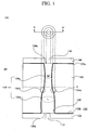
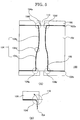
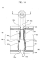
- Fig. 1 (A) is a planar diagram of the through-hole electrode substrate 100 of the present invention related to the present embodiment seen from the upper surface.
- Fig. 1 (B) is a cross-sectional diagram of the line A ⁇ A' in Fig. 1 (A) . Both Fig. 1 (A) and (B) show a part of the through-hole electrode substrate 100 of the present invention related to the present embodiment for the convenience of explanation.
- the through-hole electrode substrate 100 of the present invention related to the present embodiment is arranged with a substrate 102, a through-hole 104, a filler 105, insulation layers 106 and 108, and via's 110 and 112. Furthermore, a wiring structure body and electronic components and the like may also be further mounted respectively on a first surface 102a and second surface 102b side of the substrate 102.
- the substrate 102 includes insulation properties, for example it is possible to use glass, sapphire or resin and the like. Although there is no particular limitation to the thickness of the substrate 102, it is possible to appropriately set the thickness to a range of 10 ⁇ m ⁇ 1mm for example.
- the through-hole 104 is a through-hole which passes through a first aperture 104a arranged in the first surface 102a of the substrate and a second aperture 104b arranged in the second surface 102b which is the opposite side surface to the first surface 102a.
- the shape of the through-hole 104 is not constant and changes from the first aperture 104a towards the second aperture 104b.
- the shape of the side wall of the through-hole 104 is not constant and changes from the first aperture 104a towards the second aperture 104b.
- the second aperture 104b is larger than the first aperture 104a and the through-hole 104 includes a narrow part between the first aperture 104a and second aperture 104b.
- the through-hole 104 includes a minimum aperture part 104c having a minimum area M in a planar view (that is, seen from the upper surface), an inflection point 104d (curved line including the inflection point 104d) at which a side wall of the through-hole 104 changes according to a curved line in a cross-sectional view (that is, seen along the cross-section A ⁇ A'), and a maximum aperture part 104e having a maximum area L in a planar view (that is, seen from the upper surface).
- the inflection point 104d of the through-hole 104 is arranged nearer to the second aperture 104b than the center of the through-hole 104, the present embodiment is not limited to this and the inflection point 104d of the through-hole 104 may also be arranged nearer to the first aperture 104a than the center of the through-hole 104. Furthermore, it is possible to form the through-hole 104 by performing an etching process, laser process and sandblast process of the substrate 102. Although there is no particular limitation to the size of the through-hole 104, it is preferred that the size of the maximum aperture part 104e is set to 200 ⁇ m or less in order to realize a narrow pitch.
- the filler 105 is arranged within the through-hole 104.
- the filler 105 is a material with conductive properties, for example, a metal deposit such as Cu, a conductive paste including Cu, and a conductive material such as a conductive resin can be used.
- An electrolytic plating filler method is used in the case where a metal such as Cu is used as the filler 105.
- a conductive paste having fluidity is used as the filler 105 or a conductive resin is used as the material, it is possible to fill the through-hole 104 with a conductive paste or conductive resin using a spatula or scriber and subsequently form the filler 105 by performing a heating process or the like.
- the insulation layers 106 and 108 are respectively arranged directly or via an intermediate layer (not shown in the diagram) above the first surface 102a and second surface 102b of the substrate 102.
- the insulation layers 106 and 108 are formed from a resin material with insulation properties such as polyimide or benzocyclobutene for example, and may be an insulator having a gas discharge function.
- the insulation layers 106 and 108 work as a gas discharge member by discharging (allowing gas to pass through) gas generated and discharged within the through-hole 104 to the exterior. At least one of the insulation layers (gas discharge member) 106 and 108 is arranged so as to contact the filler 105 exposed to the first surface 102a and second surface 102b of the substrate 102.
- a part of the insulation layers (gas discharge member) 106 and 108 may be arranged between the side wall of the through-hole 104 and the filler 105, that is, the insulation layers 106 and 108 may enter between the side wall of the through-hole 104 and the filler 105.
- the insulation layers 106 and 108 are formed by a desired patterning using photolithography using a photosensitive material with insulation properties for example.
- the through-hole 104 includes a minimum aperture part 104c, inflection point 104d and maximum aperture part 104e.
- the filler 105 is filled into the through-hole 104.
- the area where the gas discharge member 108 of the second surface 102b side contacts the filler 105 increases more than the area where the gas discharge member 106 of the first surface 102a side contacts the filler 105, and the amount of gas discharged from the gas discharge member 108 of the second surface side may be set to increase. Furthermore, since the second aperture 104b is larger than the first aperture 104a, it is possible to easily obtain the contact surface relationship described above by setting the diameter of the via 110 and via 112 roughly the same.
- the via 110 and via 112 which are apertures, are holes formed respectively in the insulation layers (gas discharge members) 106 and 108.
- wiring is formed in the via 110 and 112 by plating or sputtering. This wiring contacts with the filler 105 arranged within the through-hole 104 and the wiring conducts with each other.
- the via 110 and 112 which are apertures in the insulation layers (gas discharge member) 106 and 108 are formed respectively overlapping a first aperture and a second aperture of the substrate 102.
- the via 110 and 112 which are apertures in the insulation layers (gas discharge member) 106 and 108 are respectively arranged directly above the first aperture and second aperture of the substrate 102.
- a part of the via 110 and/or the via 112 which are apertures in the insulation layers (gas discharge member) 106 and 108 may be formed so as to overlap the first aperture 104a and second aperture 104b of the substrate 102 respectively.
- the through-hole 104 includes a minimum aperture part 104c, inflection point 104d and maximum aperture part 104e.
- the filler 105 is filled into the through-hole 104. It is possible to secure filler properties of the filler by making the size of the first aperture 104a and second aperture 104b different. In addition, in the case where a force is applied to the filler 105 in the direction of the first surface 102a, it is possible to prevent the filler 105 from dropping out of the substrate 102 due to the presence of the inflection point 104d.
- the through-hole electrode substrate 100 related to the present embodiment may include both or only one of either the minimum aperture part 104c and maximum aperture part 104e. Therefore, in the through-hole electrode substrate 100 of the present invention related to the present embodiment, it is possible to secure filler properties of the filler 105 and prevent the filler 105 from dropping in either an upwards or downwards direction.
- the insulation layers (gas discharge member) 106 and 108 is arranged so as to contact with the filler 105 exposed to the first surface 102a and second surface 102b of the substrate 102. Therefore, it is possible for the insulation layer (gas discharge member) 106 and/or 108 to discharge gas generated and discharged within the through-hole 104 to the exterior, remove defects caused by accumulated gas in a gas reservoir within the through-hole 104, it is possible to prevent the filler 105 from dropping out from the through-hole 104, and it is possible to provide a through-hole electrode substrate with a high level of reliability.
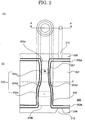
- Fig. 2 (A) is a planar diagram of the through-hole electrode substrate 200 of the present invention related to the present embodiment seen from the upper surface.
- Fig. 2 (B) is a cross-sectional diagram of the line A ⁇ A' in Fig. 2 (A) . Both Fig. 2 (A) and (B) show a part of the through-hole electrode substrate 200 of the present invention related to the present embodiment for the convenience of explanation.
- the through-hole electrode substrate 200 of the present invention related to the present embodiment is arranged with a substrate 202, a through-hole 204, a filler 205, insulation layers 206 and 208, and via's 210 and 212. Furthermore, a wiring structure body and electronic components and the like may also be further mounted respectively on a first surface 202a and second surface 202b side of the substrate 202.
- the substrate 202 includes insulation properties, for example it is possible to use glass, sapphire or resin and the like. Although there is no particular limitation to the thickness of the substrate 202, it is possible to appropriately set the thickness to a range of 10 ⁇ m ⁇ 1mm for example.
- the through-hole 204 is a through-hole which passes through a first aperture 204a arranged in the first surface 202a of the substrate 202 and a second aperture 204b arranged in the second surface 202b which is the opposite side surface to the first surface 202a.
- the shape of the through-hole 204 is not constant and changes from the first aperture 204a towards the second aperture 204b the same as in the first embodiment described above. In other words, the shape of the side wall of the through-hole 204 is not constant and changes from the first aperture 204a towards the second aperture 204b.
- the second aperture 204b is larger than the first aperture 204a and the through-hole 204 includes a narrow part between the first aperture 204a and second aperture 204b.
- the through-hole 204 includes a minimum aperture part 204c having a minimum area M in a planar view (that is, seen from the upper surface), an inflection point 204d (curved line including the inflection point 204d) at which a side wall of the through-hole 204 changes according to a curved line in a cross-sectional view (that is, seen along the cross-section A ⁇ A'), and a maximum aperture part 204e having a maximum area L in a planar view (that is, seen from the upper surface).
- the inflection point 204d of the through-hole 204 is arranged nearer to the second aperture 204b than the center of the through-hole 204, the present embodiment is not limited to this and the inflection point 204d of the through-hole 204 may also be arranged nearer to the first aperture 204a than the center of the through-hole 204. Furthermore, it is possible to form the through-hole 204 by performing an etching process, laser process and sandblast process of the substrate 202. Although there is no particular limitation to the size of the through-hole 204, it is preferred that the size of the maximum aperture part 204e is set to 200 ⁇ m or less in order to realize a narrow pitch.
- a conductive film 207 and the filler 205 are arranged within the through-hole 204.
- the conductive film 207 is arranged on the side wall side of the through-hole 204 and a part of the conductive film 207 is arranged on an upper part of the first surface 202a and second surface 202b.
- the filler 205 is a material with insulation properties, for example, an organic material such as polyimide or benzocyclobutene or an inorganic material such as silicon oxide or silicon nitride is used.
- the conductive film 207 can be formed using a plating method or CVD method for example.
- the filler 205 can be formed using a method such as absorption or pushing method.
- the insulation layers 206 and 208 are respectively arranged directly or via an intermediate layer (not shown in the diagram) above the first surface 202a and second surface 202b of the substrate 202.
- the insulation layers 206 and 208 are formed from a resin material with insulation properties such as polyimide or benzocyclobutene for example, and may be an insulator having a gas discharge function.
- the insulation layers 206 and 208 work as a gas discharge member by discharging (allowing gas to pass through) gas generated and discharged within the through-hole 204 to the exterior.
- the insulation layers (gas discharge member) 206 and 208 are arranged so as to cover and contact the filler 205 which is exposed to the first surface 202a and second surface 202b of the substrate 202.
- At least one of the insulation layers (gas discharge member) 206 and 208 is arranged so as to contact the filler 205 exposed to the first surface 202a and second surface 202b of the substrate 202.
- a part of the insulation layers (gas discharge member) 206 and 208 may be arranged between the side wall of the through-hole 204 and the filler 205, that is, the insulation layers 206 and 208 may enter between the side wall of the through-hole 204 and the filler 205.
- the insulation layers 206 and 208 are formed by a desired patterning using photolithography using a photosensitive material with insulation properties for example.
- the through-hole 204 includes a minimum aperture part 204c, inflection point 204d and maximum aperture part 204e.
- the filler 205 is filled into the through-hole 204. In the case shown in Fig. 2 , there is a larger amount of the filler 205 in the part of the through-hole 204 on the second surface 202b side than the part of the through-hole 204 on the first surface 202a side and due to this the amount of gas which is discharged increases.
- the area where the gas discharge member 208 of the second surface 202b side contacts the filler 205 increases more than the area where the gas discharge member 206 of the first surface 202a side contacts the filler 205, and the amount of gas discharged from the gas discharge member 208 of the second surface side may be set to increase.
- the via 210 and via 212 which are apertures, are holes formed respectively in the insulation layers (gas discharge members) 206 and 208 above the conductive film 207 above the first surface 202a and second surface 202b.
- wiring is formed in the via 210 and 212 by plating or sputtering. This wiring contacts with the conductive film 207 above the first surface 202a and above the second surface 202b and the wiring conducts with each other.
- a part of the via 210 and/or the via 212 which are apertures in the insulation layers (gas discharge member) 206 and 208 may be formed so as to overlap the first aperture 204a and second aperture 204b of the substrate 202 respectively.
- the through-hole 204 includes a minimum aperture part 204c, inflection point 204d and maximum aperture part 204e.
- the filler 205 is filled into the through-hole 204. It is possible to secure filler properties of the filler by making the size of the first aperture 204a and second aperture 204b different. In addition, in the case where a force is applied to the filler 205 in the direction of the first surface 202a, it is possible to prevent the filler 205 from dropping out of the substrate 202 due to the presence of the inflection point 204d.
- the through-hole electrode substrate 200 related to the present embodiment may include both or only one of either the minimum aperture part 204c and maximum aperture part 204e. Therefore, in the through-hole electrode substrate 200 of the present invention related to the present embodiment, it is possible to secure filler properties of the filler 205 and prevent the filler 205 from dropping in either an upwards or downwards direction.
- the insulation layers (gas discharge member) 206 and 208 is arranged so as to contact with the filler 205 exposed to the first surface 202a and second surface 202b of the substrate 202. Therefore, it is possible for the insulation layer (gas discharge member) 206 and/or 208 to discharge gas generated and discharged within the through-hole 204 to the exterior, remove defects caused by accumulated gas in a gas reservoir within the through-hole 204, it is possible to prevent the filler 205 from dropping out from the through-hole 204, and it is possible to provide a through-hole electrode substrate with a high level of reliability.
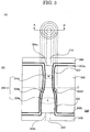
- Fig. 3 (A) is a planar diagram of the through-hole electrode substrate 300 of the present invention related to the present embodiment seen from the upper surface.
- Fig. 3 (B) is a cross-sectional diagram of the line A ⁇ A' in Fig. 3 (A) . Both Fig. 3 (A) and (B) show a part of the through-hole electrode substrate 300 of the present invention related to the present embodiment for the convenience of explanation.
- the through-hole electrode substrate 300 of the present invention related to the present embodiment is arranged with a substrate 302, a through-hole 304, a filler 305, insulation layers 306 and 308, and via's 310 and 312. Furthermore, a wiring structure body and electronic components and the like may also be further mounted respectively on a first surface 302a and second surface 302b side of the substrate 302.
- the substrate 302 includes conductive properties, for example it is possible to use a silicon semiconductor or metal such as stainless steel and the like. Although there is no particular limitation to the thickness of the substrate 302, it is possible to appropriately set the thickness to a range of 10 ⁇ m ⁇ 1mm for example.
- the through-hole 304 is a through-hole which passes through a first aperture 304a arranged in the first surface 302a of the substrate 302 and a second aperture 304b arranged in the second surface 302b which is the opposite side surface to the first surface 302a the same as in the first and second embodiments described above.
- the shape of the through-hole 304 is not constant and changes from the first aperture 304a towards the second aperture 304b.
- the shape of the side wall of the through-hole 304 is not constant and changes from the first aperture 304a towards the second aperture 304b.
- the second aperture 304b is larger than the first aperture 304a and the through-hole 304 includes a narrow part between the first aperture 304a and second aperture 304b.
- the through-hole 304 includes a minimum aperture part 304c having a minimum area M in a planar view (that is, seen from the upper surface), an inflection point 304d (curved line including the inflection point 304d) at which a side wall of the through-hole 304 changes according to a curved line in a cross-sectional view (that is, seen along the cross-section A ⁇ A'), and a maximum aperture part 304e having a maximum area L in a planar view (that is, seen from the upper surface).
- the inflection point 304d of the through-hole 304 is arranged nearer to the second aperture 304b than the center of the through-hole 304
- the present embodiment is not limited to this and the inflection point 304d of the through-hole 304 may also be arranged nearer to the first aperture 304a than the center of the through-hole 304.
- the size of the through-hole 304 it is preferred that the size of the maximum aperture part 304e is set to 200 ⁇ m or less in order to realize a narrow pitch.
- the insulation layer 307 and the filler 305 are arranged within the through-hole 304.
- the insulation layer 307 is arranged on the side wall side of the through-hole 304 and a part of the insulation layer 307 is arranged on an upper part of the first surface and second surface of the substrate 302.
- the filler 305 is a material with conductive properties, for example, a metal deposit such as Cu, a conductive paste including Cu, and a conductive material such as a conductive resin can be used.
- An electrolytic plating filler method is used in the case where a metal such as Cu is used as the filler 305.
- a conductive paste having fluidity is used as the filler 305 or a conductive resin is used as the material, it is possible to fill the through-hole 304 with a conductive paste or conductive resin using a spatula or scriber and subsequently form the filler 305 by performing a heating process or the like.
- the insulation layers 306 and 308 are respectively arranged directly or via an intermediate layer (not shown in the diagram) above the first surface 302a and second surface 302b of the substrate 302.
- the insulation layers 306 and 308 are formed from a resin material with insulation properties such as polyimide or benzocyclobutene for example, and may be an insulator having a gas discharge function.
- the insulation layers 306 and 308 work as a gas discharge member by discharging (allowing gas to pass through) gas generated and discharged within the through-hole 304 to the exterior. At least one of the insulation layers (gas discharge member) 306 and 308 is arranged so as to contact the filler 305 exposed to the first surface and second surface of the substrate 302.
- a part of the insulation layers (gas discharge member) 306 and 308 may be arranged between the side wall of the through-hole 304 and the filler 305, that is, the insulation layers 306 and 308 may enter between the side wall of the through-hole 304 and the filler 305.
- the insulation layers 306 and 308 are formed by a desired patterning using photolithography using a photosensitive material with insulation properties for example.
- the through-hole 304 includes a minimum aperture part 304c, inflection point 304d and maximum aperture part 304e.
- the filler 305 is filled into the through-hole 304.
- the area where the gas discharge member 308 of the second surface side contacts the filler 305 increases more than the area where the gas discharge member 306 of the first surface 302a side contacts the filler 305, and the amount of gas discharged from the gas discharge member 308 of the second surface 302b side may be set to increase. Furthermore, since the second aperture 304b is larger than the first aperture 304a, it is possible to easily obtain the contact surface relationship described above by setting the diameter of the via 310 and via 312 roughly the same.
- the via 310 and via 312 which are apertures, are holes formed respectively in the insulation layers (gas discharge members) 306 and 308.
- wiring is formed in the via 310 and 312 by plating or sputtering. This wiring contacts with the filler 305 arranged within the through-hole 304 and the wiring conducts with each other.
- the via 310 and 312 which are apertures in the insulation layers (gas discharge member) 306 and 308 are formed respectively overlapping the first aperture 304a and the second aperture 304b of the substrate 302.
- the via 310 and 312 which are apertures in the insulation layers (gas discharge member) 306 and 308 are respectively arranged directly above the first aperture 304a and second aperture 304b of the substrate 302.
- a part of the via 310 and/or the via 312 which are apertures in the insulation layers (gas discharge member) 306 and 308 may be formed so as to overlap the first aperture 304a and second aperture 304b of the substrate 302 respectively.
- the through-hole 304 includes a minimum aperture part 304c, inflection point 304d and maximum aperture part 304e.
- the filler 305 is filled into the through-hole 304. It is possible to secure filler properties of the filler by making the size of the first aperture 304a and second aperture 304b different. In addition, in the case where a force is applied to the filler 305 in the direction of the first surface 302a, it is possible to prevent the filler 305 from dropping out of the substrate 302 due to the presence of the inflection point 304d.
- the through-hole electrode substrate 300 related to the present embodiment may include both or only one of either the minimum aperture part 304c and maximum aperture part 304e. Therefore, in the through-hole electrode substrate 300 of the present invention related to the present embodiment, it is possible to secure filler properties of the filler 305 and prevent the filler 305 from dropping in either an upwards or downwards direction.
- the insulation layers (gas discharge member) 306 and 308 is arranged so as to contact with the filler 305 exposed to the first surface 302a and second surface 302b of the substrate 302. Therefore, it is possible for the insulation layer (gas discharge member) 306 and/or 308 to discharge gas generated and discharged within the through-hole 304 to the exterior, remove defects caused by accumulated gas in a gas reservoir within the through-hole 304, it is possible to prevent the filler 305 from dropping out from the through-hole 304, and it is possible to provide a through-hole electrode substrate with a high level of reliability.
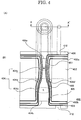
- Fig. 4 (A) is a planar diagram of the through-hole electrode substrate 400 of the present invention related to the present embodiment seen from the upper surface.
- Fig. 4 (B) is a cross-sectional diagram of the line A ⁇ A' in Fig. 4 (A) . Both Fig. 4 (A) and (B) show a part of the through-hole electrode substrate 400 of the present invention related to the present embodiment for the convenience of explanation.
- the through-hole electrode substrate 400 of the present invention related to the present embodiment is arranged with a substrate 402, a through-hole 404, a filler 405, insulation layers 406 and 408, insulation film 407, a conductive film 409, and via's 410 and 412. Furthermore, a wiring structure body and electronic components and the like may also be further mounted respectively on a first surface 402a and second surface 402b side of the substrate 402.
- the substrate 402 includes conductive properties, for example it is possible to use a silicon semiconductor or metal such as stainless steel and the like. Although there is no particular limitation to the thickness of the substrate 402, it is possible to appropriately set the thickness to a range of 10 ⁇ m ⁇ 1mm for example.
- the through-hole 404 is a through-hole which passes through a first aperture 404a arranged in the first surface 402a of the substrate 402 and a second aperture 404b arranged in the second surface 402b which is the opposite side surface to the first surface 402a.
- the shape of the through-hole 404 is not constant and changes from the first aperture 404a towards the second aperture 404b the same as the first to third embodiments described above. In other words, the shape of the side wall of the through-hole 404 is not constant and changes from the first aperture 404a towards the second aperture 404b.
- the second aperture 404b is larger than the first aperture 404a and the through-hole 404 includes a narrow part between the first aperture 404a and second aperture 404b.
- the through-hole 404 includes a minimum aperture part 404c having a minimum area M in a planar view (that is, seen from the upper surface), an inflection point 404d (curved line including the inflection point 404d) at which a side wall of the through-hole 404 changes according to a curved line in a cross-sectional view (that is, seen along the cross-section A ⁇ A'), and a maximum aperture part 404e having a maximum area L in a planar view (that is, seen from the upper surface).
- the inflection point 404d of the through-hole 404 is arranged nearer to the second aperture 404b than the center of the through-hole 404, the present embodiment is not limited to this and the inflection point 404d of the through-hole 404 may also be arranged nearer to the first aperture 404a than the center of the through-hole 404. Furthermore, it is possible to form the through-hole 404 by performing an etching process, laser process and sandblast process of the substrate 402. Although there is no particular limitation to the size of the through-hole 404, it is preferred that the size of the maximum aperture part 404e is set to 200 ⁇ m or less in order to realize a narrow pitch.
- the insulation layer 407, conductive film 409 and the filler 405 are arranged within the through-hole 404.
- the insulation layer 407 is arranged on the side wall side of the through-hole 404, and a part of the insulation layer 407 is arranged on an upper part of the first surface and second surface of the substrate 402.
- the conductive film 409 is arranged on the insulation layer 407 side of the through-hole 404 and a part of the conductive film 409 is arranged on an upper part of the first surface and second surface of the substrate 402.
- the filler 405 is a material with insulation properties, for example, an organic material such as polyimide or benzocyclobutene or an inorganic material such as silicon oxide or silicon nitride is used.
- the conductive film 409 can be formed using a plating method or CVD method for example.
- the filler 405 can be formed using a method such as absorption or pushing method.
- the insulation layers 406 and 408 are respectively arranged directly or via an intermediate layer (not shown in the diagram) above the first surface 402a and second surface 402b of the substrate 402.
- the insulation layers 406 and 408 are formed from a resin material with insulation properties such as polyimide and may be an insulator having a gas discharge function.
- the insulation layers 406 and 408 work as a gas discharge member by discharging (allowing gas to pass through) gas generated and discharged within the through-hole 404 to the exterior.
- the insulation layers (gas discharge member) 406 and 408 are arranged to cover and contact the filler 405 exposed to the first surface and second surface of the substrate 402.
- At least one of the insulation layers (gas discharge member) 406 and 408 is arranged so as to contact the filler 405 exposed to the first surface 402a and second surface 402b of the substrate 402.
- a part of the insulation layers (gas discharge member) 406 and 408 may be arranged between the side wall of the through-hole 404 and/or the insulation layer 407 and the filler 405, that is, the insulation layers 406 and 408 may enter between the side wall of the through-hole 404 and the filler 405.
- the insulation layers 406 and 408 are formed by a desired patterning using photolithography using a photosensitive material with insulation properties for example.
- the through-hole 404 includes a minimum aperture part 404c, inflection point 404d and maximum aperture part 404e.
- the filler 405 is filled into the through-hole 404. In the case shown in Fig. 4 , there is a larger amount of the filler 405 in the part of the through-hole 404 on the second surface 402b side than the part of the through-hole 404 on the first surface 402a side and due to this the amount of gas which is discharged increases.
- the area where the gas discharge member 408 of the second surface 402b side contacts the filler 405 increases more than the area where the gas discharge member 406 of the first surface 402a side contacts the filler 405, and the amount of gas discharged from the gas discharge member 408 of the second surface side may be set to increase. Furthermore, since the second aperture 404b is larger than the first aperture 404a, it is possible to easily obtain the contact surface relationship described above by setting the diameter of the via 410 and via 412 roughly the same.
- the via 410 and via 412 which are apertures, are holes formed respectively in the insulation layers (gas discharge members) 406 and 408 above the conductive film 409 above the first surface and second surface.
- wiring is formed in the via 410 and 412 by plating or sputtering. This wiring contacts with the conductive film 409 above the first surface 402a and above the second surface 402b and the wiring conducts with each other.
- a part of the via 410 and/or the via 412 which are apertures in the insulation layers (gas discharge member) 406 and 408 may be formed so as to overlap the first aperture 404a and second aperture 404b of the substrate 402 respectively.
- the through-hole 404 includes a minimum aperture part 404c, inflection point 404d and maximum aperture part 404e.
- the filler 405 is filled into the through-hole 404. It is possible to secure filler properties of the filler by making the size of the first aperture 404a and second aperture 404b different. In addition, in the case where a force is applied to the filler 405 in the direction of the first surface 402a, it is possible to prevent the filler 405 from dropping out of the substrate 402 due to the presence of the inflection point 404d.
- the through-hole electrode substrate 400 related to the present embodiment may include both or only one of either the minimum aperture part 404c and maximum aperture part 404e. Therefore, in the through-hole electrode substrate 400 of the present invention related to the present embodiment, it is possible to secure filler properties of the filler 405 and prevent the filler 405 from dropping in either an upwards or downwards direction.
- the insulation layers (gas discharge member) 406 and 408 is arranged so as to contact with the filler 405 exposed to the first surface 402a and second surface 402b of the substrate 402. Therefore, it is possible for the insulation layer (gas discharge member) 406 and/or 408 to discharge gas generated and discharged within the through-hole 404 to the exterior, remove defects caused by accumulated gas in a gas reservoir within the through-hole 404, it is possible to prevent the filler 405 from dropping out from the through-hole 404, and it is possible to provide a through-hole electrode substrate with a high level of reliability.
- Fig. 5 (A) is a cross-sectional diagram of the through-hole electrode substrate 100 of the present invention related to the present embodiment.
- Fig. 5 (B) is an expanded view diagram of the part 104f in Fig. 5 (A) .
- both Fig. 5 (A) and (B) show a part of the through-hole electrode substrate 100 of the present invention related to the present embodiment for the convenience of explanation.
- the through-hole electrode substrate 100 of the present invention related to the present embodiment includes a connection part 104f with a first surface of the first aperture 101a of the through-hole 104 and the connection part 104f has a curved surface.
- a connection part 104g with a first surface of the first aperture 101a of the through-hole 104 has a curved surface. Since the remaining structure is the same as in the first embodiment, an explanation is omitted.
- connection part 104f and connection part 104g of the through-hole 104 in the through-hole electrode substrate 100 of the present invention related to the present embodiment include a curved surface, it is possible to easily fill the filler 405.
- connection part with a first surface of a first aperture of a through-hole with a curved surface and by providing a connection part of a second surface of a second aperture of a through-hole with a curved surface, it is possible to adopt the same structure as the present embodiment in the first to fourth embodiments described above.
- Fig. 6 (A) is a planar diagram of the through-hole electrode substrate 100 of the present invention related to the present embodiment seen from the upper surface.
- Fig. 6 (B) is a cross-sectional diagram of the line A ⁇ A' in Fig. 6 (A) . Both Fig. 6 (A) and (B) show a part of the through-hole electrode substrate 100 of the present invention related to the present embodiment for the convenience of explanation.
- the through-hole electrode substrate 100 of the present invention related to the present embodiment is arranged with the inflection point 104d of the through hole 104 nearer to the first aperture 104a than the center of the through-hole 104. Since the remaining structure is the same as in the first embodiment, an explanation is omitted.
- Fig. 7 (A) is a planar diagram of the through-hole electrode substrate 100 of the present invention related to the present embodiment seen from the upper surface.
- Fig. 7 (B) is a cross-sectional diagram of the line A ⁇ A' in Fig. 7 (A) . Both Fig. 7 (A) and (B) show a part of the through-hole electrode substrate 100 of the present invention related to the present embodiment for the convenience of explanation.
- the apertures (via's) 110 and 112 of the gas discharge member 106 and 108 are arranged so that the area seen from a planar view (that is, see from an upper surface) becomes larger as they separate from the substrate 102 side.
- an angle ⁇ formed between the gas discharge member 106 and 108 and the filler 105 is about 45 degrees ⁇ 89 degrees. Since the remaining structure is the same as in the first embodiment, an explanation is omitted.
- the insulation layers 106 and 108 are formed by a desired patterning using photolithography using a photosensitive material with insulation properties for example, the apertures (via's) 110 and 112 of the gas discharge members 106 and 108 can be formed so that the area seen from a planar view becomes larger as they separate from the substrate 102 side by adjusting the exposure conditions.
- FIG. 8 (A) and (B) a roughly planar view of the through-hole electrode substrate 100 of the present invention related to the present embodiment is shown in Fig. 8 (A) and (B) .
- the apertures (via's) 110 and 112 of the gas discharge member 106 and 108 are arranged so that the area seen from a planar view (that is, see from an upper surface) becomes larger as they separate from the substrate 102 side, and since it is possible to reduce the area of the apertures (via's) 110 and 112 above the filler 105 and secure a contact between the apertures (via's) 110 and 112 and the filler 105, it is possible to reduce the possibility of contact defects due to misalignment when forming the apertures (via's) 110 and 112.
- Fig. 8 (A) shows the case where the aperture (via) 110 above the filler 105 is misaligned on the right side.
- Fig. 8 (B) shows the case where the aperture (via) 110 above the filler 105 is misaligned on the right side and a part of the aperture (via) 110 becomes separated from above the filler 105.
- Fig. 8 (A) and (B) since it is possible to secure a contact between the apertures (via') 110 and 112 and the filler 105, it is possible to reduce the possibility of contact defects due to misalignment of the apertures (via's) 110 and 112.
- the apertures (via's) 210 and 212 of the gas discharge members 206 and 208 are arranged so that the area seen from a planar view (that is, see from an upper surface) becomes larger as they separate from the substrate 202 side.
- an angle ⁇ formed between the gas discharge members 206 and 208 and the filler 205 is about 45 degrees ⁇ 89 degrees. Since the remaining structure is the same as in the second embodiment, an explanation is omitted.
- the apertures (via's) 310 and 312 of the gas discharge members 306 and 308 are arranged so that the area seen from a planar view (that is, see from an upper surface) becomes larger as they separate from the substrate 302 side.
- an angle ⁇ formed between the gas discharge members 306 and 308 and the filler 305 is about 45 degrees ⁇ 89 degrees. Since the remaining structure is the same as in the third embodiment, an explanation is omitted.
- the apertures (via's) 410 and 412 of the gas discharge members 406 and 408 are arranged so that the area seen from a planar view (that is, see from an upper surface) becomes larger as they separate from the substrate 402 side.
- an angle ⁇ formed between the gas discharge members 406 and 408 and the filler 405 is about 45 degrees ⁇ 89 degrees. Since the remaining structure is the same as in the fourth embodiment, an explanation is omitted.
- a semiconductor device 1000 of the present invention related to the eighth embodiment is explained while referring to Fig. 12 ⁇ 14 .
- a semiconductor device 1000 using the through-hole electrode substrates in the first to seventh embodiments described above is explained.
- Fig. 12 shows a semiconductor device 1000 related to the present embodiment.
- the semiconductor device 1000 is stacked with three through-hole electrode substrates 100 related to the present invention and is connected to a LSI substrate (semiconductor substrate) 500.
- the LSI substrate 500 is arranged with a wiring layer 502.
- Semiconductor elements such as a DRAM for example are arranged above the through-hole electrode substrate 100.
- a wiring layer 120 is arranged in the through-hole electrode substrate 100.
- the wiring layer 502 of the LSI substrate 500 and the wiring layer 120 of the through-hole electrode substrate 100 are connected via a bump 1002.
- a metal such as indium, copper or gold for example is used for the bump 1002.
- the wiring layer 120 of the through-hole electrode substrate 100 is connected with the wiring layer 120 of a different through-hole electrode substrate 100 via the bump 1002.
- the present invention is not limited to three layers in the case where the through-hole electrode substrates 100 are stacked, two layers or four layers are also possible.
- the present invention is not limited to using a bump in the connection between the through-hole electrode substrate 100 and another substrate, eutectic bonding or another bonding technology may also be used.
- the through-hole electrode substrate 100 and another substrate may be adhered together by coating polyimide or an epoxy resin and sintering.
- Fig. 13 shows another example of the semiconductor device 1000 of the present invention related to present embodiment.
- the semiconductor device 1000 shown in Fig. 13 is stacked with a semiconductor chip (LSI chip) 600 and 602 such as a MEMS device, CPU, memory or IC, and the through-hole electrode substrate 100, and is connected to a LSI substrate 500
- the through-hole electrode substrate 100 is arranged between the semiconductor chip 600 and the semiconductor chip 602 and both are connected via a bump 1002.
- the semiconductor chip 600 is mounted above the LSI substrate 500 and the LSI substrate 500 and the semiconductor chip 602 are connected via a wire 604.
- the through-hole electrode substrate 100 is used as an interposer for three-dimensional mounting by stacking a plurality of semiconductor chips, and by stacking a plurality of semiconductor chips each with a different function it is possible to form a multi-functional semiconductor device.
- the semiconductor chip 600 into a tri-axial acceleration sensor and the semiconductor chip 602 into a bi-axial magnetic sensor, it is possible to realize a semiconductor device in which a five-axis motion sensor is realized using one module.
- a semiconductor chip is a sensor formed using a MEMS device
- the sensing results are sometimes output using an analog signal.
- a low pass filter or amplifier and the like may be formed in the semiconductor chip 600, 602 or through-hole electrode substrate 100.
- Fig. 14 shows another example of the semiconductor device 1000 related to the present embodiment.
- the two examples ( Fig. 12 , Fig. 13 ) described above were three-dimensional mounting
- the present example applies the through-hole electrode substrate 100 to a two dimensional and three dimensional combined mounting.
- six through-hole electrode substrates 100 are stacked and connected to the LSI substrate 500.
- the through-hole electrode substrates 100 are stacked but are also arranged aligned in a substrate in-plane direction.
- two through-hole electrode substrates 100 are connected above the LSI substrate 500, a further through-hole electrode substrate 100 is arranged above the two through-hole electrode substrates 100, and a further through-hole electrode substrate 100 is arranged above.
- two dimensional and three dimensional combined mounting is possible even when the through-hole electrode substrate 100 is used as an interposer or connecting a plurality of semiconductor chips.
- several through-hole electrode substrates 100 may be replaced for a semiconductor chip.
- the present invention is not limited to this and the through-hole electrode substrates 200, 300 and/or 400 of the present invention related to the other embodiments may also be used.
- the semiconductor device 1000 of the present invention related to the present embodiment is mounted in various electronic devices for example in a mobile terminal (mobile phone, smartphone and note type personal computer and the like), a data processing device (desktop type personal computer, server, car navigation and the like) and household appliances and the like.
- a mobile terminal mobile phone, smartphone and note type personal computer and the like
- a data processing device desktop type personal computer, server, car navigation and the like
- household appliances and the like for example in a mobile terminal (mobile phone, smartphone and note type personal computer and the like), a data processing device (desktop type personal computer, server, car navigation and the like) and household appliances and the like.
Landscapes
- Engineering & Computer Science (AREA)
- Microelectronics & Electronic Packaging (AREA)
- Power Engineering (AREA)
- Physics & Mathematics (AREA)
- Condensed Matter Physics & Semiconductors (AREA)
- General Physics & Mathematics (AREA)
- Computer Hardware Design (AREA)
- Manufacturing & Machinery (AREA)
- Printing Elements For Providing Electric Connections Between Printed Circuits (AREA)
- Internal Circuitry In Semiconductor Integrated Circuit Devices (AREA)
- Photovoltaic Devices (AREA)
Description
- The present invention is related to a through-hole electrode substrate arranged with a through-hole electrode which passes through a top surface and rear surface of a substrate. In particular, the present invention is related to a through-hole electrode substrate used as an interposer substrate for connecting a plurality of elements. In addition, the present invention is related to a semiconductor device which uses the through-hole electrode substrate.
- In recent years, the development of through-hole electrode substrates arranged with a conductive part which conducts a top surface and rear surface of a substrate as an interposer between LSI chips is progressing. This type of through-hole electrode substrate is formed with a through-hole electrode by filling a conductive material using electrolytic plating and the like within a through-hole.
- A LSI chip which has a narrow pitch and wiring with short dimensions is arranged on an upper surface of a through-hole electrode substrate. In addition, a semiconductor mounted substrate which has a wide pitch and wiring with long dimensions is arranged on the rear surface of a through-hole electrode substrate. The following documents are conventional technologies of a through-hole electrode substrate.
-
- Patent Document 1: Japanese Laid Open Patent No.
2005-514386 - Patent Document 2: Japanese Laid Open Patent No.
2010-548587 - Patent Document 3: Japanese Laid Open Patent No.
2003-513037 - Patent Document 4: Japanese Laid Open Patent No.
2011-528851 - Patent Document 5:
PCT Publication 2010/087483 - Patent Document 6:
PCT Publication 2005/034594 - Patent Document 7:
PCT Publication 2003/007370 - Patent Document 7:
PCT Publication 2011/024921 - Patent Document 8: Japanese Patent No.
4241202 - Patent Document 9: Japanese Patent No.
4203277 - Patent Document 10: Japanese Patent No.
4319831 - Patent Document 11: Japanese Patent No.
4022180 - Patent Document 12: Japanese Patent No.
4564342 - Patent Document 13: Japanese Patent No.
4835141 - Patent Document 14: Japanese Patent No.
5119623 - Patent Document 15: Japanese Laid Open Patent No.
2009-23341 - Patent Document 16: Japanese Patent No.
2976955 - Patent Document 17: Japanese Laid Open Patent No.
2003-243396 - Patent Document 18: Japanese Laid Open Patent No.
2003-198069 - Patent Document 19: Japanese Patent No.
4012375 - Patent Document 20:
US2003/137056 US-Patent Application Publication - In the through-hole electrode, a conductive material is filled into a through-hole as a filler as described above, or a conductive film is formed along the side wall of the through-hole and an insulating resin is filled to the remainder of the through-hole. In the through-hole electrode, a technique is known in which the interior of the through-hole is provided with a taper or a plurality of crater shaped irregularities is formed inside the through- hole in order to prevent dropout of a filler filled in the through-hole (Patent Document 3, Patent Document 4).
- However, even when attempting to prevent dropout of the filler by such a technique, a gap is generated between the filler and the side wall of the through-hole and a gas reservoir may be generated. When heat is applied to the substrate in this state, in the prior art there is a possibility that gas which has collected into a gas reservoir expands causing destruction of the through-hole or filler which causes defects such as dropout of the filler.
- Therefore, the present invention has been made in view of such problems and provides a through-hole electrode substrate and semiconductor device which can eliminate defects due to gas collecting in a gas reservoir in a through-hole and allows prevention of dropout of a filler from within the through-hole.
- According to the present invention, a through-hole electrode substrate according to
claim 1 is provided. Advantageous additional aspects are specified in the dependent claims. - According to the present invention, it is possible to provide a through-hole electrode substrate and a semiconductor device with a high level of reliability which can eliminate defects due to gas collecting in a gas reservoir in a through-hole and allows prevention of dropout of a filler from within the through-hole.
-
-
Fig. 1 is a diagram showing a structure of a through-hole electrode substrate 100 of the present invention related to a first embodiment; -
Fig. 2 is a diagram showing a structure of a through-hole electrode substrate 200 of the present invention related to a second embodiment; -
Fig. 3 is a diagram showing a structure of a through-hole electrode substrate 300 of the present invention related to a third embodiment; -
Fig. 4 is a diagram showing a structure of a through-hole electrode substrate 400 of the present invention related to a fourth embodiment; -
Fig. 5 is a diagram showing a structure of the through-hole electrode substrate 100 of the present invention related to a fifth embodiment; -
Fig. 6 is a diagram showing a structure of the through-hole electrode substrate 100 of the present invention related to a sixth embodiment; -
Fig. 7 is a diagram showing a structure of the through-hole electrode substrate 100 of the present invention related to a seventh embodiment; -
Fig. 8 shows an example in which an aperture (via) 110 of afiller 105 is misaligned in the through-hole electrode substrate 100 of the present invention related to the seventh embodiment; -
Fig. 9 is a diagram showing a structure of the through-hole electrode substrate 300 of the present invention related to the seventh embodiment; -
Fig. 10 is a diagram showing a structure of the through-hole electrode substrate 300 of the present invention related to the seventh embodiment; -
Fig. 11 is a diagram showing a structure of the through-hole electrode substrate 400 of the present invention related to the seventh embodiment; -
Fig. 12 is a diagram showing a structure of a through-hole electrode substrate 1000 of the present invention related to an eighth embodiment; -
Fig. 13 is a diagram showing a structure of the through-hole electrode substrate 1000 of the present invention related to the eighth embodiment; and -
Fig. 14 is a diagram showing a structure of the through-hole electrode substrate 1000 of the present invention related to the eighth embodiment. - A through-hole electrode substrate of the present invention is explained in detail below while referring to the diagrams. The through-hole electrode substrate of the present invention is not limited to the embodiments below and various modifications are possible. In all of the embodiments, the same symbols are attached to the same structural elements and explained.
- The structure of a through-
hole electrode substrate 100 of the present invention related to the present embodiment is explained while referring toFig. 1. Fig. 1 (A) is a planar diagram of the through-hole electrode substrate 100 of the present invention related to the present embodiment seen from the upper surface.Fig. 1 (B) is a cross-sectional diagram of the line A ∼ A' inFig. 1 (A) . BothFig. 1 (A) and (B) show a part of the through-hole electrode substrate 100 of the present invention related to the present embodiment for the convenience of explanation. - The through-
hole electrode substrate 100 of the present invention related to the present embodiment is arranged with asubstrate 102, a through-hole 104, afiller 105, insulation layers 106 and 108, and via's 110 and 112. Furthermore, a wiring structure body and electronic components and the like may also be further mounted respectively on afirst surface 102a andsecond surface 102b side of thesubstrate 102. - In the present embodiment, the
substrate 102 includes insulation properties, for example it is possible to use glass, sapphire or resin and the like. Although there is no particular limitation to the thickness of thesubstrate 102, it is possible to appropriately set the thickness to a range of 10µm ∼ 1mm for example. - The through-
hole 104 is a through-hole which passes through afirst aperture 104a arranged in thefirst surface 102a of the substrate and asecond aperture 104b arranged in thesecond surface 102b which is the opposite side surface to thefirst surface 102a. The shape of the through-hole 104 is not constant and changes from thefirst aperture 104a towards thesecond aperture 104b. In other words, the shape of the side wall of the through-hole 104 is not constant and changes from thefirst aperture 104a towards thesecond aperture 104b. Typically, thesecond aperture 104b is larger than thefirst aperture 104a and the through-hole 104 includes a narrow part between thefirst aperture 104a andsecond aperture 104b. More specifically, the through-hole 104 includes aminimum aperture part 104c having a minimum area M in a planar view (that is, seen from the upper surface), aninflection point 104d (curved line including theinflection point 104d) at which a side wall of the through-hole 104 changes according to a curved line in a cross-sectional view (that is, seen along the cross-section A ∼ A'), and amaximum aperture part 104e having a maximum area L in a planar view (that is, seen from the upper surface). In the present embodiment, although theinflection point 104d of the through-hole 104 is arranged nearer to thesecond aperture 104b than the center of the through-hole 104, the present embodiment is not limited to this and theinflection point 104d of the through-hole 104 may also be arranged nearer to thefirst aperture 104a than the center of the through-hole 104. Furthermore, it is possible to form the through-hole 104 by performing an etching process, laser process and sandblast process of thesubstrate 102. Although there is no particular limitation to the size of the through-hole 104, it is preferred that the size of themaximum aperture part 104e is set to 200µm or less in order to realize a narrow pitch. - The
filler 105 is arranged within the through-hole 104. In the present embodiment, thefiller 105 is a material with conductive properties, for example, a metal deposit such as Cu, a conductive paste including Cu, and a conductive material such as a conductive resin can be used. An electrolytic plating filler method is used in the case where a metal such as Cu is used as thefiller 105. In the case where a conductive paste having fluidity is used as thefiller 105 or a conductive resin is used as the material, it is possible to fill the through-hole 104 with a conductive paste or conductive resin using a spatula or scriber and subsequently form thefiller 105 by performing a heating process or the like. - The insulation layers 106 and 108 are respectively arranged directly or via an intermediate layer (not shown in the diagram) above the
first surface 102a andsecond surface 102b of thesubstrate 102. The insulation layers 106 and 108 are formed from a resin material with insulation properties such as polyimide or benzocyclobutene for example, and may be an insulator having a gas discharge function. The insulation layers 106 and 108 work as a gas discharge member by discharging (allowing gas to pass through) gas generated and discharged within the through-hole 104 to the exterior. At least one of the insulation layers (gas discharge member) 106 and 108 is arranged so as to contact thefiller 105 exposed to thefirst surface 102a andsecond surface 102b of thesubstrate 102. In addition, in the case where a gap exists between the side wall of the through-hole 104 and thefiller 105, a part of the insulation layers (gas discharge member) 106 and 108 may be arranged between the side wall of the through-hole 104 and thefiller 105, that is, the insulation layers 106 and 108 may enter between the side wall of the through-hole 104 and thefiller 105. The insulation layers 106 and 108 are formed by a desired patterning using photolithography using a photosensitive material with insulation properties for example. - In the through-
hole electrode substrate 100 of the present invention related to the present embodiment, as described above, the through-hole 104 includes aminimum aperture part 104c,inflection point 104d andmaximum aperture part 104e. In addition, thefiller 105 is filled into the through-hole 104. In the case shown inFig. 1 , there is a larger amount of thefiller 105 in the part of the through-hole 104 on thesecond surface 102b side than the part of the through-hole 104 on thefirst surface 102a side and due to this the amount of gas which is discharged increases. The area where thegas discharge member 108 of thesecond surface 102b side contacts thefiller 105 increases more than the area where thegas discharge member 106 of thefirst surface 102a side contacts thefiller 105, and the amount of gas discharged from thegas discharge member 108 of the second surface side may be set to increase. Furthermore, since thesecond aperture 104b is larger than thefirst aperture 104a, it is possible to easily obtain the contact surface relationship described above by setting the diameter of the via 110 and via 112 roughly the same. - The via 110 and via 112 which are apertures, are holes formed respectively in the insulation layers (gas discharge members) 106 and 108. Although not shown in the diagram for the convenience of explanation, wiring is formed in the via 110 and 112 by plating or sputtering. This wiring contacts with the
filler 105 arranged within the through-hole 104 and the wiring conducts with each other. As is shown inFig. 1 (B) , the via 110 and 112 which are apertures in the insulation layers (gas discharge member) 106 and 108 are formed respectively overlapping a first aperture and a second aperture of thesubstrate 102. In other words, the via 110 and 112 which are apertures in the insulation layers (gas discharge member) 106 and 108 are respectively arranged directly above the first aperture and second aperture of thesubstrate 102. In addition, a part of the via 110 and/or the via 112 which are apertures in the insulation layers (gas discharge member) 106 and 108 may be formed so as to overlap thefirst aperture 104a andsecond aperture 104b of thesubstrate 102 respectively. - In the through-
hole electrode substrate 100 of the present invention related to the present embodiment, as described above, the through-hole 104 includes aminimum aperture part 104c,inflection point 104d andmaximum aperture part 104e. In addition, thefiller 105 is filled into the through-hole 104. It is possible to secure filler properties of the filler by making the size of thefirst aperture 104a andsecond aperture 104b different. In addition, in the case where a force is applied to thefiller 105 in the direction of thefirst surface 102a, it is possible to prevent thefiller 105 from dropping out of thesubstrate 102 due to the presence of theinflection point 104d. In addition, in the case where a force is applied to thefiller 105 in the direction of thesecond surface 102b, it is possible to prevent thefiller 105 from dropping out of thesubstrate 102 due to the presence of theminimum aperture part 104c. Furthermore, the through-hole electrode substrate 100 related to the present embodiment may include both or only one of either theminimum aperture part 104c andmaximum aperture part 104e. Therefore, in the through-hole electrode substrate 100 of the present invention related to the present embodiment, it is possible to secure filler properties of thefiller 105 and prevent thefiller 105 from dropping in either an upwards or downwards direction. - In addition, in the through-
hole electrode substrate 100 of the present invention related to the present embodiment, as described above, at least one of the insulation layers (gas discharge member) 106 and 108 is arranged so as to contact with thefiller 105 exposed to thefirst surface 102a andsecond surface 102b of thesubstrate 102. Therefore, it is possible for the insulation layer (gas discharge member) 106 and/or 108 to discharge gas generated and discharged within the through-hole 104 to the exterior, remove defects caused by accumulated gas in a gas reservoir within the through-hole 104, it is possible to prevent thefiller 105 from dropping out from the through-hole 104, and it is possible to provide a through-hole electrode substrate with a high level of reliability. - Furthermore, although it preferred that there is no gap between the side wall of the through-
hole 104 and thefiller 105, a slight gap or interval may be produced between the side wall of the through-hole 104 and thefiller 105. Even in the case where this type of gap or interval is produced, it is possible to prevent thefiller 105 from dropping out in the through-hole electrode substrate 100 of the present invention related to the present embodiment. - The structure of a through-
hole electrode substrate 200 of the present invention related to the present embodiment is explained while referring toFig. 2. Fig. 2 (A) is a planar diagram of the through-hole electrode substrate 200 of the present invention related to the present embodiment seen from the upper surface.Fig. 2 (B) is a cross-sectional diagram of the line A ∼ A' inFig. 2 (A) . BothFig. 2 (A) and (B) show a part of the through-hole electrode substrate 200 of the present invention related to the present embodiment for the convenience of explanation. - The through-
hole electrode substrate 200 of the present invention related to the present embodiment is arranged with asubstrate 202, a through-hole 204, afiller 205, insulation layers 206 and 208, and via's 210 and 212. Furthermore, a wiring structure body and electronic components and the like may also be further mounted respectively on afirst surface 202a andsecond surface 202b side of thesubstrate 202. - In the present embodiment, the
substrate 202 includes insulation properties, for example it is possible to use glass, sapphire or resin and the like. Although there is no particular limitation to the thickness of thesubstrate 202, it is possible to appropriately set the thickness to a range of 10µm ∼ 1mm for example. - The through-
hole 204 is a through-hole which passes through afirst aperture 204a arranged in thefirst surface 202a of thesubstrate 202 and asecond aperture 204b arranged in thesecond surface 202b which is the opposite side surface to thefirst surface 202a. The shape of the through-hole 204 is not constant and changes from thefirst aperture 204a towards thesecond aperture 204b the same as in the first embodiment described above. In other words, the shape of the side wall of the through-hole 204 is not constant and changes from thefirst aperture 204a towards thesecond aperture 204b. Typically, thesecond aperture 204b is larger than thefirst aperture 204a and the through-hole 204 includes a narrow part between thefirst aperture 204a andsecond aperture 204b. More specifically, the through-hole 204 includes aminimum aperture part 204c having a minimum area M in a planar view (that is, seen from the upper surface), aninflection point 204d (curved line including theinflection point 204d) at which a side wall of the through-hole 204 changes according to a curved line in a cross-sectional view (that is, seen along the cross-section A ∼ A'), and amaximum aperture part 204e having a maximum area L in a planar view (that is, seen from the upper surface). In the present embodiment, although theinflection point 204d of the through-hole 204 is arranged nearer to thesecond aperture 204b than the center of the through-hole 204, the present embodiment is not limited to this and theinflection point 204d of the through-hole 204 may also be arranged nearer to thefirst aperture 204a than the center of the through-hole 204. Furthermore, it is possible to form the through-hole 204 by performing an etching process, laser process and sandblast process of thesubstrate 202. Although there is no particular limitation to the size of the through-hole 204, it is preferred that the size of themaximum aperture part 204e is set to 200µm or less in order to realize a narrow pitch. - A
conductive film 207 and thefiller 205 are arranged within the through-hole 204. Theconductive film 207 is arranged on the side wall side of the through-hole 204 and a part of theconductive film 207 is arranged on an upper part of thefirst surface 202a andsecond surface 202b. In the present embodiment, thefiller 205 is a material with insulation properties, for example, an organic material such as polyimide or benzocyclobutene or an inorganic material such as silicon oxide or silicon nitride is used. Theconductive film 207 can be formed using a plating method or CVD method for example. Thefiller 205 can be formed using a method such as absorption or pushing method. - The insulation layers 206 and 208 are respectively arranged directly or via an intermediate layer (not shown in the diagram) above the
first surface 202a andsecond surface 202b of thesubstrate 202. The insulation layers 206 and 208 are formed from a resin material with insulation properties such as polyimide or benzocyclobutene for example, and may be an insulator having a gas discharge function. The insulation layers 206 and 208 work as a gas discharge member by discharging (allowing gas to pass through) gas generated and discharged within the through-hole 204 to the exterior. In the present embodiment, the insulation layers (gas discharge member) 206 and 208 are arranged so as to cover and contact thefiller 205 which is exposed to thefirst surface 202a andsecond surface 202b of thesubstrate 202. At least one of the insulation layers (gas discharge member) 206 and 208 is arranged so as to contact thefiller 205 exposed to thefirst surface 202a andsecond surface 202b of thesubstrate 202. In addition, in the case where a gap exists between the side wall of the through-hole 204 and thefiller 205, a part of the insulation layers (gas discharge member) 206 and 208 may be arranged between the side wall of the through-hole 204 and thefiller 205, that is, the insulation layers 206 and 208 may enter between the side wall of the through-hole 204 and thefiller 205. The insulation layers 206 and 208 are formed by a desired patterning using photolithography using a photosensitive material with insulation properties for example. - In the through-
hole electrode substrate 200 of the present invention related to the present embodiment, as described above, the through-hole 204 includes aminimum aperture part 204c,inflection point 204d andmaximum aperture part 204e. In addition, thefiller 205 is filled into the through-hole 204. In the case shown inFig. 2 , there is a larger amount of thefiller 205 in the part of the through-hole 204 on thesecond surface 202b side than the part of the through-hole 204 on thefirst surface 202a side and due to this the amount of gas which is discharged increases. Therefore, the area where thegas discharge member 208 of thesecond surface 202b side contacts thefiller 205 increases more than the area where thegas discharge member 206 of thefirst surface 202a side contacts thefiller 205, and the amount of gas discharged from thegas discharge member 208 of the second surface side may be set to increase. - The via 210 and via 212 which are apertures, are holes formed respectively in the insulation layers (gas discharge members) 206 and 208 above the
conductive film 207 above thefirst surface 202a andsecond surface 202b. Although not shown in the diagram for the convenience of explanation, wiring is formed in the via 210 and 212 by plating or sputtering. This wiring contacts with theconductive film 207 above thefirst surface 202a and above thesecond surface 202b and the wiring conducts with each other. In addition, a part of the via 210 and/or the via 212 which are apertures in the insulation layers (gas discharge member) 206 and 208 may be formed so as to overlap thefirst aperture 204a andsecond aperture 204b of thesubstrate 202 respectively. - In the through-
hole electrode substrate 200 of the present invention related to the present embodiment, as described above, the through-hole 204 includes aminimum aperture part 204c,inflection point 204d andmaximum aperture part 204e. In addition, thefiller 205 is filled into the through-hole 204. It is possible to secure filler properties of the filler by making the size of thefirst aperture 204a andsecond aperture 204b different. In addition, in the case where a force is applied to thefiller 205 in the direction of thefirst surface 202a, it is possible to prevent thefiller 205 from dropping out of thesubstrate 202 due to the presence of theinflection point 204d. In addition, in the case where a force is applied to thefiller 205 in the direction of thesecond surface 202b, it is possible to prevent thefiller 205 from dropping out of thesubstrate 202 due to the presence of theminimum aperture part 204c. Furthermore, the through-hole electrode substrate 200 related to the present embodiment may include both or only one of either theminimum aperture part 204c andmaximum aperture part 204e. Therefore, in the through-hole electrode substrate 200 of the present invention related to the present embodiment, it is possible to secure filler properties of thefiller 205 and prevent thefiller 205 from dropping in either an upwards or downwards direction. - In addition, in the through-
hole electrode substrate 200 of the present invention related to the present embodiment, as described above, at least one of the insulation layers (gas discharge member) 206 and 208 is arranged so as to contact with thefiller 205 exposed to thefirst surface 202a andsecond surface 202b of thesubstrate 202. Therefore, it is possible for the insulation layer (gas discharge member) 206 and/or 208 to discharge gas generated and discharged within the through-hole 204 to the exterior, remove defects caused by accumulated gas in a gas reservoir within the through-hole 204, it is possible to prevent thefiller 205 from dropping out from the through-hole 204, and it is possible to provide a through-hole electrode substrate with a high level of reliability. - Furthermore, although it preferred that there is no gap between the
conductive film 207 arranged in the side wall of the through-hole 204 and thefiller 205, a slight gap or interval may be produced betweenconductive film 207 and thefiller 205. Even in the case where this type of gap or interval is produced, it is possible to prevent thefiller 205 from dropping out in the through-hole electrode substrate 200 of the present invention related to the present embodiment. - The structure of a through-
hole electrode substrate 300 of the present invention related to the present embodiment is explained while referring toFig. 3. Fig. 3 (A) is a planar diagram of the through-hole electrode substrate 300 of the present invention related to the present embodiment seen from the upper surface.Fig. 3 (B) is a cross-sectional diagram of the line A ∼ A' inFig. 3 (A) . BothFig. 3 (A) and (B) show a part of the through-hole electrode substrate 300 of the present invention related to the present embodiment for the convenience of explanation. - The through-
hole electrode substrate 300 of the present invention related to the present embodiment is arranged with asubstrate 302, a through-hole 304, afiller 305, insulation layers 306 and 308, and via's 310 and 312. Furthermore, a wiring structure body and electronic components and the like may also be further mounted respectively on afirst surface 302a andsecond surface 302b side of thesubstrate 302. - In the present embodiment, the
substrate 302 includes conductive properties, for example it is possible to use a silicon semiconductor or metal such as stainless steel and the like. Although there is no particular limitation to the thickness of thesubstrate 302, it is possible to appropriately set the thickness to a range of 10µm ∼ 1mm for example. - The through-
hole 304 is a through-hole which passes through afirst aperture 304a arranged in thefirst surface 302a of thesubstrate 302 and asecond aperture 304b arranged in thesecond surface 302b which is the opposite side surface to thefirst surface 302a the same as in the first and second embodiments described above. The shape of the through-hole 304 is not constant and changes from thefirst aperture 304a towards thesecond aperture 304b. In other words, the shape of the side wall of the through-hole 304 is not constant and changes from thefirst aperture 304a towards thesecond aperture 304b. Typically, thesecond aperture 304b is larger than thefirst aperture 304a and the through-hole 304 includes a narrow part between thefirst aperture 304a andsecond aperture 304b. More specifically, the through-hole 304 includes aminimum aperture part 304c having a minimum area M in a planar view (that is, seen from the upper surface), aninflection point 304d (curved line including theinflection point 304d) at which a side wall of the through-hole 304 changes according to a curved line in a cross-sectional view (that is, seen along the cross-section A ∼ A'), and amaximum aperture part 304e having a maximum area L in a planar view (that is, seen from the upper surface). In the present embodiment, although theinflection point 304d of the through-hole 304 is arranged nearer to thesecond aperture 304b than the center of the through-hole 304, the present embodiment is not limited to this and theinflection point 304d of the through-hole 304 may also be arranged nearer to thefirst aperture 304a than the center of the through-hole 304. Furthermore, it is possible to form the through-hole 304 by performing an etching process, laser process and sandblast process of thesubstrate 302. Although there is no particular limitation to the size of the through-hole 304, it is preferred that the size of themaximum aperture part 304e is set to 200µm or less in order to realize a narrow pitch. - The
insulation layer 307 and thefiller 305 are arranged within the through-hole 304. Theinsulation layer 307 is arranged on the side wall side of the through-hole 304 and a part of theinsulation layer 307 is arranged on an upper part of the first surface and second surface of thesubstrate 302. In the present embodiment, thefiller 305 is a material with conductive properties, for example, a metal deposit such as Cu, a conductive paste including Cu, and a conductive material such as a conductive resin can be used. An electrolytic plating filler method is used in the case where a metal such as Cu is used as thefiller 305. In the case where a conductive paste having fluidity is used as thefiller 305 or a conductive resin is used as the material, it is possible to fill the through-hole 304 with a conductive paste or conductive resin using a spatula or scriber and subsequently form thefiller 305 by performing a heating process or the like. - The insulation layers 306 and 308 are respectively arranged directly or via an intermediate layer (not shown in the diagram) above the
first surface 302a andsecond surface 302b of thesubstrate 302. The insulation layers 306 and 308 are formed from a resin material with insulation properties such as polyimide or benzocyclobutene for example, and may be an insulator having a gas discharge function. The insulation layers 306 and 308 work as a gas discharge member by discharging (allowing gas to pass through) gas generated and discharged within the through-hole 304 to the exterior. At least one of the insulation layers (gas discharge member) 306 and 308 is arranged so as to contact thefiller 305 exposed to the first surface and second surface of thesubstrate 302. In addition, in the case where a gap exists between the side wall of the through-hole 304 and thefiller 305, a part of the insulation layers (gas discharge member) 306 and 308 may be arranged between the side wall of the through-hole 304 and thefiller 305, that is, the insulation layers 306 and 308 may enter between the side wall of the through-hole 304 and thefiller 305. The insulation layers 306 and 308 are formed by a desired patterning using photolithography using a photosensitive material with insulation properties for example. - In the through-
hole electrode substrate 300 of the present invention related to the present embodiment, as described above, the through-hole 304 includes aminimum aperture part 304c,inflection point 304d andmaximum aperture part 304e. In addition, thefiller 305 is filled into the through-hole 304. In the case shown inFig. 3 , there is a larger amount of thefiller 305 in the part of the through-hole 304 on thesecond surface 302b side than the part of the through-hole 304 on thefirst surface 302a side and due to this the amount of gas which is discharged increases. Therefore, the area where thegas discharge member 308 of the second surface side contacts thefiller 305 increases more than the area where thegas discharge member 306 of thefirst surface 302a side contacts thefiller 305, and the amount of gas discharged from thegas discharge member 308 of thesecond surface 302b side may be set to increase. Furthermore, since thesecond aperture 304b is larger than thefirst aperture 304a, it is possible to easily obtain the contact surface relationship described above by setting the diameter of the via 310 and via 312 roughly the same. - The via 310 and via 312 which are apertures, are holes formed respectively in the insulation layers (gas discharge members) 306 and 308. Although not shown in the diagram for the convenience of explanation, wiring is formed in the via 310 and 312 by plating or sputtering. This wiring contacts with the
filler 305 arranged within the through-hole 304 and the wiring conducts with each other. As is shown inFig. 3 (B) , the via 310 and 312 which are apertures in the insulation layers (gas discharge member) 306 and 308 are formed respectively overlapping thefirst aperture 304a and thesecond aperture 304b of thesubstrate 302. In other words, the via 310 and 312 which are apertures in the insulation layers (gas discharge member) 306 and 308 are respectively arranged directly above thefirst aperture 304a andsecond aperture 304b of thesubstrate 302. In addition, a part of the via 310 and/or the via 312 which are apertures in the insulation layers (gas discharge member) 306 and 308 may be formed so as to overlap thefirst aperture 304a andsecond aperture 304b of thesubstrate 302 respectively. - In the through-
hole electrode substrate 300 of the present invention related to the present embodiment, as described above, the through-hole 304 includes aminimum aperture part 304c,inflection point 304d andmaximum aperture part 304e. In addition, thefiller 305 is filled into the through-hole 304. It is possible to secure filler properties of the filler by making the size of thefirst aperture 304a andsecond aperture 304b different. In addition, in the case where a force is applied to thefiller 305 in the direction of thefirst surface 302a, it is possible to prevent thefiller 305 from dropping out of thesubstrate 302 due to the presence of theinflection point 304d. In addition, in the case where a force is applied to thefiller 305 in the direction of thesecond surface 302b, it is possible to prevent thefiller 305 from dropping out of thesubstrate 302 due to the presence of theminimum aperture part 304c. Furthermore, the through-hole electrode substrate 300 related to the present embodiment may include both or only one of either theminimum aperture part 304c andmaximum aperture part 304e. Therefore, in the through-hole electrode substrate 300 of the present invention related to the present embodiment, it is possible to secure filler properties of thefiller 305 and prevent thefiller 305 from dropping in either an upwards or downwards direction. - In addition, in the through-
hole electrode substrate 300 of the present invention related to the present embodiment, as described above, at least one of the insulation layers (gas discharge member) 306 and 308 is arranged so as to contact with thefiller 305 exposed to thefirst surface 302a andsecond surface 302b of thesubstrate 302. Therefore, it is possible for the insulation layer (gas discharge member) 306 and/or 308 to discharge gas generated and discharged within the through-hole 304 to the exterior, remove defects caused by accumulated gas in a gas reservoir within the through-hole 304, it is possible to prevent thefiller 305 from dropping out from the through-hole 304, and it is possible to provide a through-hole electrode substrate with a high level of reliability. - Furthermore, although it preferred that there is no gap between the
insulation layer 307 arranged in the side wall of the through-hole 304 and thefiller 305, a slight gap or interval may be produced between theinsulation layer 307 and thefiller 305. Even in the case where this type of gap or interval is produced, it is possible to prevent thefiller 305 from dropping out in the through-hole electrode substrate 300 of the present invention related to the present embodiment. - The structure of a through-
hole electrode substrate 400 of the present invention related to the present embodiment is explained while referring toFig. 4. Fig. 4 (A) is a planar diagram of the through-hole electrode substrate 400 of the present invention related to the present embodiment seen from the upper surface.Fig. 4 (B) is a cross-sectional diagram of the line A ∼A' inFig. 4 (A) . BothFig. 4 (A) and (B) show a part of the through-hole electrode substrate 400 of the present invention related to the present embodiment for the convenience of explanation. - The through-
hole electrode substrate 400 of the present invention related to the present embodiment is arranged with asubstrate 402, a through-hole 404, afiller 405, insulation layers 406 and 408,insulation film 407, aconductive film 409, and via's 410 and 412. Furthermore, a wiring structure body and electronic components and the like may also be further mounted respectively on afirst surface 402a andsecond surface 402b side of thesubstrate 402. - In the present embodiment, the
substrate 402 includes conductive properties, for example it is possible to use a silicon semiconductor or metal such as stainless steel and the like. Although there is no particular limitation to the thickness of thesubstrate 402, it is possible to appropriately set the thickness to a range of 10µm ∼ 1mm for example. - The through-
hole 404 is a through-hole which passes through afirst aperture 404a arranged in thefirst surface 402a of thesubstrate 402 and asecond aperture 404b arranged in thesecond surface 402b which is the opposite side surface to thefirst surface 402a. The shape of the through-hole 404 is not constant and changes from thefirst aperture 404a towards thesecond aperture 404b the same as the first to third embodiments described above. In other words, the shape of the side wall of the through-hole 404 is not constant and changes from thefirst aperture 404a towards thesecond aperture 404b. Typically, thesecond aperture 404b is larger than thefirst aperture 404a and the through-hole 404 includes a narrow part between thefirst aperture 404a andsecond aperture 404b. More specifically, the through-hole 404 includes aminimum aperture part 404c having a minimum area M in a planar view (that is, seen from the upper surface), aninflection point 404d (curved line including theinflection point 404d) at which a side wall of the through-hole 404 changes according to a curved line in a cross-sectional view (that is, seen along the cross-section A ∼ A'), and amaximum aperture part 404e having a maximum area L in a planar view (that is, seen from the upper surface). In the present embodiment, although theinflection point 404d of the through-hole 404 is arranged nearer to thesecond aperture 404b than the center of the through-hole 404, the present embodiment is not limited to this and theinflection point 404d of the through-hole 404 may also be arranged nearer to thefirst aperture 404a than the center of the through-hole 404. Furthermore, it is possible to form the through-hole 404 by performing an etching process, laser process and sandblast process of thesubstrate 402. Although there is no particular limitation to the size of the through-hole 404, it is preferred that the size of themaximum aperture part 404e is set to 200µm or less in order to realize a narrow pitch. - An
insulation layer 407,conductive film 409 and thefiller 405 are arranged within the through-hole 404. Theinsulation layer 407 is arranged on the side wall side of the through-hole 404, and a part of theinsulation layer 407 is arranged on an upper part of the first surface and second surface of thesubstrate 402. Theconductive film 409 is arranged on theinsulation layer 407 side of the through-hole 404 and a part of theconductive film 409 is arranged on an upper part of the first surface and second surface of thesubstrate 402. In the present embodiment, thefiller 405 is a material with insulation properties, for example, an organic material such as polyimide or benzocyclobutene or an inorganic material such as silicon oxide or silicon nitride is used. Theconductive film 409 can be formed using a plating method or CVD method for example. Thefiller 405 can be formed using a method such as absorption or pushing method. - The insulation layers 406 and 408 are respectively arranged directly or via an intermediate layer (not shown in the diagram) above the
first surface 402a andsecond surface 402b of thesubstrate 402. The insulation layers 406 and 408 are formed from a resin material with insulation properties such as polyimide and may be an insulator having a gas discharge function. The insulation layers 406 and 408 work as a gas discharge member by discharging (allowing gas to pass through) gas generated and discharged within the through-hole 404 to the exterior. In the present embodiment, the insulation layers (gas discharge member) 406 and 408 are arranged to cover and contact thefiller 405 exposed to the first surface and second surface of thesubstrate 402. At least one of the insulation layers (gas discharge member) 406 and 408 is arranged so as to contact thefiller 405 exposed to thefirst surface 402a andsecond surface 402b of thesubstrate 402. In addition, in the case where a gap exists between the side wall of the through-hole 404 and thefiller 405, a part of the insulation layers (gas discharge member) 406 and 408 may be arranged between the side wall of the through-hole 404 and/or theinsulation layer 407 and thefiller 405, that is, the insulation layers 406 and 408 may enter between the side wall of the through-hole 404 and thefiller 405. The insulation layers 406 and 408 are formed by a desired patterning using photolithography using a photosensitive material with insulation properties for example. - In the through-
hole electrode substrate 400 of the present invention related to the present embodiment, as described above, the through-hole 404 includes aminimum aperture part 404c,inflection point 404d andmaximum aperture part 404e. In addition, thefiller 405 is filled into the through-hole 404. In the case shown inFig. 4 , there is a larger amount of thefiller 405 in the part of the through-hole 404 on thesecond surface 402b side than the part of the through-hole 404 on thefirst surface 402a side and due to this the amount of gas which is discharged increases. Therefore, the area where thegas discharge member 408 of thesecond surface 402b side contacts thefiller 405 increases more than the area where thegas discharge member 406 of thefirst surface 402a side contacts thefiller 405, and the amount of gas discharged from thegas discharge member 408 of the second surface side may be set to increase. Furthermore, since thesecond aperture 404b is larger than thefirst aperture 404a, it is possible to easily obtain the contact surface relationship described above by setting the diameter of the via 410 and via 412 roughly the same. - The via 410 and via 412 which are apertures, are holes formed respectively in the insulation layers (gas discharge members) 406 and 408 above the
conductive film 409 above the first surface and second surface. Although not shown in the diagram for the convenience of explanation, wiring is formed in the via 410 and 412 by plating or sputtering. This wiring contacts with theconductive film 409 above thefirst surface 402a and above thesecond surface 402b and the wiring conducts with each other. In addition, a part of the via 410 and/or the via 412 which are apertures in the insulation layers (gas discharge member) 406 and 408 may be formed so as to overlap thefirst aperture 404a andsecond aperture 404b of thesubstrate 402 respectively. - In the through-
hole electrode substrate 400 of the present invention related to the present embodiment, as described above, the through-hole 404 includes aminimum aperture part 404c,inflection point 404d andmaximum aperture part 404e. In addition, thefiller 405 is filled into the through-hole 404. It is possible to secure filler properties of the filler by making the size of thefirst aperture 404a andsecond aperture 404b different. In addition, in the case where a force is applied to thefiller 405 in the direction of thefirst surface 402a, it is possible to prevent thefiller 405 from dropping out of thesubstrate 402 due to the presence of theinflection point 404d. In addition, in the case where a force is applied to thefiller 405 in the direction of the second surface, it is possible to prevent thefiller 405 from dropping out of thesubstrate 402 due to the presence of theminimum aperture part 404c. Furthermore, the through-hole electrode substrate 400 related to the present embodiment may include both or only one of either theminimum aperture part 404c andmaximum aperture part 404e. Therefore, in the through-hole electrode substrate 400 of the present invention related to the present embodiment, it is possible to secure filler properties of thefiller 405 and prevent thefiller 405 from dropping in either an upwards or downwards direction. - In addition, in the through-
hole electrode substrate 400 of the present invention related to the present embodiment, as described above, at least one of the insulation layers (gas discharge member) 406 and 408 is arranged so as to contact with thefiller 405 exposed to thefirst surface 402a andsecond surface 402b of thesubstrate 402. Therefore, it is possible for the insulation layer (gas discharge member) 406 and/or 408 to discharge gas generated and discharged within the through-hole 404 to the exterior, remove defects caused by accumulated gas in a gas reservoir within the through-hole 404, it is possible to prevent thefiller 405 from dropping out from the through-hole 404, and it is possible to provide a through-hole electrode substrate with a high level of reliability. - Furthermore, although it preferred that there is no gap between the
conductive film 409 arranged in the through-hole 404 and thefiller 405, a slight gap or interval may be produced between theconductive film 409 and thefiller 405. Even in the case where this type of gap or interval is produced, it is possible to prevent thefiller 405 from dropping out in the through-hole electrode substrate 400 of the present invention related to the present embodiment. -
Fig. 5 (A) is a cross-sectional diagram of the through-hole electrode substrate 100 of the present invention related to the present embodiment. In addition,Fig. 5 (B) is an expanded view diagram of thepart 104f inFig. 5 (A) . Furthermore, bothFig. 5 (A) and (B) show a part of the through-hole electrode substrate 100 of the present invention related to the present embodiment for the convenience of explanation. - As is shown in
Fig. 5 (A) , the through-hole electrode substrate 100 of the present invention related to the present embodiment includes aconnection part 104f with a first surface of the first aperture 101a of the through-hole 104 and theconnection part 104f has a curved surface. In addition, aconnection part 104g with a first surface of the first aperture 101a of the through-hole 104 has a curved surface. Since the remaining structure is the same as in the first embodiment, an explanation is omitted. - Since the
connection part 104f andconnection part 104g of the through-hole 104 in the through-hole electrode substrate 100 of the present invention related to the present embodiment include a curved surface, it is possible to easily fill thefiller 405. - In addition, by providing a connection part with a first surface of a first aperture of a through-hole with a curved surface and by providing a connection part of a second surface of a second aperture of a through-hole with a curved surface, it is possible to adopt the same structure as the present embodiment in the first to fourth embodiments described above.
- The structure of the through-
hole electrode substrate 100 of the present invention related to the sixth embodiment is explained while referring toFig. 6. Fig. 6 (A) is a planar diagram of the through-hole electrode substrate 100 of the present invention related to the present embodiment seen from the upper surface.Fig. 6 (B) is a cross-sectional diagram of the line A ∼ A' inFig. 6 (A) . BothFig. 6 (A) and (B) show a part of the through-hole electrode substrate 100 of the present invention related to the present embodiment for the convenience of explanation. - As is shown in
Fig. 5 (A) , the through-hole electrode substrate 100 of the present invention related to the present embodiment is arranged with theinflection point 104d of the throughhole 104 nearer to thefirst aperture 104a than the center of the through-hole 104. Since the remaining structure is the same as in the first embodiment, an explanation is omitted. - In addition, by arranging an inflection point of a through-hole nearer a first aperture than the center of the through-hole, it is possible to adopt the same structure as the present embodiment in the first to fifth embodiments described above.
- The structure of the through-
hole electrode substrate 100 of the present invention related to the seventh embodiment is explained while referring toFig. 7. Fig. 7 (A) is a planar diagram of the through-hole electrode substrate 100 of the present invention related to the present embodiment seen from the upper surface.Fig. 7 (B) is a cross-sectional diagram of the line A ∼ A' inFig. 7 (A) . BothFig. 7 (A) and (B) show a part of the through-hole electrode substrate 100 of the present invention related to the present embodiment for the convenience of explanation. - As is shown in
Fig. 7 (A) , in the through-hole electrode substrate 100 of the present invention related to the present embodiment the apertures (via's) 110 and 112 of thegas discharge member substrate 102 side. In other words, in a cross-sectional view (that is, seen along the cross-section A ∼ A'), an angle α formed between thegas discharge member filler 105 is about 45 degrees ∼ 89 degrees. Since the remaining structure is the same as in the first embodiment, an explanation is omitted. Although the insulation layers 106 and 108 are formed by a desired patterning using photolithography using a photosensitive material with insulation properties for example, the apertures (via's) 110 and 112 of thegas discharge members substrate 102 side by adjusting the exposure conditions. - In the through-
hole electrode substrate 100 of the present invention related to the present embodiment, it is possible to prevent step-cut of wiring arranged in an aperture (via) by providing the structure described above. - In addition, a roughly planar view of the through-
hole electrode substrate 100 of the present invention related to the present embodiment is shown inFig. 8 (A) and (B) . In the present embodiment, the apertures (via's) 110 and 112 of thegas discharge member substrate 102 side, and since it is possible to reduce the area of the apertures (via's) 110 and 112 above thefiller 105 and secure a contact between the apertures (via's) 110 and 112 and thefiller 105, it is possible to reduce the possibility of contact defects due to misalignment when forming the apertures (via's) 110 and 112. - For example,
Fig. 8 (A) shows the case where the aperture (via) 110 above thefiller 105 is misaligned on the right side. In addition,Fig. 8 (B) shows the case where the aperture (via) 110 above thefiller 105 is misaligned on the right side and a part of the aperture (via) 110 becomes separated from above thefiller 105. In both cases shown inFig. 8 (A) and (B) , since it is possible to secure a contact between the apertures (via') 110 and 112 and thefiller 105, it is possible to reduce the possibility of contact defects due to misalignment of the apertures (via's) 110 and 112. - In addition, as is shown in
Fig. 9 ∼ 11 , it is possible to adopt the same structure as the present embodiment in the first to fourth embodiments described above as explained below. - As is shown in
Fig. 9 (A) , in the through-hole electrode substrate 200 of the present invention related to the present embodiment, the apertures (via's) 210 and 212 of thegas discharge members substrate 202 side. In other words, in a cross-sectional view (that is, seen along the cross-section A ∼ A'), an angle α formed between thegas discharge members filler 205 is about 45 degrees ∼ 89 degrees. Since the remaining structure is the same as in the second embodiment, an explanation is omitted. - As is shown in
Fig. 10 (A) , in the through-hole electrode substrate 300 of the present invention related to the present embodiment, the apertures (via's) 310 and 312 of thegas discharge members substrate 302 side. In other words, in a cross-sectional view (that is, seen along the cross-section A ∼ A'), an angle α formed between thegas discharge members filler 305 is about 45 degrees ∼ 89 degrees. Since the remaining structure is the same as in the third embodiment, an explanation is omitted. - As is shown in
Fig. 11 (A) , in the through-hole electrode substrate 400 of the present invention related to the present embodiment, the apertures (via's) 410 and 412 of thegas discharge members substrate 402 side. In other words, in a cross-sectional view (that is, seen along the cross-section A ∼ A'), an angle α formed between thegas discharge members filler 405 is about 45 degrees ∼ 89 degrees. Since the remaining structure is the same as in the fourth embodiment, an explanation is omitted. - As explained above, since it is possible to reduce the area of an aperture (via) above a filler and secure a contact between the apertures (via) and the filler, it is also possible to reduce the possibility of contact defects due to misalignment when forming the aperture (via) in any of the structures of the present embodiment.
- The structure of a
semiconductor device 1000 of the present invention related to the eighth embodiment is explained while referring toFig. 12 ∼ 14 . In the present embodiment, asemiconductor device 1000 using the through-hole electrode substrates in the first to seventh embodiments described above is explained. -
Fig. 12 shows asemiconductor device 1000 related to the present embodiment. Thesemiconductor device 1000 is stacked with three through-hole electrode substrates 100 related to the present invention and is connected to a LSI substrate (semiconductor substrate) 500. TheLSI substrate 500 is arranged with awiring layer 502. Semiconductor elements such as a DRAM for example are arranged above the through-hole electrode substrate 100. Awiring layer 120 is arranged in the through-hole electrode substrate 100. As is shown inFig. 12 , thewiring layer 502 of theLSI substrate 500 and thewiring layer 120 of the through-hole electrode substrate 100 are connected via abump 1002. A metal such as indium, copper or gold for example is used for thebump 1002. In addition, as is shown inFig. 12 , thewiring layer 120 of the through-hole electrode substrate 100 is connected with thewiring layer 120 of a different through-hole electrode substrate 100 via thebump 1002. - Furthermore, the present invention is not limited to three layers in the case where the through-
hole electrode substrates 100 are stacked, two layers or four layers are also possible. In addition, the present invention is not limited to using a bump in the connection between the through-hole electrode substrate 100 and another substrate, eutectic bonding or another bonding technology may also be used. In addition, the through-hole electrode substrate 100 and another substrate may be adhered together by coating polyimide or an epoxy resin and sintering. -
Fig. 13 shows another example of thesemiconductor device 1000 of the present invention related to present embodiment. Thesemiconductor device 1000 shown inFig. 13 is stacked with a semiconductor chip (LSI chip) 600 and 602 such as a MEMS device, CPU, memory or IC, and the through-hole electrode substrate 100, and is connected to aLSI substrate 500 - The through-
hole electrode substrate 100 is arranged between thesemiconductor chip 600 and thesemiconductor chip 602 and both are connected via abump 1002. Thesemiconductor chip 600 is mounted above theLSI substrate 500 and theLSI substrate 500 and thesemiconductor chip 602 are connected via awire 604. In the present example, the through-hole electrode substrate 100 is used as an interposer for three-dimensional mounting by stacking a plurality of semiconductor chips, and by stacking a plurality of semiconductor chips each with a different function it is possible to form a multi-functional semiconductor device. For example, by forming thesemiconductor chip 600 into a tri-axial acceleration sensor and thesemiconductor chip 602 into a bi-axial magnetic sensor, it is possible to realize a semiconductor device in which a five-axis motion sensor is realized using one module. - In the case where a semiconductor chip is a sensor formed using a MEMS device, the sensing results are sometimes output using an analog signal. In this case, a low pass filter or amplifier and the like may be formed in the
semiconductor chip hole electrode substrate 100. -
Fig. 14 shows another example of thesemiconductor device 1000 related to the present embodiment. Although the two examples (Fig. 12 ,Fig. 13 ) described above were three-dimensional mounting, the present example applies the through-hole electrode substrate 100 to a two dimensional and three dimensional combined mounting. In the example shown inFig. 14 , six through-hole electrode substrates 100 are stacked and connected to theLSI substrate 500. However, not only are all the through-hole electrode substrates 100 stacked but are also arranged aligned in a substrate in-plane direction. - In the example in
Fig. 14 , two through-hole electrode substrates 100 are connected above theLSI substrate 500, a further through-hole electrode substrate 100 is arranged above the two through-hole electrode substrates 100, and a further through-hole electrode substrate 100 is arranged above. Furthermore, as in the example shown inFig. 13 , two dimensional and three dimensional combined mounting is possible even when the through-hole electrode substrate 100 is used as an interposer or connecting a plurality of semiconductor chips. For example, several through-hole electrode substrates 100 may be replaced for a semiconductor chip. - In addition, although an example in which the through-
hole electrode substrate 100 of the present invention related to the first embodiment is used as a through-hole electrode substrate in the examples inFig. 12 ∼ 14 , the present invention is not limited to this and the through-hole electrode substrates - The
semiconductor device 1000 of the present invention related to the present embodiment is mounted in various electronic devices for example in a mobile terminal (mobile phone, smartphone and note type personal computer and the like), a data processing device (desktop type personal computer, server, car navigation and the like) and household appliances and the like. -
- 100, 200, 300, 400:
- through-hole electrode substrate
- 102, 202, 302, 402:
- substrate
- 104, 204, 304, 404:
- through-hole
- 105, 205, 305, 405:
- filler
- 106,108, 206, 208, 306, 308, 406, 408:
- insulation layer
- 207, 409:
- conductive film
- 307, 407:
- insulation layer
- 110, 112, 210, 212, 310, 312, 410, 412:
- via (aperture)
Claims (13)
- A through-hole electrode substrate (100; 200; 300; 400) comprising:a glass substrate (102; 202; 302; 402) including a through-hole (104; 204; 304; 404) extending from a first aperture (104a; 204a; 304a; 404a) of a first surface (102a; 202a; 302a; 402a) to a second aperture (104b; 204b; 304b; 404b) of a second surface (102b; 202b; 302b; 402b), an area of the second aperture (104b; 204b; 304b; 404b) being larger than that of the first aperture (104a; 204a; 304a; 404a), the through-hole (104; 204; 304; 404) having a minimum aperture part (104c; 204c; 304c; 404c) between the first aperture (104a; 204a; 304a; 404a) and the second aperture (104b; 204b; 304b; 404b), wherein an area of the minimum aperture part (104c; 204c; 304c; 404c) in a planar view is smallest among a plurality of areas of the through-hole (104; 204; 304; 404) in a planar view;a filler (105; 205; 305; 405) arranged within the through-hole (104; 204; 304; 404);wherein at least a part of a side wall of the through-hole (104; 204; 304; 404) in a cross-sectional view includes a curve having an inflection point (104d; 204d; 304d; 404d), wherein the curve has the inflection point (104d; 204d; 304d; 404d) between the second aperture (104b; 204b; 304b; 404b) and the minimum aperture part (104c; 204c; 304c; 404c), andwherein the through-hole electrode substrate (100; 200; 300; 400) further comprises at least one gas discharge member (106, 108; 206, 208; 306, 308; 406, 408) contacting the filler (105; 205; 305; 405) exposed to one of the first surface (102a; 202a; 302a; 402a) and the second surface (102b; 202b; 302b; 402b).
- The through-hole electrode substrate (100; 200; 300; 400) according to claim 1, wherein the glass substrate (102; 202; 302; 402) including a maximum aperture part (104e; 204e; 304e; 404e) between the second aperture (104b; 204b; 304b; 404b) and the inflection point (104d; 204d; 304d; 404d), wherein an area of the maximum aperture part (104e; 204e; 304e; 404e) in a planar view is largest among the plurality of areas of the through-hole (104; 204; 304; 404) in a planar view.
- The through-hole electrode substrate (100; 200; 300; 400) according to claim 1, wherein the gas discharge member (106, 108; 206, 208; 306, 308; 406, 408) is an insulation resin discharging gas within the through-hole (104; 204; 304; 404) to the exterior.
- The through-hole electrode substrate (100; 200; 300; 400) according to claim 1, wherein at least a part of the gas discharge member (106, 108; 206, 208; 306, 308; 406, 408) is also arranged between a side wall of the through-hole (104; 204; 304; 404) and the filler (105; 205; 305; 405).
- The through-hole electrode substrate (200) according to claim 1, wherein the gas discharge member (208) includes an aperture (212) having an area increasing in size in a planar view as the aperture separates from the glass substrate side.
- The through-hole electrode substrate (200; 300; 400) according to claim 1, further comprising a conductive film (207; 307; 407) arranged between a side wall of the through-hole (204; 304; 404) and the filler (205; 305; 405).
- The through-hole electrode substrate (200; 300; 400) according to claim 6, wherein the conductive film (207; 307; 407) is also arranged on the first surface (202a; 302a; 402a) and on the second surface (202b; 302b; 402b).
- The through-hole electrode substrate (400) according to claim 1, further comprising an insulation film (407) and a conductive film (409), which are arranged in sequence from a side wall side of the through-hole (404) between a side wall of the through-hole (404) and the filler (405).
- The through-hole electrode substrate (400) according to claim 8, wherein the conductive film (409) is also arranged on the first surface (402a) and the second surface (402b).
- The through-hole electrode substrate (100; 200; 300; 400) according to claim 1,
wherein the filler (105; 205; 305; 405) is a conductive material, or
wherein the filler (105; 205; 305; 405) is an insulation material. - The through-hole electrode substrate (100; 200; 300; 400) according to claim 1,
wherein the gas discharge member (106, 108; 306, 308) includes an aperture (110, 112; 310, 312) overlapping the first aperture (104a; 304a) and the second aperture (104b; 304b), or
wherein the gas discharge member (208; 408) includes an aperture (210, 212; 410, 412) not overlapping the first aperture (204a; 404a) and the second aperture (204b; 404b). - The through-hole electrode substrate (100; 200; 300; 400) according to claim 1, wherein a plurality of gas discharged members (106, 108; 206, 208; 306, 308; 406, 408) are arranged, one of the plurality of gas discharge members (106, 108; 206, 208; 306, 308; 406, 408) is arranged on the first surface (102a; 202a; 302a; 402a) and in contact with a first part of the filler (105; 205; 305; 405) exposed to the first surface (102a; 202a; 302a; 402a), one of the plurality of gas discharge members (106, 108; 206, 208; 306, 308; 406, 408) is arranged on the second surface (102b; 202b; 302b; 402b) and in contact with a second part of the filler (105; 205; 305; 405) exposed to the second surface (102b; 202b; 302b; 402b), and an area of the gas discharge member in contact with the second part of the filler (105; 205; 305; 405) is larger than an area of the gas discharge member in contact with the first part of the filler (105; 205; 305; 405).
- A semiconductor device (1000) including the through-hole electrode substrate (100; 200; 300; 400) according to any one of the preceding claims, comprising an LSI substrate (500) and a semiconductor chip (600).
Priority Applications (2)
| Application Number | Priority Date | Filing Date | Title |
|---|---|---|---|
| EP22185677.6A EP4095895A3 (en) | 2013-11-21 | 2014-11-19 | Through electrode substrate and semiconductor device using through electrode substrate |
| EP20163801.2A EP3690933B1 (en) | 2013-11-21 | 2014-11-19 | Through electrode substrate |
Applications Claiming Priority (2)
| Application Number | Priority Date | Filing Date | Title |
|---|---|---|---|
| JP2013241392A JP5846185B2 (en) | 2013-11-21 | 2013-11-21 | Through electrode substrate and semiconductor device using the through electrode substrate |
| PCT/JP2014/080649 WO2015076301A1 (en) | 2013-11-21 | 2014-11-19 | Through electrode substrate and semiconductor device using through electrode substrate |
Related Child Applications (3)
| Application Number | Title | Priority Date | Filing Date |
|---|---|---|---|
| EP20163801.2A Division-Into EP3690933B1 (en) | 2013-11-21 | 2014-11-19 | Through electrode substrate |
| EP20163801.2A Division EP3690933B1 (en) | 2013-11-21 | 2014-11-19 | Through electrode substrate |
| EP22185677.6A Division EP4095895A3 (en) | 2013-11-21 | 2014-11-19 | Through electrode substrate and semiconductor device using through electrode substrate |
Publications (3)
| Publication Number | Publication Date |
|---|---|
| EP3073523A1 EP3073523A1 (en) | 2016-09-28 |
| EP3073523A4 EP3073523A4 (en) | 2017-06-28 |
| EP3073523B1 true EP3073523B1 (en) | 2020-05-20 |
Family
ID=53179561
Family Applications (3)
| Application Number | Title | Priority Date | Filing Date |
|---|---|---|---|
| EP22185677.6A Pending EP4095895A3 (en) | 2013-11-21 | 2014-11-19 | Through electrode substrate and semiconductor device using through electrode substrate |
| EP14864041.0A Active EP3073523B1 (en) | 2013-11-21 | 2014-11-19 | Through electrode substrate and semiconductor device using through electrode substrate |
| EP20163801.2A Active EP3690933B1 (en) | 2013-11-21 | 2014-11-19 | Through electrode substrate |
Family Applications Before (1)
| Application Number | Title | Priority Date | Filing Date |
|---|---|---|---|
| EP22185677.6A Pending EP4095895A3 (en) | 2013-11-21 | 2014-11-19 | Through electrode substrate and semiconductor device using through electrode substrate |
Family Applications After (1)
| Application Number | Title | Priority Date | Filing Date |
|---|---|---|---|
| EP20163801.2A Active EP3690933B1 (en) | 2013-11-21 | 2014-11-19 | Through electrode substrate |
Country Status (5)
| Country | Link |
|---|---|
| US (5) | US10256176B2 (en) |
| EP (3) | EP4095895A3 (en) |
| JP (1) | JP5846185B2 (en) |
| CN (3) | CN109616458B (en) |
| WO (1) | WO2015076301A1 (en) |
Families Citing this family (17)
| Publication number | Priority date | Publication date | Assignee | Title |
|---|---|---|---|---|
| JP5846185B2 (en) * | 2013-11-21 | 2016-01-20 | 大日本印刷株式会社 | Through electrode substrate and semiconductor device using the through electrode substrate |
| CN107027238B (en) * | 2016-01-29 | 2020-08-18 | 奥特斯(中国)有限公司 | Component carrier including copper filled multipath laser drilled holes |
| JP2017136711A (en) | 2016-02-02 | 2017-08-10 | セイコーエプソン株式会社 | Wiring board, mems device, liquid jet head, and liquid jet device |
| US9847477B2 (en) | 2016-04-12 | 2017-12-19 | Taiwan Semiconductor Manufacturing Company, Ltd. | Method of forming a bottom electrode of a magnetoresistive random access memory cell |
| TWI826965B (en) | 2016-06-03 | 2023-12-21 | 日商大日本印刷股份有限公司 | Through-electrode substrate, manufacturing method thereof, and mounting substrate |
| JP6341245B2 (en) | 2016-09-05 | 2018-06-13 | 大日本印刷株式会社 | Penetration electrode substrate manufacturing method, penetration electrode substrate, and semiconductor device |
| US11078112B2 (en) * | 2017-05-25 | 2021-08-03 | Corning Incorporated | Silica-containing substrates with vias having an axially variable sidewall taper and methods for forming the same |
| JP6809511B2 (en) * | 2018-07-06 | 2021-01-06 | 大日本印刷株式会社 | Through Silicon Via Substrates and Semiconductor Devices |
| EP3916770A4 (en) * | 2019-03-07 | 2022-11-02 | Absolics Inc. | Packaging substrate and semiconductor apparatus comprising same |
| KR102528166B1 (en) | 2019-03-12 | 2023-05-02 | 앱솔릭스 인코포레이티드 | Packaging substrate and semiconductor device including the same |
| KR102537005B1 (en) | 2019-03-12 | 2023-05-26 | 앱솔릭스 인코포레이티드 | Loading cassette for substrates containing glass and method for loading substrates using the same |
| WO2021157496A1 (en) * | 2020-02-07 | 2021-08-12 | ソニーグループ株式会社 | Display device |
| CN111199948A (en) * | 2020-03-04 | 2020-05-26 | 日月光半导体(上海)有限公司 | Package substrate and method for manufacturing the same |
| TWI752707B (en) * | 2020-11-03 | 2022-01-11 | 財團法人工業技術研究院 | Substrate with through via and method of fabricating the same |
| JP7239045B2 (en) * | 2020-12-02 | 2023-03-14 | 大日本印刷株式会社 | Penetration electrode substrate and semiconductor device |
| JP7088271B2 (en) * | 2020-12-02 | 2022-06-21 | 大日本印刷株式会社 | Through Electrode Substrates and Semiconductor Devices |
| WO2024010694A1 (en) * | 2022-07-07 | 2024-01-11 | Corning Incorporated | Vias including an unsymmetric tapered through-hole, devices including the vias, and methods for fabricating the vias |
Family Cites Families (61)
| Publication number | Priority date | Publication date | Assignee | Title |
|---|---|---|---|---|
| JPS4835141B1 (en) | 1970-09-14 | 1973-10-26 | ||
| JPS5119623B2 (en) | 1972-03-15 | 1976-06-18 | ||
| JPH04154187A (en) * | 1990-10-18 | 1992-05-27 | Mitsubishi Materials Corp | Structure of through hole wiring board and manufacture thereof |
| JP2976955B2 (en) | 1997-12-19 | 1999-11-10 | 日本電気株式会社 | Method for manufacturing semiconductor device |
| CN100381026C (en) * | 1999-09-02 | 2008-04-09 | 伊比登株式会社 | Printed wiring board and method of producing same |
| SE9903995D0 (en) | 1999-11-03 | 1999-11-03 | Astra Ab | New combination |
| JP3789803B2 (en) * | 2001-01-30 | 2006-06-28 | 日本特殊陶業株式会社 | Wiring board and manufacturing method thereof |
| JP2002232101A (en) | 2001-01-31 | 2002-08-16 | Ngk Spark Plug Co Ltd | Circuit board |
| JP4012375B2 (en) | 2001-05-31 | 2007-11-21 | 株式会社ルネサステクノロジ | Wiring board and manufacturing method thereof |
| JPWO2003007370A1 (en) | 2001-07-12 | 2004-11-04 | 株式会社日立製作所 | Wiring glass substrate, manufacturing method thereof, conductive paste and semiconductor module used for wiring glass substrate, wiring substrate and method of forming conductor |
| JP2003133735A (en) * | 2001-10-23 | 2003-05-09 | Kyocera Corp | Wiring board, its manufacturing method and electronic device |
| EP1477163A1 (en) | 2001-12-19 | 2004-11-17 | AstraZeneca AB | New film coating |
| JP4202641B2 (en) | 2001-12-26 | 2008-12-24 | 富士通株式会社 | Circuit board and manufacturing method thereof |
| JP2003197811A (en) * | 2001-12-27 | 2003-07-11 | Hitachi Ltd | Glass substrate, manufacturing method thereof, wiring base board and semiconductor module |
| JP3998984B2 (en) * | 2002-01-18 | 2007-10-31 | 富士通株式会社 | Circuit board and manufacturing method thereof |
| JP4154478B2 (en) | 2002-02-20 | 2008-09-24 | 独立行政法人産業技術総合研究所 | Method for forming through electrode using photosensitive polyimide |
| JP4022180B2 (en) | 2002-07-11 | 2007-12-12 | 大日本印刷株式会社 | Manufacturing method of multilayer wiring board |
| JP4203277B2 (en) | 2002-07-19 | 2008-12-24 | 大日本印刷株式会社 | Multilayer wiring board |
| JP4319831B2 (en) | 2002-12-11 | 2009-08-26 | 大日本印刷株式会社 | Manufacturing method of multilayer wiring board |
| JP2004363212A (en) * | 2003-06-03 | 2004-12-24 | Hitachi Metals Ltd | Wiring board with through-hole conductor |
| JP4241202B2 (en) | 2003-06-12 | 2009-03-18 | 大日本印刷株式会社 | Manufacturing method of plating post type wiring board |
| TWI251313B (en) * | 2003-09-26 | 2006-03-11 | Seiko Epson Corp | Intermediate chip module, semiconductor device, circuit board, and electronic device |
| WO2005034594A1 (en) | 2003-10-06 | 2005-04-14 | Hoya Corporation | Method of forming through hole in photosensitive glass substrate |
| JP4564342B2 (en) | 2004-11-24 | 2010-10-20 | 大日本印刷株式会社 | Multilayer wiring board and manufacturing method thereof |
| JP4345686B2 (en) * | 2005-02-22 | 2009-10-14 | 三菱マテリアル株式会社 | Insulated circuit board and power module |
| US7485967B2 (en) * | 2005-03-10 | 2009-02-03 | Sanyo Electric Co., Ltd. | Semiconductor device with via hole for electric connection |
| JP2007067216A (en) * | 2005-08-31 | 2007-03-15 | Sanyo Electric Co Ltd | Semiconductor device and manufacturing method thereof, and circuit board and manufacturing method thereof |
| JP4835141B2 (en) | 2005-12-13 | 2011-12-14 | 大日本印刷株式会社 | Multilayer wiring board |
| JP5119623B2 (en) | 2006-08-03 | 2013-01-16 | 大日本印刷株式会社 | Method for manufacturing interposer substrate |
| JP2008124398A (en) | 2006-11-15 | 2008-05-29 | Shinko Electric Ind Co Ltd | Semiconductor package and its manufacturing method |
| US20080192458A1 (en) | 2007-02-12 | 2008-08-14 | Intematix Corporation | Light emitting diode lighting system |
| JP2009023341A (en) | 2007-06-21 | 2009-02-05 | Dainippon Printing Co Ltd | Intermediate transfer recording medium |
| WO2009005462A1 (en) * | 2007-07-05 | 2009-01-08 | ÅAC Microtec AB | Low resistance through-wafer via |
| JP5536322B2 (en) * | 2007-10-09 | 2014-07-02 | 新光電気工業株式会社 | Substrate manufacturing method |
| JP4722904B2 (en) | 2007-12-17 | 2011-07-13 | イビデン株式会社 | Multilayer printed circuit board manufacturing method |
| JP5331350B2 (en) * | 2008-02-18 | 2013-10-30 | 日立協和エンジニアリング株式会社 | Wiring board |
| JP5583332B2 (en) * | 2008-06-06 | 2014-09-03 | ピーエスフォー ルクスコ エスエイアールエル | Through-hole placement device and through-hole placement method |
| US8035219B2 (en) | 2008-07-18 | 2011-10-11 | Raytheon Company | Packaging semiconductors at wafer level |
| JP5246103B2 (en) * | 2008-10-16 | 2013-07-24 | 大日本印刷株式会社 | Method for manufacturing through electrode substrate |
| JP4900508B2 (en) * | 2008-12-26 | 2012-03-21 | 大日本印刷株式会社 | Through electrode substrate and manufacturing method thereof |
| JP5471268B2 (en) * | 2008-12-26 | 2014-04-16 | 大日本印刷株式会社 | Through electrode substrate and manufacturing method thereof |
| JP2010165804A (en) * | 2009-01-14 | 2010-07-29 | Panasonic Corp | Semiconductor device, electronic apparatus using the same, and method of manufacturing semiconductor device |
| WO2010087483A1 (en) | 2009-02-02 | 2010-08-05 | 旭硝子株式会社 | Glass substrate for semiconductor device member, and process for producing glass substrate for semiconductor device member |
| US8925192B2 (en) | 2009-06-09 | 2015-01-06 | Ibiden Co., Ltd. | Printed wiring board and method for manufacturing the same |
| US20110048775A1 (en) | 2009-08-31 | 2011-03-03 | Ibiden Co., Ltd. | Printed wiring board and method for manufacturing the same |
| JP5697898B2 (en) * | 2009-10-09 | 2015-04-08 | ピーエスフォー ルクスコ エスエイアールエルPS4 Luxco S.a.r.l. | Semiconductor device and manufacturing method thereof |
| US9420707B2 (en) | 2009-12-17 | 2016-08-16 | Intel Corporation | Substrate for integrated circuit devices including multi-layer glass core and methods of making the same |
| JP5560834B2 (en) | 2010-03-29 | 2014-07-30 | 住友ベークライト株式会社 | Insulating substrate, method for manufacturing insulating substrate, printed wiring board, and semiconductor device |
| DE102010030760B4 (en) | 2010-06-30 | 2014-07-24 | Globalfoundries Dresden Module One Limited Liability Company & Co. Kg | Semiconductor device with via contacts with a stress relaxation mechanism and method of making the same |
| WO2012049822A1 (en) * | 2010-10-14 | 2012-04-19 | パナソニック株式会社 | Hybrid substrate, production method therefor, and semiconductor integrated circuit package |
| US8736066B2 (en) * | 2010-12-02 | 2014-05-27 | Tessera, Inc. | Stacked microelectronic assemby with TSVS formed in stages and carrier above chip |
| US20120229990A1 (en) * | 2011-03-08 | 2012-09-13 | Ibiden Co., Ltd. | Multilayer printed wiring board and method for manufacturing multilayer printed wiring board |
| US20120235969A1 (en) * | 2011-03-15 | 2012-09-20 | Qualcomm Mems Technologies, Inc. | Thin film through-glass via and methods for forming same |
| EP2632237B1 (en) * | 2011-07-25 | 2019-07-10 | NGK Sparkplug Co., Ltd. | Wiring substrate |
| US20130048355A1 (en) | 2011-08-30 | 2013-02-28 | Ibiden Co., Ltd. | Printed wiring board |
| CN103219302B (en) * | 2012-01-19 | 2016-01-20 | 欣兴电子股份有限公司 | Perforation intermediate plate |
| SE537874C2 (en) * | 2012-04-13 | 2015-11-03 | Silex Microsystems Ab | CTE-adapted interposer and method of manufacturing one |
| JP2013229421A (en) | 2012-04-25 | 2013-11-07 | Kyocer Slc Technologies Corp | Wiring board |
| US8900008B2 (en) * | 2012-05-25 | 2014-12-02 | International Business Machines Corporation | Universal press-fit connection for printed circuit boards |
| CN105374793A (en) * | 2013-05-08 | 2016-03-02 | 日月光半导体制造股份有限公司 | Semiconductor package structure adopting bridge structure and production method of semiconductor package structure |
| JP5846185B2 (en) * | 2013-11-21 | 2016-01-20 | 大日本印刷株式会社 | Through electrode substrate and semiconductor device using the through electrode substrate |
-
2013
- 2013-11-21 JP JP2013241392A patent/JP5846185B2/en active Active
-
2014
- 2014-11-19 CN CN201811131924.XA patent/CN109616458B/en active Active
- 2014-11-19 WO PCT/JP2014/080649 patent/WO2015076301A1/en active Application Filing
- 2014-11-19 CN CN201811135601.8A patent/CN109616459A/en active Pending
- 2014-11-19 EP EP22185677.6A patent/EP4095895A3/en active Pending
- 2014-11-19 EP EP14864041.0A patent/EP3073523B1/en active Active
- 2014-11-19 EP EP20163801.2A patent/EP3690933B1/en active Active
- 2014-11-19 CN CN201480061865.7A patent/CN105765712B/en active Active
-
2016
- 2016-05-19 US US15/159,323 patent/US10256176B2/en active Active
-
2019
- 2019-02-04 US US16/266,203 patent/US10580727B2/en active Active
-
2020
- 2020-01-15 US US16/743,145 patent/US10790221B2/en active Active
- 2020-07-23 US US16/936,519 patent/US11362028B2/en active Active
-
2022
- 2022-04-21 US US17/725,627 patent/US12080637B2/en active Active
Non-Patent Citations (1)
| Title |
|---|
| None * |
Also Published As
| Publication number | Publication date |
|---|---|
| US10790221B2 (en) | 2020-09-29 |
| US20200152564A1 (en) | 2020-05-14 |
| JP2015103586A (en) | 2015-06-04 |
| US10580727B2 (en) | 2020-03-03 |
| US11362028B2 (en) | 2022-06-14 |
| CN109616458A (en) | 2019-04-12 |
| CN109616459A (en) | 2019-04-12 |
| EP3073523A1 (en) | 2016-09-28 |
| CN105765712B (en) | 2018-10-30 |
| EP3073523A4 (en) | 2017-06-28 |
| US12080637B2 (en) | 2024-09-03 |
| WO2015076301A1 (en) | 2015-05-28 |
| US10256176B2 (en) | 2019-04-09 |
| US20220246512A1 (en) | 2022-08-04 |
| EP4095895A3 (en) | 2023-03-01 |
| EP3690933B1 (en) | 2022-08-10 |
| CN109616458B (en) | 2023-06-23 |
| EP4095895A2 (en) | 2022-11-30 |
| US20190172780A1 (en) | 2019-06-06 |
| US20200357733A1 (en) | 2020-11-12 |
| CN105765712A (en) | 2016-07-13 |
| US20160276257A1 (en) | 2016-09-22 |
| EP3690933A1 (en) | 2020-08-05 |
| JP5846185B2 (en) | 2016-01-20 |
Similar Documents
| Publication | Publication Date | Title |
|---|---|---|
| EP3073523B1 (en) | Through electrode substrate and semiconductor device using through electrode substrate | |
| US8686565B2 (en) | Stacked chip assembly having vertical vias | |
| US9613920B2 (en) | Microelectronic package utilizing multiple bumpless build-up structures and through-silicon vias | |
| US8350364B2 (en) | Electronic component with semiconductor chips, electronic assembly composed of stacked semiconductor chips, and methods for producing an electronic component and an electronic assembly | |
| EP2455968A1 (en) | Batch fabricated 3d interconnect | |
| JP2008053430A (en) | Semiconductor device and manufacturing method thereof | |
| US9716051B2 (en) | Open solder mask and or dielectric to increase lid or ring thickness and contact area to improve package coplanarity | |
| Li et al. | 3D Microelectronic packaging: from architectures to applications | |
| JP6992797B2 (en) | Through Silicon Via Substrate | |
| JP6372546B2 (en) | Through electrode substrate and semiconductor device using the through electrode substrate | |
| JP6044697B2 (en) | Through electrode substrate and semiconductor device using the through electrode substrate | |
| JP6642642B2 (en) | Through-electrode substrate | |
| JP7294394B2 (en) | Penetration electrode substrate | |
| JP2010016255A (en) | Semiconductor device | |
| KR20070035205A (en) | Wafer level semiconductor element having external port formed by eliminating back of element body and manufacturing method thereof |
Legal Events
| Date | Code | Title | Description |
|---|---|---|---|
| PUAI | Public reference made under article 153(3) epc to a published international application that has entered the european phase |
Free format text: ORIGINAL CODE: 0009012 |
|
| 17P | Request for examination filed |
Effective date: 20160602 |
|
| AK | Designated contracting states |
Kind code of ref document: A1 Designated state(s): AL AT BE BG CH CY CZ DE DK EE ES FI FR GB GR HR HU IE IS IT LI LT LU LV MC MK MT NL NO PL PT RO RS SE SI SK SM TR |
|
| AX | Request for extension of the european patent |
Extension state: BA ME |
|
| DAX | Request for extension of the european patent (deleted) | ||
| A4 | Supplementary search report drawn up and despatched |
Effective date: 20170526 |
|
| RIC1 | Information provided on ipc code assigned before grant |
Ipc: H01L 21/3205 20060101ALI20170519BHEP Ipc: H01L 23/522 20060101ALI20170519BHEP Ipc: H05K 1/11 20060101ALI20170519BHEP Ipc: H01L 21/768 20060101ALI20170519BHEP Ipc: H01L 23/32 20060101AFI20170519BHEP Ipc: H01L 25/065 20060101ALI20170519BHEP Ipc: H01L 25/07 20060101ALI20170519BHEP Ipc: H01L 25/18 20060101ALI20170519BHEP |
|
| STAA | Information on the status of an ep patent application or granted ep patent |
Free format text: STATUS: EXAMINATION IS IN PROGRESS |
|
| 17Q | First examination report despatched |
Effective date: 20190220 |
|
| GRAP | Despatch of communication of intention to grant a patent |
Free format text: ORIGINAL CODE: EPIDOSNIGR1 |
|
| STAA | Information on the status of an ep patent application or granted ep patent |
Free format text: STATUS: GRANT OF PATENT IS INTENDED |
|
| INTG | Intention to grant announced |
Effective date: 20191210 |
|
| GRAS | Grant fee paid |
Free format text: ORIGINAL CODE: EPIDOSNIGR3 |
|
| GRAA | (expected) grant |
Free format text: ORIGINAL CODE: 0009210 |
|
| STAA | Information on the status of an ep patent application or granted ep patent |
Free format text: STATUS: THE PATENT HAS BEEN GRANTED |
|
| AK | Designated contracting states |
Kind code of ref document: B1 Designated state(s): AL AT BE BG CH CY CZ DE DK EE ES FI FR GB GR HR HU IE IS IT LI LT LU LV MC MK MT NL NO PL PT RO RS SE SI SK SM TR |
|
| REG | Reference to a national code |
Ref country code: GB Ref legal event code: FG4D |
|
| REG | Reference to a national code |
Ref country code: CH Ref legal event code: EP |
|
| REG | Reference to a national code |
Ref country code: DE Ref legal event code: R096 Ref document number: 602014065773 Country of ref document: DE |
|
| REG | Reference to a national code |
Ref country code: AT Ref legal event code: REF Ref document number: 1273176 Country of ref document: AT Kind code of ref document: T Effective date: 20200615 |
|
| REG | Reference to a national code |
Ref country code: LT Ref legal event code: MG4D |
|
| REG | Reference to a national code |
Ref country code: NL Ref legal event code: MP Effective date: 20200520 |
|
| PG25 | Lapsed in a contracting state [announced via postgrant information from national office to epo] |
Ref country code: LT Free format text: LAPSE BECAUSE OF FAILURE TO SUBMIT A TRANSLATION OF THE DESCRIPTION OR TO PAY THE FEE WITHIN THE PRESCRIBED TIME-LIMIT Effective date: 20200520 Ref country code: GR Free format text: LAPSE BECAUSE OF FAILURE TO SUBMIT A TRANSLATION OF THE DESCRIPTION OR TO PAY THE FEE WITHIN THE PRESCRIBED TIME-LIMIT Effective date: 20200821 Ref country code: SE Free format text: LAPSE BECAUSE OF FAILURE TO SUBMIT A TRANSLATION OF THE DESCRIPTION OR TO PAY THE FEE WITHIN THE PRESCRIBED TIME-LIMIT Effective date: 20200520 Ref country code: NO Free format text: LAPSE BECAUSE OF FAILURE TO SUBMIT A TRANSLATION OF THE DESCRIPTION OR TO PAY THE FEE WITHIN THE PRESCRIBED TIME-LIMIT Effective date: 20200820 Ref country code: FI Free format text: LAPSE BECAUSE OF FAILURE TO SUBMIT A TRANSLATION OF THE DESCRIPTION OR TO PAY THE FEE WITHIN THE PRESCRIBED TIME-LIMIT Effective date: 20200520 Ref country code: IS Free format text: LAPSE BECAUSE OF FAILURE TO SUBMIT A TRANSLATION OF THE DESCRIPTION OR TO PAY THE FEE WITHIN THE PRESCRIBED TIME-LIMIT Effective date: 20200920 Ref country code: PT Free format text: LAPSE BECAUSE OF FAILURE TO SUBMIT A TRANSLATION OF THE DESCRIPTION OR TO PAY THE FEE WITHIN THE PRESCRIBED TIME-LIMIT Effective date: 20200921 |
|
| PG25 | Lapsed in a contracting state [announced via postgrant information from national office to epo] |
Ref country code: HR Free format text: LAPSE BECAUSE OF FAILURE TO SUBMIT A TRANSLATION OF THE DESCRIPTION OR TO PAY THE FEE WITHIN THE PRESCRIBED TIME-LIMIT Effective date: 20200520 Ref country code: RS Free format text: LAPSE BECAUSE OF FAILURE TO SUBMIT A TRANSLATION OF THE DESCRIPTION OR TO PAY THE FEE WITHIN THE PRESCRIBED TIME-LIMIT Effective date: 20200520 Ref country code: BG Free format text: LAPSE BECAUSE OF FAILURE TO SUBMIT A TRANSLATION OF THE DESCRIPTION OR TO PAY THE FEE WITHIN THE PRESCRIBED TIME-LIMIT Effective date: 20200820 Ref country code: LV Free format text: LAPSE BECAUSE OF FAILURE TO SUBMIT A TRANSLATION OF THE DESCRIPTION OR TO PAY THE FEE WITHIN THE PRESCRIBED TIME-LIMIT Effective date: 20200520 |
|
| REG | Reference to a national code |
Ref country code: AT Ref legal event code: MK05 Ref document number: 1273176 Country of ref document: AT Kind code of ref document: T Effective date: 20200520 |
|
| PG25 | Lapsed in a contracting state [announced via postgrant information from national office to epo] |
Ref country code: NL Free format text: LAPSE BECAUSE OF FAILURE TO SUBMIT A TRANSLATION OF THE DESCRIPTION OR TO PAY THE FEE WITHIN THE PRESCRIBED TIME-LIMIT Effective date: 20200520 Ref country code: AL Free format text: LAPSE BECAUSE OF FAILURE TO SUBMIT A TRANSLATION OF THE DESCRIPTION OR TO PAY THE FEE WITHIN THE PRESCRIBED TIME-LIMIT Effective date: 20200520 |
|
| PG25 | Lapsed in a contracting state [announced via postgrant information from national office to epo] |
Ref country code: IT Free format text: LAPSE BECAUSE OF FAILURE TO SUBMIT A TRANSLATION OF THE DESCRIPTION OR TO PAY THE FEE WITHIN THE PRESCRIBED TIME-LIMIT Effective date: 20200520 Ref country code: DK Free format text: LAPSE BECAUSE OF FAILURE TO SUBMIT A TRANSLATION OF THE DESCRIPTION OR TO PAY THE FEE WITHIN THE PRESCRIBED TIME-LIMIT Effective date: 20200520 Ref country code: SM Free format text: LAPSE BECAUSE OF FAILURE TO SUBMIT A TRANSLATION OF THE DESCRIPTION OR TO PAY THE FEE WITHIN THE PRESCRIBED TIME-LIMIT Effective date: 20200520 Ref country code: EE Free format text: LAPSE BECAUSE OF FAILURE TO SUBMIT A TRANSLATION OF THE DESCRIPTION OR TO PAY THE FEE WITHIN THE PRESCRIBED TIME-LIMIT Effective date: 20200520 Ref country code: AT Free format text: LAPSE BECAUSE OF FAILURE TO SUBMIT A TRANSLATION OF THE DESCRIPTION OR TO PAY THE FEE WITHIN THE PRESCRIBED TIME-LIMIT Effective date: 20200520 Ref country code: RO Free format text: LAPSE BECAUSE OF FAILURE TO SUBMIT A TRANSLATION OF THE DESCRIPTION OR TO PAY THE FEE WITHIN THE PRESCRIBED TIME-LIMIT Effective date: 20200520 Ref country code: CZ Free format text: LAPSE BECAUSE OF FAILURE TO SUBMIT A TRANSLATION OF THE DESCRIPTION OR TO PAY THE FEE WITHIN THE PRESCRIBED TIME-LIMIT Effective date: 20200520 Ref country code: ES Free format text: LAPSE BECAUSE OF FAILURE TO SUBMIT A TRANSLATION OF THE DESCRIPTION OR TO PAY THE FEE WITHIN THE PRESCRIBED TIME-LIMIT Effective date: 20200520 |
|
| REG | Reference to a national code |
Ref country code: DE Ref legal event code: R097 Ref document number: 602014065773 Country of ref document: DE |
|
| PG25 | Lapsed in a contracting state [announced via postgrant information from national office to epo] |
Ref country code: SK Free format text: LAPSE BECAUSE OF FAILURE TO SUBMIT A TRANSLATION OF THE DESCRIPTION OR TO PAY THE FEE WITHIN THE PRESCRIBED TIME-LIMIT Effective date: 20200520 Ref country code: PL Free format text: LAPSE BECAUSE OF FAILURE TO SUBMIT A TRANSLATION OF THE DESCRIPTION OR TO PAY THE FEE WITHIN THE PRESCRIBED TIME-LIMIT Effective date: 20200520 |
|
| PLBE | No opposition filed within time limit |
Free format text: ORIGINAL CODE: 0009261 |
|
| STAA | Information on the status of an ep patent application or granted ep patent |
Free format text: STATUS: NO OPPOSITION FILED WITHIN TIME LIMIT |
|
| 26N | No opposition filed |
Effective date: 20210223 |
|
| PG25 | Lapsed in a contracting state [announced via postgrant information from national office to epo] |
Ref country code: SI Free format text: LAPSE BECAUSE OF FAILURE TO SUBMIT A TRANSLATION OF THE DESCRIPTION OR TO PAY THE FEE WITHIN THE PRESCRIBED TIME-LIMIT Effective date: 20200520 |
|
| PG25 | Lapsed in a contracting state [announced via postgrant information from national office to epo] |
Ref country code: MC Free format text: LAPSE BECAUSE OF FAILURE TO SUBMIT A TRANSLATION OF THE DESCRIPTION OR TO PAY THE FEE WITHIN THE PRESCRIBED TIME-LIMIT Effective date: 20200520 |
|
| REG | Reference to a national code |
Ref country code: CH Ref legal event code: PL |
|
| GBPC | Gb: european patent ceased through non-payment of renewal fee |
Effective date: 20201119 |
|
| PG25 | Lapsed in a contracting state [announced via postgrant information from national office to epo] |
Ref country code: LU Free format text: LAPSE BECAUSE OF NON-PAYMENT OF DUE FEES Effective date: 20201119 |
|
| REG | Reference to a national code |
Ref country code: BE Ref legal event code: MM Effective date: 20201130 |
|
| PG25 | Lapsed in a contracting state [announced via postgrant information from national office to epo] |
Ref country code: LI Free format text: LAPSE BECAUSE OF NON-PAYMENT OF DUE FEES Effective date: 20201130 Ref country code: CH Free format text: LAPSE BECAUSE OF NON-PAYMENT OF DUE FEES Effective date: 20201130 |
|
| PG25 | Lapsed in a contracting state [announced via postgrant information from national office to epo] |
Ref country code: FR Free format text: LAPSE BECAUSE OF NON-PAYMENT OF DUE FEES Effective date: 20201130 Ref country code: IE Free format text: LAPSE BECAUSE OF NON-PAYMENT OF DUE FEES Effective date: 20201119 |
|
| PG25 | Lapsed in a contracting state [announced via postgrant information from national office to epo] |
Ref country code: GB Free format text: LAPSE BECAUSE OF NON-PAYMENT OF DUE FEES Effective date: 20201119 |
|
| PG25 | Lapsed in a contracting state [announced via postgrant information from national office to epo] |
Ref country code: TR Free format text: LAPSE BECAUSE OF FAILURE TO SUBMIT A TRANSLATION OF THE DESCRIPTION OR TO PAY THE FEE WITHIN THE PRESCRIBED TIME-LIMIT Effective date: 20200520 Ref country code: MT Free format text: LAPSE BECAUSE OF FAILURE TO SUBMIT A TRANSLATION OF THE DESCRIPTION OR TO PAY THE FEE WITHIN THE PRESCRIBED TIME-LIMIT Effective date: 20200520 Ref country code: CY Free format text: LAPSE BECAUSE OF FAILURE TO SUBMIT A TRANSLATION OF THE DESCRIPTION OR TO PAY THE FEE WITHIN THE PRESCRIBED TIME-LIMIT Effective date: 20200520 |
|
| PG25 | Lapsed in a contracting state [announced via postgrant information from national office to epo] |
Ref country code: MK Free format text: LAPSE BECAUSE OF FAILURE TO SUBMIT A TRANSLATION OF THE DESCRIPTION OR TO PAY THE FEE WITHIN THE PRESCRIBED TIME-LIMIT Effective date: 20200520 |
|
| PG25 | Lapsed in a contracting state [announced via postgrant information from national office to epo] |
Ref country code: BE Free format text: LAPSE BECAUSE OF NON-PAYMENT OF DUE FEES Effective date: 20201130 |
|
| PGFP | Annual fee paid to national office [announced via postgrant information from national office to epo] |
Ref country code: DE Payment date: 20231121 Year of fee payment: 10 |