EP3070840B1 - Leistungsverstärker und leistungsverstärkungsverfahren - Google Patents
Leistungsverstärker und leistungsverstärkungsverfahren Download PDFInfo
- Publication number
- EP3070840B1 EP3070840B1 EP13897535.4A EP13897535A EP3070840B1 EP 3070840 B1 EP3070840 B1 EP 3070840B1 EP 13897535 A EP13897535 A EP 13897535A EP 3070840 B1 EP3070840 B1 EP 3070840B1
- Authority
- EP
- European Patent Office
- Prior art keywords
- unit
- combining
- input
- amplifier
- output
- Prior art date
- Legal status (The legal status is an assumption and is not a legal conclusion. Google has not performed a legal analysis and makes no representation as to the accuracy of the status listed.)
- Active
Links
- 230000003321 amplification Effects 0.000 title claims description 11
- 238000003199 nucleic acid amplification method Methods 0.000 title claims description 11
- 238000000034 method Methods 0.000 title claims description 9
- 230000005540 biological transmission Effects 0.000 claims description 107
- 230000001902 propagating effect Effects 0.000 claims description 6
- 238000010586 diagram Methods 0.000 description 16
- 238000006243 chemical reaction Methods 0.000 description 9
- 229920006395 saturated elastomer Polymers 0.000 description 6
- ATJFFYVFTNAWJD-UHFFFAOYSA-N Tin Chemical group [Sn] ATJFFYVFTNAWJD-UHFFFAOYSA-N 0.000 description 5
- 230000000052 comparative effect Effects 0.000 description 5
- 238000004519 manufacturing process Methods 0.000 description 4
- 230000000694 effects Effects 0.000 description 3
- 238000002955 isolation Methods 0.000 description 3
- 230000001360 synchronised effect Effects 0.000 description 2
- 230000002238 attenuated effect Effects 0.000 description 1
- 238000012986 modification Methods 0.000 description 1
- 230000004048 modification Effects 0.000 description 1
Images


Classifications
-
- H—ELECTRICITY
- H03—ELECTRONIC CIRCUITRY
- H03F—AMPLIFIERS
- H03F1/00—Details of amplifiers with only discharge tubes, only semiconductor devices or only unspecified devices as amplifying elements
- H03F1/02—Modifications of amplifiers to raise the efficiency, e.g. gliding Class A stages, use of an auxiliary oscillation
- H03F1/0205—Modifications of amplifiers to raise the efficiency, e.g. gliding Class A stages, use of an auxiliary oscillation in transistor amplifiers
- H03F1/0288—Modifications of amplifiers to raise the efficiency, e.g. gliding Class A stages, use of an auxiliary oscillation in transistor amplifiers using a main and one or several auxiliary peaking amplifiers whereby the load is connected to the main amplifier using an impedance inverter, e.g. Doherty amplifiers
-
- H—ELECTRICITY
- H03—ELECTRONIC CIRCUITRY
- H03F—AMPLIFIERS
- H03F3/00—Amplifiers with only discharge tubes or only semiconductor devices as amplifying elements
- H03F3/189—High-frequency amplifiers, e.g. radio frequency amplifiers
- H03F3/19—High-frequency amplifiers, e.g. radio frequency amplifiers with semiconductor devices only
-
- H—ELECTRICITY
- H03—ELECTRONIC CIRCUITRY
- H03F—AMPLIFIERS
- H03F3/00—Amplifiers with only discharge tubes or only semiconductor devices as amplifying elements
- H03F3/20—Power amplifiers, e.g. Class B amplifiers, Class C amplifiers
- H03F3/21—Power amplifiers, e.g. Class B amplifiers, Class C amplifiers with semiconductor devices only
- H03F3/211—Power amplifiers, e.g. Class B amplifiers, Class C amplifiers with semiconductor devices only using a combination of several amplifiers
-
- H—ELECTRICITY
- H03—ELECTRONIC CIRCUITRY
- H03F—AMPLIFIERS
- H03F3/00—Amplifiers with only discharge tubes or only semiconductor devices as amplifying elements
- H03F3/20—Power amplifiers, e.g. Class B amplifiers, Class C amplifiers
- H03F3/24—Power amplifiers, e.g. Class B amplifiers, Class C amplifiers of transmitter output stages
- H03F3/245—Power amplifiers, e.g. Class B amplifiers, Class C amplifiers of transmitter output stages with semiconductor devices only
-
- H—ELECTRICITY
- H03—ELECTRONIC CIRCUITRY
- H03F—AMPLIFIERS
- H03F3/00—Amplifiers with only discharge tubes or only semiconductor devices as amplifying elements
- H03F3/60—Amplifiers in which coupling networks have distributed constants, e.g. with waveguide resonators
- H03F3/602—Combinations of several amplifiers
-
- H—ELECTRICITY
- H03—ELECTRONIC CIRCUITRY
- H03F—AMPLIFIERS
- H03F2200/00—Indexing scheme relating to amplifiers
- H03F2200/192—A hybrid coupler being used at the input of an amplifier circuit
-
- H—ELECTRICITY
- H03—ELECTRONIC CIRCUITRY
- H03F—AMPLIFIERS
- H03F2200/00—Indexing scheme relating to amplifiers
- H03F2200/198—A hybrid coupler being used as coupling circuit between stages of an amplifier circuit
-
- H—ELECTRICITY
- H03—ELECTRONIC CIRCUITRY
- H03F—AMPLIFIERS
- H03F2200/00—Indexing scheme relating to amplifiers
- H03F2200/204—A hybrid coupler being used at the output of an amplifier circuit
-
- H—ELECTRICITY
- H03—ELECTRONIC CIRCUITRY
- H03F—AMPLIFIERS
- H03F2200/00—Indexing scheme relating to amplifiers
- H03F2200/451—Indexing scheme relating to amplifiers the amplifier being a radio frequency amplifier
-
- H—ELECTRICITY
- H03—ELECTRONIC CIRCUITRY
- H03F—AMPLIFIERS
- H03F2203/00—Indexing scheme relating to amplifiers with only discharge tubes or only semiconductor devices as amplifying elements covered by H03F3/00
- H03F2203/20—Indexing scheme relating to power amplifiers, e.g. Class B amplifiers, Class C amplifiers
- H03F2203/21—Indexing scheme relating to power amplifiers, e.g. Class B amplifiers, Class C amplifiers with semiconductor devices only
- H03F2203/211—Indexing scheme relating to power amplifiers, e.g. Class B amplifiers, Class C amplifiers with semiconductor devices only using a combination of several amplifiers
- H03F2203/21142—Output signals of a plurality of power amplifiers are parallel combined to a common output
Definitions
- the present invention relates to a power amplifier and a power amplification method.
- Doherty amplifiers aim to improve the efficiency of the power amplifiers, combine outputs of carrier amplifiers and peak amplifiers having operation classes different from each other, and output the combined outputs.
- the Doherty amplifier When an input signal level is high, the Doherty amplifier amplifies power using both the carrier amplifier and peak amplifier. On the other hand, when the input signal level is low, the peak amplifier does not operate, and the power is amplified by only the carrier amplifier. Then, even when a large back-off is provided to operate the Doherty amplifier, the Doherty amplifier can be operated highly efficiently.
- a back-off is a difference between average output power and saturated power. Having a large back-off indicates a state in which the average output power is smaller than the saturated power.
- a combining circuit that combines the outputs of the carrier amplifier and the peak amplifier includes a transformer and an impedance converter.
- the combining circuit processes signals such as microwave bands, the combining circuit often includes a 1/4 wavelength transmission line.
- Z 0 an impedance of a load viewed from a combined point of the outputs is usually set to Z 0 /2.
- Z 0 is set to 50 ⁇ in a high frequency circuit.
- an ideal impedance of the load viewed from a Doherty amplifier in general is not the characteristic impedance Z 0 of a system but instead Z 0 /2, which is half of Z 0 . Accordingly, when a plurality of Doherty amplifiers are operated in parallel, a circuit that transforms an impedance Z 0 of a combiner for combining outputs of the plurality of Doherty amplifiers into a load impedance Z 0 /2 of the Doherty amplifiers is necessary in an output.
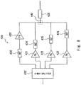
- Fig. 8 is a block diagram showing a configuration of an RF power amplifier 400 which is an example of the Doherty amplifier.
- the RF power amplifier 400 includes a carrier amplifier 420 and three peak amplifiers 421, 422, and 423.
- the peak amplifiers 421, 422, and 423 are connected to an output load 428 via 90° transformers 424, 425, and 426, respectively.
- the 90° transformer 430 connects a four-way splitter 432 to the carrier amplifier 420.
- Doherty functions can be expanded by the plurality of peak amplifiers.
- An increase by the plurality of peak amplifiers corresponding to 6 dB can be expected in the power range, and peak efficiency can be maintained for the increased power range. The efficiency is reduced to some extent due to a limited loss of an N-way splitter.
- a four-way amplifier expands an efficient power range to a theoretical value of 18 dB. As mentioned above, such an expansion is extremely important in digital communication systems that use modulation schemes in which a ratio between a peak and average power is as high as 13 dB.
- a four-way configuration provides an overall power increase of 3 dBm as compared to a conventional two-way Doherty circuit. Accordingly, an amplifier which has 120-watt-peak output can be provided by respective paths (carrier and three peak amplifiers) that each use a 30 watt transistor in the four-way Doherty configuration.
- Non-Patent Literature 1 There is a report of another example regarding peak amplifiers of a Doherty amplifier in which a plurality of amplifiers are arranged in parallel (Non-Patent Literature 1).
- Patent Literature 1 JP 2010-50986 A WO 2012/079542 A1 relates to the technological background and refers to a Doherty power amplifier comprising a bandwidth divider, a bandwidth power amplification circuit, a broadband combination bridge and a non-linear phase network.
- Non-Patent Literature 1 Junghwan Moon et al., "Highly Efficient Three-Way Saturated Doherty Amplifier With Digital Feedback Predistortion", IEEE, August 2008, IEEE MICROWAVE AND WIRELESS COMPONENTS LETTERS, VOL. 18, NO. 8, pp.539-541
- a plurality of amplifiers (the peak amplifiers 421, 422, and 423 in Fig. 8 ) are arranged in parallel, and RF signals output from the plurality of amplifiers are combined by a combining unit (a combining unit 440 in Fig. 8 ).
- the combined RF signal is output to an output load 428.
- an impedance mismatch may occur in the combining unit 440 or the output load 428 due to a manufacturing error or the like.
- the impedance mismatch causes reflected waves to be generated in the RF signals.
- the reflected waves returned to the plurality of amplifiers are reflected again. That is, the reflected waves reciprocate through transmission lines that are in subsequent stages of the outputs of the plurality of amplifiers, thereby generating standing waves.
- an influence of the standing waves increases the impedance mismatch.
- the present invention has been made in light of the above circumstances, and an object of the present invention is to reduce reflected waves of fundamental waves generated in one of or both a carrier amplifier and a peak amplifier that are connected in parallel and to match an impedance of a Doherty amplifier with a desired value.
- An aspect of the present invention is a power amplifier including a Doherty amplifier.
- the Doherty amplifier includes a carrier amplifier unit and a peak amplifier unit and amplifies an input signal.
- One of or both the carrier amplifier unit and the peak amplifier unit includes: a plurality of dividing units, in which signals propagating between first input ports and second output ports and between second input ports and first output ports of the respective plurality of dividing units have phases shifted by 90° from phases of signals propagating between the first input ports and the first output ports and between the second input ports and the second output ports of the respective plurality of dividing units; a plurality of amplifiers that receive signals that have been obtained by dividing the input signal, amplify the divided input signals that are in phase, and output the amplified input signals respectively to the first input ports of the plurality of dividing units; a combining unit that outputs a combined signal, in which the combined signal is obtained by combining a signal input to a third input port and a signal input to a fourth input port; a first
- Another aspect of the present invention is a power amplification method including steps of inputting an input signal to a Doherty amplifier, in which the Doherty amplifier includes a carrier amplifier and a peak amplifier; in one of or both the carrier amplifier and the peak amplifier, dividing the input signal and inputting divided input signals respectively to the plurality of amplifiers; combining, by a first combining and dividing unit, signals respectively from the first output ports of the plurality of dividing units, and outputting a first combined signal to a third input port of the combining unit from the first combining and dividing unit; and combining, by a second combining and dividing unit, signals respectively from the second output ports of the plurality of dividing units, and outputting a second combined signal to a fourth input port of the combining unit from the second combining and dividing unit.
- Signals are input respectively from the plurality of amplifiers via a plurality of transmission lines having the same line length to the first and second combining and dividing units.
- the present invention it is possible to reduce reflected waves of fundamental waves generated in one of or both a carrier amplifier and a peak amplifier that are connected in parallel and to match an impedance of a Doherty amplifier with a desired value.
- Fig. 8 is a block diagram showing a configuration of an RF power amplifier 400 which is an example of a Doherty amplifier.
- FIG. 1 is a block diagram schematically showing a configuration of the power amplifier 100 according to the first embodiment.
- the power amplifier 100 is configured as a power amplifier including a so-called Doherty amplifier.
- the power amplifier 100 includes a Doherty amplifier 101 and a transmission line L12
- the Doherty amplifier 101 is configured to include a carrier amplifier unit 1, a peak amplifier unit 2, a dividing unit 3, a combining unit 4, and a transmission line L11.
- both the carrier amplifier unit 1 and the peak amplifier unit 2 are used to amplify power.
- the power amplifier 100 when the power amplifier 100 operates with low power, the power amplifier 100 stops the peak amplifier unit 2, and only the carrier amplifier unit 1 is used to amplify the power.
- the power amplifier 100 can reduce power consumed by power amplification and operate highly efficiently even with an output voltage smaller than saturated power.
- the dividing unit 3 divides signals input from an input terminal Tin.
- the dividing unit 3 includes, for example, a 3 dB 90° hybrid coupler 31.
- One input port of the 3 dB 90° hybrid coupler 31 is connected to the input terminal Tin.
- An absorbing resistor R30 is connected between another input port of the 3 dB 90° hybrid coupler 31 and the ground.
- the input ports of the 3 dB 90° hybrid coupler 31 are isolated from each other.
- the outputs ports of the 3 dB 90° hybrid coupler 31 are isolated from each other.
- the dividing unit 3 equally divides the RF signal RF and outputs equally divided RF signals (denoted by 1/2RF in Fig. 1 ) respectively to the carrier amplifier unit 1 and the peak amplifier unit 2.
- the dividing unit 3 includes the 3 dB hybrid coupler 31, a phase difference of 90° is generated between the equally divided RF signals.
- a phase of the RF signal input to the peak amplifier unit 2 is shifted by 90° from a phase of the RF signal input to the carrier amplifier unit 1.
- the carrier amplifier unit 1 amplifies the input RF signal (1/2RF) and outputs an amplified RF signal RF1.
- the peak amplifier unit 2 amplifies the input RF signal (1/2RF) and outputs an amplified RF signal RF2.
- a phase of the RF signal input to the peak amplifier unit 2 is shifted by 90° from a phase the RF signal input to the carrier amplifier unit 1.
- a phase of the RF signal RF2 is shifted by 90° from a phase of the RF signal RF1.
- the transmission line L11 has a transmission line length of a 1/4 wavelength of the RF signal amplified by the carrier amplifier unit 1 and a characteristic impedance of 50 ⁇ .
- An output of the carrier amplifier unit 1 is connected to the combining unit 4 via the transmission line L11.
- An output of the peak amplifier unit 2 is also connected to the combining unit 4. Then, the phase of the RF signal RF1 that has passed through the transmission line L11 and the phase of the RF signal RF2 are synchronized when they are input to the combining unit 4.
- the combining unit 4 combines the RF signals RF1 and RF2, the phases of which have been synchronized.
- the RF signal combined by the combining unit 4 passes through the transmission line L12 and is output from an output terminal Tout as an RF signal RFout.
- the transmission line L12 has a transmission line length of a 1/4 wavelength of the signals amplified by the carrier amplifier unit 1 and the peak amplifier unit 2, and the transmission line L12 converts a load of 50 ⁇ into 25 ⁇ .
- an ideal impedance of a load viewed from the Doherty amplifier is Z 0 /2, which is half of a characteristic impedance Z 0 of the transmission line L11.
- the characteristic impedance Z 0 of the transmission line L11 shall be 50 ⁇
- an impedance of a load that is externally connected shall be 25 ⁇ .
- the RF signal input from the input terminal Tin is divided to the carrier amplifier unit 1 and the peak amplifier unit 2 by the hybrid coupler 31.
- the phase of the RF signal divided to the peak amplifier unit 2 is -90° with respect to the signal divided to the carrier amplifier unit 1.
- the transmission line L11 has a line length of a 1/4 wavelength and has a characteristic impedance of 50 ⁇ .
- Z Load obtained by the expression (1) is 100 ⁇ . Accordingly, when 25 ⁇ which is the load when the output side is viewed from the transmission line L11 is transformed, the load viewed from the carrier amplifier unit 1 is 100 ⁇ . That is, in this case, the carrier amplifier unit 1 operates with a load of 100 ⁇ , amplifies signals, and outputs the amplified signals.
- the carrier amplifier unit 1 and the peak amplifier unit 2 each operate with a load of 50 ⁇ to match 25 ⁇ which is the load when the output side is viewed from the transmission line L11, and outputs of the carrier amplifier unit 1 and the peak amplifier unit 2 are combined and then output.
- the Doherty amplifier 101 satisfies requirements of a Doherty amplifier for the load of 25 ⁇ .
- the transmission line L12 transforms the impedance from 50 ⁇ into 25 ⁇ . Therefore, when the output terminal Tout is viewed from the transmission line L11, the load appears to be 25 ⁇ .
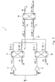
- Fig. 2 is a block diagram schematically showing a configuration of the carrier amplifier unit 1 including a plurality of amplifiers.
- the carrier amplifier unit 1 includes an amplifier 11, a dividing unit 12, a combining and dividing unit 13, an amplifier 21, a dividing unit 22, a combining and dividing unit 23, a combining unit 30, absorbing resistors R1 to R3, and transmission lines L5 and L6.
- the transmission lines L5 and L6 have the same line length.
- the line length of the transmission lines L5 and L6 can be, for example, a 1/4 wavelength of the RF signal.
- the characteristic impedance of both the transmission lines L5 and L6 in this case will be 35.4 ⁇ .
- the RF signal (1/2RF) input to the carrier amplifier unit 1 is divided (denoted by 1/4RF in Fig. 2 ), and the divided RF signals are input respectively to the amplifiers 11 and 21.
- the amplifier 11 amplifies the input RF signal (denoted by 1/4RF in Fig. 2 ) and outputs the amplified RF signal to an input port P1 of the dividing unit 12.
- the amplifier 21 amplifies the input RF signal (denoted by 1/4RF in Fig. 2 ) by the same gain and in the same phase as those of the amplifier 11. Then, the amplifier 21 outputs the amplified signal to an input port P1 of the dividing unit 22.
- the RF signals amplified by the amplifiers 11 and 21 are represented by A[0°]. Note that A represents power levels of the amplified RF signals, and [0°] represents phases of the amplified RF signals.
- the dividing unit 12 is configured as, for example, a 3 dB 90° hybrid coupler.
- the absorbing resistor R1 is connected between an input port P2 of the dividing unit 12 and the ground.
- the dividing unit 12 equally divides the RF signal A[0°] that is input to the input port P1 and outputs equally divided RF signals respectively to output ports P3 and P4. In this case, a phase of the RF signal in the output port P4 is shifted by -90° from a phase of the RF signal in the output port P3.
- the RF signal in the output port P3 is denoted by A/2[0°]
- the RF signal in the output port P4 is denoted by A/2[-90°].
- the RF signal A/2[0°] from the output port P3 of the dividing unit 12 is input to the combining and dividing unit 13.
- the RF signal A/2[-90°] from the output port P4 of the dividing unit 12 is input to the combining and dividing unit 23.
- the input ports P1 and P2 of the dividing unit 12 are isolated from each other.
- the output ports P3 and P4 of the dividing unit 12 are isolated from each other.
- the dividing unit 22 is configured as, for example, a 3 dB 90° hybrid coupler.
- the absorbing resistor R2 is connected between an input port P2 of the dividing unit 22 and the ground.
- the dividing unit 22 equally divides the RF signal A[0°] that is input to the input port P1 and outputs equally divided RF signals respectively to output ports P3 and P4. In this case, a phase of the RF signal in the output port P4 is shifted by -90° from a phase of the RF signal in the output port P3.
- the RF signal in the output port P3 is denoted by A/2[0°]
- the RF signal in the output port P4 is denoted by A/2[-90°].
- the RF signal A/2[0°] from the output port P3 of the combining and dividing unit 13 is input to the combining and dividing unit 13.
- the RF signal A/2[-90°] from the output port P4 of the combining and dividing unit 13 is input to the combining and dividing unit 23.
- the input ports P1 and P2 of the dividing unit 22 are isolated from each other.
- the output ports P3 and P4 of the dividing unit 22 are isolated from each other.
- the input ports P1 of the dividing units 12 and 22 are also referred to as first input ports.
- the input ports P2 of the dividing units 12 and 22 are also referred to as second input ports.
- the output ports P3 of the dividing units 12 and 22 are also referred to as first output ports.
- the output ports P4 of the dividing units 12 and 22 are also referred to as second output ports.
- the combining and dividing unit 13 combines the RF signal A/2[0°] from the output port P3 of the dividing unit 12 with the RF signal A/2[0°] from the output port P3 of the dividing unit 22.
- the RF signal A/2[0°] from the output port P3 of the dividing unit 12 and the RF signal A/2[0°] from the output port P3 of the dividing unit 22 are combined in phase by the combining and dividing unit 13.
- the combining and dividing unit 13 outputs a combined RF signal A[0°] to an input port P1 of the combining unit 30 via the transmission line L5.
- the combining and dividing unit 13 is also referred to as a first combining and dividing unit.
- the input port P1 of the combining unit 30 is also referred to as a third input port.
- the combining and dividing unit 23 combines the RF signal A/2[-90°] from the output port P4 of the dividing unit 12 and the RF signal A/2[-90°] from the output port P4 of the dividing unit 22.
- the RF signal A/2[-90°] from the output port P4 of the dividing unit 12 and the RF signal A/2[-90°] from the output port P4 of the dividing unit 22 are combined in phase by the combining and dividing unit 23.
- the combining and dividing unit 23 outputs a combined signal Asin( ⁇ 0 -90°) to an input port P2 of the combining unit 30 via a transmission line L6.
- the combining and dividing unit 23 is also referred to as a second combining and dividing unit.
- the input port P2 of the combining unit 30 is also referred to as a fourth input port.
- the transmission lines L5 and L6 have a line length of a 1/4 wavelength. That is, the phase of the RF signal A[0°] output from the combining and dividing unit 13 is shifted by 90° in the transmission line L5 and becomes the RF signal A[-90°]. Thus, the RF signal A[-90°] is input to the input port P1 of the combining unit 30. The phase of the RF signal A[-90°] output from the combining and dividing unit 23 is shifted by 90° in the transmission line L6 and becomes the RF signal A[-180°]. Then, the RF signal A[-180°] is input to the input port P2 of the combining unit 30. Accordingly, a phase difference between the RF signal input to the input port P1 of the combining unit 30 and the RF signal input to the input port P2 of the combining unit 30 is maintained at 90°.
- the variations in the transmission lines L5 and L6 are considered to be comparable.
- the combining unit 30 is configured as, for example, a 3 dB 90° hybrid coupler.
- the absorbing resistor R3 is connected between an output port P3 of the combining unit 30 and the ground.
- an output port P4 is connected to the transmission line L11.
- the input ports P1 and P2 of the combining unit 30 are isolated from each other.
- the output ports P3 and P4 of the combining unit 30 are isolated from each other.
- the combining unit 30 includes a 3 dB 90° hybrid coupler, when the phase difference of the RF signal input to the input port P2 with respect to the RF signal input to the input port P1 is -90°, the RF signal input to the input port P1 and the RF signal input to the input port P2 are combined, and the combined RF signal is output to the output port P4.
- the RF signal A[-90°] is input to the input port P1 of the combining unit 30
- the RF signal A[-180°] is input to the input port P2 of the combining unit 30
- the RF signals are combined, and the RF signal 2A[-180°] is output to the output port P4.
- the RF signal input to the carrier amplifier unit 1 is amplified and output as the RF signal RF1.
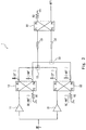
- Fig. 3 is a block diagram schematically showing a configuration of the carrier amplifier unit 1 when the reflected waves generated in the combining and dividing units 13 and 23 are displayed.
- the reflected waves for the RF signal A/2[-0°] generated in the combining and dividing unit 13 are represented by a reflected signal B/2[0°].
- the reflected waves for the RF signal A/2[-90°] generated in the combining and dividing unit 23 are represented by reflected signals B/2[-90°].
- the reflected signals B/2[0°] that are reflected by the combining and dividing unit 13 are directed to the output port P3 of the dividing unit 12 and the output port P3 of the dividing unit 22, respectively.
- the reflected signals B/2[-90°] that are reflected by the combining and dividing unit 23 are directed to the output port P4 of the dividing unit 12 and the output port P4 of the dividing unit 22, respectively.
- the dividing unit 12 includes a 3 dB 90° hybrid coupler.
- a phase difference of the reflected signal input to the output port P4 of the dividing unit 12 with respected to the reflected signal input to the output port P3 of the dividing unit 12 is -90°
- the reflected signal B/2[0°] input to the output port P3 and the reflected signal B/2[-90°] input to the output port P4 are combined and output from the input port P2, and then absorbed by the absorbing resistor R1.
- the dividing unit 22 includes a 3 dB 90° hybrid coupler.
- a phase difference of the reflected signal input to the output port P4 of the dividing unit 22 with respect to the reflected signal input to the output port P3 of the dividing unit 22 is -90°
- the reflected signal B/2[0°] input to the output port P3 and the reflected signal B/2[-90°] input to the output port P4 are combined and output from the input port P2, and then absorbed by the absorbing resistor R2.
- the loads of the amplifiers 11 and 21 need to appear to be 100 ⁇ when the load of the carrier amplifier unit 1 is 100 ⁇ (when the input signal level is low, and the peak amplifier unit 2 is stopped).
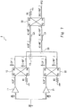
- Fig. 4 is a block diagram schematically showing a configuration of the carrier amplifier unit 1 when the reflected wave generated in the output port P4 of the combining unit 30 is displayed.
- the reflected wave for the RF signal 2A[-180°] (see Fig. 2 ) output from the output port P4 of the combining unit 30 is represented by a reflected signal C[0°].
- the reflected signal C[0°] generated in the output port P4 of the combining unit 30 is divided by the combining unit 30 and equally divided between the input ports P1 and P2 of the combining unit 30.
- a phase difference of -90° is generated in the reflected signal output to the input port P1 of the combining unit 30 with respect to the reflected signal output to the input port P2 of the combining unit 30.
- the reflected signal output to the input port P1 of the combining unit 30 is denoted by C/2[-90°]
- the reflected signal output to the input port P2 of the combining unit 30 is denoted by C/2[0°].
- the reflected signal output from the input port P1 of the combining unit 30, passes through the transmission line L5, and is input to the combining and dividing unit 13 becomes C/2[-180°].
- the reflected signal output from the input port P2 of the combining unit 30, passes through the transmission line L6, and is input to the combining and dividing unit 23 becomes C/2[-90°].
- the reflected signal C/2[-180°] input to the combining and dividing unit 13 is equally divided, and the equally divided signals C/4[-180°] are output respectively to the output port P3 of the dividing unit 12 and the output port P3 of the dividing unit 22.
- the reflected signal C/2[-90°] input to the combining and dividing unit 23 is equally divided, and equally divided signals C/4[-90°] are output respectively to the output port P4 of the dividing unit 12 and the output port P4 of the dividing unit 22.
- the RF signals output from the amplifiers 11 and 21 are A[0°], while the reflected signals returning to the amplifiers 11 and 21 are C/2[-180°].
- the RF signal output from the output port P4 of the combining unit 30 is 2A[-180°], while the reflected signal is C[0°].
- a ratio between the RF signal and the reflected signal is 2A:C for both the amplifiers 11 and 21.
- a ratio between the RF signal and the reflected signal is 180° for both the amplifiers 11 and 21.
- the loads of the amplifiers 11 and 22 can be matched with a desired impedance both in a state when the peak amplifier unit 2 is operating and in a state when the peak amplifier unit 2 is stopped.
- Fig. 5 is a block diagram schematically showing a configuration of the power amplifier 150 according to the comparative example 1.
- the power amplifier 150 is configured as a power amplifier including a so-called Doherty amplifier.
- the power amplifier 150 includes a Doherty amplifier 151 and a transmission line L12
- the Doherty amplifier 151 is configured to include a carrier amplifier unit 1501, a peak amplifier unit 1502, a dividing unit 3, a combining unit 4, and a transmission line L11.
- both the carrier amplifier unit 1501 and the peak amplifier unit 1502 are used to amplify power.
- the power amplifier 150 stops the peak amplifier unit 1502, and only the carrier amplifier unit 1501 is used to amplify the power.
- the power amplifier 150 can reduce power consumed by power amplification and operate highly efficiently even with an output voltage smaller than saturated power.
- the dividing unit 3 equally divides the RF signal RF and outputs equally divided RF signals (denoted by 1/2RF in Fig. 5 ) respectively to the carrier amplifier unit 1501 and the peak amplifier unit 1502.
- the carrier amplifier unit 1501 amplifies the input RF signal (1/2RF) and outputs an amplified RF signal RF1.
- the peak amplifier unit 1502 amplifies the input RF signal (1/2RF) and outputs an amplified RF signal RF2.
- the power amplifier 150 as a mechanism in which the RF signals RF1 and RF2 are combined by the combining unit 4 and then output from the output terminal Tout via the transmission line L12 is the same as that in the power amplifier 100, a description of such a mechanism will be omitted.
- Fig. 6 is a block diagram schematically showing a configuration of the carrier amplifier unit 1501 including a plurality of amplifiers.
- the carrier amplifier unit 1501 includes amplifiers 1511 and 1521, a combining and dividing unit 1513, and a transmission line L153.
- the amplifiers 1511 and 1521 of the carrier amplifier unit 1501 are a class A or biased class AB.
- the RF signal (1/2RF) input to the carrier amplifier unit 1501 is divided (denoted by 1/4RF in Fig. 6 ) and divided RF signals are input respectively to the amplifiers 1511 and 1521.
- the amplifier 1511 amplifies the input RF signal (denoted by 1/4RF in Fig. 6 ).
- the signal amplified by the amplifier 1511 is transmitted to the combining and dividing unit 1513.
- the amplifier 1521 amplifies the input RF signal (denoted by 1/4RF in Fig. 6 ) by the same gain as that of the amplifier 1511.
- the signal amplified by the amplifier 1521 is transmitted to the combining and dividing unit 1513.
- the RF signals amplified by the amplifiers 1511 and 1521 are represented by A[0°].
- A represents a power level of the RF signal
- [0°] represents a phase of the RF signal.
- phases of the RF signals at output terminals of the amplifiers 1511 and 1521 are used as a reference, they are denoted by 0°.
- the RF signal A[0°] from the amplifier 1511 and the RF signal A[0°] from the amplifier 1521 are combined in phase by the combining and dividing unit 1513.
- the RF signal (denoted by 2A[0°] in Fig. 6 ) combined by the combining and dividing unit 1513 passes through the transmission line L153, becomes the RF signal RF1, and is output to the transmission line L11 from the carrier amplifier unit 1501.
- the transmission line L153 has a transmission line length of a 1/4 wavelength of the signal amplified by the carrier amplifier unit 1, and the transmission line L153 converts a load of 50 ⁇ into 25 ⁇ .
- the power amplifier 150 is manufactured in such a way that an impedance when the transmission line L153 is viewed from the combining and dividing unit 1513 appears to be 25 ⁇ .
- an impedance when the transmission line L153 is viewed from the combining and dividing unit 1513 appears to be 25 ⁇ .
- the amplifiers 1511 and 1521 cannot be matched with a desired load 50 ⁇ .
- a reflected wave is generated in the combining and dividing unit 1513.
- a part of the reflected wave reaches an output of the amplifier 1511.
- the output of the amplifier 1511 is high impedance
- the reflected wave that has reached the output of the amplifier 1511 is reflected again.
- the reflected wave reaches an output of the amplifier 1521.
- the output of the amplifier 1521 is high impedance
- the reflected wave that has reached the output of the amplifier 1521 is reflected again.
- the reflected wave generated in the combining and dividing unit 1513 reciprocates inside the Doherty amplifier 151, thereby generating standing waves.
- the impedances of the transmission lines disposed in the power amplifier 150 deviate, and this causes a problem in an operation of the Doherty amplifier.
- the impedance of the transmission line L11 viewed from the carrier amplifier unit 1501 is 50 ⁇ .
- the impedance of the transmission line L11 viewed from the carrier amplifier unit 1501 appears to be 100 ⁇ . Therefore, when only the carrier amplifier unit 1501 performs an amplification operation, the deviation in the impedances of the transmission lines caused by the standing waves has a particularly large influence.
- the amplifiers 1511 and 1512 are manufactured in such a way that their output levels will become the same. However, in practice, there are variations in output levels of the amplifiers 1511 and 1512 due to a manufacturing error or the like. In such a case, some of the RF signals output from one of the amplifiers having a great output level pass through the combining and dividing unit 1513 and reach the other one of the amplifiers, which is a state in which isolation is insufficient. When the amplifiers 1511 and 1512 are biased class C amplifiers, the output levels of the amplifiers 1511 and 1512 are likely to vary, which is particularly problematic. Even in such a case, as the RF signals that have reached the outputs of the amplifiers are reflected, these cause the standing waves to be generated in a manner similar to the reflected waves that cause the standing waves to be generated.
- the power amplifier 150 according to the comparative example 1 cannot reduce the influence of the standing waves generated inside the Doherty amplifier and the loads of the amplifiers cannot be matched with the desired impedance.
- the dividing unit 12 that is at a subsequent stage of the amplifier 11 can absorb RF signals that leak due to the reflected waves and insufficient isolation.
- the dividing unit 22 that is at a subsequent stage of the amplifier 21 can absorb RF signals that leak due to the reflected waves and insufficient isolation. Consequently, the standing waves will not be generated, thereby preventing deviation of the impedances of the transmission lines. That is, the power amplifier 100 can prevent the standing waves in the Doherty amplifier when a plurality of amplifiers are arranged in parallel in one of or both the carrier amplifier unit 1 and the peak amplifier unit 2.
- the power amplifier 200 has the same configuration as that of the power amplifier 100 shown in Fig. 1 .
- the power amplifier 200 is configured in such a way that the peak amplifier unit 2 includes a plurality of amplifiers.
- the configuration of the power amplifier 200 other than the peak amplifier unit 2 is the same as that of the power amplifier 100, a description of the configuration of the power amplifier 200 other than the peak amplifier unit 2 will be omitted.
- Fig. 7 is a block diagram schematically showing a configuration of the peak amplifier unit 2 of the power amplifier 200 according to the second embodiment. As shown in Fig. 7 , the peak amplifier unit 2 of the power amplifier 200 can have the same configuration as that of the peak amplifier unit 2 of the power amplifier 100.
- a power amplifier capable of reducing or preventing reflected waves of fundamental waves generated when amplifiers are operated in parallel inside a Doherty amplifier and capable of matching loads of the amplifiers with a desired impedance can be achieved.
- the present invention is not limited to the above embodiments, and modifications can be made without departing from the scope of the invention as appropriate.
- the reflection factors of the RF signals in the input ports P1 and P2 of the combining unit 30 are comparable, it is not limited to this. That is, the reflection factors of the RF signals in the input ports P1 and P2 of the combining unit 30 are not necessarily comparable.
- the dividing units 12 and 22 equally divide signals input to the input ports P1 and P2 and the output ports P3 and P4, it is not limited to this.
- the dividing units 12 and 22 cannot be prevented from dividing the signals input to the input ports P1 and P2 and the output ports P3 and P4 by a ratio other than an equal division.
- the combining and dividing units 13 and 23 equally divide the reflected waves returned from the combining unit 30, it is not limited to this. That is, the combining and dividing units 13 and 23 cannot be prevented from dividing the reflected signals returned from the combining unit 30 by a ratio other than an equal division. In this case, components that cannot be cancelled remain in the reflected signals in the input ports P1 of the dividing units 12 and 22.
- the power amplifier according to the above embodiments can exert an effect of reducing the reflected waves.
- dividers 12 and 22 and the combining unit 30 are 3 dB 90° hybrid couplers
- Other dividers may be incorporated as long as they are dividers having two inputs and two outputs, can divide (or equally divide) signals that are input from the respective inputs into two outputs, and can provide a phase difference of 90° to the divided signals.
- the carrier amplifier unit and the peak amplifier unit 2 including two amplifiers and dividers
- the carrier amplifier unit and the peak amplifier unit including n (n is an integer greater or equal to three) amplifiers and dividers may be included.
- signals each having a phase of [0°] that are output from the n amplifier(s) may be combined by a combining and dividing unit having n input(s) and one output, and then the combined signal may be output to the input port P1 of the combining unit 30.
- signals each having a phase of [-90°] that are output from the n amplifier(s) may be combined by the combining and dividing unit having n input(s) and one output, and then the combined signal may be output to the input port P2 of the combining unit 30.
- a power amplifier that can reduce reflected waves can be achieved.
- impedance conversion by the transmission lines L5 and L6 has been described, it is merely illustrative.
- it may be configured in such a way that other transmission lines may be provided respectively between the transmission line L5 and the output port P3 of the dividing unit 12, between the transmission line L5 and the output port P3 of the dividing unit 22, between the transmission line L6 and the output port P4 of the dividing unit 12, and between the transmission line L6 and the output port P4 of the dividing unit 22.
- the transmission line provided between the transmission line L5 and the output port P3 of the dividing unit 12 will be referred to as a transmission line L1.
- the transmission line provided between the transmission line L5 and the output port P3 of the dividing unit 22 will be referred to as a transmission line L3.
- the transmission line provided between the transmission line L6 and the output port P4 of the dividing unit 12 will be referred to as a transmission line L2.
- the transmission line provided between the transmission line L6 and the output port P4 of the dividing unit 22 will be referred to as a transmission line L4.
- Line lengths of the transmission lines L1 to L4 are a 1/4 wavelength.
- impedance conversion by the transmission lines L7 and L8 is 35 ⁇ .
- an impedance when the combining and dividing unit 13 is viewed from the transmission lines L1 and L3 is 70 ⁇ .
- An impedance when the combining and dividing unit 23 is viewed from the transmission lines L2 and L4 is 70 ⁇ .
- two stages of impedance conversion which includes impedance conversion by the transmission lines L1 and L3 and the impedance conversion by the transmission line L7, is performed.
- two stages of impedance conversion which includes impedance conversion by the transmission lines L2 and L4 and the impedance conversion by the transmission line L8, is performed. Then, as impedance conversion can be gradually performed in each of the stages, a Doherty amplifier operating in a wider frequency band can be achieved.
- the power amplifier according to the above embodiments can be used by various communication systems such as a radio communication system.
Landscapes
- Engineering & Computer Science (AREA)
- Power Engineering (AREA)
- Amplifiers (AREA)
Claims (12)
- Leistungsverstärker (100), der einen Doherty-Verstärker (101) aufweist, wobei der Doherty-Verstärker (101) eine Trägerverstärkereinheit (1) und eine Spitzenverstärkereinheit (2) aufweist und konfiguriert ist, ein Eingangssignal zu verstärken, wobei eine oder beide der Trägerverstärkereinheit (1) und der Spitzenverstärkereinheit (2) aufweisen:eine Vielzahl von Aufteilungseinheiten (12, 22), wobei Signale, die sich zwischen ersten Eingangsanschlüssen (P1) und zweiten Ausgangsanschlüssen (P4) und zwischen zweiten Eingangsanschlüssen (P2) und ersten Ausgangsanschlüssen (P3) der jeweiligen Vielzahl der Aufteilungseinheiten (12, 22) ausbreiten, Phasen aufweisen, die um 90° zu den Phasen der Signale verschoben sind, die sich zwischen den ersten Eingangsanschlüssen (P1) und den ersten Ausgangsanschlüssen (P3) und zwischen den zweiten Eingangsanschlüssen (P2) und den zweiten Ausgangsanschlüssen (P4) der jeweiligen Vielzahl der Aufteilungseinheiten (12, 22) ausbreiten;eine Vielzahl von Verstärkern, die konfiguriert sind, Signale zu empfangen, die durch Aufteilen des Eingangssignals erhalten worden sind, die aufgeteilten Eingangssignale zu verstärken, die in Phase sind, und die verstärkten Eingangssignale jeweils an die ersten Eingangsanschlüsse (P1) der Vielzahl der Aufteilungseinheiten (12, 22) abzugeben;eine Kombinationseinheit (4, 30), die konfiguriert ist, ein kombiniertes Signal abzugeben, wobei das kombinierte Signal durch Kombinieren eines Signals, das in einen dritten Eingangsanschluss eingegeben wird, und eines Signals erhalten wird, das in einen vierten Eingangsanschluss eingegeben wird;eine erste Kombinations- und Aufteilungseinheit (13), die konfiguriert ist, ein erstes kombiniertes Signal an den dritten Eingangsanschluss der Kombinationseinheit (4, 30) abzugeben, wobei das erste kombinierte Signal durch Kombinieren von Signalen aus den ersten Ausgangsanschlüssen (P3) der jeweiligen Vielzahl der Aufteilungseinheiten (12, 22) erhalten wird;eine zweite Kombinations- und Aufteilungseinheit (23), die konfiguriert ist, ein zweites kombiniertes Signal an den vierten Eingangsanschluss der Kombinationseinheit (4, 30) abzugeben, wobei das zweite kombinierte Signal durch Kombinieren von Signalen aus den zweiten Ausgangsanschlüssen (P4) der jeweiligen Vielzahl der Aufteilungseinheiten (12, 22) erhalten wird; undeine Vielzahl von Übertragungsleitungen (L11, L12), die konfiguriert sind, die Vielzahl der Verstärker jeweils mit den ersten und zweiten Kombinations- und Aufteilungseinheiten (13, 23) durch dieselbe Leitungslänge zu verbinden.
- Leistungsverstärker (100) nach Anspruch 1, wobei die Aufteilungseinheit ein 3 dB-90°-Hybridkoppler ist, der zwei Eingänge und zwei Ausgänge aufweist.
- Leistungsverstärker (100) nach Anspruch 1 oder 2, wobei zwischen dem zweiten Eingangsanschluss der Aufteilungseinheit und einer Massespannung ein Widerstand geschaltet ist.
- Leistungsverstärker (100) nach einem der Ansprüche 1 bis 3, wobei das Eingangssignal gleichmäßig aufgeteilt wird, und die Vielzahl der Verstärker konfiguriert ist, jeweils gleichmäßig aufgeteilte Eingangssignale zu empfangen.
- Leistungsverstärker (100) nach einem der Ansprüche 1 bis 4, wobei die erste Kombinations- und Aufteilungseinheit (13) konfiguriert ist, ein erstes reflektiertes Signal aus einem Ausgang der Kombinationseinheit (4, 30) aufzuteilen und aufgeteilte erste reflektierte Signale jeweils an die ersten Ausgangsanschlüsse (P3) der Vielzahl der Aufteilungseinheiten (12, 22) abzugeben, und
die zweite Kombinations- und Aufteilungseinheit (23) konfiguriert ist, ein zweites reflektiertes Signal aus dem Ausgang der Kombinationseinheit (4, 30) aufzuteilen und aufgeteilte zweite reflektierte Signale jeweils an die zweiten Ausgangsanschlüsse (P4) der Vielzahl der Aufteilungseinheiten (12, 22) abzugeben. - Leistungsverstärker (100) nach Anspruch 5, wobei die Kombinationseinheit (4, 30) konfiguriert ist, Phasen von Signalen, die sich zwischen dem dritten Eingangsanschluss und einem vierten Ausgangsanschluss und zwischen den vierten Eingangsanschluss und einen dritten Ausgangsanschluss ausbreiten, gegenüber Phasen von Signalen um 90° zu verschieben, die sich zwischen dem dritten Eingangsanschluss und dem dritten Ausgangsanschluss und zwischen dem vierten Eingangsanschluss und dem vierten Ausgangsanschluss ausbreiten.
- Leistungsverstärker (100) nach Anspruch 6, wobei die Kombinationseinheit (4, 30) ein 3 dB-90°-Hybridkoppler ist, der zwei Eingänge und zwei Ausgänge aufweist.
- Leistungsverstärker (100) nach einem der Ansprüche 5 bis 7, wobei die erste Kombinations- und Aufteilungseinheit (13) konfiguriert ist, das erste reflektierte Signal gleichmäßig aufzuteilen und gleichmäßig aufgeteilte erste reflektierte Signale jeweils an die ersten Ausgangsanschlüsse (P3) der Vielzahl der Aufteilungseinheiten (12, 22) abzugeben, und
die zweite Kombinations- und Aufteilungseinheit (23) konfiguriert ist, das zweite reflektierte Signal gleichmäßig aufzuteilen und gleichmäßig aufgeteilte zweite reflektiertes Signale jeweils an die zweiten Ausgangsanschlüsse (P4) der Vielzahl der Aufteilungseinheiten (12, 22) abzugeben. - Leistungsverstärker (100) nach einem der Ansprüche 1 bis 8, wobei die Vielzahl der Übertragungsleitungen (L11, L12) jeweils eine Leitungslänge einer 1/4 Wellenform eines Signals aufweist, das dort hindurch übertragen werden soll.
- Leistungsverstärker (100) nach einem der Ansprüche 1 bis 9, wobei die Vielzahl der Verstärker dieselbe Verstärkung aufweist.
- Leistungsverstärker (100) nach einem der Ansprüche 1 bis 10, der ferner aufweist:einen Impedanzwandler, der zwischen einen Ausgängen der Trägerverstärkereinheit (1) und der Spitzenverstärkereinheit (2) und an Ausgangsanschluss vorgesehen ist; undeine erste Übertragungsleitung, die zwischen anderen Ausgängen der Trägerverstärkereinheit (1) und der Spitzenverstärkereinheit (2) und dem Impedanzwandler vorgesehen ist und eine Leitungslänge mit einer 1/4 Wellenlänge eines Signals aufweist, das dort hindurch übertragen werden soll, wobeidas Eingangssignal, das eine um 90° verschobene Phase aufweist, in eine der Trägerverstärkereinheit (1) und der Spitzenverstärkereinheit (2) eingegeben wird, deren Ausgang nicht mit der ersten Übertragungsleitung verbunden ist.
- Leistungsverstärkungsverfahre, das die Schritte aufweist:Eingeben eines Eingangssignals in einen Doherty-Verstärker (101), wobei der Doherty-Verstärker (101) einen Trägerverstärker und einen Spitzenverstärker aufweist;in einen oder beide des Trägerverstärkers und des Spitzenverstärkers Aufteilen des Eingangssignals und Eingeben der aufgeteilten Eingangssignale jeweils in die Vielzahl der Verstärker;Kombinieren durch eine erste Kombinations- und Aufteilungseinheit (13) von jeweiligen Signalen aus den ersten Ausgangsanschlüssen (P3) der Vielzahl der Aufteilungseinheiten (12, 22) und Abgeben eines ersten kombinierten Signals an einen dritten Eingangsanschluss der Kombinationseinheit (4, 30) aus der ersten Kombinations- und Aufteilungseinheit; undKombinieren durch eine zweite Kombinations- und Aufteilungseinheit (23) von jeweiligen Signalen aus den zweiten Ausgangsanschlüssen (P4) der Vielzahl der Aufteilungseinheiten (12, 22), und Abgeben eines zweiten kombinierten Signals an einen vierten Eingangsanschluss der Kombinationseinheit (4, 30) aus der zweiten Kombinations- und Aufteilungseinheit, wobeiSignale jeweils aus der Vielzahl der Verstärker über eine Vielzahl von Übertragungsleitungen (L11, L12), die dieselbe Länge aufweisen, in die erste und zweite Kombinations- und Aufteilungseinheit (13, 23) eingegeben werden.
Priority Applications (1)
| Application Number | Priority Date | Filing Date | Title |
|---|---|---|---|
| HUE13897535A HUE042002T2 (hu) | 2013-11-14 | 2013-11-14 | Teljesítményerõsítõ és teljesítményerõsítési eljárás |
Applications Claiming Priority (1)
| Application Number | Priority Date | Filing Date | Title |
|---|---|---|---|
| PCT/JP2013/006691 WO2015071931A1 (ja) | 2013-11-14 | 2013-11-14 | 電力増幅器及び電力増幅方法 |
Publications (3)
| Publication Number | Publication Date |
|---|---|
| EP3070840A1 EP3070840A1 (de) | 2016-09-21 |
| EP3070840A4 EP3070840A4 (de) | 2017-07-19 |
| EP3070840B1 true EP3070840B1 (de) | 2018-10-31 |
Family
ID=53056903
Family Applications (1)
| Application Number | Title | Priority Date | Filing Date |
|---|---|---|---|
| EP13897535.4A Active EP3070840B1 (de) | 2013-11-14 | 2013-11-14 | Leistungsverstärker und leistungsverstärkungsverfahren |
Country Status (5)
| Country | Link |
|---|---|
| US (1) | US9673761B2 (de) |
| EP (1) | EP3070840B1 (de) |
| JP (1) | JP6176333B2 (de) |
| HU (1) | HUE042002T2 (de) |
| WO (1) | WO2015071931A1 (de) |
Families Citing this family (8)
| Publication number | Priority date | Publication date | Assignee | Title |
|---|---|---|---|---|
| EP3316479B1 (de) * | 2015-07-28 | 2022-10-26 | Huawei Technologies Co., Ltd. | Leistungsverstärker, leistungsverstärkungsverfahren sowie steuerungsvorrichtung und -verfahren für leistungsverstärker |
| EP3346607B1 (de) * | 2015-09-01 | 2021-03-17 | Nec Corporation | Leistungsverstärkungsvorrichtung und fernsehsignalübertragungssystem |
| US10418947B2 (en) * | 2017-03-01 | 2019-09-17 | Sumitomo Electric Device Innovations, Inc. | Doherty amplifier |
| US10432147B2 (en) | 2017-03-01 | 2019-10-01 | Sumitomo Electric Device Innovations, Inc. | Inverted three-stage Doherty amplifier |
| CN109450484B (zh) * | 2018-11-30 | 2020-04-14 | 普联技术有限公司 | 一种信号反射消除电路及方法 |
| CN110086440A (zh) * | 2019-04-25 | 2019-08-02 | 成都中宇微芯科技有限公司 | 超宽带一分四开关放大器及开关放大器系统 |
| EP4024704A4 (de) * | 2019-09-16 | 2022-08-31 | Huawei Technologies Co., Ltd. | Leistungsverstärkerschaltung, sender und netzwerkvorrichtung |
| WO2023238185A1 (ja) * | 2022-06-06 | 2023-12-14 | 日本電信電話株式会社 | 合波器 |
Family Cites Families (15)
| Publication number | Priority date | Publication date | Assignee | Title |
|---|---|---|---|---|
| US6700444B2 (en) | 2002-01-28 | 2004-03-02 | Cree Microwave, Inc. | N-way RF power amplifier with increased backoff power and power added efficiency |
| US6791417B2 (en) * | 2002-01-28 | 2004-09-14 | Cree Microwave, Inc. | N-way RF power amplifier circuit with increased back-off capability and power added efficiency using selected phase lengths and output impedances |
| US8180303B2 (en) * | 2008-05-28 | 2012-05-15 | Hollinworth Fund, L.L.C. | Power amplifier architectures |
| JP5243192B2 (ja) * | 2008-11-12 | 2013-07-24 | 株式会社日立国際電気 | 増幅器 |
| KR101097605B1 (ko) * | 2009-11-04 | 2011-12-22 | 알.에프 에이치아이씨 주식회사 | 도허티 증폭기 |
| KR101709347B1 (ko) * | 2009-12-16 | 2017-03-09 | 삼성전자주식회사 | 결합셀 도허티 전력 증폭 장치 및 방법 |
| JP2011188269A (ja) | 2010-03-09 | 2011-09-22 | Mitsubishi Electric Corp | 高出力電力増幅器 |
| US8314654B2 (en) * | 2010-05-17 | 2012-11-20 | Alcatel Lucent | Multi-band high-efficiency Doherty amplifier |
| EP2403135B1 (de) * | 2010-06-24 | 2013-12-11 | Alcatel Lucent | Leistungsverstärker für mobile Telekommunikation |
| CN102142812B (zh) * | 2010-12-17 | 2013-08-28 | 华为技术有限公司 | Doherty功率放大器 |
| JP5678768B2 (ja) | 2011-03-30 | 2015-03-04 | 日本電気株式会社 | 増幅装置 |
| EP2608400B1 (de) * | 2011-12-20 | 2014-08-13 | Nxp B.V. | N-Weg-Doherty-Verstärker |
| JP2013172174A (ja) | 2012-02-17 | 2013-09-02 | Nec Corp | 電力増幅器及び送信システム |
| US9397617B2 (en) * | 2013-06-25 | 2016-07-19 | Rf Micro Devices, Inc. | Multi-broadband Doherty power amplifier |
| US9484865B2 (en) * | 2013-09-30 | 2016-11-01 | Qorvo Us, Inc. | Reconfigurable load modulation amplifier |
-
2013
- 2013-11-14 HU HUE13897535A patent/HUE042002T2/hu unknown
- 2013-11-14 WO PCT/JP2013/006691 patent/WO2015071931A1/ja active Application Filing
- 2013-11-14 JP JP2015547285A patent/JP6176333B2/ja active Active
- 2013-11-14 EP EP13897535.4A patent/EP3070840B1/de active Active
- 2013-11-14 US US15/031,795 patent/US9673761B2/en active Active
Non-Patent Citations (1)
| Title |
|---|
| None * |
Also Published As
| Publication number | Publication date |
|---|---|
| JPWO2015071931A1 (ja) | 2017-03-09 |
| EP3070840A1 (de) | 2016-09-21 |
| US20160248383A1 (en) | 2016-08-25 |
| HUE042002T2 (hu) | 2019-06-28 |
| EP3070840A4 (de) | 2017-07-19 |
| US9673761B2 (en) | 2017-06-06 |
| JP6176333B2 (ja) | 2017-08-09 |
| WO2015071931A1 (ja) | 2015-05-21 |
Similar Documents
| Publication | Publication Date | Title |
|---|---|---|
| EP3070840B1 (de) | Leistungsverstärker und leistungsverstärkungsverfahren | |
| EP2312746B1 (de) | Verstärkerschaltung für endgültige dreiweg-leistung-synthetisierung in einem systemleistungsverstärker für eine mobilkommunikationsbasisstation | |
| CN107112953B (zh) | 用于放大射频信号的功率放大器 | |
| US10218315B2 (en) | Doherty amplifier | |
| US9899962B2 (en) | Power amplifier | |
| US9252722B2 (en) | Enhanced and versatile N-way doherty power amplifier | |
| US8305141B2 (en) | Distributed Doherty power amplifier | |
| EP3461000B1 (de) | Doherty-verstärker | |
| JP6345916B2 (ja) | 増幅装置、送信装置 | |
| US10804856B2 (en) | Power amplifier | |
| US20140152389A1 (en) | Actively Tuned Circuit Having Parallel Carrier and Peaking Paths | |
| EP3700087B1 (de) | Doherty-verstärker und doherty-verstärkerschaltung | |
| KR20130123305A (ko) | 도허티 증폭기 | |
| JP2013172174A (ja) | 電力増幅器及び送信システム | |
| WO2022041286A1 (zh) | 一种Doherty功率放大器、印刷电路板及基站 | |
| KR101094067B1 (ko) | 클래스 f 및 인버스 클래스 f 도허티 증폭기 | |
| WO2012002407A1 (ja) | 高周波電力増幅器 | |
| WO2016149904A1 (zh) | 功率放大设备 | |
| Rawat et al. | Design strategy for tri-band Doherty power amplifier | |
| JP2012205018A (ja) | 高出力電力増幅器 | |
| KR100983517B1 (ko) | 기지국 출력 향상을 위한 고출력 파워엠프 | |
| CN112771778A (zh) | 功率放大器电路 | |
| JP2005086447A (ja) | 電力合成形増幅器 | |
| RU51807U1 (ru) | Многоканальное широкополосное усилительное устройство |
Legal Events
| Date | Code | Title | Description |
|---|---|---|---|
| PUAI | Public reference made under article 153(3) epc to a published international application that has entered the european phase |
Free format text: ORIGINAL CODE: 0009012 |
|
| 17P | Request for examination filed |
Effective date: 20160613 |
|
| AK | Designated contracting states |
Kind code of ref document: A1 Designated state(s): AL AT BE BG CH CY CZ DE DK EE ES FI FR GB GR HR HU IE IS IT LI LT LU LV MC MK MT NL NO PL PT RO RS SE SI SK SM TR |
|
| AX | Request for extension of the european patent |
Extension state: BA ME |
|
| DAX | Request for extension of the european patent (deleted) | ||
| A4 | Supplementary search report drawn up and despatched |
Effective date: 20170619 |
|
| RIC1 | Information provided on ipc code assigned before grant |
Ipc: H03F 3/24 20060101ALI20170612BHEP Ipc: H03F 3/189 20060101ALI20170612BHEP Ipc: H03F 1/07 20060101AFI20170612BHEP |
|
| GRAP | Despatch of communication of intention to grant a patent |
Free format text: ORIGINAL CODE: EPIDOSNIGR1 |
|
| INTG | Intention to grant announced |
Effective date: 20180514 |
|
| GRAS | Grant fee paid |
Free format text: ORIGINAL CODE: EPIDOSNIGR3 |
|
| GRAA | (expected) grant |
Free format text: ORIGINAL CODE: 0009210 |
|
| AK | Designated contracting states |
Kind code of ref document: B1 Designated state(s): AL AT BE BG CH CY CZ DE DK EE ES FI FR GB GR HR HU IE IS IT LI LT LU LV MC MK MT NL NO PL PT RO RS SE SI SK SM TR |
|
| REG | Reference to a national code |
Ref country code: CH Ref legal event code: EP Ref country code: GB Ref legal event code: FG4D |
|
| REG | Reference to a national code |
Ref country code: AT Ref legal event code: REF Ref document number: 1060612 Country of ref document: AT Kind code of ref document: T Effective date: 20181115 |
|
| REG | Reference to a national code |
Ref country code: DE Ref legal event code: R096 Ref document number: 602013046157 Country of ref document: DE |
|
| REG | Reference to a national code |
Ref country code: IE Ref legal event code: FG4D |
|
| REG | Reference to a national code |
Ref country code: NL Ref legal event code: MP Effective date: 20181031 |
|
| REG | Reference to a national code |
Ref country code: LT Ref legal event code: MG4D |
|
| REG | Reference to a national code |
Ref country code: AT Ref legal event code: MK05 Ref document number: 1060612 Country of ref document: AT Kind code of ref document: T Effective date: 20181031 |
|
| PG25 | Lapsed in a contracting state [announced via postgrant information from national office to epo] |
Ref country code: LT Free format text: LAPSE BECAUSE OF FAILURE TO SUBMIT A TRANSLATION OF THE DESCRIPTION OR TO PAY THE FEE WITHIN THE PRESCRIBED TIME-LIMIT Effective date: 20181031 Ref country code: PL Free format text: LAPSE BECAUSE OF FAILURE TO SUBMIT A TRANSLATION OF THE DESCRIPTION OR TO PAY THE FEE WITHIN THE PRESCRIBED TIME-LIMIT Effective date: 20181031 Ref country code: HR Free format text: LAPSE BECAUSE OF FAILURE TO SUBMIT A TRANSLATION OF THE DESCRIPTION OR TO PAY THE FEE WITHIN THE PRESCRIBED TIME-LIMIT Effective date: 20181031 Ref country code: AT Free format text: LAPSE BECAUSE OF FAILURE TO SUBMIT A TRANSLATION OF THE DESCRIPTION OR TO PAY THE FEE WITHIN THE PRESCRIBED TIME-LIMIT Effective date: 20181031 Ref country code: BG Free format text: LAPSE BECAUSE OF FAILURE TO SUBMIT A TRANSLATION OF THE DESCRIPTION OR TO PAY THE FEE WITHIN THE PRESCRIBED TIME-LIMIT Effective date: 20190131 Ref country code: IS Free format text: LAPSE BECAUSE OF FAILURE TO SUBMIT A TRANSLATION OF THE DESCRIPTION OR TO PAY THE FEE WITHIN THE PRESCRIBED TIME-LIMIT Effective date: 20190228 Ref country code: ES Free format text: LAPSE BECAUSE OF FAILURE TO SUBMIT A TRANSLATION OF THE DESCRIPTION OR TO PAY THE FEE WITHIN THE PRESCRIBED TIME-LIMIT Effective date: 20181031 Ref country code: NO Free format text: LAPSE BECAUSE OF FAILURE TO SUBMIT A TRANSLATION OF THE DESCRIPTION OR TO PAY THE FEE WITHIN THE PRESCRIBED TIME-LIMIT Effective date: 20190131 Ref country code: LV Free format text: LAPSE BECAUSE OF FAILURE TO SUBMIT A TRANSLATION OF THE DESCRIPTION OR TO PAY THE FEE WITHIN THE PRESCRIBED TIME-LIMIT Effective date: 20181031 |
|
| PG25 | Lapsed in a contracting state [announced via postgrant information from national office to epo] |
Ref country code: AL Free format text: LAPSE BECAUSE OF FAILURE TO SUBMIT A TRANSLATION OF THE DESCRIPTION OR TO PAY THE FEE WITHIN THE PRESCRIBED TIME-LIMIT Effective date: 20181031 Ref country code: GR Free format text: LAPSE BECAUSE OF FAILURE TO SUBMIT A TRANSLATION OF THE DESCRIPTION OR TO PAY THE FEE WITHIN THE PRESCRIBED TIME-LIMIT Effective date: 20190201 Ref country code: SE Free format text: LAPSE BECAUSE OF FAILURE TO SUBMIT A TRANSLATION OF THE DESCRIPTION OR TO PAY THE FEE WITHIN THE PRESCRIBED TIME-LIMIT Effective date: 20181031 Ref country code: RS Free format text: LAPSE BECAUSE OF FAILURE TO SUBMIT A TRANSLATION OF THE DESCRIPTION OR TO PAY THE FEE WITHIN THE PRESCRIBED TIME-LIMIT Effective date: 20181031 Ref country code: NL Free format text: LAPSE BECAUSE OF FAILURE TO SUBMIT A TRANSLATION OF THE DESCRIPTION OR TO PAY THE FEE WITHIN THE PRESCRIBED TIME-LIMIT Effective date: 20181031 Ref country code: PT Free format text: LAPSE BECAUSE OF FAILURE TO SUBMIT A TRANSLATION OF THE DESCRIPTION OR TO PAY THE FEE WITHIN THE PRESCRIBED TIME-LIMIT Effective date: 20190301 |
|
| REG | Reference to a national code |
Ref country code: HU Ref legal event code: AG4A Ref document number: E042002 Country of ref document: HU Ref country code: CH Ref legal event code: PL |
|
| PG25 | Lapsed in a contracting state [announced via postgrant information from national office to epo] |
Ref country code: DK Free format text: LAPSE BECAUSE OF FAILURE TO SUBMIT A TRANSLATION OF THE DESCRIPTION OR TO PAY THE FEE WITHIN THE PRESCRIBED TIME-LIMIT Effective date: 20181031 Ref country code: IT Free format text: LAPSE BECAUSE OF FAILURE TO SUBMIT A TRANSLATION OF THE DESCRIPTION OR TO PAY THE FEE WITHIN THE PRESCRIBED TIME-LIMIT Effective date: 20181031 Ref country code: CZ Free format text: LAPSE BECAUSE OF FAILURE TO SUBMIT A TRANSLATION OF THE DESCRIPTION OR TO PAY THE FEE WITHIN THE PRESCRIBED TIME-LIMIT Effective date: 20181031 Ref country code: LU Free format text: LAPSE BECAUSE OF NON-PAYMENT OF DUE FEES Effective date: 20181114 |
|
| REG | Reference to a national code |
Ref country code: DE Ref legal event code: R097 Ref document number: 602013046157 Country of ref document: DE |
|
| REG | Reference to a national code |
Ref country code: BE Ref legal event code: MM Effective date: 20181130 |
|
| REG | Reference to a national code |
Ref country code: IE Ref legal event code: MM4A |
|
| PG25 | Lapsed in a contracting state [announced via postgrant information from national office to epo] |
Ref country code: MC Free format text: LAPSE BECAUSE OF FAILURE TO SUBMIT A TRANSLATION OF THE DESCRIPTION OR TO PAY THE FEE WITHIN THE PRESCRIBED TIME-LIMIT Effective date: 20181031 Ref country code: LI Free format text: LAPSE BECAUSE OF NON-PAYMENT OF DUE FEES Effective date: 20181130 Ref country code: RO Free format text: LAPSE BECAUSE OF FAILURE TO SUBMIT A TRANSLATION OF THE DESCRIPTION OR TO PAY THE FEE WITHIN THE PRESCRIBED TIME-LIMIT Effective date: 20181031 Ref country code: EE Free format text: LAPSE BECAUSE OF FAILURE TO SUBMIT A TRANSLATION OF THE DESCRIPTION OR TO PAY THE FEE WITHIN THE PRESCRIBED TIME-LIMIT Effective date: 20181031 Ref country code: SM Free format text: LAPSE BECAUSE OF FAILURE TO SUBMIT A TRANSLATION OF THE DESCRIPTION OR TO PAY THE FEE WITHIN THE PRESCRIBED TIME-LIMIT Effective date: 20181031 Ref country code: CH Free format text: LAPSE BECAUSE OF NON-PAYMENT OF DUE FEES Effective date: 20181130 Ref country code: SK Free format text: LAPSE BECAUSE OF FAILURE TO SUBMIT A TRANSLATION OF THE DESCRIPTION OR TO PAY THE FEE WITHIN THE PRESCRIBED TIME-LIMIT Effective date: 20181031 |
|
| PLBE | No opposition filed within time limit |
Free format text: ORIGINAL CODE: 0009261 |
|
| STAA | Information on the status of an ep patent application or granted ep patent |
Free format text: STATUS: NO OPPOSITION FILED WITHIN TIME LIMIT |
|
| 26N | No opposition filed |
Effective date: 20190801 |
|
| PG25 | Lapsed in a contracting state [announced via postgrant information from national office to epo] |
Ref country code: SI Free format text: LAPSE BECAUSE OF FAILURE TO SUBMIT A TRANSLATION OF THE DESCRIPTION OR TO PAY THE FEE WITHIN THE PRESCRIBED TIME-LIMIT Effective date: 20181031 Ref country code: IE Free format text: LAPSE BECAUSE OF NON-PAYMENT OF DUE FEES Effective date: 20181114 Ref country code: FR Free format text: LAPSE BECAUSE OF NON-PAYMENT OF DUE FEES Effective date: 20181231 |
|
| PG25 | Lapsed in a contracting state [announced via postgrant information from national office to epo] |
Ref country code: BE Free format text: LAPSE BECAUSE OF NON-PAYMENT OF DUE FEES Effective date: 20181130 |
|
| PG25 | Lapsed in a contracting state [announced via postgrant information from national office to epo] |
Ref country code: MT Free format text: LAPSE BECAUSE OF NON-PAYMENT OF DUE FEES Effective date: 20181114 |
|
| PG25 | Lapsed in a contracting state [announced via postgrant information from national office to epo] |
Ref country code: TR Free format text: LAPSE BECAUSE OF FAILURE TO SUBMIT A TRANSLATION OF THE DESCRIPTION OR TO PAY THE FEE WITHIN THE PRESCRIBED TIME-LIMIT Effective date: 20181031 |
|
| PG25 | Lapsed in a contracting state [announced via postgrant information from national office to epo] |
Ref country code: CY Free format text: LAPSE BECAUSE OF FAILURE TO SUBMIT A TRANSLATION OF THE DESCRIPTION OR TO PAY THE FEE WITHIN THE PRESCRIBED TIME-LIMIT Effective date: 20181031 Ref country code: MK Free format text: LAPSE BECAUSE OF NON-PAYMENT OF DUE FEES Effective date: 20181031 |
|
| PGFP | Annual fee paid to national office [announced via postgrant information from national office to epo] |
Ref country code: GB Payment date: 20231123 Year of fee payment: 11 |
|
| PGFP | Annual fee paid to national office [announced via postgrant information from national office to epo] |
Ref country code: HU Payment date: 20231122 Year of fee payment: 11 Ref country code: FI Payment date: 20231121 Year of fee payment: 11 Ref country code: DE Payment date: 20231121 Year of fee payment: 11 |