EP3070752A1 - Dispositif optoélectronique à diode électroluminescente - Google Patents
Dispositif optoélectronique à diode électroluminescente Download PDFInfo
- Publication number
- EP3070752A1 EP3070752A1 EP16160762.7A EP16160762A EP3070752A1 EP 3070752 A1 EP3070752 A1 EP 3070752A1 EP 16160762 A EP16160762 A EP 16160762A EP 3070752 A1 EP3070752 A1 EP 3070752A1
- Authority
- EP
- European Patent Office
- Prior art keywords
- face
- thickness
- integrated circuit
- light
- circuit chip
- Prior art date
- Legal status (The legal status is an assumption and is not a legal conclusion. Google has not performed a legal analysis and makes no representation as to the accuracy of the status listed.)
- Granted
Links
Images




Classifications
-
- H—ELECTRICITY
- H10—SEMICONDUCTOR DEVICES; ELECTRIC SOLID-STATE DEVICES NOT OTHERWISE PROVIDED FOR
- H10H—INORGANIC LIGHT-EMITTING SEMICONDUCTOR DEVICES HAVING POTENTIAL BARRIERS
- H10H20/00—Individual inorganic light-emitting semiconductor devices having potential barriers, e.g. light-emitting diodes [LED]
- H10H20/80—Constructional details
- H10H20/85—Packages
-
- H—ELECTRICITY
- H10—SEMICONDUCTOR DEVICES; ELECTRIC SOLID-STATE DEVICES NOT OTHERWISE PROVIDED FOR
- H10H—INORGANIC LIGHT-EMITTING SEMICONDUCTOR DEVICES HAVING POTENTIAL BARRIERS
- H10H20/00—Individual inorganic light-emitting semiconductor devices having potential barriers, e.g. light-emitting diodes [LED]
- H10H20/01—Manufacture or treatment
-
- H—ELECTRICITY
- H10—SEMICONDUCTOR DEVICES; ELECTRIC SOLID-STATE DEVICES NOT OTHERWISE PROVIDED FOR
- H10H—INORGANIC LIGHT-EMITTING SEMICONDUCTOR DEVICES HAVING POTENTIAL BARRIERS
- H10H20/00—Individual inorganic light-emitting semiconductor devices having potential barriers, e.g. light-emitting diodes [LED]
- H10H20/80—Constructional details
- H10H20/81—Bodies
- H10H20/819—Bodies characterised by their shape, e.g. curved or truncated substrates
-
- H—ELECTRICITY
- H10—SEMICONDUCTOR DEVICES; ELECTRIC SOLID-STATE DEVICES NOT OTHERWISE PROVIDED FOR
- H10H—INORGANIC LIGHT-EMITTING SEMICONDUCTOR DEVICES HAVING POTENTIAL BARRIERS
- H10H20/00—Individual inorganic light-emitting semiconductor devices having potential barriers, e.g. light-emitting diodes [LED]
- H10H20/80—Constructional details
- H10H20/85—Packages
- H10H20/8506—Containers
-
- H—ELECTRICITY
- H10—SEMICONDUCTOR DEVICES; ELECTRIC SOLID-STATE DEVICES NOT OTHERWISE PROVIDED FOR
- H10H—INORGANIC LIGHT-EMITTING SEMICONDUCTOR DEVICES HAVING POTENTIAL BARRIERS
- H10H20/00—Individual inorganic light-emitting semiconductor devices having potential barriers, e.g. light-emitting diodes [LED]
- H10H20/80—Constructional details
- H10H20/85—Packages
- H10H20/851—Wavelength conversion means
- H10H20/8514—Wavelength conversion means characterised by their shape, e.g. plate or foil
-
- H—ELECTRICITY
- H10—SEMICONDUCTOR DEVICES; ELECTRIC SOLID-STATE DEVICES NOT OTHERWISE PROVIDED FOR
- H10H—INORGANIC LIGHT-EMITTING SEMICONDUCTOR DEVICES HAVING POTENTIAL BARRIERS
- H10H20/00—Individual inorganic light-emitting semiconductor devices having potential barriers, e.g. light-emitting diodes [LED]
- H10H20/80—Constructional details
- H10H20/85—Packages
- H10H20/851—Wavelength conversion means
- H10H20/8515—Wavelength conversion means not being in contact with the bodies
-
- H—ELECTRICITY
- H10—SEMICONDUCTOR DEVICES; ELECTRIC SOLID-STATE DEVICES NOT OTHERWISE PROVIDED FOR
- H10H—INORGANIC LIGHT-EMITTING SEMICONDUCTOR DEVICES HAVING POTENTIAL BARRIERS
- H10H20/00—Individual inorganic light-emitting semiconductor devices having potential barriers, e.g. light-emitting diodes [LED]
- H10H20/80—Constructional details
- H10H20/85—Packages
- H10H20/855—Optical field-shaping means, e.g. lenses
-
- H—ELECTRICITY
- H10—SEMICONDUCTOR DEVICES; ELECTRIC SOLID-STATE DEVICES NOT OTHERWISE PROVIDED FOR
- H10H—INORGANIC LIGHT-EMITTING SEMICONDUCTOR DEVICES HAVING POTENTIAL BARRIERS
- H10H20/00—Individual inorganic light-emitting semiconductor devices having potential barriers, e.g. light-emitting diodes [LED]
- H10H20/80—Constructional details
- H10H20/85—Packages
- H10H20/855—Optical field-shaping means, e.g. lenses
- H10H20/856—Reflecting means
-
- H—ELECTRICITY
- H10—SEMICONDUCTOR DEVICES; ELECTRIC SOLID-STATE DEVICES NOT OTHERWISE PROVIDED FOR
- H10H—INORGANIC LIGHT-EMITTING SEMICONDUCTOR DEVICES HAVING POTENTIAL BARRIERS
- H10H20/00—Individual inorganic light-emitting semiconductor devices having potential barriers, e.g. light-emitting diodes [LED]
- H10H20/80—Constructional details
- H10H20/85—Packages
- H10H20/857—Interconnections, e.g. lead-frames, bond wires or solder balls
-
- H—ELECTRICITY
- H10—SEMICONDUCTOR DEVICES; ELECTRIC SOLID-STATE DEVICES NOT OTHERWISE PROVIDED FOR
- H10H—INORGANIC LIGHT-EMITTING SEMICONDUCTOR DEVICES HAVING POTENTIAL BARRIERS
- H10H20/00—Individual inorganic light-emitting semiconductor devices having potential barriers, e.g. light-emitting diodes [LED]
- H10H20/80—Constructional details
- H10H20/85—Packages
- H10H20/858—Means for heat extraction or cooling
- H10H20/8581—Means for heat extraction or cooling characterised by their material
-
- H—ELECTRICITY
- H10—SEMICONDUCTOR DEVICES; ELECTRIC SOLID-STATE DEVICES NOT OTHERWISE PROVIDED FOR
- H10H—INORGANIC LIGHT-EMITTING SEMICONDUCTOR DEVICES HAVING POTENTIAL BARRIERS
- H10H20/00—Individual inorganic light-emitting semiconductor devices having potential barriers, e.g. light-emitting diodes [LED]
- H10H20/80—Constructional details
- H10H20/85—Packages
- H10H20/858—Means for heat extraction or cooling
- H10H20/8582—Means for heat extraction or cooling characterised by their shape
-
- H—ELECTRICITY
- H10—SEMICONDUCTOR DEVICES; ELECTRIC SOLID-STATE DEVICES NOT OTHERWISE PROVIDED FOR
- H10H—INORGANIC LIGHT-EMITTING SEMICONDUCTOR DEVICES HAVING POTENTIAL BARRIERS
- H10H20/00—Individual inorganic light-emitting semiconductor devices having potential barriers, e.g. light-emitting diodes [LED]
- H10H20/80—Constructional details
- H10H20/85—Packages
- H10H20/858—Means for heat extraction or cooling
- H10H20/8583—Means for heat extraction or cooling not being in contact with the bodies
-
- H—ELECTRICITY
- H10—SEMICONDUCTOR DEVICES; ELECTRIC SOLID-STATE DEVICES NOT OTHERWISE PROVIDED FOR
- H10H—INORGANIC LIGHT-EMITTING SEMICONDUCTOR DEVICES HAVING POTENTIAL BARRIERS
- H10H29/00—Integrated devices, or assemblies of multiple devices, comprising at least one light-emitting semiconductor element covered by group H10H20/00
- H10H29/10—Integrated devices comprising at least one light-emitting semiconductor component covered by group H10H20/00
- H10H29/14—Integrated devices comprising at least one light-emitting semiconductor component covered by group H10H20/00 comprising multiple light-emitting semiconductor components
-
- H—ELECTRICITY
- H10—SEMICONDUCTOR DEVICES; ELECTRIC SOLID-STATE DEVICES NOT OTHERWISE PROVIDED FOR
- H10H—INORGANIC LIGHT-EMITTING SEMICONDUCTOR DEVICES HAVING POTENTIAL BARRIERS
- H10H20/00—Individual inorganic light-emitting semiconductor devices having potential barriers, e.g. light-emitting diodes [LED]
- H10H20/01—Manufacture or treatment
- H10H20/011—Manufacture or treatment of bodies, e.g. forming semiconductor layers
- H10H20/018—Bonding of wafers
-
- H—ELECTRICITY
- H10—SEMICONDUCTOR DEVICES; ELECTRIC SOLID-STATE DEVICES NOT OTHERWISE PROVIDED FOR
- H10H—INORGANIC LIGHT-EMITTING SEMICONDUCTOR DEVICES HAVING POTENTIAL BARRIERS
- H10H20/00—Individual inorganic light-emitting semiconductor devices having potential barriers, e.g. light-emitting diodes [LED]
- H10H20/01—Manufacture or treatment
- H10H20/034—Manufacture or treatment of coatings
-
- H—ELECTRICITY
- H10—SEMICONDUCTOR DEVICES; ELECTRIC SOLID-STATE DEVICES NOT OTHERWISE PROVIDED FOR
- H10H—INORGANIC LIGHT-EMITTING SEMICONDUCTOR DEVICES HAVING POTENTIAL BARRIERS
- H10H20/00—Individual inorganic light-emitting semiconductor devices having potential barriers, e.g. light-emitting diodes [LED]
- H10H20/01—Manufacture or treatment
- H10H20/036—Manufacture or treatment of packages
-
- H—ELECTRICITY
- H10—SEMICONDUCTOR DEVICES; ELECTRIC SOLID-STATE DEVICES NOT OTHERWISE PROVIDED FOR
- H10H—INORGANIC LIGHT-EMITTING SEMICONDUCTOR DEVICES HAVING POTENTIAL BARRIERS
- H10H20/00—Individual inorganic light-emitting semiconductor devices having potential barriers, e.g. light-emitting diodes [LED]
- H10H20/01—Manufacture or treatment
- H10H20/036—Manufacture or treatment of packages
- H10H20/0361—Manufacture or treatment of packages of wavelength conversion means
-
- H—ELECTRICITY
- H10—SEMICONDUCTOR DEVICES; ELECTRIC SOLID-STATE DEVICES NOT OTHERWISE PROVIDED FOR
- H10H—INORGANIC LIGHT-EMITTING SEMICONDUCTOR DEVICES HAVING POTENTIAL BARRIERS
- H10H20/00—Individual inorganic light-emitting semiconductor devices having potential barriers, e.g. light-emitting diodes [LED]
- H10H20/01—Manufacture or treatment
- H10H20/036—Manufacture or treatment of packages
- H10H20/0363—Manufacture or treatment of packages of optical field-shaping means
-
- H—ELECTRICITY
- H10—SEMICONDUCTOR DEVICES; ELECTRIC SOLID-STATE DEVICES NOT OTHERWISE PROVIDED FOR
- H10H—INORGANIC LIGHT-EMITTING SEMICONDUCTOR DEVICES HAVING POTENTIAL BARRIERS
- H10H20/00—Individual inorganic light-emitting semiconductor devices having potential barriers, e.g. light-emitting diodes [LED]
- H10H20/01—Manufacture or treatment
- H10H20/036—Manufacture or treatment of packages
- H10H20/0364—Manufacture or treatment of packages of interconnections
-
- H—ELECTRICITY
- H10—SEMICONDUCTOR DEVICES; ELECTRIC SOLID-STATE DEVICES NOT OTHERWISE PROVIDED FOR
- H10H—INORGANIC LIGHT-EMITTING SEMICONDUCTOR DEVICES HAVING POTENTIAL BARRIERS
- H10H20/00—Individual inorganic light-emitting semiconductor devices having potential barriers, e.g. light-emitting diodes [LED]
- H10H20/01—Manufacture or treatment
- H10H20/036—Manufacture or treatment of packages
- H10H20/0365—Manufacture or treatment of packages of means for heat extraction or cooling
-
- H—ELECTRICITY
- H10—SEMICONDUCTOR DEVICES; ELECTRIC SOLID-STATE DEVICES NOT OTHERWISE PROVIDED FOR
- H10H—INORGANIC LIGHT-EMITTING SEMICONDUCTOR DEVICES HAVING POTENTIAL BARRIERS
- H10H20/00—Individual inorganic light-emitting semiconductor devices having potential barriers, e.g. light-emitting diodes [LED]
- H10H20/80—Constructional details
- H10H20/81—Bodies
- H10H20/813—Bodies having a plurality of light-emitting regions, e.g. multi-junction LEDs or light-emitting devices having photoluminescent regions within the bodies
-
- H—ELECTRICITY
- H10—SEMICONDUCTOR DEVICES; ELECTRIC SOLID-STATE DEVICES NOT OTHERWISE PROVIDED FOR
- H10H—INORGANIC LIGHT-EMITTING SEMICONDUCTOR DEVICES HAVING POTENTIAL BARRIERS
- H10H20/00—Individual inorganic light-emitting semiconductor devices having potential barriers, e.g. light-emitting diodes [LED]
- H10H20/80—Constructional details
- H10H20/81—Bodies
- H10H20/819—Bodies characterised by their shape, e.g. curved or truncated substrates
- H10H20/82—Roughened surfaces, e.g. at the interface between epitaxial layers
-
- H—ELECTRICITY
- H10—SEMICONDUCTOR DEVICES; ELECTRIC SOLID-STATE DEVICES NOT OTHERWISE PROVIDED FOR
- H10H—INORGANIC LIGHT-EMITTING SEMICONDUCTOR DEVICES HAVING POTENTIAL BARRIERS
- H10H20/00—Individual inorganic light-emitting semiconductor devices having potential barriers, e.g. light-emitting diodes [LED]
- H10H20/80—Constructional details
- H10H20/83—Electrodes
- H10H20/831—Electrodes characterised by their shape
- H10H20/8312—Electrodes characterised by their shape extending at least partially through the bodies
-
- H—ELECTRICITY
- H10—SEMICONDUCTOR DEVICES; ELECTRIC SOLID-STATE DEVICES NOT OTHERWISE PROVIDED FOR
- H10H—INORGANIC LIGHT-EMITTING SEMICONDUCTOR DEVICES HAVING POTENTIAL BARRIERS
- H10H20/00—Individual inorganic light-emitting semiconductor devices having potential barriers, e.g. light-emitting diodes [LED]
- H10H20/80—Constructional details
- H10H20/84—Coatings, e.g. passivation layers or antireflective coatings
- H10H20/841—Reflective coatings, e.g. dielectric Bragg reflectors
-
- H—ELECTRICITY
- H10—SEMICONDUCTOR DEVICES; ELECTRIC SOLID-STATE DEVICES NOT OTHERWISE PROVIDED FOR
- H10H—INORGANIC LIGHT-EMITTING SEMICONDUCTOR DEVICES HAVING POTENTIAL BARRIERS
- H10H20/00—Individual inorganic light-emitting semiconductor devices having potential barriers, e.g. light-emitting diodes [LED]
- H10H20/80—Constructional details
- H10H20/85—Packages
- H10H20/851—Wavelength conversion means
- H10H20/8516—Wavelength conversion means having a non-uniform spatial arrangement or non-uniform concentration, e.g. patterned wavelength conversion layer or wavelength conversion layer with a concentration gradient
-
- H—ELECTRICITY
- H10—SEMICONDUCTOR DEVICES; ELECTRIC SOLID-STATE DEVICES NOT OTHERWISE PROVIDED FOR
- H10H—INORGANIC LIGHT-EMITTING SEMICONDUCTOR DEVICES HAVING POTENTIAL BARRIERS
- H10H20/00—Individual inorganic light-emitting semiconductor devices having potential barriers, e.g. light-emitting diodes [LED]
- H10H20/80—Constructional details
- H10H20/85—Packages
- H10H20/858—Means for heat extraction or cooling
- H10H20/8585—Means for heat extraction or cooling being an interconnection
-
- H—ELECTRICITY
- H10—SEMICONDUCTOR DEVICES; ELECTRIC SOLID-STATE DEVICES NOT OTHERWISE PROVIDED FOR
- H10W—GENERIC PACKAGES, INTERCONNECTIONS, CONNECTORS OR OTHER CONSTRUCTIONAL DETAILS OF DEVICES COVERED BY CLASS H10
- H10W90/00—Package configurations
Definitions
- the present application relates to an optoelectronic device comprising at least one light-emitting diode, in particular for lighting systems, and its method of manufacture.
- the manufacture of an optoelectronic light-emitting diode device comprises the manufacture of light-emitting diodes on a substrate which is then cut into individual chips. Each individual chip is then mounted on a support. Different elements may, in addition, be fixed to the individual chip or to the support to perform various functions including in particular the transformation of the electromagnetic radiation emitted by the light-emitting diode into a radiation having the desired spectrum, the evacuation of the heat supplied by the diode electroluminescent, the electrical control of the light emitting diode, the electrical connection of the optoelectronic device to an external system and the protection of the device vis-à-vis the external environment.
- An object of an embodiment is to overcome all or part of the disadvantages of light emitting diode optoelectronic devices and their manufacturing processes described above.
- Another object of an embodiment is that the manufacture and encapsulation of the light-emitting diodes are made collectively by a method which is particularly simple to implement and which ensures that the mounting of the light-emitting diodes can be carried out in optimal conditions of heat dissipation.
- the light emitting diodes have a mesa structure.
- the recesses are filled with the photoluminescent material before step d).
- the recesses are non-through before step f), and are through after step f), the method further comprising the step of filling each recess of the photoluminescent material after the step f).
- steps b), c) and d) are successive.
- step a) comprises forming the light-emitting diodes on a substrate and step c) comprises removing, partially or completely, the substrate.
- the second integrated circuit chip is attached to the first integrated circuit chip by direct bonding and is electrically connected to the light emitting diodes.
- the light emitting diode has a mesa structure.
- the photoluminescent block is laterally surrounded by a reflecting wall.
- the "active zone" of a light-emitting diode is the region of the light-emitting diode from which the majority of the electromagnetic radiation supplied by the light-emitting diode is emitted.
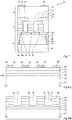
- the figure 1 represents an embodiment of an optoelectronic device 10 comprising a light-emitting diode.
- the device 10 comprises a first integrated circuit chip 11, a second integrated circuit chip 12 fixed to a first face 13 of the chip 11 and a cover 14 fixed to a second face 15 of the chip 11, opposite to the first face 13
- the device 10 is adapted to emit electromagnetic radiation from the optoelectronic chip 11 through the cover 14, that is to say downwards. figure 1 .
- the first integrated circuit chip 11 comprises at least one light emitting diode 16 and is called optoelectronic circuit or optoelectronic chip in the following description.
- the optoelectronic device shown comprises only one light-emitting diode 16.
- the second integrated circuit chip 12 provides the connection between the optoelectronic chip 11 and a support, not shown, of the device disposed on the side of the second integrated circuit chip 12 opposite to that on which the optoelectronic chip 11 is mounted.
- the second integrated circuit chip 12 may comprise electronic components, not shown, in particular transistors, used for the control or protection of the light-emitting diode 16 of the first circuit chip integrated 11.
- the second integrated circuit chip 12 is called interposer or control chip in the following description.
- the optoelectronic chip 11 is fixed to the interposer 12. Depending on the type of fixing, inserts may possibly be present between the optoelectronic chip 11 and the interposer 12.
- the thickness of the optoelectronic chip 11 is between 100 nm and 50 ⁇ m, preferably between 1 ⁇ m and 30 ⁇ m, by for example about 10 microns.
- the thickness of the interposer 12 is less than or equal to 150 ⁇ m, preferably between 1 ⁇ m and 150 ⁇ m, more preferably between 10 ⁇ m and 100 ⁇ m, for example about 30 ⁇ m.
- the cover 14 may comprise a transparent plate, for example a glass plate. The thickness of the cover 14, including any transparent plate, is greater than or equal to 100 microns.
- the light-emitting diode 16 comprises a stack of semiconductor layers each containing at least one III-V compound.
- the light-emitting diode 16 has the structure described in the application of EP2960940 which is considered an integral part of this description.
- the light-emitting diode 16 has the structure described in the publication titled "III-nitride micro-emitter arrays: development and applications” in the names of ZY Fan, JY Lin, and HX Jiang (Journal of Physics D: Applied Physics, Vol 41, Number 9, 094001, 2008 ).
- the light emitting diode 16 has a two-dimensional structure, also called mesa structure, insofar as it is formed by a stack of semiconductor layers substantially flat and comprises an active area which projects above the substrate following a step of etching its flanks.
- the optoelectronic chip 11 comprises a semiconductor layer 18 delimited by the face 15 and an opposite face 20.
- the light-emitting diode 16 rests on the face 20 of the layer 18.
- the layer 18 is, for example, a highly doped semiconductor layer of a first type of conductivity, for example of N-type.
- the layer 18 is, for example, a III-V compound, especially a III-N compound. Examples of III-N compounds are GaN, AlN, InN, InGaN, AlGaN or AlInGaN.
- the thickness of the layer 18 may be between 500 nm and 50 ⁇ m, preferably between 1 ⁇ m and 6 ⁇ m.
- the face 15 may comprise patterns 21 in relief that improve the extraction of light emitted by the light-emitting diode 16.
- the maximum thickness of the relief patterns 21 may be greater than 500 nm.
- the density of the patterns may be greater than 10 7 / cm 2 .
- the semiconductor layer 18 may not be present.
- the active zone 26 and the semiconductor portions 24 and 28 each mainly comprise at least one III-V compound, especially a III-N compound.
- III-N compounds are GaN, AlN, InN, InGaN, AlGaN or AlInGaN.
- Other group V elements may also be used, for example, phosphorus or arsenic.
- the elements in compound III-V can be combined with different mole fractions.
- the active zone 26 and the semiconductor portions 24 and 28 may each comprise a dopant.
- Active zone 26 may comprise a single quantum well. It may then comprise a semiconductor material different from the semiconductor material forming the semiconductor portions 24 and 28 and having a band gap smaller than that of the semiconductor portions 24 and 28.
- the active area 26 may comprise multiple quantum wells. It then comprises a stack of semiconductor layers forming an alternation of quantum wells and barrier layers.
- the thickness of the semiconductive portion 24 may be between 0.1 microns and 20 microns.
- the thickness of the portion Semiconductor 28 may be between 50 nm and 20 ⁇ m.
- the thickness of the active zone 26 may be between 10 nm and 500 nm.
- the width of the light-emitting diode 16 may be less than 30 ⁇ m, preferably 5 ⁇ m to 30 ⁇ m.
- an electrically conductive portion 30 covers the semiconductor portion 28.
- the conductive portions 30 are, for example, aluminum or silver.
- the thickness of each conductive portion 30 is, for example, between 3 nm and 400 nm.
- the optoelectronic chip 11 comprises a connection element 32 which electrically connects the conductive portion 30 to the interposer 12.
- the interposer 12 comprises a conductive portion 34 in contact with the connection element 32.
- the lateral flanks of the semiconductor portion 28, the active zone 26 and at least a portion of the semiconductive portion 24 are covered with an insulating portion 36.
- the thickness of the insulating portion 36 can be chosen so that the insulating portion 36 has an acceptable leakage current.
- the optoelectronic chip 11 comprises a connection element 37 which electrically connects the layer 18 to a conductive portion 39 of the interposer 12.
- the connection element 37 is electrically insulated from the semiconductor portion 28 and the active zone 26 by the portion
- the connection element 37 is in contact with the face 20 of the layer 18.
- the connection element 37 may, in addition, be in contact with a portion of the semiconductor portion 24.
- the connection elements 32 and 37 are electrically isolated from one another by an insulating region 38 which extends the insulating portion 36.
- the connection elements 32, 37 and the insulating region 38 delimit the face 13 of the optoelectronic chip 11.
- the cover 14 comprises at least one photoluminescent block 40 on the face 15 of the layer 18 vis-à-vis the light emitting diode 16, a single photoluminescent block 40 being represented in FIG. figure 1 .
- Photoluminescent block 40 is surrounded a frame 42 resting on the face 15 of the layer 18.
- the frame 42 may be made of an insulating material, semiconductor or conductive.
- the frame 42 is made of silicon.
- the thickness of the photoluminescent block 40 is between 50 ⁇ m and 200 ⁇ m, preferably between 75 ⁇ m and 150 ⁇ m, for example about 100 ⁇ m.
- the width of the photoluminescent block 40 is between 20 ⁇ m and 200 ⁇ m, preferably between 75 ⁇ m and 150 ⁇ m, for example about 100 ⁇ m.
- the photoluminescent block 40 may comprise a photoluminescent material, comprising, for example, a matrix in which are dispersed luminophores, for example yttrium garnet and aluminum (YAG, acronym for Yttrium Aluminum Garnet) activated by the ion trivalent cerium, also called YAG: This or YAG: This 3+ .
- YAG yttrium garnet and aluminum
- YAG Yttrium Aluminum Garnet
- the side walls of the frame 42 facing the photoluminescent block 40 are covered with a coating 44 adapted to reflect the radiation emitted by the photoluminescent blocks 40.
- the coating 44 is, for example, an aluminum film having a thickness of between 10 nm and 2 ⁇ m.
- the interposer 12 is mainly made of a material that is a good conductor of heat.
- the interposer 12 mainly comprises a semiconductor substrate.
- the interposer 12 may comprise conductive portions 46 on the opposite side to the optoelectronic chip 11 to allow the mechanical and / or electrical connection of the interposer 12 to a support, not shown.
- the interposer 12 comprises a connection element, not shown, connecting the conductive portion 34 to one of the conductive portions 46 and a connection element, not shown, connecting the conductive portion 34 to another of the Conductive portions 46.
- the interposer 12 comprises a semiconductor substrate and the connection elements comprise conductive vias, isolated from the substrate, and passing through the substrate throughout its thickness.
- the interposer 12 comprises components electronic, including transistors, to perform particular functions, for example the control of the light-emitting diode 16 or the protection of the light-emitting diode 16 against electrostatic discharges.
- the figure 2 represents another embodiment of an optoelectronic device 50 in which the connecting element 37 is replaced by conductive fingers 52, three fingers 52 being represented in FIG. figure 2 , which extend through the semiconductor portion 28, the active zone 26 and a portion of the semiconductor portion 24.
- Each finger 52 is surrounded by an insulating sheath 54 which electrically isolates it from the semiconductor portion 28 and the active zone 26. The end of each finger 52 is in contact with the semiconductive portion 24.
- the figure 3 represents another embodiment of an optoelectronic device 55 in which the connection between the optoelectronic chip 11 and the interposer 12 is made by electrically conductive balls 56.
- the gap 57 between the optoelectronic chip 11 and the interposer 12 is further filled with an electrically insulating material but good conductor of heat.
- the filler material may be graphite or diamond powder.
- the maximum thickness of the gap 57 is less than 5 ⁇ m, preferably less than 2 ⁇ m.
- the optoelectronic device comprises a single light-emitting diode.
- the optoelectronic device may include a plurality of light-emitting diodes that may be connected in series and / or in parallel.
- FIGs 4 and 5 illustrate embodiments in which the optoelectronic device comprises a plurality of light-emitting diodes 16.
- figure 4 represents an embodiment of an optoelectronic device 58 comprising three light-emitting diodes 16 connected in series, additional connecting elements 59 for connecting two adjacent LEDs 16 together.
- the figure 5 represents another embodiment of an optoelectronic device 60 comprising four light-emitting diodes 16 connected in parallel.
- the conductive portions 39 associated with each light-emitting diode 16 are not visible.
- the figure 6 represents another embodiment of an optoelectronic device 61 in which the lateral dimensions of the interposer 12 are greater than those of the optoelectronic chip 11.
- the electrical connection of the interposer 12 to another electronic device can then be performed on the face 62 of the interposer in contact with the face 13 of the optoelectronic chip 11.
- two conductive portions 63 on the face 62 are shown which can be used for electrical connection by wires.
- This embodiment advantageously makes it possible to fix the interposer on the whole of the face 64 opposite the face 62 on a radiator and thus to improve the evacuation of the heat produced by the optoelectronic chip 11 via the interposer 12.
- the figure 7 represents another embodiment of an optoelectronic device 65 in which the cover 14 comprises a transparent plate 66, for example a glass plate fixed to the frame 42, the photoluminescent block 40 being located between the optoelectronic chip 11 and the transparent plate 66
- the thickness of the cover 14 including the transparent plate 66 is greater than or equal to 100 ⁇ m, preferably greater than 200 ⁇ m, for example approximately 500 ⁇ m.
- the side walls of the frame 42, oriented towards the photoluminescent block 40 are inclined so as to improve the reflection of the light supplied by the light-emitting diodes 16 towards the outside of the optoelectronic device 65.
- FIG. 8A to 8N illustrate an embodiment of a method of manufacturing the optoelectronic device 10 shown in FIG. figure 1 in which the method of forming the light-emitting diodes corresponds to that described in FIG. request patent FR14 / 50077 which is considered an integral part of this description.
- the figure 8A represents the structure obtained after forming, on a substrate 67, a stack of semiconductor layers from which a plurality of light-emitting diodes 16 will be made, the conductive portions 30 on the stack and dielectric portions 68 on the conductive portions 30.
- the substrate 67 may correspond to a one-piece structure or correspond to a layer covering a support made of another material, for example glass or metal.
- the substrate is, for example, a semiconductor substrate, such as a substrate made of silicon, germanium, silicon carbide or a compound III-V, such as GaN or GaAs, in a compound II-VI, such as than ZnO.
- the substrate 67 is made of silicon, in particular monocrystalline silicon or polycrystalline silicon.
- the substrate 67 may be an insulating substrate, for example a sapphire substrate.
- the initial thickness of the optoelectronic chip 11 is between 200 ⁇ m and 2 mm.
- the conductive portions 30 are, for example, made by depositing a layer of electrically conductive material, for example aluminum or silver, followed by lithography and etching.
- the conductive portions 30 and the dielectric portions 68 each have a shape and dimensions, in the plane of the upper face of the semiconductor layer 72 on which they are made, substantially similar to those desired for the light-emitting diodes 16, for example a section disc-shaped.
- the Figure 8B represents the structure obtained after having etched the semiconductor layer 72, the active layers 71, and a first part of the semiconductor layer 70 in the pattern defined by the dielectric portions 67, forming, for each light-emitting diode 16, a mesa structure, for example of cylindrical shape, comprising the active zone 26 disposed between the semiconductor portions 24 and 28.
- This etching is stopped at a depth level located in the semiconductor layer 70 so that a portion of the layer 70 is kept at the bottom of each of the engraved areas of the stack.
- the etching step forms empty spaces 73 between the light-emitting diodes 16.
- the etching implemented is a dry etching, for example via a plasma based on Cl 2 or a reactive ion etching (RIE).
- the minimum distance between two light-emitting diodes is preferably greater than 15 ⁇ m, preferably greater than or equal to 20 ⁇ m.
- the Figure 8C represents the structure obtained after conformally depositing a dielectric layer 74, for example based on SiN, for example between about 3 nm and 100 nm, on the dielectric portions 68 and along the walls of the empty spaces 73, and covering so especially the sidewalls of conductive portions 30, semiconductor portions 28, active areas 26 and a portion of the semiconductor portions 24.
- a dielectric layer 74 for example based on SiN, for example between about 3 nm and 100 nm
- the figure 8D represents the structure obtained after performing anisotropic etching, for example a dry etching, so as to remove the portions of the dielectric layer 74 located at the bottom of the empty spaces 73 and the dielectric portions 68.
- the dielectric portions 36 are thus obtained .
- the figure 8E represents the structure obtained after having etched the rest of the semiconductor layer 70 at the bottom of the empty spaces 73 to the semiconductor layer 18, after having etched the dielectric portions 68.
- the figure 8F represents the structure obtained after having deposited an electrically conductive material 78 which fills the empty spaces 73 and covers the light-emitting diodes 16.
- the conductive material 78 is formed by the conformal deposition of a first titanium layer of thickness for example equal to about 10 nm, followed by a deposition of a second aluminum layer so as to completely fill the voids 73.
- the maximum thickness of the conductive material 78 between the bottom of the voids 73, the contact of the semiconductor layer 18, and the upper face of the conductive material 78 is, for example, equal to about 1 micron.
- the figure 8G represents the structure obtained after carrying out a planarization step, such as a chemical mechanical planarization (CMP), and / or an etching step, such as an RIE etching, of the electrically conductive material 78 until reaching the faces upper portions of the conductive portions 30 and dielectric portions 36.
- a planarization step such as a chemical mechanical planarization (CMP)
- CMP chemical mechanical planarization
- etching step such as an RIE etching
- the figure 8H represents the structure obtained after having formed the connection elements 32 and 37.
- the figure 8I represents the structure obtained after having fixed the interposer 12 to the optoelectronic chip 11 on the side of the connection elements 32.
- the initial thickness of the interposer 12 is greater than or equal to 100 ⁇ m, for example between 100 ⁇ m and 10 cm .
- the attachment of the interposer 12 to the optoelectronic chip 11 can be achieved by direct bonding, without the use of inserts such as microbeads connection.
- the direct bonding may comprise a direct metal-to-metal bonding of the metal zones 32 of the optoelectronic chip 11 and metal zones 34 to the interposer 12 and a dielectric-dielectric bonding of the dielectric zones on the surface of the optoelectronic chip 11 and the dielectric zones in FIG. interposer surface 12.
- the attachment of the interposer 12 to the optoelectronic chip 11 can be achieved by a thermocompression process in which the optoelectronic chip 11 is pressed against the interposer 12 with application of pressure and with
- the figure 8J represents the structure obtained after removing the substrate 67 so as to expose the face 15 of the semiconductor layer 18.
- the substrate 67 can be removed by a planarization step, such as a planarization mechanical-chemical (CMP), and / or an etching step, such as a RIE etching.
- CMP planarization mechanical-chemical
- etching step such as a RIE etching.
- the substrate 67 is made of an insulating material such as sapphire
- the substrate 67 can be removed by laser ablation.
- a step of forming patterns in relief on the face 15 may be provided.
- the thickness of the optoelectronic chip 11 may be between 100 nm and 50 ⁇ m, preferably between 1 ⁇ m and 30 ⁇ m, for example about 10 ⁇ m.
- the figure 8K illustrates a step of manufacturing the cover 14 and represents the structure obtained after having etched into a substrate 80, non-through openings 82 which are intended to be placed vis-à-vis the light-emitting diodes 16 and after covering the side walls openings 82 with the reflective coating 44, for example an aluminum film.
- the dimensions of the openings 82 correspond to the desired dimensions of the blocks 40 of semiconductor nanocrystals.
- the reflective coatings 44 may be formed by depositing a metal layer on the entire substrate 80 and anisotropic etching of the metal layer to retain the metal coating 44 only on the side walls of the openings 82.
- the manufacture of the cover 14 can be performed independently of the steps previously described.
- the initial thickness of the cover 14 may be greater than or equal to 100 ⁇ m, for example between 100 ⁇ m and 5 cm. Alternatively, the openings 82 may be through.
- the figure 8L represents the structure obtained after having formed the blocks 40 of semiconductor nanocrystals in at least some of the openings 82 and after having fixed the substrate 80 to the optoelectronic chip 11.
- the photoluminescent blocks 40 may be formed by filling certain openings 82 with a photoluminescent material.
- the photoluminescent material may comprise a matrix in which photoluminescent particles are dispersed.
- the method of forming the blocks 40 may correspond to a so-called additive process, for example by direct printing of the photoluminescent material at the desired locations, for example by ink jet printing, heliography, screen printing, flexography, spray coating (in English coating) or drop-casting.
- the matrix of the photoluminescent material may be a resin which is polymerized after the photoluminescent material has been deposited by printing.
- the polymerization of the matrix can be obtained by exposing the photoluminescent blocks 40 to electromagnetic radiation, in particular ultraviolet radiation. Fixing the substrate 80 to the optoelectronic chip 11 can be achieved by direct bonding or thermocompression.
- the filling of the openings 82 can be made in several stages. successive, at each step, the openings 82 being filled with a photoluminescent material while the other openings are obscured by resin.
- the figure 8M represents the structure obtained after a step of thinning the interposer 12 and a step of forming the conductive portions 46 on the face of the interposer 12 opposite to the optoelectronic chip 11.
- the thickness of the interposer 12 after the thinning step is less than or equal to 150 microns, preferably between 1 micron and 150 microns, more preferably between 10 microns and 100 microns, for example about 30 microns.
- the mechanical strength of the structure is then at least partially filled by the cover 14.
- the figure 8N represents the structure obtained after a step of thinning the substrate 80, from the side of the substrate 90 opposite the light emitting diodes 16 to expose the blocks 40 of semiconductor nanocrystals. Thinning can be achieved by mechanical and chemical planarization.
- the cover 14 may comprise a transparent plate, for example a glass plate. The thickness of the cover 14, including any transparent plate, is, after the thinning step, greater than or equal to 100 microns.
- the next step of the method comprises cutting the structure represented in figure 8N , for example according to the lines 84.
- the monolithic devices obtained after cutting then each have the structure represented in FIG. figure 1 .
- the photoluminescent blocks 40 are formed after the step of fixing the cover 14 to the optoelectronic chip 11 and the step of thinning the cover 14 in which the recesses 82 become through.
- the embodiments of the method of manufacturing the optoelectronic device described above have the advantage of not requiring the use of a temporary handle for handling integrated circuit chips. There is therefore no step of removing a temporary handle.
- the interposer 12 may be attached to a support for example by a connection type "Flip-Chip". The electrical connection of the interposer 11 can be implemented without the use of connection wires.
- FIGS. 9A to 9D are sectional, partial and schematic views of structures obtained at successive steps of an embodiment of a method of manufacturing the cover 14 of the optoelectronic device 65 shown in FIG. figure 7 .
- the Figure 9A is a figure similar to the figure 8K with the difference that the openings 82 have inclined flanks.
- the Figure 9B represents the structure obtained after fixing the transparent plate 66, in particular a glass plate, to the substrate 80, on the side of the openings 82, for example by a glass / silicon electrostatic bonding.
- the Figure 9C represents the structure obtained after a step of thinning the substrate 80, from the side of the substrate 90 opposite the transparent plate 66, to expose the openings 82.
- the thinning can be achieved by mechanical and chemical planarization.
- the thickness of the cover 14, comprising the transparent plate 66, is, after the thinning step, greater than or equal to 100 ⁇ m.
- the Figure 9D represents the structure obtained after the filling of the openings 82 by a photoluminescent material to form the photoluminescent blocks 40.
- the filling of the openings 82 can be achieved by several successive steps, at each step, the openings 82 being filled with a photoluminescent material while the other openings are obscured by the resin.
- the subsequent steps of the method include fixing the cover 14 to the optoelectronic chip 11, for example as previously described in connection with the figure 8L and cutting the resulting structure.
- the monolithic devices obtained after cutting then each have a cover 14 having the structure represented in FIG. figure 7 .
- each optoelectronic device comprises a single photoluminescent block 40
- the optoelectronic device may comprise a plurality of photoluminescent blocks, each photoluminescent block being, for example, opposite a light emitting diode.
- the structure represented figure 7 in which the cover 14 comprises a transparent plate 66 can be implemented with the other embodiments of the optoelectronic device 10, 50, 55, 58, 60 and 64 described in connection with the Figures 1, 2 , 3, 4 , 5 and 6 .
Landscapes
- Led Device Packages (AREA)
- Engineering & Computer Science (AREA)
- Led Devices (AREA)
- Manufacturing & Machinery (AREA)
- Microelectronics & Electronic Packaging (AREA)
Abstract
a) former une première puce de circuit intégré (11) comprenant des diodes électroluminescentes (16) ;
b) coller une deuxième puce de circuit intégré (12) à une première face (13) de la première puce ;
c) réduire l'épaisseur de la première puce du côté opposé à la première face jusqu'à former une deuxième face (15) opposée à la première face ;
d) coller à la deuxième face un capot (14) comprenant une plaquette de silicium munie d'évidements en regard des diodes électroluminescentes ;
e) réduire l'épaisseur de la deuxième puce ;
f) réduire l'épaisseur de la plaquette de silicium avant l'étape d) ou après l'étape e), chaque évidement étant rempli d'un matériau photoluminescent ; et
g) découper la structure obtenue à l'étape f) en plusieurs dispositifs optoélectroniques distincts.
Description
- La présente demande concerne un dispositif optoélectronique comprenant au moins une diode électroluminescente, notamment pour systèmes d'éclairage, et son procédé de fabrication.
- De façon générale, la fabrication d'un dispositif optoélectronique à diode électroluminescente comprend la fabrication de diodes électroluminescentes sur un substrat qui est ensuite découpé en puces individuelles. Chaque puce individuelle est alors montée sur un support. Différents éléments peuvent, en outre, être fixés à la puce individuelle ou au support pour réaliser diverses fonctions dont notamment la transformation du rayonnement électromagnétique émis par la diode électroluminescente en un rayonnement ayant le spectre souhaité, l'évacuation de la chaleur fournie par la diode électroluminescente, la commande électrique de la diode électroluminescente, la connexion électrique du dispositif optoélectronique à un système externe et la protection du dispositif vis-à-vis du milieu extérieur.
- Les divers procédés connus de fabrication, d'encapsulation et de montage de diodes électroluminescentes impliquent la mise en oeuvre de très nombreuses étapes dont certaines sont complexes, impliquant notamment des reports de puces et l'utilisation de poignées multiples.
- Un objet d'un mode de réalisation vise à pallier tout ou partie des inconvénients des dispositifs optoélectroniques à diodes électroluminescentes et de leurs procédés de fabrication décrits précédemment.
- Un autre objet d'un mode de réalisation est que la fabrication et l'encapsulation des diodes électroluminescentes soient réalisées de façon collective par un procédé qui soit particulièrement simple à mettre en oeuvre et qui assure que le montage des diodes électroluminescentes puisse se faire dans des conditions optimales de dissipation thermique.
- Ainsi, un mode de réalisation prévoit un procédé de fabrication de dispositifs optoélectroniques à diodes électroluminescentes comprenant les étapes suivantes :
- a) former une première puce de circuit intégré comprenant des diodes électroluminescentes ;
- b) coller une deuxième puce de circuit intégré à une première face de la première puce de circuit intégré ;
- c) réduire l'épaisseur de la première puce de circuit intégré du côté opposé à la première face jusqu'à former une deuxième face opposée à la première face, la première puce de circuit intégré ayant, après l'étape c), une première épaisseur comprise entre 100 nm et 50 µm ;
- d) coller, à la deuxième face, un capot comprenant une plaquette de silicium munie d'évidements en regard des diodes électroluminescentes, le capot comprenant éventuellement, en outre, une plaque transparente fixée à la plaquette de silicium ;
- e) réduire l'épaisseur de la deuxième puce de circuit intégré, la deuxième puce de circuit intégré ayant une deuxième épaisseur inférieure ou égale à 150 µm après l'étape e) ;
- f) réduire l'épaisseur de la plaquette de silicium avant l'étape d) ou après l'étape e), l'épaisseur du capot, comprenant éventuellement la plaque transparente, étant supérieure ou égale à 100 µm après l'étape f), chaque évidement étant rempli d'un matériau photoluminescent ; et
- g) découper la structure obtenue à l'étape f) en plusieurs dispositifs optoélectroniques distincts comprenant chacun au moins l'une des diodes électroluminescentes.
- Selon un mode de réalisation, les diodes électroluminescentes ont une structure mesa.
- Selon un mode de réalisation, les évidements sont remplis du matériau photoluminescent avant l'étape d).
- Selon un mode de réalisation, les évidements sont non traversants avant l'étape f), et sont traversants après l'étape f), le procédé comprenant, en outre, l'étape de remplissage de chaque évidement du matériau photoluminescent après l'étape f).
- Selon un mode de réalisation, les étapes b), c) et d) sont successives.
- Selon un mode de réalisation, l'étape a) comprend la formation des diodes électroluminescentes sur un substrat et l'étape c) comprend le retrait, partiel ou complet, du substrat.
- Selon un mode de réalisation, la deuxième puce de circuit intégré est fixée à la première puce de circuit intégré par collage direct et est reliée électriquement aux diodes électroluminescentes.
- Un mode de réalisation prévoit également un dispositif optoélectronique comprenant :
- une première puce de circuit intégré comprenant des première et deuxième faces opposées, ayant une épaisseur comprise entre 100 nm et 50 µm et comprenant au moins une diode électroluminescente ;
- un capot fixé à la première face, le capot comprenant au moins un évidement traversant délimité par un cadre en silicium et contenant un bloc d'un matériau photoluminescent, le capot comprenant, en outre, éventuellement une plaque transparente, l'épaisseur du capot, comprenant éventuellement la plaque transparente, étant supérieure ou égale à 100 µm ; et
- une deuxième puce de circuit intégré fixée à la deuxième face et ayant une épaisseur inférieure ou égale à 150 µm.
- Selon un mode de réalisation, la diode électroluminescente a une structure mesa.
- Selon un mode de réalisation, le bloc photoluminescent est entouré latéralement par une paroi réfléchissante.
- Ces caractéristiques et avantages, ainsi que d'autres, seront exposés en détail dans la description suivante de modes de réalisation particuliers faite à titre non limitatif en relation avec les figures jointes parmi lesquelles :
- les
figures 1 à 7 sont des vues avec coupe, partielles et schématiques, de modes de réalisation d'un dispositif optoélectronique ; - les
figures 8A à 8N sont des vues avec coupe, partielles et schématiques, de structures obtenues à des étapes successives d'un mode de réalisation d'un procédé de fabrication du dispositif optoélectronique représenté enfigure 1 ; et - les
figures 9A à 9D sont des vues avec coupe, partielles et schématiques, de structures obtenues à des étapes successives d'un mode de réalisation d'un procédé de fabrication du dispositif optoélectronique représenté enfigure 7 . - Par souci de clarté, de mêmes éléments ont été désignés par de mêmes références aux différentes figures et, de plus, comme cela est habituel dans la représentation des circuits intégrés, les diverses figures ne sont pas tracées à l'échelle. En outre, dans la suite de la description, les expressions "sensiblement", "environ" et "approximativement" signifient "à 10 % près". En outre, seuls les éléments utiles à la compréhension de la présente description ont été représentés et sont décrits. En particulier, les moyens de polarisation d'une diode électroluminescente d'un dispositif optoélectronique sont bien connus et ne sont pas décrits.
- Dans la suite de la description, on appelle "zone active" d'une diode électroluminescente la région de la diode électroluminescente depuis laquelle est émise la majorité du rayonnement électromagnétique fourni par la diode électroluminescente.
- La
figure 1 représente un mode de réalisation d'un dispositif optoélectronique 10 comprenant une diode électroluminescente. - Le dispositif 10 comprend une première puce de circuit intégré 11, une deuxième puce de circuit intégré 12 fixée à une première face 13 de la puce 11 et un capot 14 fixé à une deuxième face 15 de la puce 11, opposée à la première face 13. En fonctionnement, le dispositif 10 est adapté à émettre un rayonnement électromagnétique depuis la puce optoélectronique 11 au travers du capot 14, c'est-à-dire vers le bas en
figure 1 . - La première puce de circuit intégré 11 comprend au moins une diode électroluminescente 16 et est appelée circuit optoélectronique ou puce optoélectronique dans la suite de la description. En
figure 1 , le dispositif optoélectronique représenté ne comprend qu'une seule diode électroluminescente 16. La deuxième puce de circuit intégré 12 assure la connexion entre la puce optoélectronique 11 et un support, non représenté, du dispositif disposé du côté de la deuxième puce de circuit intégré 12 opposé à celui sur lequel est montée la puce optoélectronique 11. La deuxième puce de circuit intégré 12 peut comprendre des composants électroniques, non représentés, notamment des transistors, utilisés pour la commande ou la protection de la diode électroluminescente 16 de la première puce de circuit intégré 11. La deuxième puce de circuit intégré 12 est appelée interposeur ou puce de commande dans la suite de la description. La puce optoélectronique 11 est fixée à l'interposeur 12. Selon le type de fixation, des inserts peuvent être éventuellement présents entre la puce optoélectronique 11 et l'interposeur 12. - L'épaisseur de la puce optoélectronique 11 est comprise entre 100 nm et 50 µm, de préférence entre 1 µm et 30 µm, par exemple environ 10 µm. L'épaisseur de l'interposeur 12 est inférieure ou égale à 150 µm, de préférence comprise entre 1 µm et 150 µm, plus préférentiellement comprise entre 10 µm et 100 µm par exemple environ 30 µm. Le capot 14 peut comprendre une plaque transparente, par exemple une plaque de verre. L'épaisseur du capot 14, comprenant l'éventuelle plaque transparente, est supérieure ou égale à 100 µm.
- Selon un mode de réalisation, la diode électroluminescente 16 comprend un empilement de couches semiconductrices contenant chacune majoritairement au moins un composé III-V. Selon un premier exemple, la diode électroluminescente 16 a la structure décrite dans la demande de
brevet EP2960940 qui est considérée comme faisant partie intégrante de la présente description. Selon un deuxième exemple, la diode électroluminescente 16 a la structure décrite dans la publication intitulée "III-nitride micro-emitter arrays: development and applications" aux noms de Z.Y. Fan, J.Y. Lin, et H.X. Jiang (Journal of Physics D: Applied Physics, volume 41, numéro 9, pages 094001, 2008). Selon un mode de réalisation, la diode électroluminescente 16 a une structure bidimensionnelle, également appelée structure mesa, dans la mesure où elle est réalisée par un empilement de couches semiconductrices sensiblement planes et comprend une zone active qui se trouve en saillie au-dessus du substrat suite à une étape de gravure de ses flancs. - Selon un mode de réalisation, la puce optoélectronique 11 comprend une couche 18 semiconductrice délimitée par la face 15 et une face 20 opposée. La diode électroluminescente 16 repose sur la face 20 de la couche 18. La couche 18 est, par exemple, une couche semiconductrice fortement dopée d'un premier type de conductivité, par exemple de type N. La couche 18 est, par exemple, en un composé III-V, notamment un composé III-N. Des exemples de composés III-N sont GaN, AIN, InN, InGaN, AlGaN ou AlInGaN. L'épaisseur de la couche 18 peut être comprise entre 500 nm et 50 µm, de préférence entre 1 µm et 6 µm. La face 15 peut comprendre des motifs 21 en relief qui améliorent l'extraction de la lumière émise par la diode électroluminescente 16. L'épaisseur maximale des motifs en relief 21 peut être supérieure à 500 nm. La densité des motifs peut être supérieure à 107/cm2.
- La diode électroluminescente 16 comprend un empilement de portions de couches semiconductrices comportant, du bas vers le haut en
figure 1 : - une portion semiconductrice 24 dopée du premier type de conductivité, par exemple dopée de type N, au contact de la face 20 de la couche 18 ;
- une zone active 26 ; et
- une portion semiconductrice 28 dopée d'un deuxième type de conductivité opposé au premier type de conductivité, par exemple dopée de type P.
- Selon un autre mode de réalisation, la couche semiconductrice 18 peut ne pas être présente.
- Selon un mode de réalisation, la zone active 26 et les portions semiconductrices 24 et 28 comprennent chacune majoritairement au moins un composé III-V, notamment un composé III-N. Des exemples de composés III-N sont GaN, AIN, InN, InGaN, AlGaN ou AlInGaN. D'autres éléments du groupe V peuvent également être utilisés, par exemple, le phosphore ou l'arsenic. De façon générale, les éléments dans le composé III-V peuvent être combinés avec différentes fractions molaires. La zone active 26 et les portions semiconductrices 24 et 28 peuvent comprendre chacune un dopant.
- La zone active 26 peut comprendre un puits quantique unique. Elle peut alors comprendre un matériau semiconducteur différent du matériau semiconducteur formant les portions semiconductrices 24 et 28 et ayant une bande interdite inférieure à celle des portions semiconductrices 24 et 28. La zone active 26 peut comprendre des puits quantiques multiples. Elle comprend alors un empilement de couches semiconductrices formant une alternance de puits quantiques et de couches barrières.
- L'épaisseur de la portion semiconductrice 24 peut être comprise entre 0,1 µm et 20 µm. L'épaisseur de la portion semiconductrice 28 peut être comprise entre 50 nm et 20 µm. L'épaisseur de la zone active 26 peut être comprise entre 10 nm et 500 nm. La largeur de la diode électroluminescente 16 peut être inférieure à 30 µm, de préférence de 5 µm à 30 µm.
- Pour chaque diode électroluminescente 16, une portion conductrice électriquement 30 recouvre la portion semiconductrice 28. Les portions conductrices 30 sont, par exemple, en aluminium ou en argent. L'épaisseur de chaque portion conductrice 30 est, par exemple, comprise entre 3 nm et 400 nm. La puce optoélectronique 11 comprend un élément de connexion 32 qui relie électriquement la portion conductrice 30 à l'interposeur 12. L'interposeur 12 comprend une portion conductrice 34 au contact de l'élément de connexion 32.
- Les flancs latéraux de la portion semiconductrice 28, de la zone active 26 et au moins d'une partie de la portion semiconductrice 24 sont recouverts d'une portion isolante 36. L'épaisseur de la portion isolante 36 peut être choisie de façon que la portion isolante 36 présente un courant de fuite acceptable.
- La puce optoélectronique 11 comprend un élément de connexion 37 qui relie électriquement la couche 18 à une portion conductrice 39 de l'interposeur 12. L'élément de connexion 37 est isolé électriquement de la portion semiconductrice 28 et de la zone active 26 par la portion isolante 36. L'élément de connexion 37 est au contact de la face 20 de la couche 18. L'élément de connexion 37 peut, en outre, être au contact d'une partie de la portion semiconductrice 24. Les éléments de connexion 32 et 37 sont isolés électriquement l'un de l'autre par une région isolante 38 qui prolonge la portion isolante 36. Les éléments de connexion 32, 37 et la région isolante 38 délimitent la face 13 de la puce optoélectronique 11.
- Le capot 14 comprend au moins un bloc photoluminescent 40 sur la face 15 de la couche 18 en vis-à-vis de la diode électroluminescente 16, un seul bloc photoluminescent 40 étant représenté en
figure 1 . Le bloc photoluminescent 40 est entouré d'un cadre 42 reposant sur la face 15 de la couche 18. Le cadre 42 peut être réalisé en un matériau isolant, semiconducteur ou conducteur. A titre d'exemple, le cadre 42 est en silicium. L'épaisseur du bloc photoluminescent 40 est comprise entre 50 µm et 200 µm, de préférence comprise entre 75 µm et 150 µm, par exemple d'environ 100 µm. La largeur du bloc photoluminescent 40 est comprise entre 20 µm et 200 µm, de préférence entre 75 µm et 150 µm, par exemple d'environ 100 µm. Le bloc photoluminescent 40 peut comprendre un matériau photoluminescent, comprenant, par exemple, une matrice dans laquelle sont dispersés des luminophores, par exemple du grenat d'yttrium et d'aluminium (YAG, sigle anglais pour Yttrium Aluminium Garnet) activé par l'ion cérium trivalent, également appelé YAG:Ce ou YAG:Ce3+. - Selon un mode de réalisation, les parois latérales du cadre 42 orientées vers le bloc photoluminescent 40 sont recouvertes d'un revêtement 44 adapté à réfléchir le rayonnement émis par les blocs photoluminescents 40. Le revêtement 44 est, par exemple, un film d'aluminium ayant une épaisseur comprise entre 10 nm et 2 µm.
- De préférence, l'interposeur 12 est principalement en un matériau bon conducteur de la chaleur. Selon un mode de réalisation, l'interposeur 12 comprend principalement un substrat semiconducteur. L'interposeur 12 peut comprendre des portions conductrices 46 du côté opposé à la puce optoélectronique 11 pour permettre la connexion mécanique et/ou électrique de l'interposeur 12 à un support, non représenté. Selon un mode de réalisation, l'interposeur 12 comprend un élément de connexion, non représenté, reliant la portion conductrice 34 à l'une des portions conductrices 46 et un élément de connexion, non représenté, reliant la portion conductrice 34 à une autre des portions conductrices 46. Selon un mode de réalisation, l'interposeur 12 comprend un substrat semiconducteur et les éléments de connexion comprennent des vias conducteurs, isolés du substrat, et traversant le substrat sur toute son épaisseur. Selon un autre mode de réalisation, l'interposeur 12 comprend des composants électroniques, notamment des transistors, pour réaliser des fonctions particulières, par exemple la commande de la diode électroluminescente 16 ou la protection de la diode électroluminescente 16 contre les décharges électrostatiques.
- La
figure 2 représente un autre mode de réalisation d'un dispositif optoélectronique 50 dans lequel l'élément de connexion 37 est remplacé par des doigts conducteurs 52, trois doigts 52 étant représentés enfigure 2 , qui s'étendent au travers de la portion semiconductrice 28, de la zone active 26 et d'une partie de la portion semiconductrice 24. Chaque doigt 52 est entouré d'une gaine isolante 54 qui l'isole électriquement de la portion semiconductrice 28 et de la zone active 26. L'extrémité de chaque doigt 52 est au contact de la portion semiconductrice 24. - La
figure 3 représente un autre mode de réalisation d'un dispositif optoélectronique 55 dans lequel la liaison entre la puce optoélectronique 11 et l'interposeur 12 est réalisée par des billes conductrices électriquement 56. De préférence, l'interstice 57 entre la puce optoélectronique 11 et l'interposeur 12 est, en outre, remplie d'un matériau isolant électriquement mais bon conducteur de la chaleur. Le matériau de remplissage peut être du graphite ou de la poudre de diamant. De préférence, l'épaisseur maximale de l'interstice 57 est inférieure à 5 µm, de préférence inférieure à 2 µm. - Dans les modes de réalisation décrits précédemment, le dispositif optoélectronique comprend une seule diode électroluminescente. A titre de variante, le dispositif optoélectronique peut comprendre plusieurs diodes électroluminescentes qui peuvent être connectées en série et/ou en parallèle.
- Les
figures 4 et5 illustrent des modes de réalisation dans lesquels le dispositif optoélectronique comprend plusieurs diodes électroluminescentes 16. Lafigure 4 représente un mode de réalisation d'un dispositif optoélectronique 58 comprenant trois diodes électroluminescentes 16 connectées en série, des éléments de connexion supplémentaires 59 permettant de connecter entre elles deux diodes électroluminescentes 16 adjacentes. Lafigure 5 représente un autre mode de réalisation d'un dispositif optoélectronique 60 comprenant quatre diodes électroluminescentes 16 connectées en parallèle. Sur lafigure 5 , les portions conductrices 39 associées à chaque diode électroluminescente 16 ne sont pas visibles. - La
figure 6 représente un autre mode de réalisation d'un dispositif optoélectronique 61 dans lequel les dimensions latérales de l'interposeur 12 sont supérieures à celles de la puce optoélectronique 11. La connexion électrique de l'interposeur 12 à un autre dispositif électronique, par exemple selon une connexion par fils, peut alors être réalisée sur la face 62 de l'interposeur en contact avec la face 13 de la puce optoélectronique 11. Enfigure 6 , on a représenté deux portions conductrices 63 sur la face 62 qui peuvent être utilisées pour une connexion électrique par fils. Ce mode de réalisation permet, de façon avantageuse, de fixer l'interposeur sur la totalité de la face 64 opposée à la face 62 sur un radiateur et ainsi améliorer l'évacuation de la chaleur produite par la puce optoélectronique 11 par l'intermédiaire de l'interposeur 12. - La
figure 7 représente un autre mode de réalisation d'un dispositif optoélectronique 65 dans lequel le capot 14 comprend une plaque transparente 66, par exemple une plaque de verre fixée au cadre 42, le bloc photoluminescent 40 étant situé entre la puce optoélectronique 11 et la plaque transparente 66. L'épaisseur du capot 14 incluant la plaque transparente 66 est supérieure ou égale à 100 µm, de préférence supérieure à 200 µm, par exemple environ 500 µm. Enfigure 7 , les parois latérales du cadre 42, orientées vers le bloc photoluminescent 40, sont inclinées de façon à améliorer la réflexion de la lumière fournie par les diodes électroluminescentes 16 vers l'extérieur du dispositif optoélectronique 65. - Les
figures 8A à 8N illustrent un mode de réalisation d'un procédé de fabrication du dispositif optoélectronique 10 représenté enfigure 1 dans lequel le procédé de formation des diodes électroluminescentes correspond à celui décrit dans la demande debrevet FR14/50077 - La
figure 8A représente la structure obtenue après avoir formé, sur un substrat 67, un empilement de couches semiconductrices à partir duquel plusieurs diodes électroluminescentes 16 vont être réalisées, les portions conductrices 30 sur l'empilement et des portions diélectriques 68 sur les portions conductrices 30. Le substrat 67 peut correspondre à une structure monobloc ou correspondre à une couche recouvrant un support constitué d'un autre matériau, par exemple du verre ou du métal. Le substrat est, par exemple, un substrat semiconducteur, tel qu'un substrat en silicium, en germanium, en carbure de silicium, en un composé III-V, tel que du GaN ou du GaAs, en un composé II-VI, tel que du ZnO. De préférence, le substrat 67 est en silicium, notamment en silicium monocristallin ou polycristallin. Le substrat 67 peut être un substrat isolant, par exemple un substrat en saphir. L'épaisseur initiale de la puce optoélectronique 11 est comprise entre 200 µm et 2 mm. - L'empilement comporte, du bas vers le haut en
figure 8A : - une couche semiconductrice 69 dopée de type N, par exemple à base de GaN, qui comporte une première partie plus fortement dopée formant la couche semiconductrice 18, recouvrant le substrat 67, et recouverte d'une partie moins fortement dopée formant une couche semiconductrice 70 dopée N-. A titre de variante, les deux couches 18 et 70 peuvent correspondre à deux couches de matériaux différents. A titre d'exemple, la couche 18 peut être à base de GaN et la couche 70 peut être à base d'InGaN. En outre, que les deux couches 18 et 70 correspondent à deux couches de matériaux différents ou à une seule couche d'un même matériau, les niveaux de dopage des deux couches 18 et 70 peuvent être similaires ou non ;
- des couches actives 71 correspondant à un empilement alterné d'une ou de plusieurs couches émissives à puits quantique, par exemple à base d'InGaN, et de couches barrières, par exemple à base de GaN ; et
- une couche semiconductrice 72, par exemple du GaN, dopée de type P.
- Les portions conductrices 30 sont, par exemple, réalisées par un dépôt d'une couche de matériau électriquement conducteur, par exemple de l'aluminium ou de l'argent, suivi d'une lithographie et d'une gravure.
- Les portions conductrices 30 et les portions diélectriques 68 ont chacune une forme et des dimensions, dans le plan de la face supérieure de la couche semiconductrice 72 sur laquelle elles sont réalisées, sensiblement similaires à celles souhaitées pour les diodes électroluminescentes 16, par exemple une section en forme de disque.
- La
figure 8B représente la structure obtenue après avoir gravé la couche semiconductrice 72, les couches actives 71, et une première partie de la couche semiconductrice 70 selon le motif défini par les portions diélectriques 67, formant, pour chaque diode électroluminescente 16, une structure mesa, par exemple de forme cylindrique, comprenant la zone active 26 disposée entre les portions semiconductrices 24 et 28. Cette gravure est arrêtée à un niveau de profondeur situé dans la couche semiconductrice 70 de façon qu'une portion de la couche 70 soit conservée au fond de chacune des zones gravées de l'empilement. L'étape de gravure forme des espaces vides 73 entre les diodes électroluminescentes 16. La gravure mise en oeuvre est une gravure sèche, par exemple via un plasma à base de Cl2 ou une gravure ionique réactive (RIE). La distance minimale entre deux diodes électroluminescentes est, de préférence, supérieure à 15 µm, de préférence supérieure ou égale à 20 µm. - La
figure 8C représente la structure obtenue après avoir déposé de façon conforme une couche diélectrique 74, par exemple à base de SiN, par exemple comprise entre environ 3 nm et 100 nm, sur les portions diélectriques 68 et le long des parois des espaces vides 73, et recouvrant donc notamment les parois latérales des portions conductrices 30, des portions semiconductrices 28, des zones actives 26 et d'une partie des portions semiconductrices 24. - La
figure 8D représente la structure obtenue après avoir réalisé une gravure anisotrope, par exemple une gravure sèche, de façon à retirer les parties de la couche diélectrique 74 se trouvant au fond des espaces vides 73 et sur les portions diélectriques 68. Les portions diélectriques 36 sont ainsi obtenues. - La
figure 8E représente la structure obtenue après avoir gravé le reste de la couche semiconductrice 70 au fond des espaces vides 73 jusqu'à la couche semiconductrice 18, après avoir gravé les portions diélectriques 68. - La
figure 8F représente la structure obtenue après avoir déposé un matériau électriquement conducteur 78 qui remplit les espaces vides 73 et recouvre les diodes électroluminescentes 16. A titre d'exemple, le matériau conducteur 78 est formé par le dépôt conforme d'une première couche de titane d'épaisseur par exemple égale à environ 10 nm, suivi d'un dépôt d'une deuxième couche d'aluminium de façon à remplir en totalité les espaces vides 73. L'épaisseur maximale du matériau conducteur 78 entre le fond des espaces vides 73, au contact de la couche semiconductrice 18, et la face supérieure du matériau conducteur 78 est, par exemple, égale à environ 1 µm. - La
figure 8G représente la structure obtenue après avoir réalisé une étape de planarisation, telle qu'une planarisation mécano-chimique (CMP), et/ou une étape de gravure, telle qu'une gravure RIE, du matériau conducteur électriquement 78 jusqu'à atteindre les faces supérieures des portions conductrices 30 et des portions diélectriques 36. Les portions restantes du matériau conducteur disposées entre les diodes électroluminescentes 16 correspondent aux éléments de connexion 37. - La
figure 8H représente la structure obtenue après avoir formé les éléments de connexion 32 et 37. - La
figure 8I représente la structure obtenue après avoir fixé l'interposeur 12 à la puce optoélectronique 11 du côté des éléments de connexion 32. L'épaisseur initiale de l'interposeur 12 est supérieure ou égale à 100 µm, par exemple comprise entre 100 µm et 10 cm. La fixation de l'interposeur 12 à la puce optoélectronique 11 peut être réalisée par collage direct, sans utilisation d'inserts tels que des microbilles de connexion. Le collage direct peut comprendre un collage direct métal-métal des zones métalliques 32 de la puce optoélectronique 11 et des zones métalliques 34 l'interposeur 12 et un collage diélectrique-diélectrique des zones diélectriques en surface de la puce optoélectronique 11 et des zones diélectriques en surface de l'interposeur 12. La fixation de l'interposeur 12 à la puce optoélectronique 11 peut être réalisée par un procédé de thermocompression dans lequel la puce optoélectronique 11 est mise en appui contre l'interposeur 12 avec application d'une pression et avec chauffage. - La
figure 8J représente la structure obtenue après avoir retiré le substrat 67 de façon à exposer la face 15 de la couche semiconductrice 18. Lorsque le substrat 67 est en un matériau semiconducteur, le substrat 67 peut être retiré par une étape de planarisation, telle qu'une planarisation mécano-chimique (CMP), et/ou une étape de gravure, telle qu'une gravure RIE. Lorsque le substrat 67 est en un matériau isolant comme le saphir, le substrat 67 peut être retiré par ablation laser. Une étape de formation de motifs en relief sur la face 15 peut être prévue. Après l'étape d'amincissement, l'épaisseur de la puce optoélectronique 11 peut être comprise entre 100 nm et 50 µm, de préférence entre 1 µm et 30 µm, par exemple environ 10 µm. - La
figure 8K illustre une étape de fabrication du capot 14 et représente la structure obtenue après avoir gravé, dans un substrat 80, des ouvertures 82 non traversantes qui sont destinées à être placées en vis-à-vis des diodes électroluminescentes 16 et après avoir recouvert les parois latérales des ouvertures 82 avec le revêtement réfléchissant 44, par exemple un film d'aluminium. Les dimensions des ouvertures 82 correspondent aux dimensions souhaitées des blocs 40 de nanocristaux semiconducteurs. Les revêtements réfléchissants 44 peuvent être formés par le dépôt d'une couche métallique sur la totalité du substrat 80 et une gravure anisotrope de la couche métallique pour ne conserver le revêtement métallique 44 que sur les parois latérales des ouvertures 82. La fabrication du capot 14 peut être réalisée indépendamment des étapes décrites précédemment. L'épaisseur initiale du capot 14 peut être supérieure ou égale à 100 µm, par exemple comprise entre 100 µm et 5 cm. A titre de variante, les ouvertures 82 peuvent être traversantes. - La
figure 8L représente la structure obtenue après avoir formé les blocs 40 de nanocristaux semiconducteurs dans au moins certaines des ouvertures 82 et après avoir fixé le substrat 80 à la puce optoélectronique 11. Les blocs photoluminescents 40 peuvent être formés en remplissant certaines ouvertures 82 avec un matériau photoluminescent. Le matériau photoluminescent peut comprendre une matrice dans laquelle sont dispersées des particules photoluminescentes. Le procédé de formation des blocs 40 peut correspondre à un procédé dit additif, par exemple par impression directe du matériau photoluminescent aux emplacements souhaités, par exemple par impression par jet d'encre, héliographie, sérigraphie, flexographie, revêtement par pulvérisation (en anglais spray coating) ou dépôt de gouttes (en anglais drop-casting). La matrice du matériau photoluminescent peut être une résine que l'on fait polymériser après que le matériau photoluminescent a été déposé par impression. A titre d'exemple, la polymérisation de la matrice peut être obtenue en exposant les blocs photoluminescents 40 à un rayonnement électromagnétique, notamment un rayonnement ultraviolet. La fixation du substrat 80 à la puce optoélectronique 11 peut être réalisée par collage direct ou par thermocompression. - Dans le cas où le matériau photoluminescent n'est pas le même pour tous les blocs photoluminescents 40, le remplissage des ouvertures 82 peut être réalisé en plusieurs étapes successives, à chaque étape, des ouvertures 82 étant remplies avec un matériau photoluminescent alors que les autres ouvertures sont occultées par de la résine.
- La
figure 8M représente la structure obtenue après une étape d'amincissement de l'interposeur 12 et une étape de formation des portions conductrices 46 sur la face de l'interposeur 12 opposée à la puce optoélectronique 11. L'épaisseur de l'interposeur 12 après l'étape d'amincissement est inférieure ou égale à 150 µm, de préférence comprise entre 1 µm et 150 µm, plus préférentiellement comprise entre 10 µm et 100 µm par exemple environ 30 µm. La tenue mécanique de la structure est alors au moins en partie remplie par le capot 14. - La
figure 8N représente la structure obtenue après une étape d'amincissement du substrat 80, depuis le coté du substrat 90 opposé aux diodes électroluminescentes 16 jusqu'à exposer les blocs 40 de nanocristaux semiconducteurs. L'amincissement peut être réalisé par planarisation mécanique et chimique. Le capot 14 peut comprendre une plaque transparente, par exemple une plaque de verre. L'épaisseur du capot 14, comprenant l'éventuelle plaque transparente, est, après l'étape d'amincissement, supérieure ou égale à 100 µm. - L'étape suivante du procédé comprend la découpe de la structure représentée en
figure 8N , par exemple selon les lignes 84. Les dispositifs monolithiques obtenus après découpe ont alors chacun la structure représentée enfigure 1 . - Selon un autre mode de réalisation, les blocs photoluminescents 40 sont formés après l'étape de fixation du capot 14 à la puce optoélectronique 11 et l'étape d'amincissement du capot 14 dans laquelle les évidements 82 deviennent traversants.
- Les modes de réalisation du procédé de fabrication du dispositif optoélectronique décrits précédemment présentent l'avantage de ne pas nécessiter l'utilisation de poignée temporaire pour la manipulation des puces de circuit intégré. Il n'y a donc pas d'étape de retrait d'une poignée temporaire. En outre, l'interposeur 12 peut être fixé à un support par exemple par une liaison de type "Flip-Chip". La connexion électrique de l'interposeur 11 peut être mise en oeuvre sans utilisation de fils de connexion.
- Les
figures 9A à 9D sont des vues avec coupe, partielles et schématiques, de structures obtenues à des étapes successives d'un mode de réalisation d'un procédé de fabrication du capot 14 du dispositif optoélectronique 65 représenté enfigure 7 . - La
figure 9A est une figure analogue à lafigure 8K à la différence que les ouvertures 82 ont des flancs inclinés. - La
figure 9B représente la structure obtenue après avoir fixé la plaque transparente 66, notamment une plaque de verre, au substrat 80, du côté des ouvertures 82, par exemple par un collage électrostatique verre/silicium. - La
figure 9C représente la structure obtenue après une étape d'amincissement du substrat 80, depuis le coté du substrat 90 opposé à la plaque transparente 66, jusqu'à exposer les ouvertures 82. L'amincissement peut être réalisé par planarisation mécanique et chimique. L'épaisseur du capot 14, comprenant la plaque transparente 66, est, après l'étape d'amincissement, supérieure ou égale à 100 µm. - La
figure 9D représente la structure obtenue après le remplissage des ouvertures 82 par un matériau photoluminescent pour former les blocs photoluminescents 40. Dans le cas où le matériau photoluminescent n'est pas le même pour tous les blocs photoluminescents 40, le remplissage des ouvertures 82 peut être réalisé en plusieurs étapes successives, à chaque étape, des ouvertures 82 étant remplies avec un matériau photoluminescent alors que les autres ouvertures sont occultées par de la résine. - Les étapes ultérieures du procédé comprennent la fixation du capot 14 à la puce optoélectronique 11, par exemple comme cela a été décrit précédemment en relation avec la
figure 8L et la découpe de la structure obtenue. Les dispositifs monolithiques obtenus après découpe ont alors chacun un capot 14 ayant la structure représentée enfigure 7 . - Des modes de réalisation particuliers ont été décrits. Diverses variantes et modifications apparaîtront à l'homme de l'art. En particulier, bien que, dans les modes de réalisation décrits précédemment, chaque dispositif optoélectronique comprenne un seul bloc photoluminescent 40, il est clair que le dispositif optoélectronique peut comprendre plusieurs blocs photoluminescents, chaque bloc photoluminescent étant, par exemple, en regard d'une diode électroluminescente.
- Divers modes de réalisation avec diverses variantes ont été décrits ci-dessus. On note que l'homme de l'art peut combiner divers éléments de ces divers modes de réalisation et variantes sans faire preuve d'activité inventive. En particulier, la structure représentée en
figure 6 , dans laquelle la connexion électrique entre l'interposeur 12 et un autre dispositif électronique est réalisée sur la face 62 de l'interposeur 12 en contact avec la puce optoélectronique 11, peut être mise en oeuvre avec les autres modes de réalisation du dispositif optoélectronique 10, 50, 55, 58, 60 et 65 décrits en relation avec lesfigures 1, 2 ,3, 4 ,5 et7 . En outre, la structure représentée enfigure 7 dans laquelle le capot 14 comprend une plaque transparente 66 peut être mise en oeuvre avec les autres modes de réalisation du dispositif optoélectronique 10, 50, 55, 58, 60 et 64 décrits en relation avec lesfigures 1, 2 ,3, 4 ,5 et 6 .
Claims (10)
- Procédé de fabrication de dispositifs optoélectroniques (10 ; 50 ; 55 ; 58 ; 59) à diodes électroluminescentes comprenant les étapes suivantes :a) former une première puce de circuit intégré (11) comprenant des diodes électroluminescentes (16) ;b) coller une deuxième puce de circuit intégré (12) à une première face (13) de la première puce de circuit intégré ;c) réduire l'épaisseur de la première puce de circuit intégré du côté opposé à la première face jusqu'à former une deuxième face (15) opposée à la première face, la première puce de circuit intégré ayant, après l'étape c), une première épaisseur comprise entre 100 nm et 50 µm ;d) coller, à la deuxième face, un capot (14) comprenant une plaquette de silicium (80) munie d'évidements (82) en regard des diodes électroluminescentes, le capot comprenant éventuellement, en outre, une plaque transparente (66) fixée à la plaquette de silicium ;e) réduire l'épaisseur de la deuxième puce de circuit intégré, la deuxième puce de circuit intégré ayant une deuxième épaisseur inférieure ou égale à 150 µm après l'étape e) ;f) réduire l'épaisseur de la plaquette de silicium (80) avant l'étape d) ou après l'étape e), l'épaisseur du capot, comprenant éventuellement la plaque transparente, étant supérieure ou égale à 100 µm après l'étape f), chaque évidement étant rempli d'un matériau photoluminescent ; etg) découper la structure obtenue à l'étape f) en plusieurs dispositifs optoélectroniques distincts comprenant chacun au moins l'une des diodes électroluminescentes.
- Procédé selon la revendication 1, dans lequel les diodes électroluminescentes (16) ont une structure mesa.
- Procédé selon la revendication 1 ou 2, dans lequel les évidements (82) sont remplis du matériau photoluminescent avant l'étape d).
- Procédé selon la revendication 1 ou 2, dans lequel les évidements (82) sont non traversants avant l'étape f), et sont traversants après l'étape f), le procédé comprenant, en outre, l'étape de remplissage de chaque évidement du matériau photoluminescent après l'étape f).
- Procédé selon l'une quelconque des revendications 1 à 4, dans lequel les étapes b), c) et d) sont successives.
- Procédé selon l'une quelconque des revendications 1 à 5, dans lequel l'étape a) comprend la formation des diodes électroluminescentes (16) sur un substrat (67) et l'étape c) comprend le retrait, partiel ou complet, du substrat.
- Procédé selon l'une quelconque des revendications 1 à 6, dans lequel la deuxième puce de circuit intégré (12) est fixée à la première puce de circuit intégré (11) par collage direct et est reliée électriquement aux diodes électroluminescentes (16).
- Dispositif optoélectronique (10 ; 50 ; 55 ; 58 ; 59) comprenant :une première puce de circuit intégré (11) comprenant des première et deuxième faces (13, 15) opposées, ayant une épaisseur comprise entre 100 nm et 50 µm et comprenant au moins une diode électroluminescente (16) ;un capot (14) fixé à la première face, le capot comprenant au moins un évidement traversant (82) délimité par un cadre (42) en silicium et contenant un bloc (40) d'un matériau photoluminescent, le capot comprenant, en outre, éventuellement une plaque transparente (66), l'épaisseur du capot, comprenant éventuellement la plaque transparente, étant supérieure ou égale à 100 µm ; etune deuxième puce de circuit intégré (12) fixée à la deuxième face et ayant une épaisseur inférieure ou égale à 150 µm.
- Dispositif optoélectronique selon la revendication 8, dans lequel la diode électroluminescente (16) a une structure mesa.
- Dispositif optoélectronique selon la revendication 8 ou 9, dans lequel le bloc photoluminescent (40) est entouré latéralement par une paroi réfléchissante (44).
Applications Claiming Priority (1)
| Application Number | Priority Date | Filing Date | Title |
|---|---|---|---|
| FR1552348A FR3033939B1 (fr) | 2015-03-20 | 2015-03-20 | Dispositif optoelectronique a diode electroluminescente |
Publications (2)
| Publication Number | Publication Date |
|---|---|
| EP3070752A1 true EP3070752A1 (fr) | 2016-09-21 |
| EP3070752B1 EP3070752B1 (fr) | 2019-04-10 |
Family
ID=53674056
Family Applications (1)
| Application Number | Title | Priority Date | Filing Date |
|---|---|---|---|
| EP16160762.7A Active EP3070752B1 (fr) | 2015-03-20 | 2016-03-16 | Procédé de fabrication de dispositif optoélectronique à diode électroluminescente |
Country Status (5)
| Country | Link |
|---|---|
| US (1) | US9735139B2 (fr) |
| EP (1) | EP3070752B1 (fr) |
| JP (1) | JP2016178307A (fr) |
| KR (1) | KR20160113042A (fr) |
| FR (1) | FR3033939B1 (fr) |
Cited By (7)
| Publication number | Priority date | Publication date | Assignee | Title |
|---|---|---|---|---|
| WO2018122354A1 (fr) * | 2016-12-29 | 2018-07-05 | Aledia | Dispositif optoélectronique à diodes électroluminescentes |
| WO2019239059A1 (fr) * | 2018-06-14 | 2019-12-19 | Aledia | Dispositif optoélectronique |
| EP3624192A1 (fr) * | 2018-09-13 | 2020-03-18 | Commissariat à l'Energie Atomique et aux Energies Alternatives | Procédé de fabrication d'un dispositif optoélectronique comprenant une pluralité de diodes |
| FR3102298A1 (fr) * | 2019-10-16 | 2021-04-23 | Aledia | Procede de protection d'un dispositif optoelectronique contre les decharges electrostatiques |
| FR3102613A1 (fr) * | 2019-10-28 | 2021-04-30 | Commissariat A L'energie Atomique Et Aux Energies Alternatives | Procede de realisation d’une diode photo-emettrice ou photo-receptrice |
| CN113808988A (zh) * | 2020-06-16 | 2021-12-17 | 台湾爱司帝科技股份有限公司 | 发光芯片承载结构及其制作方法 |
| FR3114685A1 (fr) * | 2020-09-30 | 2022-04-01 | Aledia | Dispositif optoélectronique |
Families Citing this family (23)
| Publication number | Priority date | Publication date | Assignee | Title |
|---|---|---|---|---|
| US10177127B2 (en) | 2015-09-04 | 2019-01-08 | Hong Kong Beida Jade Bird Display Limited | Semiconductor apparatus and method of manufacturing the same |
| US10304811B2 (en) | 2015-09-04 | 2019-05-28 | Hong Kong Beida Jade Bird Display Limited | Light-emitting diode display panel with micro lens array |
| US10032757B2 (en) | 2015-09-04 | 2018-07-24 | Hong Kong Beida Jade Bird Display Limited | Projection display system |
| FR3061358B1 (fr) * | 2016-12-27 | 2021-06-11 | Aledia | Procede de fabrication d’un dispositif optoelectronique comportant des plots photoluminescents de photoresine |
| US12322732B2 (en) | 2017-02-09 | 2025-06-03 | Vuereal Inc. | Circuit and system integration onto a microdevice substrate |
| US11916096B2 (en) * | 2017-02-09 | 2024-02-27 | Vuereal Inc. | Circuit and system integration onto a micro-device substrate |
| FR3066320B1 (fr) * | 2017-05-11 | 2019-07-12 | Commissariat A L'energie Atomique Et Aux Energies Alternatives | Procede de fabrication d'un dispositif d'affichage emissif a led |
| CN107611232B (zh) * | 2017-08-21 | 2019-02-05 | 天津三安光电有限公司 | 发光二极管及其制作方法 |
| FR3073669B1 (fr) * | 2017-11-10 | 2021-11-05 | Commissariat Energie Atomique | Procede de fabrication d'un dispositif optoelectronique comprenant une pluralite de diodes |
| FR3076170B1 (fr) * | 2017-12-22 | 2020-05-15 | Commissariat A L'energie Atomique Et Aux Energies Alternatives | Procede de report de structures electroluminescentes |
| CN119497483A (zh) | 2018-01-24 | 2025-02-21 | 苹果公司 | 基于微型led的显示面板 |
| FR3083045B1 (fr) * | 2018-06-26 | 2020-07-31 | Aledia | Dispositif optoelectronique a diodes electroluminescentes |
| US11056611B2 (en) * | 2018-09-11 | 2021-07-06 | Facebook Technologies, Llc | Mesa formation for wafer-to-wafer bonding |
| US11145786B2 (en) | 2018-09-11 | 2021-10-12 | Facebook Technologies, Llc | Methods for wafer-to-wafer bonding |
| US11342479B2 (en) | 2018-09-11 | 2022-05-24 | Facebook Technologies, Llc | Reducing bowing of materials before wafer-to-wafer bonding for LED manufacturing |
| JP6915029B2 (ja) | 2018-11-30 | 2021-08-04 | シャープ株式会社 | マイクロ発光素子及び画像表示素子 |
| JP7270131B2 (ja) * | 2019-03-28 | 2023-05-10 | 日亜化学工業株式会社 | 発光装置の製造方法 |
| GB2595252B (en) * | 2020-05-19 | 2023-10-11 | Plessey Semiconductors Ltd | Monolithic RGB micro LED display |
| EP4162481A4 (fr) * | 2020-06-03 | 2024-10-16 | Jade Bird Display (Shanghai) Limited | Systèmes et procédés pour unité de pixel à del multicolore avec émission de lumière verticale |
| EP3923424B1 (fr) * | 2020-06-09 | 2024-07-24 | Imec VZW | Procédé de traitement d'un dispositif laser |
| GB2596533B (en) * | 2020-06-29 | 2023-02-15 | Plessey Semiconductors Ltd | Hybrid microdisplay |
| CN114335060B (zh) * | 2021-12-24 | 2025-06-24 | 季华实验室 | 防串扰微显示阵列 |
| DE102022119365A1 (de) * | 2022-08-02 | 2024-02-08 | Ams-Osram International Gmbh | Herstellung einer leuchtvorrichtung |
Citations (5)
| Publication number | Priority date | Publication date | Assignee | Title |
|---|---|---|---|---|
| FR1450077A (fr) | 1965-10-08 | 1966-05-06 | Burgue Freres Ets | étoffe pour la réalisation d'articles vestimentaires, et articles vestimentaires réalisés à partir de cette étoffe |
| US20100244065A1 (en) * | 2009-03-30 | 2010-09-30 | Koninklijke Philips Electronics N.V. | Semiconductor light emitting device grown on an etchable substrate |
| WO2011108664A1 (fr) * | 2010-03-03 | 2011-09-09 | 有限会社Mtec | Dispositif optique à semi-conducteur |
| WO2012164437A2 (fr) * | 2011-06-01 | 2012-12-06 | Koninklijke Philips Electronics N.V. | Dispositif émetteur de lumière lié à un substrat de support |
| EP2960940A1 (fr) | 2014-06-27 | 2015-12-30 | Commissariat à l'Énergie Atomique et aux Énergies Alternatives | Diode de structure mesa a surface de contact sensiblement plane |
Family Cites Families (15)
| Publication number | Priority date | Publication date | Assignee | Title |
|---|---|---|---|---|
| JP3728147B2 (ja) * | 1999-07-16 | 2005-12-21 | キヤノン株式会社 | 光電気混載配線基板 |
| JP3975194B2 (ja) * | 2003-12-02 | 2007-09-12 | 株式会社フジクラ | パッケージの製造方法 |
| DE102005019375A1 (de) * | 2005-02-28 | 2006-09-07 | Osram Opto Semiconductors Gmbh | LED-Array |
| US20110049545A1 (en) * | 2009-09-02 | 2011-03-03 | Koninklijke Philips Electronics N.V. | Led package with phosphor plate and reflective substrate |
| US8198109B2 (en) * | 2010-08-27 | 2012-06-12 | Quarkstar Llc | Manufacturing methods for solid state light sheet or strip with LEDs connected in series for general illumination |
| CN107706279B (zh) * | 2011-06-01 | 2020-10-30 | 亮锐控股有限公司 | 发光器件以及将发光器件附着到支撑衬底的方法 |
| US8796665B2 (en) * | 2011-08-26 | 2014-08-05 | Micron Technology, Inc. | Solid state radiation transducers and methods of manufacturing |
| DE102011056888A1 (de) * | 2011-12-22 | 2013-06-27 | Osram Opto Semiconductors Gmbh | Anzeigevorrichtung und Verfahren zur Herstellung einer Anzeigevorrichtung |
| CN202523750U (zh) * | 2011-12-31 | 2012-11-07 | 刘胜 | Led圆片级芯片尺寸封装结构 |
| WO2013116623A1 (fr) * | 2012-02-02 | 2013-08-08 | The Procter & Gamble Company | Feuille de lumière bidirectionnelle |
| EP2875532B1 (fr) * | 2012-07-20 | 2019-02-27 | Lumileds Holding B.V. | Led à phosphore vert en céramique et couche de phosphore rouge protégée |
| DE102012109460B4 (de) * | 2012-10-04 | 2024-03-07 | OSRAM Opto Semiconductors Gesellschaft mit beschränkter Haftung | Verfahren zur Herstellung eines Leuchtdioden-Displays und Leuchtdioden-Display |
| FR3003403B1 (fr) * | 2013-03-14 | 2016-11-04 | Commissariat Energie Atomique | Procede de formation de diodes electroluminescentes |
| WO2015004577A1 (fr) * | 2013-07-08 | 2015-01-15 | Koninklijke Philips N.V. | Dispositif électroluminescent à semi-conducteur à conversion de longueur d'onde |
| TWI509842B (zh) * | 2013-09-02 | 2015-11-21 | Lextar Electronics Corp | 發光二極體的封裝結構及其製造方法 |
-
2015
- 2015-03-20 FR FR1552348A patent/FR3033939B1/fr not_active Expired - Fee Related
-
2016
- 2016-03-16 EP EP16160762.7A patent/EP3070752B1/fr active Active
- 2016-03-18 KR KR1020160032747A patent/KR20160113042A/ko not_active Withdrawn
- 2016-03-18 US US15/074,980 patent/US9735139B2/en not_active Expired - Fee Related
- 2016-03-22 JP JP2016057295A patent/JP2016178307A/ja active Pending
Patent Citations (5)
| Publication number | Priority date | Publication date | Assignee | Title |
|---|---|---|---|---|
| FR1450077A (fr) | 1965-10-08 | 1966-05-06 | Burgue Freres Ets | étoffe pour la réalisation d'articles vestimentaires, et articles vestimentaires réalisés à partir de cette étoffe |
| US20100244065A1 (en) * | 2009-03-30 | 2010-09-30 | Koninklijke Philips Electronics N.V. | Semiconductor light emitting device grown on an etchable substrate |
| WO2011108664A1 (fr) * | 2010-03-03 | 2011-09-09 | 有限会社Mtec | Dispositif optique à semi-conducteur |
| WO2012164437A2 (fr) * | 2011-06-01 | 2012-12-06 | Koninklijke Philips Electronics N.V. | Dispositif émetteur de lumière lié à un substrat de support |
| EP2960940A1 (fr) | 2014-06-27 | 2015-12-30 | Commissariat à l'Énergie Atomique et aux Énergies Alternatives | Diode de structure mesa a surface de contact sensiblement plane |
Non-Patent Citations (1)
| Title |
|---|
| Z.Y. FAN; J.Y. LIN; H.X. JIANG: "III-nitride micro-emitter arrays: development and applications", JOURNAL OF PHYSICS D: APPLIED PHYSICS, vol. 41, no. 9, 2008, pages 094001, XP020133616 |
Cited By (16)
| Publication number | Priority date | Publication date | Assignee | Title |
|---|---|---|---|---|
| FR3061603A1 (fr) * | 2016-12-29 | 2018-07-06 | Aledia | Dispositif optoelectronique a diodes electroluminescentes |
| US10916580B2 (en) | 2016-12-29 | 2021-02-09 | Aledia | Optoelectronic device with light-emitting diodes |
| WO2018122354A1 (fr) * | 2016-12-29 | 2018-07-05 | Aledia | Dispositif optoélectronique à diodes électroluminescentes |
| WO2019239059A1 (fr) * | 2018-06-14 | 2019-12-19 | Aledia | Dispositif optoélectronique |
| FR3082663A1 (fr) * | 2018-06-14 | 2019-12-20 | Aledia | Dispositif optoelectronique |
| US11581295B2 (en) | 2018-06-14 | 2023-02-14 | Aledia | Optoelectronic device |
| US11444118B2 (en) | 2018-09-13 | 2022-09-13 | Commissariat à l'énergie atomique et aux énergies alternatives | Method of manufacturing an optoelectronic device comprising a plurality of diodes |
| EP3624192A1 (fr) * | 2018-09-13 | 2020-03-18 | Commissariat à l'Energie Atomique et aux Energies Alternatives | Procédé de fabrication d'un dispositif optoélectronique comprenant une pluralité de diodes |
| FR3086100A1 (fr) * | 2018-09-13 | 2020-03-20 | Commissariat A L'energie Atomique Et Aux Energies Alternatives | Procede de fabrication d'un dispositif optoelectronique comprenant une pluralite de diodes |
| FR3102298A1 (fr) * | 2019-10-16 | 2021-04-23 | Aledia | Procede de protection d'un dispositif optoelectronique contre les decharges electrostatiques |
| FR3102613A1 (fr) * | 2019-10-28 | 2021-04-30 | Commissariat A L'energie Atomique Et Aux Energies Alternatives | Procede de realisation d’une diode photo-emettrice ou photo-receptrice |
| EP3817054A1 (fr) * | 2019-10-28 | 2021-05-05 | Commissariat à l'énergie atomique et aux énergies alternatives | Procédé de réalisation d'une diode photo-émettrice ou photo-réceptrice |
| CN113808988A (zh) * | 2020-06-16 | 2021-12-17 | 台湾爱司帝科技股份有限公司 | 发光芯片承载结构及其制作方法 |
| CN113808988B (zh) * | 2020-06-16 | 2024-06-07 | 台湾爱司帝科技股份有限公司 | 发光芯片承载结构及其制作方法 |
| FR3114685A1 (fr) * | 2020-09-30 | 2022-04-01 | Aledia | Dispositif optoélectronique |
| WO2022069506A1 (fr) * | 2020-09-30 | 2022-04-07 | Aledia | Dispositif optoelectronique |
Also Published As
| Publication number | Publication date |
|---|---|
| JP2016178307A (ja) | 2016-10-06 |
| US20160276329A1 (en) | 2016-09-22 |
| KR20160113042A (ko) | 2016-09-28 |
| FR3033939A1 (fr) | 2016-09-23 |
| FR3033939B1 (fr) | 2018-04-27 |
| US9735139B2 (en) | 2017-08-15 |
| EP3070752B1 (fr) | 2019-04-10 |
Similar Documents
| Publication | Publication Date | Title |
|---|---|---|
| EP3070752B1 (fr) | Procédé de fabrication de dispositif optoélectronique à diode électroluminescente | |
| EP3782193B1 (fr) | Procédé de fabrication d'un dispositif optoélectronique à matrice de diodes | |
| EP3024030B1 (fr) | Dispositif optoélectronique à diodes électroluminescentes et son procédé de fabrication | |
| EP2973750B1 (fr) | Procede de formation de diodes electroluminescentes | |
| FR3023065A1 (fr) | Dispositif optoelectronique a jonction p-n permettant une ionisation de dopants par effet de champ | |
| KR102743118B1 (ko) | 발광 다이오드 및 발광 다이오드 어레이 | |
| FR3091022A1 (fr) | Procede de fabrication de structures optoelectroniques pourvues de diodes electroluminescentes coplanaires | |
| FR3061608A1 (fr) | Dispositif optoelectronique a diodes electroluminescentes | |
| EP3732725B1 (fr) | Dispositif optoélectronique à matrice de diodes tridimensionnelles | |
| FR3068516A1 (fr) | Dispositif optoelectronique comprenant des diodes electroluminescentes | |
| FR3061605A1 (fr) | Dispositif optoélectronique à diodes électroluminescentes | |
| CN101617415B (zh) | 制造薄膜半导体结构的方法 | |
| KR20220160652A (ko) | 모놀리식 led 픽셀 | |
| TWI796658B (zh) | 單體電子器件、測試基片及其形成與測試方法 | |
| WO2015155437A1 (fr) | Dispositif optoelectronique a diodes electroluminescentes et a diagramme d'emission ameliore | |
| EP3394882A1 (fr) | Circuit electronique comprenant des tranchees d'isolation electrique | |
| EP3549178B1 (fr) | Dispositif optoélectronique à diode électroluminescente à extraction augmentée | |
| FR3137242A1 (fr) | Dispositif optoélectronique et procédé de fabrication | |
| US11404471B2 (en) | Optoelectronic semiconductor component, and method for producing an optoelectronic semiconductor component | |
| WO2024141240A1 (fr) | Procede de fabrication d'un dispositif electronique | |
| US20210126155A1 (en) | Method for Producing a Component and Optoelectronic Component | |
| EP4576182A2 (fr) | Procédé de fabrication d'un dispositif électronique | |
| FR3082661A1 (fr) | Dispositif optoelectronique a diodes electroluminescentes | |
| CN104704642B (zh) | 用于制造光电子器件的方法 | |
| FR3075464A1 (fr) | Dispositif optoelectronique a diodes electroluminescentes |
Legal Events
| Date | Code | Title | Description |
|---|---|---|---|
| PUAI | Public reference made under article 153(3) epc to a published international application that has entered the european phase |
Free format text: ORIGINAL CODE: 0009012 |
|
| AK | Designated contracting states |
Kind code of ref document: A1 Designated state(s): AL AT BE BG CH CY CZ DE DK EE ES FI FR GB GR HR HU IE IS IT LI LT LU LV MC MK MT NL NO PL PT RO RS SE SI SK SM TR |
|
| AX | Request for extension of the european patent |
Extension state: BA ME |
|
| STAA | Information on the status of an ep patent application or granted ep patent |
Free format text: STATUS: REQUEST FOR EXAMINATION WAS MADE |
|
| 17P | Request for examination filed |
Effective date: 20170316 |
|
| RBV | Designated contracting states (corrected) |
Designated state(s): AL AT BE BG CH CY CZ DE DK EE ES FI FR GB GR HR HU IE IS IT LI LT LU LV MC MK MT NL NO PL PT RO RS SE SI SK SM TR |
|
| REG | Reference to a national code |
Ref country code: DE Ref legal event code: R079 Ref document number: 602016012085 Country of ref document: DE Free format text: PREVIOUS MAIN CLASS: H01L0033480000 Ipc: H01L0033000000 |
|
| GRAP | Despatch of communication of intention to grant a patent |
Free format text: ORIGINAL CODE: EPIDOSNIGR1 |
|
| STAA | Information on the status of an ep patent application or granted ep patent |
Free format text: STATUS: GRANT OF PATENT IS INTENDED |
|
| RIC1 | Information provided on ipc code assigned before grant |
Ipc: H01L 33/62 20100101ALI20181213BHEP Ipc: H01L 33/60 20100101ALI20181213BHEP Ipc: H01L 33/50 20100101ALI20181213BHEP Ipc: H01L 33/20 20100101ALN20181213BHEP Ipc: H01L 27/15 20060101ALI20181213BHEP Ipc: H01L 33/00 20100101AFI20181213BHEP Ipc: H01L 33/64 20100101ALN20181213BHEP |
|
| RIC1 | Information provided on ipc code assigned before grant |
Ipc: H01L 33/64 20100101ALN20181220BHEP Ipc: H01L 27/15 20060101ALI20181220BHEP Ipc: H01L 33/22 20100101ALN20181220BHEP Ipc: H01L 33/38 20100101ALN20181220BHEP Ipc: H01L 33/08 20100101ALN20181220BHEP Ipc: H01L 33/60 20100101ALI20181220BHEP Ipc: H01L 33/62 20100101ALI20181220BHEP Ipc: H01L 33/20 20100101ALN20181220BHEP Ipc: H01L 33/50 20100101ALI20181220BHEP Ipc: H01L 33/00 20100101AFI20181220BHEP |
|
| INTG | Intention to grant announced |
Effective date: 20190110 |
|
| GRAS | Grant fee paid |
Free format text: ORIGINAL CODE: EPIDOSNIGR3 |
|
| GRAA | (expected) grant |
Free format text: ORIGINAL CODE: 0009210 |
|
| STAA | Information on the status of an ep patent application or granted ep patent |
Free format text: STATUS: THE PATENT HAS BEEN GRANTED |
|
| AK | Designated contracting states |
Kind code of ref document: B1 Designated state(s): AL AT BE BG CH CY CZ DE DK EE ES FI FR GB GR HR HU IE IS IT LI LT LU LV MC MK MT NL NO PL PT RO RS SE SI SK SM TR |
|
| REG | Reference to a national code |
Ref country code: GB Ref legal event code: FG4D Free format text: NOT ENGLISH |
|
| REG | Reference to a national code |
Ref country code: CH Ref legal event code: EP Ref country code: AT Ref legal event code: REF Ref document number: 1119866 Country of ref document: AT Kind code of ref document: T Effective date: 20190415 |
|
| REG | Reference to a national code |
Ref country code: IE Ref legal event code: FG4D Free format text: LANGUAGE OF EP DOCUMENT: FRENCH |
|
| REG | Reference to a national code |
Ref country code: DE Ref legal event code: R096 Ref document number: 602016012085 Country of ref document: DE |
|
| REG | Reference to a national code |
Ref country code: NL Ref legal event code: MP Effective date: 20190410 |
|
| REG | Reference to a national code |
Ref country code: LT Ref legal event code: MG4D |
|
| REG | Reference to a national code |
Ref country code: AT Ref legal event code: MK05 Ref document number: 1119866 Country of ref document: AT Kind code of ref document: T Effective date: 20190410 |
|
| PG25 | Lapsed in a contracting state [announced via postgrant information from national office to epo] |
Ref country code: NL Free format text: LAPSE BECAUSE OF FAILURE TO SUBMIT A TRANSLATION OF THE DESCRIPTION OR TO PAY THE FEE WITHIN THE PRESCRIBED TIME-LIMIT Effective date: 20190410 |
|
| PG25 | Lapsed in a contracting state [announced via postgrant information from national office to epo] |
Ref country code: FI Free format text: LAPSE BECAUSE OF FAILURE TO SUBMIT A TRANSLATION OF THE DESCRIPTION OR TO PAY THE FEE WITHIN THE PRESCRIBED TIME-LIMIT Effective date: 20190410 Ref country code: SE Free format text: LAPSE BECAUSE OF FAILURE TO SUBMIT A TRANSLATION OF THE DESCRIPTION OR TO PAY THE FEE WITHIN THE PRESCRIBED TIME-LIMIT Effective date: 20190410 Ref country code: LT Free format text: LAPSE BECAUSE OF FAILURE TO SUBMIT A TRANSLATION OF THE DESCRIPTION OR TO PAY THE FEE WITHIN THE PRESCRIBED TIME-LIMIT Effective date: 20190410 Ref country code: AL Free format text: LAPSE BECAUSE OF FAILURE TO SUBMIT A TRANSLATION OF THE DESCRIPTION OR TO PAY THE FEE WITHIN THE PRESCRIBED TIME-LIMIT Effective date: 20190410 Ref country code: NO Free format text: LAPSE BECAUSE OF FAILURE TO SUBMIT A TRANSLATION OF THE DESCRIPTION OR TO PAY THE FEE WITHIN THE PRESCRIBED TIME-LIMIT Effective date: 20190710 Ref country code: ES Free format text: LAPSE BECAUSE OF FAILURE TO SUBMIT A TRANSLATION OF THE DESCRIPTION OR TO PAY THE FEE WITHIN THE PRESCRIBED TIME-LIMIT Effective date: 20190410 Ref country code: PT Free format text: LAPSE BECAUSE OF FAILURE TO SUBMIT A TRANSLATION OF THE DESCRIPTION OR TO PAY THE FEE WITHIN THE PRESCRIBED TIME-LIMIT Effective date: 20190910 Ref country code: HR Free format text: LAPSE BECAUSE OF FAILURE TO SUBMIT A TRANSLATION OF THE DESCRIPTION OR TO PAY THE FEE WITHIN THE PRESCRIBED TIME-LIMIT Effective date: 20190410 |
|
| PG25 | Lapsed in a contracting state [announced via postgrant information from national office to epo] |
Ref country code: GR Free format text: LAPSE BECAUSE OF FAILURE TO SUBMIT A TRANSLATION OF THE DESCRIPTION OR TO PAY THE FEE WITHIN THE PRESCRIBED TIME-LIMIT Effective date: 20190711 Ref country code: BG Free format text: LAPSE BECAUSE OF FAILURE TO SUBMIT A TRANSLATION OF THE DESCRIPTION OR TO PAY THE FEE WITHIN THE PRESCRIBED TIME-LIMIT Effective date: 20190710 Ref country code: PL Free format text: LAPSE BECAUSE OF FAILURE TO SUBMIT A TRANSLATION OF THE DESCRIPTION OR TO PAY THE FEE WITHIN THE PRESCRIBED TIME-LIMIT Effective date: 20190410 Ref country code: RS Free format text: LAPSE BECAUSE OF FAILURE TO SUBMIT A TRANSLATION OF THE DESCRIPTION OR TO PAY THE FEE WITHIN THE PRESCRIBED TIME-LIMIT Effective date: 20190410 Ref country code: LV Free format text: LAPSE BECAUSE OF FAILURE TO SUBMIT A TRANSLATION OF THE DESCRIPTION OR TO PAY THE FEE WITHIN THE PRESCRIBED TIME-LIMIT Effective date: 20190410 |
|
| PG25 | Lapsed in a contracting state [announced via postgrant information from national office to epo] |
Ref country code: AT Free format text: LAPSE BECAUSE OF FAILURE TO SUBMIT A TRANSLATION OF THE DESCRIPTION OR TO PAY THE FEE WITHIN THE PRESCRIBED TIME-LIMIT Effective date: 20190410 Ref country code: IS Free format text: LAPSE BECAUSE OF FAILURE TO SUBMIT A TRANSLATION OF THE DESCRIPTION OR TO PAY THE FEE WITHIN THE PRESCRIBED TIME-LIMIT Effective date: 20190810 |
|
| REG | Reference to a national code |
Ref country code: DE Ref legal event code: R097 Ref document number: 602016012085 Country of ref document: DE |
|
| PG25 | Lapsed in a contracting state [announced via postgrant information from national office to epo] |
Ref country code: CZ Free format text: LAPSE BECAUSE OF FAILURE TO SUBMIT A TRANSLATION OF THE DESCRIPTION OR TO PAY THE FEE WITHIN THE PRESCRIBED TIME-LIMIT Effective date: 20190410 Ref country code: RO Free format text: LAPSE BECAUSE OF FAILURE TO SUBMIT A TRANSLATION OF THE DESCRIPTION OR TO PAY THE FEE WITHIN THE PRESCRIBED TIME-LIMIT Effective date: 20190410 Ref country code: EE Free format text: LAPSE BECAUSE OF FAILURE TO SUBMIT A TRANSLATION OF THE DESCRIPTION OR TO PAY THE FEE WITHIN THE PRESCRIBED TIME-LIMIT Effective date: 20190410 Ref country code: DK Free format text: LAPSE BECAUSE OF FAILURE TO SUBMIT A TRANSLATION OF THE DESCRIPTION OR TO PAY THE FEE WITHIN THE PRESCRIBED TIME-LIMIT Effective date: 20190410 Ref country code: SK Free format text: LAPSE BECAUSE OF FAILURE TO SUBMIT A TRANSLATION OF THE DESCRIPTION OR TO PAY THE FEE WITHIN THE PRESCRIBED TIME-LIMIT Effective date: 20190410 |
|
| PLBE | No opposition filed within time limit |
Free format text: ORIGINAL CODE: 0009261 |
|
| STAA | Information on the status of an ep patent application or granted ep patent |
Free format text: STATUS: NO OPPOSITION FILED WITHIN TIME LIMIT |
|
| PG25 | Lapsed in a contracting state [announced via postgrant information from national office to epo] |
Ref country code: SM Free format text: LAPSE BECAUSE OF FAILURE TO SUBMIT A TRANSLATION OF THE DESCRIPTION OR TO PAY THE FEE WITHIN THE PRESCRIBED TIME-LIMIT Effective date: 20190410 Ref country code: IT Free format text: LAPSE BECAUSE OF FAILURE TO SUBMIT A TRANSLATION OF THE DESCRIPTION OR TO PAY THE FEE WITHIN THE PRESCRIBED TIME-LIMIT Effective date: 20190410 |
|
| 26N | No opposition filed |
Effective date: 20200113 |
|
| PG25 | Lapsed in a contracting state [announced via postgrant information from national office to epo] |
Ref country code: TR Free format text: LAPSE BECAUSE OF FAILURE TO SUBMIT A TRANSLATION OF THE DESCRIPTION OR TO PAY THE FEE WITHIN THE PRESCRIBED TIME-LIMIT Effective date: 20190410 |
|
| PGFP | Annual fee paid to national office [announced via postgrant information from national office to epo] |
Ref country code: DE Payment date: 20200311 Year of fee payment: 5 Ref country code: GB Payment date: 20200323 Year of fee payment: 5 |
|
| PG25 | Lapsed in a contracting state [announced via postgrant information from national office to epo] |
Ref country code: SI Free format text: LAPSE BECAUSE OF FAILURE TO SUBMIT A TRANSLATION OF THE DESCRIPTION OR TO PAY THE FEE WITHIN THE PRESCRIBED TIME-LIMIT Effective date: 20190410 |
|
| PGFP | Annual fee paid to national office [announced via postgrant information from national office to epo] |
Ref country code: FR Payment date: 20200331 Year of fee payment: 5 |
|
| PG25 | Lapsed in a contracting state [announced via postgrant information from national office to epo] |
Ref country code: MC Free format text: LAPSE BECAUSE OF FAILURE TO SUBMIT A TRANSLATION OF THE DESCRIPTION OR TO PAY THE FEE WITHIN THE PRESCRIBED TIME-LIMIT Effective date: 20190410 |
|
| REG | Reference to a national code |
Ref country code: CH Ref legal event code: PL |
|
| REG | Reference to a national code |
Ref country code: BE Ref legal event code: MM Effective date: 20200331 |
|
| PG25 | Lapsed in a contracting state [announced via postgrant information from national office to epo] |
Ref country code: LU Free format text: LAPSE BECAUSE OF NON-PAYMENT OF DUE FEES Effective date: 20200316 |
|
| PG25 | Lapsed in a contracting state [announced via postgrant information from national office to epo] |
Ref country code: IE Free format text: LAPSE BECAUSE OF NON-PAYMENT OF DUE FEES Effective date: 20200316 Ref country code: CH Free format text: LAPSE BECAUSE OF NON-PAYMENT OF DUE FEES Effective date: 20200331 Ref country code: LI Free format text: LAPSE BECAUSE OF NON-PAYMENT OF DUE FEES Effective date: 20200331 |
|
| PG25 | Lapsed in a contracting state [announced via postgrant information from national office to epo] |
Ref country code: BE Free format text: LAPSE BECAUSE OF NON-PAYMENT OF DUE FEES Effective date: 20200331 |
|
| REG | Reference to a national code |
Ref country code: DE Ref legal event code: R119 Ref document number: 602016012085 Country of ref document: DE |
|
| GBPC | Gb: european patent ceased through non-payment of renewal fee |
Effective date: 20210316 |
|
| PG25 | Lapsed in a contracting state [announced via postgrant information from national office to epo] |
Ref country code: DE Free format text: LAPSE BECAUSE OF NON-PAYMENT OF DUE FEES Effective date: 20211001 Ref country code: FR Free format text: LAPSE BECAUSE OF NON-PAYMENT OF DUE FEES Effective date: 20210331 Ref country code: GB Free format text: LAPSE BECAUSE OF NON-PAYMENT OF DUE FEES Effective date: 20210316 |
|
| PG25 | Lapsed in a contracting state [announced via postgrant information from national office to epo] |
Ref country code: MT Free format text: LAPSE BECAUSE OF FAILURE TO SUBMIT A TRANSLATION OF THE DESCRIPTION OR TO PAY THE FEE WITHIN THE PRESCRIBED TIME-LIMIT Effective date: 20190410 Ref country code: CY Free format text: LAPSE BECAUSE OF FAILURE TO SUBMIT A TRANSLATION OF THE DESCRIPTION OR TO PAY THE FEE WITHIN THE PRESCRIBED TIME-LIMIT Effective date: 20190410 |
|
| PG25 | Lapsed in a contracting state [announced via postgrant information from national office to epo] |
Ref country code: MK Free format text: LAPSE BECAUSE OF FAILURE TO SUBMIT A TRANSLATION OF THE DESCRIPTION OR TO PAY THE FEE WITHIN THE PRESCRIBED TIME-LIMIT Effective date: 20190410 |