US11404471B2 - Optoelectronic semiconductor component, and method for producing an optoelectronic semiconductor component - Google Patents
Optoelectronic semiconductor component, and method for producing an optoelectronic semiconductor component Download PDFInfo
- Publication number
- US11404471B2 US11404471B2 US17/040,084 US201917040084A US11404471B2 US 11404471 B2 US11404471 B2 US 11404471B2 US 201917040084 A US201917040084 A US 201917040084A US 11404471 B2 US11404471 B2 US 11404471B2
- Authority
- US
- United States
- Prior art keywords
- region
- main side
- recesses
- semiconductor body
- active region
- Prior art date
- Legal status (The legal status is an assumption and is not a legal conclusion. Google has not performed a legal analysis and makes no representation as to the accuracy of the status listed.)
- Active
Links
Images


Classifications
-
- H—ELECTRICITY
- H01—ELECTRIC ELEMENTS
- H01L—SEMICONDUCTOR DEVICES NOT COVERED BY CLASS H10
- H01L27/00—Devices consisting of a plurality of semiconductor or other solid-state components formed in or on a common substrate
- H01L27/15—Devices consisting of a plurality of semiconductor or other solid-state components formed in or on a common substrate including semiconductor components with at least one potential-jump barrier or surface barrier specially adapted for light emission
- H01L27/153—Devices consisting of a plurality of semiconductor or other solid-state components formed in or on a common substrate including semiconductor components with at least one potential-jump barrier or surface barrier specially adapted for light emission in a repetitive configuration, e.g. LED bars
-
- H—ELECTRICITY
- H01—ELECTRIC ELEMENTS
- H01L—SEMICONDUCTOR DEVICES NOT COVERED BY CLASS H10
- H01L33/00—Semiconductor devices with at least one potential-jump barrier or surface barrier specially adapted for light emission; Processes or apparatus specially adapted for the manufacture or treatment thereof or of parts thereof; Details thereof
- H01L33/02—Semiconductor devices with at least one potential-jump barrier or surface barrier specially adapted for light emission; Processes or apparatus specially adapted for the manufacture or treatment thereof or of parts thereof; Details thereof characterised by the semiconductor bodies
- H01L33/08—Semiconductor devices with at least one potential-jump barrier or surface barrier specially adapted for light emission; Processes or apparatus specially adapted for the manufacture or treatment thereof or of parts thereof; Details thereof characterised by the semiconductor bodies with a plurality of light emitting regions, e.g. laterally discontinuous light emitting layer or photoluminescent region integrated within the semiconductor body
-
- H—ELECTRICITY
- H01—ELECTRIC ELEMENTS
- H01L—SEMICONDUCTOR DEVICES NOT COVERED BY CLASS H10
- H01L33/00—Semiconductor devices with at least one potential-jump barrier or surface barrier specially adapted for light emission; Processes or apparatus specially adapted for the manufacture or treatment thereof or of parts thereof; Details thereof
- H01L33/02—Semiconductor devices with at least one potential-jump barrier or surface barrier specially adapted for light emission; Processes or apparatus specially adapted for the manufacture or treatment thereof or of parts thereof; Details thereof characterised by the semiconductor bodies
- H01L33/20—Semiconductor devices with at least one potential-jump barrier or surface barrier specially adapted for light emission; Processes or apparatus specially adapted for the manufacture or treatment thereof or of parts thereof; Details thereof characterised by the semiconductor bodies with a particular shape, e.g. curved or truncated substrate
- H01L33/22—Roughened surfaces, e.g. at the interface between epitaxial layers
-
- H—ELECTRICITY
- H01—ELECTRIC ELEMENTS
- H01L—SEMICONDUCTOR DEVICES NOT COVERED BY CLASS H10
- H01L33/00—Semiconductor devices with at least one potential-jump barrier or surface barrier specially adapted for light emission; Processes or apparatus specially adapted for the manufacture or treatment thereof or of parts thereof; Details thereof
- H01L33/44—Semiconductor devices with at least one potential-jump barrier or surface barrier specially adapted for light emission; Processes or apparatus specially adapted for the manufacture or treatment thereof or of parts thereof; Details thereof characterised by the coatings, e.g. passivation layer or anti-reflective coating
Definitions
- an optoelectronic semiconductor component and a method for producing an optoelectronic semiconductor component are specified.
- the optoelectronic semiconductor component may be a radiation-emitting optoelectronic semiconductor component which emits electromagnetic radiation, for example light, during operation.
- One task to be solved is to specify an optoelectronic semiconductor component which has improved optical properties.
- Another task to be solved is to specify a method for the production of an optoelectronic semiconductor component which allows a simplified production.
- the optoelectronic semiconductor component comprises a semiconductor body with a first region of an n-type conductivity, a second region of a p-type conductivity and an active region which is suitable for generating electromagnetic radiation.
- the active region is arranged between the first region and the second region in a plane parallel to the main extension plane of the semiconductor body and may comprise a pn junction, a double heterostructure, a single quantum well (SQW) or a multi quantum well (MQW) structure for generating radiation.
- the main extension plane of the semiconductor body is transverse, such as perpendicular to the stacking direction of the semiconductor body.
- the regions of the semiconductor body may be grown epitaxially.
- a p-type conductivity or an n-type conductivity may be achieved by doping the semiconductor material with a p-type material such as boron, indium, magnesium or aluminum or with an n-type material such as silicon, magnesium, phosphorus, arsenic or antimony.
- a p-type material such as boron, indium, magnesium or aluminum
- an n-type material such as silicon, magnesium, phosphorus, arsenic or antimony.
- the semiconductor body may be based on a nitride compound semiconductor.
- “Based on nitride compound semiconductors” means in the present context that the active epitaxial layer sequence or at least one layer thereof comprises a nitride III/V compound semiconductor material, such as Al n Ga m In 1-n-m N, wherein 0 ⁇ n ⁇ 1, 0 ⁇ m ⁇ 1 und n+m ⁇ 1.
- This material must not necessarily have a mathematically exact composition according to the above formula. Rather, it may comprise one or more dopants as well as additional components that do not substantially change the characteristic physical properties of the Al n Ga m In 1-n-m N material.
- the above formula only includes the essential components of the crystal lattice (Al, Ga, In, N), even if these may be partially replaced by small amounts of other substances.
- a semiconductor body based on a nitride compound semiconductor may form a p-type conductivity by doping with magnesium and/or an n-type conductivity by doping with silicon.
- the optoelectronic semiconductor component comprises a marker layer, a first main side, a second main side, a plurality of emission regions and a plurality of recesses.
- the marker layer is oriented parallel to the main extension plane of the semiconductor body and is arranged in particular within the semiconductor body, for example in the first region.
- the marker layer is used, in particular in an etching process, to determine the exact etching depth. When the marker layer is reached, the etching behaviour changes and/or a measurable signal is produced, on the basis of which the etching depth can be adjusted to the marker layer.
- the emission regions denote separately controllable regions of the active region and are arranged at a lateral distance from each other.
- the emission regions divide the chip into pixels. Each emission region can be electrically controlled separately.
- the recesses delimit the emission regions in lateral direction and extend transversely, such as perpendicular to the direction of extension of the main plane of the semiconductor body.
- the boundary surfaces of the recesses represent a step in the refractive index for electromagnetic radiation within the semiconductor body and thus reduce crosstalk from adjacent emission regions.
- the first main side delimits the semiconductor body on the side of the first region facing away from the active region and is intended for coupling out electromagnetic radiation from the semiconductor body.
- the first main side is roughened or structured. This structuring can, for example, take the form of small pyramids. Due to the roughening or structuring of the surface of the first main surface, the waveguide effect of the semiconductor body is reduced, thus favourably increasing the output efficiency.
- the waveguide effect is based on the total reflection of electromagnetic radiation occurring at parallel transparent boundary surfaces.
- the second main side delimits the semiconductor body on the side of the second region facing away from the active region and is intended for mounting the optoelectronic semiconductor component on, for example, a further connection carrier.
- the recesses adjoin the marker layer or penetrate the marker layer, such as completely. To be able to use the marker layer as a depth limit during an etching process, the depth of the recesses to be created must at least reach the marker layer or penetrate the marker layer.
- the marker layer contains a material or a material composition that is different from the material surrounding the marker layer.
- the recesses are only formed in the first region or extend into the second region and completely penetrate the active region. In other words, the recesses may completely penetrate the active region and extend over the first and second regions or may be formed only within the first region and leave the active region untouched. Full penetration of the active region provides advantageous optical isolation of the emission regions from each other. On the other hand, if penetration of the active region is avoided, there are advantageously fewer defect locations within the active region where undesirable non-radiative recombination can occur.
- the optoelectronic semiconductor component comprises
- An optoelectronic semiconductor component described here is based on the following considerations, among others.
- To produce a pixelated optoelectronic semiconductor component i.e. a semiconductor component with a plurality of emission regions, it is necessary to make the individual emission regions separately controllable. Therefore it is necessary to electrically isolate the emission regions from each other.
- the electrically separated control ensures that individual emission regions can be illuminated without influencing the adjacent emission region.
- crosstalk also occurs between adjacent emission regions due to waveguide effects and light scattering. The crosstalk of the emission regions causes a deterioration of the contrast.
- the optoelectronic semiconductor component described here makes use, among other things, of the idea of using not only electrical insulation of the emission regions from each other but also optical insulation of the individual emission regions in order to obtain an optoelectronic semiconductor component with improved contrast. This is done, for example, by introducing recesses and further by filling these recesses with optional reflective material.
- an optical isolator is arranged in the recesses, which is formed with a metal and/or a dielectric and optionally has a high reflectivity for a central wavelength of an electromagnetic radiation generated by the optoelectronic semiconductor component and in particular emitted by the active region.
- the optical isolator serves to optically isolate adjacent emission regions from one another and prevents crosstalk from one emission region into one of the adjacent emission regions.
- a high reflectivity of the optical isolator prevents the undesired absorption of electromagnetic radiation and thus an undesired loss of electromagnetic radiation.
- the transparency of the filling material of the optical isolator can be variably defined, which allows the crosstalk of the emission regions to be specifically adjusted to a desired value.
- the optical isolator is formed or consists of one of the following materials: copper, nickel, gold, silver or aluminum. These materials are characterized above all by a high reflectivity for electromagnetic radiation.
- the optical isolator is formed or consists of one of the following materials: silicon oxide, titanium oxide, tantalum oxide, silicon nitride, silicon oxynitride or niobium oxide.
- the optical isolator is designed as a dielectric mirror.
- a dielectric mirror is a sequence of dielectric layers with defined optical thickness and different refractive indices. Due to the refractive index steps at the boundary surfaces of the different materials, the layer stack acts as a reflective layer for a wavelength for which the selected optical layer thicknesses result in constructive interference.
- the optical isolator can therefore also consist of several successive layers whose main direction of extension is transverse, such as perpendicular to the main plane of extension of the semiconductor body.
- the marker layer contains aluminum, indium and/or nitrogen.
- the marker layer is based on aluminum indium gallium nitride.
- Such marker layers show an advantageously strong signal for example during etching in a plasma etching process. This makes it possible to determine exactly when the marker layer has been reached during an etching process, which, if the arrangement of the marker layer within the semiconductor body is known, allows to infer the etching depth reached.
- a plurality of mirror layers is arranged on the second main side between each of the recesses, which are aligned parallel to the main plane of extension of the semiconductor body.
- These mirror layers are formed, for example, with silver and have a high reflectivity for a central wavelength of an electromagnetic radiation emitted by the active region. This prevents electromagnetic radiation from being emitted in the direction of the second main side and advantageously increases the efficiency of the component.
- the mirror layers are each oriented towards an emission region. In other words, the mirror layers are arranged in such a way that there is a gap between two adjacent emission regions. This arrangement advantageously reduces crosstalk from adjacent emission regions.
- the semiconductor body is arranged with its second main side on a functional region comprising a plurality of circuit elements and/or contact structures.
- the functional region performs the contacting and can also have circuit elements which are provided for pixel-precise control of the emission regions. This allows an electrically separate control of each emission region.
- mirror layers for example, can be embedded in the functional region.
- a semiconductor body is first provided in a step A), comprising a first region of an n-conductivity type, a first main side, an active region which is suitable for generating electromagnetic radiation, a second region of a p-conductivity type, a second main side and a marker layer, wherein the active region is arranged between the first region and the second region and wherein the first main side extends on the side of the first region facing away from the active region and is provided for coupling out electromagnetic radiation.
- the marker layer is introduced into the semiconductor body, for example during epitaxy or subsequently by means of implantation or diffusion.
- a step B) the insertion of a plurality of recesses starting from the first main side in the direction of the second main side to divide the active region into laterally spaced emission regions. This is done by means of a first etching process and an etching depth that is so large that the recesses are adjacent to the marker layer or completely penetrate the marker layer.
- the first etching process may include a dry chemical etching process such as plasma etching, ion beam etching or electron beam etching.
- step C) the first main side is roughened by a second etching process.
- This second etching process can be wet-chemical, chemical-mechanical or dry-chemical. The roughening reduces the waveguide effect within the semiconductor body and thus advantageously increases the output efficiency of the first main side.
- step C) roughening according to step C) can be carried out before the recesses according to step B) are inserted.
- an optical isolator comprising a metal and/or a dielectric is introduced into the recesses between step B) and step C).
- the metal can be introduced, for example, by sputtering.
- a dielectric can be introduced by a CVD process or a PECVD process.
- the material of the optical isolator is chosen so that the second etching process shows a lower or equal ablation rate for the material of the optical isolator than for the material of the semiconductor body on the first main side.
- the optical isolator material optionally shows a lower ablation rate for the second etch process in step C) than the material of the first region of the semiconductor body.
- the dielectric is deposited by means of an ALD process.
- ALD atomic layer deposition
- ALD atomic layer deposition
- the deposition of the monolayer can be achieved by depositing several submonolayers, for example by means of an organometallic precursor such as trimethylaluminum.
- the methyl groups prevent a complete monolayer by means of “steric hindrance” of the individual ligands and thus initially form a submonolayer. This cycle can be repeated several times until a monolayer is formed from several submonolayers.
- the dielectric as an ALD layer is particularly advantageous if the etching depth of the recess is greater than the active region and the active region has thus been damaged.
- the ALD layer acts as a moisture barrier, protecting the active region from external environmental influences.
- excess material of the optical isolator is removed from the first main side in such a way that the material of the optical isolator is completely preserved within the recesses. Excess material can be removed by means of a chemical mechanical polishing (CMP) process. It is important that the ablation rate of the semiconductor material is greater than or equal to the ablation rate of the optical isolator filler material.
- CMP chemical mechanical polishing
- FIGS. 1 to 5 depict schematic cross-sections through an optoelectronic semiconductor component according to a first non-limiting embodiment at different stages of its production
- FIG. 6 depicts a schematic cross-section of an optoelectronic semiconductor component according to a second non-limiting embodiment
- FIG. 7 depicts a schematic cross-section of an optoelectronic semiconductor component according to a third non-limiting embodiment
- FIG. 8 depicts an enlarged detail of a schematic cross-section of an optoelectronic semiconductor component according to a fourth non-limiting embodiment.
- FIG. 1 shows an optoelectronic semiconductor component 1 according to the first non-limiting embodiment in a first step of a method for its production.
- the optoelectronic semiconductor component 1 comprises a semiconductor body 10 with a first region 101 , a second region 102 , an active region 103 and a marker layer 120 .
- the semiconductor body 10 is delimited on the side of the first region 101 remote from the active region 103 by a first main side A and on the side of the second region 102 remote from the active region 103 by a second main side B.
- the optoelectronic semiconductor component 1 is divided into several emission regions 130 .
- the semiconductor body 10 is arranged on a functional region 30 .
- Within the functional region 30 there are both contact elements and circuit elements which are intended for contacting and/or also for pixel-precise control of the respective emission region 130 of the active layer 103 .
- the functional region 30 allows the electrically separate control of each emission region 130 .
- the functional region 30 is mounted on a carrier 40 .
- the carrier 40 can, for example, comprise a semiconductor material and serve to mechanically stabilize the optoelectronic semiconductor component 1 .
- FIG. 2 shows a further step in a method for producing an optoelectronic semiconductor component 1 according to the first non-limiting embodiment.
- a plurality of recesses 140 is introduced in the first region 101 in the semiconductor body 10 .
- the recesses 140 extend from the first main side A towards the second main side B and completely penetrate the marker layer 120 .
- the active region 103 remains unaffected by the recesses 140 .
- the recesses 140 are introduced, for example, by means of a dry chemical etching process, whereby the marker layer 120 allows improved control of the etching depth.
- the recesses 140 delimit the emission regions 130 in lateral direction and divide the semiconductor body 10 into a plurality of optically separated pixels.
- the refractive index step at the interface between the material of the first region 101 and the recess 130 advantageously reduces the waveguide effect within the semiconductor body and thus also the crosstalk of adjacent emission regions 130 .
- FIG. 3 shows a further step in a method for producing an optoelectronic semiconductor component 1 according to the first non-limiting embodiment.
- the recesses 140 are filled with the material of an optical isolator 150 and the material of the optical isolator 150 covers the first main side A of the semiconductor body 10 .
- This can be either a metal or a dielectric capable of reflecting well the electromagnetic radiation emitted in the active region 103 .
- a layer of dielectric may be introduced first and then a layer of metal or vice versa.
- the metal may include copper, nickel, gold, aluminum or silver or an alloy of these metals.
- the dielectric may be formed with silicon oxide, titanium oxide, tantalum oxide, silicon nitride, niobium oxide or silicon oxynitride.
- the task of the optical isolators 150 is to further reduce or prevent crosstalk of adjacent emission regions 130 , caused by waveguide effects or scattering processes within the semiconductor body 10 . In this way, the emission regions 130 are advantageously optically separated from each other even more strongly.
- a passivation layer is first formed in the recesses 140 , which lines the recesses 140 .
- This passivation layer can be formed from an oxide, such as a silicon oxide.
- a metal for example copper, nickel, gold, aluminum or silver or an alloy of these metals is introduced into the recesses 140 to form the optical isolators 150 .
- the passivation layer advantageously separates the metallic optical isolators 150 from the semiconductor body.
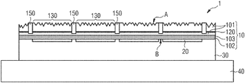
- FIG. 4 shows a further step of a method for producing an optoelectronic semiconductor component 1 according to the first non-limiting embodiment.
- the material of the optical isolator 150 is removed from the first main side A by a CMP process in such a way that the material of the optical isolators 150 is retained in the recesses 140 .
- the reflectivity of the first main side A intended for coupling out electromagnetic radiation generated in the active region 103 is advantageously reduced.
- FIG. 5 shows a further step of a method for producing an optoelectronic semiconductor component 1 according to the first non-limiting embodiment.
- the first main side A is roughened by means of a wet chemical process. A roughening reduces the waveguide effect and thus increases the coupling out probability of electromagnetic radiation generated in the active region 103 .
- FIG. 6 shows a schematic cross-section through an optoelectronic semiconductor component 1 according to a second non-limiting embodiment.
- the second non-limiting embodiment corresponds essentially to the first non-limiting embodiment shown in FIG. 5 , but differs in the type of roughening of the first main surface A.
- the first main side A is patterned by a dry chemical etching process to reduce the waveguide effect within the semiconductor body 10 .
- the structuring includes regular structuring in the form of pyramids or truncated cones.
- FIG. 7 shows a schematic cross-section of an optoelectronic semiconductor component 1 according to a third non-limiting embodiment.
- the third non-limiting embodiment is essentially similar to the first non-limiting embodiment shown in FIG. 4 .
- the position of the marker layer 120 and the position of the active region 103 are different.
- the recesses 140 extend from the first main side A through the first region 101 to the second region 102 .
- the recesses 140 completely penetrate both the active region 103 and the marker layer 120 . This results in an even better optical separation of the emission regions 130 from each other.
- regions are formed at the interfaces of the active region 103 and the recesses 140 , which are more susceptible to harmful environmental influences.
- the recesses 140 are then filled with a metal that has a high reflectivity for electromagnetic radiation generated in the active region 103 .
- FIG. 8 shows an enlarged detail of a schematic cross-section of an optoelectronic semiconductor component 1 according to a fourth non-limiting embodiment.
- the fourth non-limiting embodiment is essentially similar to the third non-limiting embodiment shown in FIG. 7 .
- the recesses 140 in which the optical isolator 150 is arranged, adjoin the marker layer 120 .
- the recesses 140 do not penetrate the marker layer 120 .
- the invention is not limited by the description based on the non-limiting embodiments. Rather, the invention comprises each new feature as well as each combination of features, which in particular includes each combination of features in the claims, even if this feature or feature combination is not itself explicitly stated in the claims or non-limiting embodiments.
Abstract
Description
-
- a semiconductor body comprising a first region of an n-type conductivity, a second region of a p-type conductivity, an active region suitable for generating electromagnetic radiation, a marker layer,
- a first main side, a second main side, a plurality of emission regions and a plurality of recesses, wherein
- the active region between the first region and the second region is arranged in a plane parallel to the main extension plane of the semiconductor body,
- the emission regions are separately controllable regions of the active region and are arranged laterally spaced apart from each other,
- the recesses delimit the emission regions in a lateral direction,
- the first main side delimits the semiconductor body on the side of the first region remote from the active region and is intended for coupling out electromagnetic radiation from the semiconductor body,
- the first main side is roughened or structured,
- the second main side delimits the semiconductor body on the side of the second region facing away from the active region,
- the marker layer is oriented parallel to the main plane of the semiconductor body,
- the recesses, starting from the first main side, extend transverse to the main extension plane of the semiconductor body in the direction of the second main side and adjoin the marker layer or may penetrate the marker layer completely, and wherein
- the recesses are only formed in the first region or the recesses extend into the second region and completely penetrate the active region.
- 1 optoelectronic semiconductor component
- 10 semiconductor body
- 101 first region
- 102 second region
- 103 active region
- A first main side
- B second main side
- 120 marker layer
- 130 emission region
- 140 recess
- 150 optical isolator
- 20 mirror layer
- 30 functional region
- 40 carrier
Claims (12)
Applications Claiming Priority (3)
| Application Number | Priority Date | Filing Date | Title |
|---|---|---|---|
| DE102018106970.7A DE102018106970A1 (en) | 2018-03-23 | 2018-03-23 | Optoelectronic semiconductor component and method for producing an optoelectronic semiconductor component |
| DE102018106970.7 | 2018-03-23 | ||
| PCT/EP2019/057203 WO2019180192A1 (en) | 2018-03-23 | 2019-03-22 | Optoelectronic semiconductor component, and method for producing an optoelectronic semiconductor component |
Publications (2)
| Publication Number | Publication Date |
|---|---|
| US20210028223A1 US20210028223A1 (en) | 2021-01-28 |
| US11404471B2 true US11404471B2 (en) | 2022-08-02 |
Family
ID=65911171
Family Applications (1)
| Application Number | Title | Priority Date | Filing Date |
|---|---|---|---|
| US17/040,084 Active US11404471B2 (en) | 2018-03-23 | 2019-03-22 | Optoelectronic semiconductor component, and method for producing an optoelectronic semiconductor component |
Country Status (3)
| Country | Link |
|---|---|
| US (1) | US11404471B2 (en) |
| DE (1) | DE102018106970A1 (en) |
| WO (1) | WO2019180192A1 (en) |
Families Citing this family (1)
| Publication number | Priority date | Publication date | Assignee | Title |
|---|---|---|---|---|
| DE102021104673A1 (en) | 2021-02-26 | 2022-09-01 | OSRAM Opto Semiconductors Gesellschaft mit beschränkter Haftung | PIXELATED LIGHT SOURCE, PROCESS AND USE |
Citations (12)
| Publication number | Priority date | Publication date | Assignee | Title |
|---|---|---|---|---|
| JP2000332290A (en) | 1999-05-20 | 2000-11-30 | Matsushita Electric Ind Co Ltd | Nitride semiconductor element and its manufacture |
| US20040104351A1 (en) * | 2002-08-09 | 2004-06-03 | Katsumi Shibayama | Photodiode array, method of making the same, and radiation detector |
| US20040173802A1 (en) | 2003-03-07 | 2004-09-09 | Hitachi Cable, Ltd. | Light-emitting diode array |
| US20060175621A1 (en) | 2001-12-28 | 2006-08-10 | Sanken Electric Co., Ltd. | Semiconductor light-emitting device light-emitting display method for manufacturing semiconductor light-emitting device and method for manufacturing light-emitting display |
| US20090068847A1 (en) * | 2007-09-12 | 2009-03-12 | Texas Instruments Inc. | Methods for removing contaminants from aluminum-comprising bond pads and integrated circuits therefrom |
| US8569084B2 (en) * | 2009-03-03 | 2013-10-29 | Lg Innotek Co., Ltd. | Method for fabricating light emitting device including photonic crystal structures |
| WO2014033041A1 (en) | 2012-08-28 | 2014-03-06 | Osram Opto Semiconductors Gmbh | Method for producing an optoelectronic semiconductor chip with reflective electrode |
| EP2816617A1 (en) | 2013-06-18 | 2014-12-24 | LSI Corporation | Semiconductor optical emitting device with metallized sidewalls |
| DE102015108532A1 (en) | 2015-05-29 | 2016-12-01 | Osram Opto Semiconductors Gmbh | Display device with a plurality of separately operable pixels |
| US20170092820A1 (en) | 2015-09-30 | 2017-03-30 | Samsung Electronics Co., Ltd. | Light emitting device package |
| DE102015119353A1 (en) | 2015-11-10 | 2017-05-11 | Osram Opto Semiconductors Gmbh | Optoelectronic semiconductor component and method for producing an optoelectronic semiconductor component |
| US20170345951A1 (en) | 2010-06-18 | 2017-11-30 | Sionyx, Llc | High Speed Photosensitive Devices and Associated Methods |
-
2018
- 2018-03-23 DE DE102018106970.7A patent/DE102018106970A1/en active Pending
-
2019
- 2019-03-22 WO PCT/EP2019/057203 patent/WO2019180192A1/en active Application Filing
- 2019-03-22 US US17/040,084 patent/US11404471B2/en active Active
Patent Citations (15)
| Publication number | Priority date | Publication date | Assignee | Title |
|---|---|---|---|---|
| JP2000332290A (en) | 1999-05-20 | 2000-11-30 | Matsushita Electric Ind Co Ltd | Nitride semiconductor element and its manufacture |
| US20060175621A1 (en) | 2001-12-28 | 2006-08-10 | Sanken Electric Co., Ltd. | Semiconductor light-emitting device light-emitting display method for manufacturing semiconductor light-emitting device and method for manufacturing light-emitting display |
| US20040104351A1 (en) * | 2002-08-09 | 2004-06-03 | Katsumi Shibayama | Photodiode array, method of making the same, and radiation detector |
| US20040173802A1 (en) | 2003-03-07 | 2004-09-09 | Hitachi Cable, Ltd. | Light-emitting diode array |
| US20090068847A1 (en) * | 2007-09-12 | 2009-03-12 | Texas Instruments Inc. | Methods for removing contaminants from aluminum-comprising bond pads and integrated circuits therefrom |
| US8569084B2 (en) * | 2009-03-03 | 2013-10-29 | Lg Innotek Co., Ltd. | Method for fabricating light emitting device including photonic crystal structures |
| US20170345951A1 (en) | 2010-06-18 | 2017-11-30 | Sionyx, Llc | High Speed Photosensitive Devices and Associated Methods |
| WO2014033041A1 (en) | 2012-08-28 | 2014-03-06 | Osram Opto Semiconductors Gmbh | Method for producing an optoelectronic semiconductor chip with reflective electrode |
| US20150255692A1 (en) | 2012-08-28 | 2015-09-10 | Osram Opto Semiconductors Gmbh | Method for Producing an Optoelectronic Semiconductor Chip with Reflective Electrode |
| EP2816617A1 (en) | 2013-06-18 | 2014-12-24 | LSI Corporation | Semiconductor optical emitting device with metallized sidewalls |
| DE102015108532A1 (en) | 2015-05-29 | 2016-12-01 | Osram Opto Semiconductors Gmbh | Display device with a plurality of separately operable pixels |
| US20180166499A1 (en) | 2015-05-29 | 2018-06-14 | Osram Opto Semiconductors Gmbh | Display Device Having a Plurality of Pixels that can be Operated Separately from One Another |
| US20170092820A1 (en) | 2015-09-30 | 2017-03-30 | Samsung Electronics Co., Ltd. | Light emitting device package |
| DE102015119353A1 (en) | 2015-11-10 | 2017-05-11 | Osram Opto Semiconductors Gmbh | Optoelectronic semiconductor component and method for producing an optoelectronic semiconductor component |
| US20180331251A1 (en) | 2015-11-10 | 2018-11-15 | Osram Opto Semiconductors Gmbh | Optoelectronic Semiconductor Component and Method for Producing an Optoelectronic Semiconductor Component |
Non-Patent Citations (1)
| Title |
|---|
| International Search Report issued for the corresponding international application No. PCT/EP2019/057203, dated Jun. 7, 2019, 4 pages (for informational purpose only). |
Also Published As
| Publication number | Publication date |
|---|---|
| DE102018106970A1 (en) | 2019-09-26 |
| US20210028223A1 (en) | 2021-01-28 |
| WO2019180192A1 (en) | 2019-09-26 |
Similar Documents
| Publication | Publication Date | Title |
|---|---|---|
| US10916579B2 (en) | Optoelectronic device with light-emitting diodes | |
| CN103477452B (en) | Opto-electronic semiconductor chip | |
| KR101258583B1 (en) | Nano lod light emitting device and method of manufacturing the same | |
| US8093607B2 (en) | Optoelectronic semiconductor component | |
| FR3053530A1 (en) | PIXEL OPTOELECTRONIC DEVICE WITH IMPROVED CONTRAST AND LUMINANCE | |
| EP3373344B1 (en) | Optoelectronic device comprising light-emitting diodes with improved light extraction | |
| KR20110030542A (en) | Method for producing an optoelectronic component and optoelectronic component | |
| US10916580B2 (en) | Optoelectronic device with light-emitting diodes | |
| JP2010541216A (en) | Optoelectronic semiconductor body | |
| US9530935B2 (en) | Method for fabricating a plurality of opto-electronic semiconductor chips, and opto-electronic semiconductor chip | |
| US10381521B2 (en) | Optoelectronic component and method for producing an optoelectronic component | |
| KR20220140749A (en) | Red LEDs and how to make them | |
| CN110313069B (en) | Optoelectronic device with light emitting diode | |
| JP2017512380A (en) | Method for manufacturing semiconductor component and semiconductor component | |
| KR20210006373A (en) | Process for manufacturing optoelectronic devices with diode matrix | |
| US11063182B2 (en) | Optoelectronic component and method of manufacturing an optoelectronic component | |
| KR20230058638A (en) | LED devices and methods of manufacturing LED devices | |
| EP3384531B1 (en) | Optoelectronic device comprising a light-emitting component and a transistor | |
| US11404471B2 (en) | Optoelectronic semiconductor component, and method for producing an optoelectronic semiconductor component | |
| JP7418583B2 (en) | Method of forming monolithic light emitting diode precursors | |
| US11177414B2 (en) | Optoelectronic component and method for producing an optoelectronic component | |
| US20220336701A1 (en) | Semiconductor Chip and Method for Producing a Semiconductor Chip | |
| TWI594455B (en) | Photoelectric semiconductor chip and its manufacturing method | |
| US20230047118A1 (en) | Radiation-emitting semiconductor chip and method for producing a radiation-emitting semiconductor chip | |
| KR102658970B1 (en) | Optoelectronic device having a diode array |
Legal Events
| Date | Code | Title | Description |
|---|---|---|---|
| FEPP | Fee payment procedure |
Free format text: ENTITY STATUS SET TO UNDISCOUNTED (ORIGINAL EVENT CODE: BIG.); ENTITY STATUS OF PATENT OWNER: LARGE ENTITY |
|
| AS | Assignment |
Owner name: OSRAM OLED GMBH, GERMANY Free format text: ASSIGNMENT OF ASSIGNORS INTEREST;ASSIGNORS:MUELLER, CHRISTIAN;SCHOLZ, DOMINIK;HERTKORN, JOACHIM;SIGNING DATES FROM 20200930 TO 20201008;REEL/FRAME:054172/0397 |
|
| STPP | Information on status: patent application and granting procedure in general |
Free format text: APPLICATION DISPATCHED FROM PREEXAM, NOT YET DOCKETED |
|
| STPP | Information on status: patent application and granting procedure in general |
Free format text: DOCKETED NEW CASE - READY FOR EXAMINATION |
|
| STPP | Information on status: patent application and granting procedure in general |
Free format text: NON FINAL ACTION MAILED |
|
| STPP | Information on status: patent application and granting procedure in general |
Free format text: RESPONSE TO NON-FINAL OFFICE ACTION ENTERED AND FORWARDED TO EXAMINER |
|
| STPP | Information on status: patent application and granting procedure in general |
Free format text: FINAL REJECTION MAILED |
|
| STPP | Information on status: patent application and granting procedure in general |
Free format text: RESPONSE AFTER FINAL ACTION FORWARDED TO EXAMINER |
|
| STPP | Information on status: patent application and granting procedure in general |
Free format text: NOTICE OF ALLOWANCE MAILED -- APPLICATION RECEIVED IN OFFICE OF PUBLICATIONS |
|
| STCF | Information on status: patent grant |
Free format text: PATENTED CASE |