EP3065295A1 - Overcurrent protection circuit - Google Patents
Overcurrent protection circuit Download PDFInfo
- Publication number
- EP3065295A1 EP3065295A1 EP14858024.4A EP14858024A EP3065295A1 EP 3065295 A1 EP3065295 A1 EP 3065295A1 EP 14858024 A EP14858024 A EP 14858024A EP 3065295 A1 EP3065295 A1 EP 3065295A1
- Authority
- EP
- European Patent Office
- Prior art keywords
- switching element
- circuit
- overcurrent protection
- protection circuit
- time period
- Prior art date
- Legal status (The legal status is an assumption and is not a legal conclusion. Google has not performed a legal analysis and makes no representation as to the accuracy of the status listed.)
- Granted
Links
- 238000001514 detection method Methods 0.000 claims abstract description 27
- 210000000352 storage cell Anatomy 0.000 claims description 11
- 238000010586 diagram Methods 0.000 description 11
- 230000001052 transient effect Effects 0.000 description 7
- 230000015556 catabolic process Effects 0.000 description 3
- 239000004065 semiconductor Substances 0.000 description 3
- 230000007423 decrease Effects 0.000 description 2
- 230000005669 field effect Effects 0.000 description 2
- 229910044991 metal oxide Inorganic materials 0.000 description 2
- 150000004706 metal oxides Chemical class 0.000 description 2
- 230000005856 abnormality Effects 0.000 description 1
- 230000003247 decreasing effect Effects 0.000 description 1
- 230000000694 effects Effects 0.000 description 1
- 230000007257 malfunction Effects 0.000 description 1
Images


Classifications
-
- H—ELECTRICITY
- H03—ELECTRONIC CIRCUITRY
- H03K—PULSE TECHNIQUE
- H03K17/00—Electronic switching or gating, i.e. not by contact-making and –breaking
- H03K17/08—Modifications for protecting switching circuit against overcurrent or overvoltage
- H03K17/082—Modifications for protecting switching circuit against overcurrent or overvoltage by feedback from the output to the control circuit
- H03K17/0822—Modifications for protecting switching circuit against overcurrent or overvoltage by feedback from the output to the control circuit in field-effect transistor switches
-
- H—ELECTRICITY
- H02—GENERATION; CONVERSION OR DISTRIBUTION OF ELECTRIC POWER
- H02H—EMERGENCY PROTECTIVE CIRCUIT ARRANGEMENTS
- H02H11/00—Emergency protective circuit arrangements for preventing the switching-on in case an undesired electric working condition might result
- H02H11/006—Emergency protective circuit arrangements for preventing the switching-on in case an undesired electric working condition might result in case of too high or too low voltage
-
- H—ELECTRICITY
- H02—GENERATION; CONVERSION OR DISTRIBUTION OF ELECTRIC POWER
- H02H—EMERGENCY PROTECTIVE CIRCUIT ARRANGEMENTS
- H02H3/00—Emergency protective circuit arrangements for automatic disconnection directly responsive to an undesired change from normal electric working condition with or without subsequent reconnection ; integrated protection
- H02H3/20—Emergency protective circuit arrangements for automatic disconnection directly responsive to an undesired change from normal electric working condition with or without subsequent reconnection ; integrated protection responsive to excess voltage
-
- H—ELECTRICITY
- H03—ELECTRONIC CIRCUITRY
- H03K—PULSE TECHNIQUE
- H03K17/00—Electronic switching or gating, i.e. not by contact-making and –breaking
- H03K17/18—Modifications for indicating state of switch
-
- H—ELECTRICITY
- H03—ELECTRONIC CIRCUITRY
- H03K—PULSE TECHNIQUE
- H03K2217/00—Indexing scheme related to electronic switching or gating, i.e. not by contact-making or -breaking covered by H03K17/00
- H03K2217/0027—Measuring means of, e.g. currents through or voltages across the switch
Definitions
- the present invention relates to an overcurrent protection circuit that detects, when a switching element is on, a differential voltage value between both ends of the switching element that is caused by a current flowing therethrough, and turns off the switching element when the detected differential voltage value is larger than a predetermined voltage value.
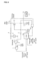
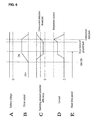
- FIG. 5 is a circuit diagram illustrating an example of a configuration of the main parts of a conventional overcurrent protection circuit for use in a vehicle.
- This overcurrent protection circuit is a circuit that protects a switching element 7 connected between the plus electrode of a battery 11 and the supply terminal of the load 10.
- the ground terminal of the load 10 is grounded.
- the switching element 7 has a configuration in which the source of an N-channel MOSFET (metal-oxide semiconductor field-effect transistor) 8 whose drain is connected to the plus electrode of the battery 11, and the source of an N-channel MOSFET 9 whose drain is connected to the load are adjacent and connected to each other.
- the FETs 8 and 9 are drive-controlled by a driver (driving circuit) 5 so as to be turned on or off at the same time.
- a resistor 4 is connected to the plus electrode of the battery 11, and the other end of the resistor 4 is connected to the input terminal of a constant current circuit 3 and the non-inverting input terminal of a comparator 2.
- the output terminal of the constant current circuit 3 is grounded, and the inverting input terminal of the comparator 2 is connected to the supply terminal of the load 10 via a resistor 6.
- the output terminal of the comparator 2 is connected to one input terminal of an AND circuit 1, an inverted signal of a mask signal is input to the other input terminal of the AND circuit 1, and an output of the AND circuit 1 is given to the driver (driving circuit) 5.
- the mask signal, and a command signal for the driver are given from a not-shown ECU (Electronic Control Unit) of the load 10.
- the constant current circuit 3 generates a threshold voltage of a drop voltage by letting a constant current flow through the resistor 4.
- the comparator 2 needs only to output a plus signal so as to stop the driver 5.
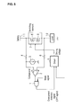
- a differential voltage value between both ends of the switching element 7 (a switching element potential difference of FIGS. 6C and 7C ) is at the level of the voltage value of the battery 11 and exceeds the threshold voltage. Therefore, a mask time period ( FIGS. 6E and 7E ) in which output of the comparator 2 is disabled needs to be provided for a time period in which the switching element 7 is off, and a time period in which the state of the switching element 7 is transient from off to on.
- the mask time period is configured such that an inverted signal of a mask signal is given to the other input terminal of the AND circuit 1, and thus, during the mask time period, the AND circuit 1 continues to output an L-level signal and does not stop the driver 5 even when the output signal of the comparator 2 becomes positive.
- this overcurrent protection circuit when the output of the driver 5 is off ( FIGS. 6B and 7B ), a mask signal is applied to realize the mask time period ( FIGS. 6E and 7E ), and thus the output signal of the comparator 2 is disabled although the differential voltage value between both ends of the switching element 7 (switching element potential difference of FIGS. 6C and 7C ) exceeds the threshold voltage (overcurrent detection threshold).
- a mask signal is applied to realize the mask time period ( FIG. 6E ), and thus the output signal of the comparator 2 is disabled although the differential voltage value between both ends of the switching element 7 (switching element potential difference of FIG. 6C ) exceeds the threshold voltage (overcurrent detection threshold).
- a time period in which the output of the driver 5 steadily remains on ( FIG. 6B ) serves as a non-mask time period since no mask signal is applied ( FIG. 6E ).
- Patent Document 1 discloses a load circuit overcurrent protection device that is capable of highly accurate overcurrent detection without being affected by an on-resistance deviation ⁇ Ron of a semiconductor element.
- Patent Document 1 JP 2009-296367A
- the differential voltage value between both ends of the switching element 7 ( FIG. 7C ) is maintained substantially at: (output voltage value of the battery 11) - (threshold voltage for overcurrent detection).
- the above-described overcurrent protection circuit has one power supply system, but the same problem is caused even when the switching element is connected between, for example, a main battery and a sub (subordinate) battery.
- the present invention was made in view of the above-described circumstances, and it is an object of the prevent invention to provide an overcurrent protection circuit that can cope even with a case where a ground fault occurs in a mask time period for overcurrent detection.
- an overcurrent protection circuit for detecting, when a switching element is on, a differential voltage value between both ends of the switching element that is caused by an electric current flowing through the switching element, and turning off the switching element when the detected differential voltage value is larger than a predetermined voltage value, includes: a detection circuit for detecting respective voltage values at the both ends; and means for preventing the switching element from being turned on if either of the respective voltage values detected by the detection circuit is less than the predetermined value.
- this overcurrent protection circuit when the switching element is on, a differential voltage value between both ends of the switching element that is caused by a current flowing therethrough is detected, and the switching element is turned off when the detected differential voltage value is larger than a predetermined voltage value.
- the detection circuit detects respective voltage values at both ends of the switching element, and if either of the respective voltage values detected by the detection circuit is less than the predetermined value, the preventing means prevents the switching element from being turned on.
- the overcurrent protection circuit may be such that the detection circuit is a NAND circuit or an AND circuit to which the respective voltage values at the both ends are input.
- the detection circuit is a NAND circuit or an AND circuit to which the respective voltage values at the both ends of the switching element are input, it is possible to determine whether or not either of the voltage values is less than the predetermined value without detecting the respective voltage values at the both ends of the switching element using a detecting device.
- the overcurrent protection circuit may be such that the switching element is connected between a main storage cell and an auxiliary storage device that is auxiliary to the main storage cell, and the voltage values at the both ends are respective output voltage values of the main storage cell and the auxiliary storage device.
- the switching element is connected between the main storage cell and the auxiliary storage device that is auxiliary to the main storage cell, and the voltage values between both ends of the switching element are respective output voltage values of the main storage cell and the auxiliary storage device.
- an overcurrent protection circuit that can cope even with a case where a ground fault occurs in a mask time period for overcurrent detection. Furthermore, since the ground fault state can be detected before the switching element is turned on, there is no need for taking into consideration overcurrent detection during the time period in which the switching element 7 is transient from off to on, and thus the mask time period for overcurrent detection is easily set (can be set to be larger), making it possible to prevent a malfunction.
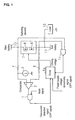
- FIG. 1 is a circuit diagram illustrating a configuration of the main parts of an overcurrent protection circuit according to an embodiment of the present invention.
- This overcurrent protection circuit is a circuit that protects a switching element 7 connected between the plus electrode of a main battery (main storage cell) 12 and the plus electrode of a sub battery (auxiliary storage device) 13.
- the supply terminal of a load 10 is connected to the plus electrode of the sub battery 13, and the ground terminal of the load 10 is grounded.
- the switching element 7 has a configuration in which the source of an N-channel MOSFET (metal-oxide semiconductor field-effect transistor) 8 whose drain is connected to the plus electrode of the main battery 12, and the source of an N-channel MOSFET 9 whose drain is connected to the plus electrode of the sub battery 13 are adjacent and connected to each other.
- the FETs 8 and 9 are drive-controlled by a driver (driving circuit) 5a so as to be turned on or off at the same time.
- a resistor 4 is connected to the plus electrode of the main battery 12, and the other end of the resistor 4 is connected to the input terminal of a constant current circuit 3 and the non-inverting input terminal of a comparator 2.
- the output terminal of the constant current circuit 3 is grounded, and the inverting input terminal of the comparator 2 is connected to the plus electrode of the sub battery 13 via a resistor 6.
- the output terminal of the comparator 2 is connected to one input terminal of an AND circuit 1, an inverted signal of a mask signal is input to the other input terminal of the AND circuit 1, and an output of the AND circuit 1 is given to the driver (driving circuit) 5a.
- the mask signal, and a command signal for the driver are provided by a not-shown ECU (Electronic Control Unit) of the power supply system.
- the plus electrode of the main battery 12 and the plus electrode of the sub battery 13 are respectively connected to the input terminals of a NAND circuit (preventing means) 14, and an output signal of the NAND circuit 14 is given to the driver 5a.
- the NAND circuit 14 can be replaced by an AND circuit depending on a configuration of the driver 5a.
- the constant current circuit 3 generates a threshold voltage of a drop voltage by letting a constant current flow through the resistor 4.
- the comparator 2 needs only to output a plus signal so as to stop the driver 5a.
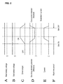
- a differential voltage value between both ends of the switching element 7 (a switching element potential difference of FIGS. 2D and 3D ) is a difference between an output voltage of the main battery 12 ( FIGS. 2A and 3A ) and an output voltage of the sub battery 13 ( FIGS. 2B and 3B ), and may exceed the threshold voltage. Therefore, a mask time period ( FIGS. 2F and 3F ) in which output of the comparator 2 is disabled needs to be provided for a time period in which the switching element 7 is off and a time period in which the state of the switching element 7 is transient from off to on.
- the mask time period is configured such that an inverted signal of a mask signal is given to the other input terminal of the AND circuit 1, and thus, during the mask time period, the AND circuit 1 continues to output an L-level signal and does not stop the driver 5a even when the output signal of the comparator 2 becomes positive.
- this overcurrent protection circuit when the output of the driver 5a is off ( FIGS. 2C and 3C ), a mask signal is applied to realize the mask time period ( FIGS. 2F and 3F ), and thus the output signal of the comparator 2 is disabled although the differential voltage value between both ends of the switching element 7 (switching element potential difference of FIGS. 2D and 3D ) exceeds the threshold voltage (overcurrent detection threshold).
- a mask signal is applied to realize the mask time period ( FIG. 2F ), and the output signal of the comparator 2 is disabled although the differential voltage value between both ends of the switching element 7 (switching element potential difference of FIG. 2D ) exceeds the threshold voltage (overcurrent detection threshold).
- a time period in which the output of the driver 5a steadily remains on ( FIG. 2C ) serves as a non-mask time period since no mask signal is applied ( FIG. 2F ).
- the NAND circuit 14 has an H-level input from the main battery 12 side and an L-level input from the sub battery 13, and gives an H-level power-supply voltage abnormality signal to the driver 5a, preventing the operation of the driver 5a ( FIG. 3C ). As a result, the switching element 7 is protected since no current flows ( FIG. 3E ) therethrough.
- the switching element 7 has a configuration in which the sources of the FETs 8 and 9 are adjacent and connected to each other, but the switching element 7 may be replaced by an N-channel MOSFET 15, as shown in FIG. 4 .
- the FET 15 is connected with its source to the plus electrode of the sub battery 13, and is connected with its drain to the plus electrode of the main battery 12.
- the present invention is applicable to an overcurrent protection circuit that can turn off a switching element when an overcurrent flows through the switching element, protecting the switching element.
Abstract
Description
- The present invention relates to an overcurrent protection circuit that detects, when a switching element is on, a differential voltage value between both ends of the switching element that is caused by a current flowing therethrough, and turns off the switching element when the detected differential voltage value is larger than a predetermined voltage value.
-
FIG. 5 is a circuit diagram illustrating an example of a configuration of the main parts of a conventional overcurrent protection circuit for use in a vehicle. - This overcurrent protection circuit is a circuit that protects a switching element 7 connected between the plus electrode of a
battery 11 and the supply terminal of theload 10. The ground terminal of theload 10 is grounded. - The switching element 7 has a configuration in which the source of an N-channel MOSFET (metal-oxide semiconductor field-effect transistor) 8 whose drain is connected to the plus electrode of the
battery 11, and the source of an N-channel MOSFET 9 whose drain is connected to the load are adjacent and connected to each other. The FETs 8 and 9 are drive-controlled by a driver (driving circuit) 5 so as to be turned on or off at the same time. - Furthermore, one end of a
resistor 4 is connected to the plus electrode of thebattery 11, and the other end of theresistor 4 is connected to the input terminal of a constant current circuit 3 and the non-inverting input terminal of acomparator 2. The output terminal of the constant current circuit 3 is grounded, and the inverting input terminal of thecomparator 2 is connected to the supply terminal of theload 10 via aresistor 6. - The output terminal of the
comparator 2 is connected to one input terminal of anAND circuit 1, an inverted signal of a mask signal is input to the other input terminal of theAND circuit 1, and an output of theAND circuit 1 is given to the driver (driving circuit) 5. The mask signal, and a command signal for the driver are given from a not-shown ECU (Electronic Control Unit) of theload 10. - Hereinafter, examples of operations of an overcurrent protection circuit having such a configuration will be described with reference to the timing diagrams of
FIGS. 6 and7 showing that example. - Note that the output voltage value of the
battery 11 is assumed to be constant (FIGS. 6A and7A ). - The constant current circuit 3 generates a threshold voltage of a drop voltage by letting a constant current flow through the
resistor 4. When an overcurrent flows through the switching element 7, and the value of a drop voltage caused by the on-resistance of the switching element 7 increases to a value larger than the value of the drop voltage generated by the constant current of the resistor 4 (the voltage value itself decreases), thecomparator 2 needs only to output a plus signal so as to stop thedriver 5. - However, when the switching element 7 is off (
FIGS. 6B and7B ), a differential voltage value between both ends of the switching element 7 (a switching element potential difference ofFIGS. 6C and7C ) is at the level of the voltage value of thebattery 11 and exceeds the threshold voltage. Therefore, a mask time period (FIGS. 6E and7E ) in which output of thecomparator 2 is disabled needs to be provided for a time period in which the switching element 7 is off, and a time period in which the state of the switching element 7 is transient from off to on. - In this overcurrent protection circuit, the mask time period is configured such that an inverted signal of a mask signal is given to the other input terminal of the
AND circuit 1, and thus, during the mask time period, theAND circuit 1 continues to output an L-level signal and does not stop thedriver 5 even when the output signal of thecomparator 2 becomes positive. - Accordingly, in this overcurrent protection circuit, when the output of the
driver 5 is off (FIGS. 6B and7B ), a mask signal is applied to realize the mask time period (FIGS. 6E and7E ), and thus the output signal of thecomparator 2 is disabled although the differential voltage value between both ends of the switching element 7 (switching element potential difference ofFIGS. 6C and7C ) exceeds the threshold voltage (overcurrent detection threshold). - Also in the transient time period in which the output of the
driver 5 changes from off to on (FIG. 6B ), a mask signal is applied to realize the mask time period (FIG. 6E ), and thus the output signal of thecomparator 2 is disabled although the differential voltage value between both ends of the switching element 7 (switching element potential difference ofFIG. 6C ) exceeds the threshold voltage (overcurrent detection threshold). - A time period in which the output of the
driver 5 steadily remains on (FIG. 6B ) serves as a non-mask time period since no mask signal is applied (FIG. 6E ). - In this state, if a ground fault occurs in the
load 10 on the supply terminal side (FIG. 6D ), the current flowing through the switching element 7 will increase (FIG. 6D ) and the differential voltage value between both ends of the switching element 7 (FIG. 6C ) will exceed the threshold voltage (overcurrent detection threshold). Accordingly, thecomparator 2 outputs a plus signal, theAND circuit 1 outputs an H-level overcurrent detection signal, the output signal of thedriver 5 changes from on to off (FIG. 6B ), and the current flowing through the switching element 7 starts decreasing before reaching a breakdown current and eventually takes on zero (FIG. 6D ). -
Patent Document 1 discloses a load circuit overcurrent protection device that is capable of highly accurate overcurrent detection without being affected by an on-resistance deviation ±ΔRon of a semiconductor element. - Patent Document 1:
JP 2009-296367A - As described above, in the conventional overcurrent protection circuit, since the time period in which the switching element 7 is off and the time period in which the state of the switching element 7 is transient from off to on serve as the mask time period (
FIG. 6E ), no false detection is caused. However, there is the problem that even if a ground fault occurs in theload 10 on the supply terminal side in the time period in which the switching element 7 is off, which serves as the mask time period (FIG. 7E ), and then the current flowing through the switching element 7 increase during the time period in which the state of the switching element 7 is transient from off to on, which serves as the mask time period, no overcurrent can be detected and the current may reach the breakdown current (FIG. 7D ). - Note that since the ground fault occurs in the
load 10 on the supply terminal side, the differential voltage value between both ends of the switching element 7 (FIG. 7C ) is maintained substantially at: (output voltage value of the battery 11) - (threshold voltage for overcurrent detection). - The above-described overcurrent protection circuit has one power supply system, but the same problem is caused even when the switching element is connected between, for example, a main battery and a sub (subordinate) battery.
- The present invention was made in view of the above-described circumstances, and it is an object of the prevent invention to provide an overcurrent protection circuit that can cope even with a case where a ground fault occurs in a mask time period for overcurrent detection.
- According to a first aspect, an overcurrent protection circuit for detecting, when a switching element is on, a differential voltage value between both ends of the switching element that is caused by an electric current flowing through the switching element, and turning off the switching element when the detected differential voltage value is larger than a predetermined voltage value, includes: a detection circuit for detecting respective voltage values at the both ends; and means for preventing the switching element from being turned on if either of the respective voltage values detected by the detection circuit is less than the predetermined value.
- In this overcurrent protection circuit, when the switching element is on, a differential voltage value between both ends of the switching element that is caused by a current flowing therethrough is detected, and the switching element is turned off when the detected differential voltage value is larger than a predetermined voltage value. The detection circuit detects respective voltage values at both ends of the switching element, and if either of the respective voltage values detected by the detection circuit is less than the predetermined value, the preventing means prevents the switching element from being turned on.
- According to a second aspect, the overcurrent protection circuit may be such that the detection circuit is a NAND circuit or an AND circuit to which the respective voltage values at the both ends are input.
- In the overcurrent protection circuit, since the detection circuit is a NAND circuit or an AND circuit to which the respective voltage values at the both ends of the switching element are input, it is possible to determine whether or not either of the voltage values is less than the predetermined value without detecting the respective voltage values at the both ends of the switching element using a detecting device.
- According to a third aspect, the overcurrent protection circuit may be such that the switching element is connected between a main storage cell and an auxiliary storage device that is auxiliary to the main storage cell, and the voltage values at the both ends are respective output voltage values of the main storage cell and the auxiliary storage device.
- In the overcurrent protection circuit, the switching element is connected between the main storage cell and the auxiliary storage device that is auxiliary to the main storage cell, and the voltage values between both ends of the switching element are respective output voltage values of the main storage cell and the auxiliary storage device.
- According to the present invention, it is possible to realize an overcurrent protection circuit that can cope even with a case where a ground fault occurs in a mask time period for overcurrent detection. Furthermore, since the ground fault state can be detected before the switching element is turned on, there is no need for taking into consideration overcurrent detection during the time period in which the switching element 7 is transient from off to on, and thus the mask time period for overcurrent detection is easily set (can be set to be larger), making it possible to prevent a malfunction.
-
-
FIG. 1 is a circuit diagram illustrating a configuration of the main parts of an overcurrent protection circuit according to an embodiment of the present invention. -
FIG. 2 is a timing diagram illustrating an example of an operation of the overcurrent protection circuit shown inFIG. 1 . -
FIG. 3 is a timing diagram illustrating an example of an operation of the overcurrent protection circuit shown inFIG. 1 . -
FIG. 4 is a circuit diagram illustrating another configuration of the main parts of the overcurrent protection circuit according to the embodiment of the present invention. -
FIG. 5 is a circuit diagram illustrating an example of a configuration of the main parts of a conventional overcurrent protection circuit. -
FIG. 6 is a timing diagram illustrating an example of an operation of the overcurrent protection circuit shown inFIG. 5 . -
FIG. 7 is a timing diagram illustrating an example of an operation of the overcurrent protection circuit shown inFIG. 5 . - Hereinafter, the present invention will be described with reference to the drawings illustrating embodiment thereof.
-
FIG. 1 is a circuit diagram illustrating a configuration of the main parts of an overcurrent protection circuit according to an embodiment of the present invention. - This overcurrent protection circuit is a circuit that protects a switching element 7 connected between the plus electrode of a main battery (main storage cell) 12 and the plus electrode of a sub battery (auxiliary storage device) 13. The supply terminal of a
load 10 is connected to the plus electrode of thesub battery 13, and the ground terminal of theload 10 is grounded. - The switching element 7 has a configuration in which the source of an N-channel MOSFET (metal-oxide semiconductor field-effect transistor) 8 whose drain is connected to the plus electrode of the
main battery 12, and the source of an N-channel MOSFET 9 whose drain is connected to the plus electrode of thesub battery 13 are adjacent and connected to each other. The FETs 8 and 9 are drive-controlled by a driver (driving circuit) 5a so as to be turned on or off at the same time. - Furthermore, one end of a
resistor 4 is connected to the plus electrode of themain battery 12, and the other end of theresistor 4 is connected to the input terminal of a constant current circuit 3 and the non-inverting input terminal of acomparator 2. The output terminal of the constant current circuit 3 is grounded, and the inverting input terminal of thecomparator 2 is connected to the plus electrode of thesub battery 13 via aresistor 6. - The output terminal of the
comparator 2 is connected to one input terminal of an ANDcircuit 1, an inverted signal of a mask signal is input to the other input terminal of the ANDcircuit 1, and an output of the ANDcircuit 1 is given to the driver (driving circuit) 5a. The mask signal, and a command signal for the driver are provided by a not-shown ECU (Electronic Control Unit) of the power supply system. - The plus electrode of the
main battery 12 and the plus electrode of thesub battery 13 are respectively connected to the input terminals of a NAND circuit (preventing means) 14, and an output signal of theNAND circuit 14 is given to the driver 5a. Note that theNAND circuit 14 can be replaced by an AND circuit depending on a configuration of the driver 5a. - Hereinafter, examples of operations of an overcurrent protection circuit having such a configuration will be described with reference to the timing diagrams of
FIGS. 2 and3 . - The constant current circuit 3 generates a threshold voltage of a drop voltage by letting a constant current flow through the
resistor 4. When an overcurrent flows through the switching element 7, and the value of a drop voltage caused by the on-resistance of the switching element 7 increases to a value that is larger than the value of the drop voltage generated by the constant current of the resistor 4 (the voltage value itself decreases), thecomparator 2 needs only to output a plus signal so as to stop the driver 5a. - However, when the switching element 7 is off (
FIGS. 2C and3C ), a differential voltage value between both ends of the switching element 7 (a switching element potential difference ofFIGS. 2D and3D ) is a difference between an output voltage of the main battery 12 (FIGS. 2A and3A ) and an output voltage of the sub battery 13 (FIGS. 2B and3B ), and may exceed the threshold voltage. Therefore, a mask time period (FIGS. 2F and3F ) in which output of thecomparator 2 is disabled needs to be provided for a time period in which the switching element 7 is off and a time period in which the state of the switching element 7 is transient from off to on. - In this overcurrent protection circuit, the mask time period is configured such that an inverted signal of a mask signal is given to the other input terminal of the AND
circuit 1, and thus, during the mask time period, the ANDcircuit 1 continues to output an L-level signal and does not stop the driver 5a even when the output signal of thecomparator 2 becomes positive. - Accordingly, in this overcurrent protection circuit, when the output of the driver 5a is off (
FIGS. 2C and3C ), a mask signal is applied to realize the mask time period (FIGS. 2F and3F ), and thus the output signal of thecomparator 2 is disabled although the differential voltage value between both ends of the switching element 7 (switching element potential difference ofFIGS. 2D and3D ) exceeds the threshold voltage (overcurrent detection threshold). - Also in the transient time period (
FIG. 2C ) in which the output of the driver 5a changes from off to on, a mask signal is applied to realize the mask time period (FIG. 2F ), and the output signal of thecomparator 2 is disabled although the differential voltage value between both ends of the switching element 7 (switching element potential difference ofFIG. 2D ) exceeds the threshold voltage (overcurrent detection threshold). - A time period in which the output of the driver 5a steadily remains on (
FIG. 2C ) serves as a non-mask time period since no mask signal is applied (FIG. 2F ). - In this state, if a ground fault occurs in the
load 10 on the supply terminal side, the current flowing through the switching element 7 increases, and a differential voltage value between both ends of the switching element 7 exceeds the threshold voltage (overcurrent detection threshold). Accordingly, thecomparator 2 outputs a plus signal, the ANDcircuit 1 outputs an H-level overcurrent detection signal, the output signal of the driver 5a changes from on to off, and the current flowing through the switching element 7 takes on zero without reaching a breakdown current. - If a ground fault occurs in the
load 10 on the supply terminal (FIG. 3B ) in the time period in which the switching element 7 is off, which serves as the mask time period (FIG. 3F ), the differential voltage value between both ends of the switching element 7 (FIG. 3D ) increases to the level of the output voltage of themain battery 12, and the output signal of thecomparator 2 becomes positive but is disabled since it is in the mask time period (FIG. 3F ). - On the other hand, the
NAND circuit 14 has an H-level input from themain battery 12 side and an L-level input from thesub battery 13, and gives an H-level power-supply voltage abnormality signal to the driver 5a, preventing the operation of the driver 5a (FIG. 3C ). As a result, the switching element 7 is protected since no current flows (FIG. 3E ) therethrough. - Note that in the present embodiment, the switching element 7 has a configuration in which the sources of the FETs 8 and 9 are adjacent and connected to each other, but the switching element 7 may be replaced by an N-
channel MOSFET 15, as shown inFIG. 4 . TheFET 15 is connected with its source to the plus electrode of thesub battery 13, and is connected with its drain to the plus electrode of themain battery 12. - The present invention is applicable to an overcurrent protection circuit that can turn off a switching element when an overcurrent flows through the switching element, protecting the switching element.
-
- 1
- AND circuit
- 2
- Comparator
- 3
- Constant current circuit
- 4, 6
- Resistor
- 5a
- Driver
- 7
- Switching element
- 8, 9, 15
- FET
- 10
- Load
- 12
- Main battery (main storage cell)
- 13
- Sub battery (auxiliary storage device)
- 14
- NAND circuit (preventing means)
Claims (3)
- An overcurrent protection circuit for detecting, when a switching element is on, a differential voltage value between both ends of the switching element that is caused by an electric current flowing through the switching element, and turning off the switching element when the detected differential voltage value is larger than a predetermined voltage value, the overcurrent protection circuit comprising:a detection circuit for detecting respective voltage values at the both ends; andmeans for preventing the switching element from being turned on if either of the respective voltage values detected by the detection circuit is less than the predetermined value.
- The overcurrent protection circuit according to claim 1,
wherein the detection circuit is a NAND circuit or an AND circuit to which the respective voltage values at the both ends are input. - The overcurrent protection circuit according to claim 1 or 2,
wherein the switching element is connected between a main storage cell and an auxiliary storage device that is auxiliary to the main storage cell, and the voltage values at the both ends are respective output voltage values of the main storage cell and the auxiliary storage device.
Applications Claiming Priority (2)
| Application Number | Priority Date | Filing Date | Title |
|---|---|---|---|
| JP2013225832A JP6322957B2 (en) | 2013-10-30 | 2013-10-30 | Overcurrent protection circuit |
| PCT/JP2014/077661 WO2015064386A1 (en) | 2013-10-30 | 2014-10-17 | Overcurrent protection circuit |
Publications (3)
| Publication Number | Publication Date |
|---|---|
| EP3065295A1 true EP3065295A1 (en) | 2016-09-07 |
| EP3065295A4 EP3065295A4 (en) | 2016-10-19 |
| EP3065295B1 EP3065295B1 (en) | 2019-08-07 |
Family
ID=53003995
Family Applications (1)
| Application Number | Title | Priority Date | Filing Date |
|---|---|---|---|
| EP14858024.4A Active EP3065295B1 (en) | 2013-10-30 | 2014-10-17 | Overcurrent protection circuit |
Country Status (5)
| Country | Link |
|---|---|
| US (1) | US10181846B2 (en) |
| EP (1) | EP3065295B1 (en) |
| JP (1) | JP6322957B2 (en) |
| CN (1) | CN105637762B (en) |
| WO (1) | WO2015064386A1 (en) |
Cited By (1)
| Publication number | Priority date | Publication date | Assignee | Title |
|---|---|---|---|---|
| CN117394698A (en) * | 2023-12-13 | 2024-01-12 | 深圳市芯茂微电子有限公司 | H-bridge power supply circuit control method, device and medium |
Families Citing this family (2)
| Publication number | Priority date | Publication date | Assignee | Title |
|---|---|---|---|---|
| CN208174241U (en) * | 2017-02-17 | 2018-11-30 | 杰华特微电子(杭州)有限公司 | A kind of leakage protection circuit |
| CN112290782B (en) * | 2020-12-21 | 2021-03-05 | 上海芯龙半导体技术股份有限公司南京分公司 | Drive signal control circuit and switching power supply chip |
Family Cites Families (11)
| Publication number | Priority date | Publication date | Assignee | Title |
|---|---|---|---|---|
| JPH04134271A (en) * | 1990-09-27 | 1992-05-08 | Nec Corp | Output circuit |
| JPH0773414B2 (en) * | 1993-02-17 | 1995-08-02 | 日本電気株式会社 | Charge / discharge circuit |
| JP2001352683A (en) * | 2000-06-02 | 2001-12-21 | Seiko Instruments Inc | Charging- and discharging type power supply |
| JP2003198349A (en) * | 2001-12-25 | 2003-07-11 | Matsushita Electric Ind Co Ltd | Output circuit device |
| JP4221572B2 (en) * | 2003-01-22 | 2009-02-12 | ミツミ電機株式会社 | Overcurrent detection circuit and battery unit |
| JP4220916B2 (en) * | 2004-02-24 | 2009-02-04 | 株式会社デンソー | Semiconductor switch |
| US20080198525A1 (en) * | 2005-05-26 | 2008-08-21 | Nxp B.V. | Method for Current Protection of a Power Switch and Apparatus for Implementing Same |
| JP2007096754A (en) * | 2005-09-29 | 2007-04-12 | Hitachi Ltd | Load driving circuit |
| JP5171406B2 (en) * | 2008-06-05 | 2013-03-27 | 矢崎総業株式会社 | Overcurrent protection device for load circuit |
| JP5292155B2 (en) | 2009-03-27 | 2013-09-18 | Tdkラムダ株式会社 | Power supply control device, power supply device, and power supply control method |
| JP5172923B2 (en) | 2010-09-21 | 2013-03-27 | 日立オートモティブシステムズ株式会社 | Power supply unit and control device |
-
2013
- 2013-10-30 JP JP2013225832A patent/JP6322957B2/en active Active
-
2014
- 2014-10-17 CN CN201480057218.9A patent/CN105637762B/en active Active
- 2014-10-17 US US15/030,199 patent/US10181846B2/en active Active
- 2014-10-17 WO PCT/JP2014/077661 patent/WO2015064386A1/en active Application Filing
- 2014-10-17 EP EP14858024.4A patent/EP3065295B1/en active Active
Cited By (2)
| Publication number | Priority date | Publication date | Assignee | Title |
|---|---|---|---|---|
| CN117394698A (en) * | 2023-12-13 | 2024-01-12 | 深圳市芯茂微电子有限公司 | H-bridge power supply circuit control method, device and medium |
| CN117394698B (en) * | 2023-12-13 | 2024-03-26 | 深圳市芯茂微电子有限公司 | H-bridge power supply circuit control method, device and medium |
Also Published As
| Publication number | Publication date |
|---|---|
| JP2015088920A (en) | 2015-05-07 |
| EP3065295A4 (en) | 2016-10-19 |
| CN105637762A (en) | 2016-06-01 |
| US20160241226A1 (en) | 2016-08-18 |
| WO2015064386A1 (en) | 2015-05-07 |
| EP3065295B1 (en) | 2019-08-07 |
| JP6322957B2 (en) | 2018-05-16 |
| US10181846B2 (en) | 2019-01-15 |
| CN105637762B (en) | 2018-10-12 |
Similar Documents
| Publication | Publication Date | Title |
|---|---|---|
| US8896268B2 (en) | Charge/discharge control circuit and battery assembly | |
| JP5492849B2 (en) | In-vehicle control device | |
| JP5736266B2 (en) | Battery protection IC and battery device | |
| US10038316B2 (en) | Semiconductor device | |
| US9658276B2 (en) | Circuit and method for detecting short circuit failure of a switching transistor | |
| US20150002125A1 (en) | Dc-dc converter | |
| CN106100008B (en) | Battery device and method for manufacturing battery device | |
| CN110311664B (en) | Driving device and power module | |
| US9252664B2 (en) | DC-DC converter with short-circuit protection | |
| CN106067684B (en) | Battery device | |
| US9203119B2 (en) | Battery device | |
| EP3065295B1 (en) | Overcurrent protection circuit | |
| US8295021B2 (en) | Overcurrent protection apparatus for load circuit | |
| US20150002973A1 (en) | Overheat protection circuit and overheat protection method | |
| CN111033288B (en) | Abnormality detection device | |
| WO2015104921A1 (en) | Onboard electronic control device | |
| US11824345B2 (en) | Methods and apparatus to improve performance of power path protection devices | |
| JP5982632B2 (en) | In-vehicle power supply circuit and in-vehicle power supply unit using the same | |
| JP6379294B2 (en) | Electrical circuit device | |
| US20160141906A1 (en) | Charging and discharging control circuit for battery device | |
| JP2007336620A (en) | Power supply input circuit | |
| JP2006197747A (en) | Power supply device |
Legal Events
| Date | Code | Title | Description |
|---|---|---|---|
| PUAI | Public reference made under article 153(3) epc to a published international application that has entered the european phase |
Free format text: ORIGINAL CODE: 0009012 |
|
| 17P | Request for examination filed |
Effective date: 20160420 |
|
| AK | Designated contracting states |
Kind code of ref document: A1 Designated state(s): AL AT BE BG CH CY CZ DE DK EE ES FI FR GB GR HR HU IE IS IT LI LT LU LV MC MK MT NL NO PL PT RO RS SE SI SK SM TR |
|
| AX | Request for extension of the european patent |
Extension state: BA ME |
|
| REG | Reference to a national code |
Ref country code: DE Ref legal event code: R079 Ref document number: 602014051519 Country of ref document: DE Free format text: PREVIOUS MAIN CLASS: H03K0017080000 Ipc: H03K0017082000 |
|
| A4 | Supplementary search report drawn up and despatched |
Effective date: 20160916 |
|
| RIC1 | Information provided on ipc code assigned before grant |
Ipc: H02H 3/087 20060101ALI20160912BHEP Ipc: H03K 17/082 20060101AFI20160912BHEP Ipc: H03K 17/687 20060101ALI20160912BHEP Ipc: H03K 17/18 20060101ALI20160912BHEP |
|
| DAX | Request for extension of the european patent (deleted) | ||
| GRAP | Despatch of communication of intention to grant a patent |
Free format text: ORIGINAL CODE: EPIDOSNIGR1 |
|
| STAA | Information on the status of an ep patent application or granted ep patent |
Free format text: STATUS: GRANT OF PATENT IS INTENDED |
|
| INTG | Intention to grant announced |
Effective date: 20190306 |
|
| GRAS | Grant fee paid |
Free format text: ORIGINAL CODE: EPIDOSNIGR3 |
|
| GRAA | (expected) grant |
Free format text: ORIGINAL CODE: 0009210 |
|
| STAA | Information on the status of an ep patent application or granted ep patent |
Free format text: STATUS: THE PATENT HAS BEEN GRANTED |
|
| AK | Designated contracting states |
Kind code of ref document: B1 Designated state(s): AL AT BE BG CH CY CZ DE DK EE ES FI FR GB GR HR HU IE IS IT LI LT LU LV MC MK MT NL NO PL PT RO RS SE SI SK SM TR |
|
| REG | Reference to a national code |
Ref country code: GB Ref legal event code: FG4D |
|
| REG | Reference to a national code |
Ref country code: CH Ref legal event code: EP Ref country code: AT Ref legal event code: REF Ref document number: 1165375 Country of ref document: AT Kind code of ref document: T Effective date: 20190815 |
|
| REG | Reference to a national code |
Ref country code: DE Ref legal event code: R096 Ref document number: 602014051519 Country of ref document: DE |
|
| REG | Reference to a national code |
Ref country code: IE Ref legal event code: FG4D |
|
| REG | Reference to a national code |
Ref country code: NL Ref legal event code: MP Effective date: 20190807 |
|
| REG | Reference to a national code |
Ref country code: LT Ref legal event code: MG4D |
|
| PG25 | Lapsed in a contracting state [announced via postgrant information from national office to epo] |
Ref country code: BG Free format text: LAPSE BECAUSE OF FAILURE TO SUBMIT A TRANSLATION OF THE DESCRIPTION OR TO PAY THE FEE WITHIN THE PRESCRIBED TIME-LIMIT Effective date: 20191107 Ref country code: NL Free format text: LAPSE BECAUSE OF FAILURE TO SUBMIT A TRANSLATION OF THE DESCRIPTION OR TO PAY THE FEE WITHIN THE PRESCRIBED TIME-LIMIT Effective date: 20190807 Ref country code: HR Free format text: LAPSE BECAUSE OF FAILURE TO SUBMIT A TRANSLATION OF THE DESCRIPTION OR TO PAY THE FEE WITHIN THE PRESCRIBED TIME-LIMIT Effective date: 20190807 Ref country code: LT Free format text: LAPSE BECAUSE OF FAILURE TO SUBMIT A TRANSLATION OF THE DESCRIPTION OR TO PAY THE FEE WITHIN THE PRESCRIBED TIME-LIMIT Effective date: 20190807 Ref country code: NO Free format text: LAPSE BECAUSE OF FAILURE TO SUBMIT A TRANSLATION OF THE DESCRIPTION OR TO PAY THE FEE WITHIN THE PRESCRIBED TIME-LIMIT Effective date: 20191107 Ref country code: PT Free format text: LAPSE BECAUSE OF FAILURE TO SUBMIT A TRANSLATION OF THE DESCRIPTION OR TO PAY THE FEE WITHIN THE PRESCRIBED TIME-LIMIT Effective date: 20191209 Ref country code: FI Free format text: LAPSE BECAUSE OF FAILURE TO SUBMIT A TRANSLATION OF THE DESCRIPTION OR TO PAY THE FEE WITHIN THE PRESCRIBED TIME-LIMIT Effective date: 20190807 Ref country code: SE Free format text: LAPSE BECAUSE OF FAILURE TO SUBMIT A TRANSLATION OF THE DESCRIPTION OR TO PAY THE FEE WITHIN THE PRESCRIBED TIME-LIMIT Effective date: 20190807 |
|
| REG | Reference to a national code |
Ref country code: AT Ref legal event code: MK05 Ref document number: 1165375 Country of ref document: AT Kind code of ref document: T Effective date: 20190807 |
|
| PG25 | Lapsed in a contracting state [announced via postgrant information from national office to epo] |
Ref country code: IS Free format text: LAPSE BECAUSE OF FAILURE TO SUBMIT A TRANSLATION OF THE DESCRIPTION OR TO PAY THE FEE WITHIN THE PRESCRIBED TIME-LIMIT Effective date: 20191207 Ref country code: LV Free format text: LAPSE BECAUSE OF FAILURE TO SUBMIT A TRANSLATION OF THE DESCRIPTION OR TO PAY THE FEE WITHIN THE PRESCRIBED TIME-LIMIT Effective date: 20190807 Ref country code: RS Free format text: LAPSE BECAUSE OF FAILURE TO SUBMIT A TRANSLATION OF THE DESCRIPTION OR TO PAY THE FEE WITHIN THE PRESCRIBED TIME-LIMIT Effective date: 20190807 Ref country code: GR Free format text: LAPSE BECAUSE OF FAILURE TO SUBMIT A TRANSLATION OF THE DESCRIPTION OR TO PAY THE FEE WITHIN THE PRESCRIBED TIME-LIMIT Effective date: 20191108 Ref country code: ES Free format text: LAPSE BECAUSE OF FAILURE TO SUBMIT A TRANSLATION OF THE DESCRIPTION OR TO PAY THE FEE WITHIN THE PRESCRIBED TIME-LIMIT Effective date: 20190807 Ref country code: AL Free format text: LAPSE BECAUSE OF FAILURE TO SUBMIT A TRANSLATION OF THE DESCRIPTION OR TO PAY THE FEE WITHIN THE PRESCRIBED TIME-LIMIT Effective date: 20190807 |
|
| PG25 | Lapsed in a contracting state [announced via postgrant information from national office to epo] |
Ref country code: TR Free format text: LAPSE BECAUSE OF FAILURE TO SUBMIT A TRANSLATION OF THE DESCRIPTION OR TO PAY THE FEE WITHIN THE PRESCRIBED TIME-LIMIT Effective date: 20190807 |
|
| PG25 | Lapsed in a contracting state [announced via postgrant information from national office to epo] |
Ref country code: IT Free format text: LAPSE BECAUSE OF FAILURE TO SUBMIT A TRANSLATION OF THE DESCRIPTION OR TO PAY THE FEE WITHIN THE PRESCRIBED TIME-LIMIT Effective date: 20190807 Ref country code: RO Free format text: LAPSE BECAUSE OF FAILURE TO SUBMIT A TRANSLATION OF THE DESCRIPTION OR TO PAY THE FEE WITHIN THE PRESCRIBED TIME-LIMIT Effective date: 20190807 Ref country code: EE Free format text: LAPSE BECAUSE OF FAILURE TO SUBMIT A TRANSLATION OF THE DESCRIPTION OR TO PAY THE FEE WITHIN THE PRESCRIBED TIME-LIMIT Effective date: 20190807 Ref country code: DK Free format text: LAPSE BECAUSE OF FAILURE TO SUBMIT A TRANSLATION OF THE DESCRIPTION OR TO PAY THE FEE WITHIN THE PRESCRIBED TIME-LIMIT Effective date: 20190807 Ref country code: AT Free format text: LAPSE BECAUSE OF FAILURE TO SUBMIT A TRANSLATION OF THE DESCRIPTION OR TO PAY THE FEE WITHIN THE PRESCRIBED TIME-LIMIT Effective date: 20190807 Ref country code: PL Free format text: LAPSE BECAUSE OF FAILURE TO SUBMIT A TRANSLATION OF THE DESCRIPTION OR TO PAY THE FEE WITHIN THE PRESCRIBED TIME-LIMIT Effective date: 20190807 |
|
| REG | Reference to a national code |
Ref country code: DE Ref legal event code: R119 Ref document number: 602014051519 Country of ref document: DE |
|
| PG25 | Lapsed in a contracting state [announced via postgrant information from national office to epo] |
Ref country code: SK Free format text: LAPSE BECAUSE OF FAILURE TO SUBMIT A TRANSLATION OF THE DESCRIPTION OR TO PAY THE FEE WITHIN THE PRESCRIBED TIME-LIMIT Effective date: 20190807 Ref country code: CZ Free format text: LAPSE BECAUSE OF FAILURE TO SUBMIT A TRANSLATION OF THE DESCRIPTION OR TO PAY THE FEE WITHIN THE PRESCRIBED TIME-LIMIT Effective date: 20190807 Ref country code: MC Free format text: LAPSE BECAUSE OF FAILURE TO SUBMIT A TRANSLATION OF THE DESCRIPTION OR TO PAY THE FEE WITHIN THE PRESCRIBED TIME-LIMIT Effective date: 20190807 Ref country code: IS Free format text: LAPSE BECAUSE OF FAILURE TO SUBMIT A TRANSLATION OF THE DESCRIPTION OR TO PAY THE FEE WITHIN THE PRESCRIBED TIME-LIMIT Effective date: 20200224 Ref country code: SM Free format text: LAPSE BECAUSE OF FAILURE TO SUBMIT A TRANSLATION OF THE DESCRIPTION OR TO PAY THE FEE WITHIN THE PRESCRIBED TIME-LIMIT Effective date: 20190807 |
|
| REG | Reference to a national code |
Ref country code: CH Ref legal event code: PL |
|
| PLBE | No opposition filed within time limit |
Free format text: ORIGINAL CODE: 0009261 |
|
| STAA | Information on the status of an ep patent application or granted ep patent |
Free format text: STATUS: NO OPPOSITION FILED WITHIN TIME LIMIT |
|
| PG2D | Information on lapse in contracting state deleted |
Ref country code: IS |
|
| PG25 | Lapsed in a contracting state [announced via postgrant information from national office to epo] |
Ref country code: CH Free format text: LAPSE BECAUSE OF NON-PAYMENT OF DUE FEES Effective date: 20191031 Ref country code: LU Free format text: LAPSE BECAUSE OF NON-PAYMENT OF DUE FEES Effective date: 20191017 Ref country code: LI Free format text: LAPSE BECAUSE OF NON-PAYMENT OF DUE FEES Effective date: 20191031 Ref country code: DE Free format text: LAPSE BECAUSE OF NON-PAYMENT OF DUE FEES Effective date: 20200501 |
|
| 26N | No opposition filed |
Effective date: 20200603 |
|
| REG | Reference to a national code |
Ref country code: BE Ref legal event code: MM Effective date: 20191031 |
|
| PG25 | Lapsed in a contracting state [announced via postgrant information from national office to epo] |
Ref country code: SI Free format text: LAPSE BECAUSE OF FAILURE TO SUBMIT A TRANSLATION OF THE DESCRIPTION OR TO PAY THE FEE WITHIN THE PRESCRIBED TIME-LIMIT Effective date: 20190807 Ref country code: BE Free format text: LAPSE BECAUSE OF NON-PAYMENT OF DUE FEES Effective date: 20191031 |
|
| GBPC | Gb: european patent ceased through non-payment of renewal fee |
Effective date: 20191107 |
|
| PG25 | Lapsed in a contracting state [announced via postgrant information from national office to epo] |
Ref country code: GB Free format text: LAPSE BECAUSE OF NON-PAYMENT OF DUE FEES Effective date: 20191107 Ref country code: IE Free format text: LAPSE BECAUSE OF NON-PAYMENT OF DUE FEES Effective date: 20191017 |
|
| PG25 | Lapsed in a contracting state [announced via postgrant information from national office to epo] |
Ref country code: CY Free format text: LAPSE BECAUSE OF FAILURE TO SUBMIT A TRANSLATION OF THE DESCRIPTION OR TO PAY THE FEE WITHIN THE PRESCRIBED TIME-LIMIT Effective date: 20190807 |
|
| PG25 | Lapsed in a contracting state [announced via postgrant information from national office to epo] |
Ref country code: MT Free format text: LAPSE BECAUSE OF FAILURE TO SUBMIT A TRANSLATION OF THE DESCRIPTION OR TO PAY THE FEE WITHIN THE PRESCRIBED TIME-LIMIT Effective date: 20190807 Ref country code: HU Free format text: LAPSE BECAUSE OF FAILURE TO SUBMIT A TRANSLATION OF THE DESCRIPTION OR TO PAY THE FEE WITHIN THE PRESCRIBED TIME-LIMIT; INVALID AB INITIO Effective date: 20141017 |
|
| PG25 | Lapsed in a contracting state [announced via postgrant information from national office to epo] |
Ref country code: MK Free format text: LAPSE BECAUSE OF FAILURE TO SUBMIT A TRANSLATION OF THE DESCRIPTION OR TO PAY THE FEE WITHIN THE PRESCRIBED TIME-LIMIT Effective date: 20190807 |
|
| P01 | Opt-out of the competence of the unified patent court (upc) registered |
Effective date: 20230517 |
|
| PGFP | Annual fee paid to national office [announced via postgrant information from national office to epo] |
Ref country code: FR Payment date: 20230911 Year of fee payment: 10 |