EP3065178B1 - Mehrstufiges manipulationssicheres bestückungssystem - Google Patents
Mehrstufiges manipulationssicheres bestückungssystem Download PDFInfo
- Publication number
- EP3065178B1 EP3065178B1 EP16158689.6A EP16158689A EP3065178B1 EP 3065178 B1 EP3065178 B1 EP 3065178B1 EP 16158689 A EP16158689 A EP 16158689A EP 3065178 B1 EP3065178 B1 EP 3065178B1
- Authority
- EP
- European Patent Office
- Prior art keywords
- electronic
- tripwire
- encapsulant
- imaging device
- integrated circuit
- Prior art date
- Legal status (The legal status is an assumption and is not a legal conclusion. Google has not performed a legal analysis and makes no representation as to the accuracy of the status listed.)
- Not-in-force
Links
Images
Classifications
-
- G—PHYSICS
- G06—COMPUTING OR CALCULATING; COUNTING
- G06T—IMAGE DATA PROCESSING OR GENERATION, IN GENERAL
- G06T5/00—Image enhancement or restoration
- G06T5/40—Image enhancement or restoration using histogram techniques
-
- H—ELECTRICITY
- H04—ELECTRIC COMMUNICATION TECHNIQUE
- H04N—PICTORIAL COMMUNICATION, e.g. TELEVISION
- H04N23/00—Cameras or camera modules comprising electronic image sensors; Control thereof
- H04N23/20—Cameras or camera modules comprising electronic image sensors; Control thereof for generating image signals from infrared radiation only
-
- H—ELECTRICITY
- H10—SEMICONDUCTOR DEVICES; ELECTRIC SOLID-STATE DEVICES NOT OTHERWISE PROVIDED FOR
- H10F—INORGANIC SEMICONDUCTOR DEVICES SENSITIVE TO INFRARED RADIATION, LIGHT, ELECTROMAGNETIC RADIATION OF SHORTER WAVELENGTH OR CORPUSCULAR RADIATION
- H10F39/00—Integrated devices, or assemblies of multiple devices, comprising at least one element covered by group H10F30/00, e.g. radiation detectors comprising photodiode arrays
- H10F39/80—Constructional details of image sensors
- H10F39/804—Containers or encapsulations
-
- H—ELECTRICITY
- H10—SEMICONDUCTOR DEVICES; ELECTRIC SOLID-STATE DEVICES NOT OTHERWISE PROVIDED FOR
- H10W—GENERIC PACKAGES, INTERCONNECTIONS, CONNECTORS OR OTHER CONSTRUCTIONAL DETAILS OF DEVICES COVERED BY CLASS H10
- H10W42/00—Arrangements for protection of devices
- H10W42/20—Arrangements for protection of devices protecting against electromagnetic or particle radiation, e.g. light, X-rays, gamma-rays or electrons
- H10W42/25—Arrangements for protection of devices protecting against electromagnetic or particle radiation, e.g. light, X-rays, gamma-rays or electrons against alpha rays, e.g. for outer space applications
-
- H—ELECTRICITY
- H10—SEMICONDUCTOR DEVICES; ELECTRIC SOLID-STATE DEVICES NOT OTHERWISE PROVIDED FOR
- H10W—GENERIC PACKAGES, INTERCONNECTIONS, CONNECTORS OR OTHER CONSTRUCTIONAL DETAILS OF DEVICES COVERED BY CLASS H10
- H10W42/00—Arrangements for protection of devices
- H10W42/40—Arrangements for protection of devices protecting against tampering, e.g. unauthorised inspection or reverse engineering
-
- H—ELECTRICITY
- H10—SEMICONDUCTOR DEVICES; ELECTRIC SOLID-STATE DEVICES NOT OTHERWISE PROVIDED FOR
- H10W—GENERIC PACKAGES, INTERCONNECTIONS, CONNECTORS OR OTHER CONSTRUCTIONAL DETAILS OF DEVICES COVERED BY CLASS H10
- H10W74/00—Encapsulations, e.g. protective coatings
- H10W74/40—Encapsulations, e.g. protective coatings characterised by their materials
- H10W74/43—Encapsulations, e.g. protective coatings characterised by their materials comprising oxides, nitrides or carbides, e.g. ceramics or glasses
-
- H—ELECTRICITY
- H10—SEMICONDUCTOR DEVICES; ELECTRIC SOLID-STATE DEVICES NOT OTHERWISE PROVIDED FOR
- H10W—GENERIC PACKAGES, INTERCONNECTIONS, CONNECTORS OR OTHER CONSTRUCTIONAL DETAILS OF DEVICES COVERED BY CLASS H10
- H10W74/00—Encapsulations, e.g. protective coatings
- H10W74/40—Encapsulations, e.g. protective coatings characterised by their materials
- H10W74/47—Encapsulations, e.g. protective coatings characterised by their materials comprising organic materials, e.g. plastics or resins
- H10W74/473—Encapsulations, e.g. protective coatings characterised by their materials comprising organic materials, e.g. plastics or resins containing a filler
-
- G—PHYSICS
- G06—COMPUTING OR CALCULATING; COUNTING
- G06T—IMAGE DATA PROCESSING OR GENERATION, IN GENERAL
- G06T2207/00—Indexing scheme for image analysis or image enhancement
- G06T2207/10—Image acquisition modality
- G06T2207/10116—X-ray image
-
- H—ELECTRICITY
- H04—ELECTRIC COMMUNICATION TECHNIQUE
- H04N—PICTORIAL COMMUNICATION, e.g. TELEVISION
- H04N23/00—Cameras or camera modules comprising electronic image sensors; Control thereof
- H04N23/30—Cameras or camera modules comprising electronic image sensors; Control thereof for generating image signals from X-rays
-
- H—ELECTRICITY
- H10—SEMICONDUCTOR DEVICES; ELECTRIC SOLID-STATE DEVICES NOT OTHERWISE PROVIDED FOR
- H10F—INORGANIC SEMICONDUCTOR DEVICES SENSITIVE TO INFRARED RADIATION, LIGHT, ELECTROMAGNETIC RADIATION OF SHORTER WAVELENGTH OR CORPUSCULAR RADIATION
- H10F39/00—Integrated devices, or assemblies of multiple devices, comprising at least one element covered by group H10F30/00, e.g. radiation detectors comprising photodiode arrays
- H10F39/10—Integrated devices
- H10F39/12—Image sensors
- H10F39/18—Complementary metal-oxide-semiconductor [CMOS] image sensors; Photodiode array image sensors
- H10F39/184—Infrared image sensors
- H10F39/1843—Infrared image sensors of the hybrid type
Definitions
- the present disclosure relates to electronics packaging, and more particularly, to systems and methods of resisting tampering and/or reverse engineering of short-wavelength infrared (SWIR) sensor packages.
- SWIR short-wavelength infrared
- a heat sink may be configured to transfer thermal energy from a higher temperature component to a lower temperature medium, such as a fluid medium. If the fluid medium is water, the heat sink may be referred to as a cold plate.
- a heat sink is a heat reservoir configured to absorb heat without significantly changing temperature. Heat sinks for electronic devices often have a temperature higher than the surroundings to transfer heat by convection, radiation, and/or conduction.
- an imaging device comprising a short-wavelength infrared focal plane array
- An integrated circuit such as a readout integrated circuit
- the encapsulant is embedded with high-radiopacity particulates.
- An electronic tripwire is coupled to the readout integrated circuit.
- the electronic tripwire is configured to render the readout integrated circuit inoperable in response to the electronic tripwire being severed.
- the high-radiopacity particulates may comprise a Z value greater than 50.
- the electronic tripwire is coupled to a power source.
- the electronic tripwire may be integral to operation of the readout integrated circuit during normal operation of the readout integrated circuit.
- the high-radiopacity particulates are selected from a group of barium sulfate, bismuth subcarbonate, bismuth oxychloride, or tungsten carbide.
- the electronic tripwire may be configured to dissolve in a solution configured to dissolve the encapsulant.
- the electronic tripwire may be configured to transmit electronic signals.
- an encapsulant comprising high-radiopacity particulates embedded therein; and an electronic tripwire embedded therein and/or proximate thereto and be coupled to an integrated circuit configured to render the integrated circuit inoperable in response to the electronic tripwire being severed.
- the high-radiopacity particulates may comprise a Z value greater than 50.
- the electronic tripwire may be coupled to a power source.
- the high-radiopacity particulates may be selected from a group of barium sulfate, bismuth subcarbonate, bismuth oxychloride, or tungsten carbide.
- the electronic tripwire may be configured to dissolve in a solution configured to dissolve the encapsulant, wherein the dissolving acts to trigger the electronic tripwire.
- Document US2011/0031982 discloses a tamper-resistant electronic circuit acting as a tripwire.
- a typical reverse engineering approach may include a hierarchical analysis being performed on an electronic device.
- the electronic device may include a physical tear down of circuit boards of the device.
- the connections between circuit boards may be recorded.
- Circuit extraction of semiconductor chips may include package removal, delayering, imaging, annotation, a schematic read-back, and further analysis.
- package removal may refer to exposing the semiconductor chip to a corrosive acid solution.
- a variety of acids at various temperatures may be used as the corrosive acid solution.
- These solutions may dissolve away an encapsulant and/or packaging material that may be covering the circuits of the semiconductor chip but not damage the underlying die and/or circuits.
- Mechanical or thermal treatment may also be used in some cases to remove encapsulant from a semiconductor chip, such as may be the case in hermetically sealed and ceramic electronic packages.
- An additional reverse engineering technique includes X-ray examination. For instance, x-ray examination may be used to determine circuit layout within an encapsulant.
- an input image acquired by an imaging device 100 is processed to produce an input histogram representing the distribution of pixel intensities in the input image.
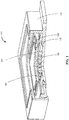
- an imaging device 100 such as a SWIR camera, sensor, short-wavelength infrared focal plane array, or any other imaging device
- the Focal Plane Array can refer to either the combination of a Photodiode Array (PDA) and Readout Integrated Circuit (ROIC) once wired together, or alternatively, the entire device shown in FIG. 1 as imaging device 100.
- the imaging device 100 may be contained within a housing 130, such as a nickel-cobalt ferrous alloy housing.
- a housing 130 such as a nickel-cobalt ferrous alloy housing.
- saturated and/or low pixels in the input image can be excluded.
- Histogram start and end points are determined, and a variable plateau is calculated depending upon the type of enhancement desired.
- the plateau may be varied along the histogram and can take on any desired shape, size, or number of plateau regions.
- the histogram is clipped.
- a cumulative histogram is constructed from the clipped histogram, and is normalized.
- the input image is then transformed into an enhanced output image using the normalized cumulative histogram as a look-up table.
- Optional non-linear operations can be performed on the normalized cumulative histogram.
- the enhancement method can be automatically varied to adapt to various imaging device types.
- the encapsulants disclosed herein may be positioned based on their ability to facilitate continued operation of the SWIR electronics.
- the encapsulant 105 may substantially cover the ROIC but not the PDA, so as to avoid optical interference. In this way, operation of the SWIR electronics 100 may remain unaffected.
- the epoxy encapsulant 105 may be chosen to be utilized with a SWIR focal plane array 150.
- an opaque epoxy encapsulant 105 is embedded with a high concentration of particles made of a material with a high radiopacity in the x-ray band.
- This high concentration of particles may substantially surround and cover a ROIC 125 and any associated electronics in an opto-electronic package 120, however, the encapsulant 105 may not cover the PDA to avoid optical interference.
- This concentration of high atomic number (e.g., Z) particles may be located in areas of interest proximate circuitry, such as integrated circuit (ROIC) 125 and associated electronics.
- the high radiopacity material (e.g., high concentration of particles made of a material with a high radiopacity in the x-ray band) may be selected to be transparent in a wavelength band of interest for operation of the SWIR electronics 100.
- the high radiopacity material is radio opaque to x-rays that may comprise a concentration of particles that have high radiopacity to x-rays.
- the encapsulant may comprise a radio blocking material that blocks x-rays through radiodensity.
- Radio opaque as used herein may refer to a relative inability of electromagnetic radiation, particularly X-rays, to pass through a particular material.
- the encapsulant 105 may be seeded with a class of compounds referred to as "monochromating crystals", which have been ground to a fine particle size.
- monochromating crystals Two examples of this class of compounds would be Lithium Fluoride (LiF) and Indium Antimonide (InSb). These compounds may reflect and/or refract X-rays at specific angles. Ground into a fine powder and embedded in the encapsulant, the compounds may be configured to cause X-rays used to inspect the device 100 to be reflected at random angles, further hindering attempts at reverse engineering.
- Embedding the epoxy encapsulant 105 with particles of a high-radiopacity material may be configured to hinder attempts at reverse engineering the structure of ROICs 125 by way of X-ray examination.
- the high-radiopacity materials may include materials commonly used in medical devices for absorption of X-rays, (e.g. Barium Sulfate, Bismuth Subcarbonate, Bismuth Oxychloride, and/or Tungsten Carbide).
- any epoxy encapsulant 105 compound containing high-Z (e.g., Z value greater than 50) elements may suffice. These high-Z elements may be any size, such as on the nanoparticle scale.
- a method currently in use for reverse-engineering electronics is to dissolve the epoxy encapsulant with a mixture of strong solvents and acids. This approach is limited to well-funded entities, as the equipment required to do this safely without destroying the device is costly.
- the chemical mixtures used in this process typically utilize nitric acid as one of its ingredients.
- a thin filament of wire embedded just below the surface of the encapsulant could be used as an "electronic tripwire" 160.
- the electronic tripwire 160 may be configured to both carry an electronic signal and dissolve in a solvent utilized to remove an epoxy encapsulant 105, such as nitric acid.
- the electronic tripwire 160 may render the associated circuitry, such as the circuitry associated with the integrated circuit (ROIC) 125 and associated electronics useless.
- ROIC integrated circuit
- a charge may be transmitted through the circuitry to render the ROIC 125 and associated electronics, such as an opto-electronics package 120, useless and/or inoperable.
- the electronic tripwire 160 may prevent a charge from being dissipated through a portion of the electronics; however, in response to being severed and/or dissolved, the charge may be released. In this way, the electronic tripwire 160 is coupled to a power supply, such as a capacitor and/or battery.
- the electronic tripwire 160 may be integral to the circuitry and utilized in normal operation of the device.
- the electronic tripwire 160 may be a non-traditional circuitry material capable of transmitting electric signals.
- These circuits integral to the operation of the electronics, such as SWIR electronics, made from "trip wire" materials, may dissolve with the dissolving of the encapsulant, rendering reverse engineering difficult and/or unlikely.
- the electronic tripwire 160 may be made from a material which is highly susceptible to attack by nitric acid. Stated another way, the electronic tripwire 160 may dissolve along with the epoxy encapsulant 105.
- the electronic tripwire 160 may be made from copper, silver, or nickel.
- the electronic tripwire 160 filament may be embedded proximate to and/or below the encapsulant 105 surface.
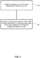
- An encapsulant may be embedded with high-radiopacity particulates or monochromating crystals (step 210). This embedded encapsulant may encase an electronic tripwire, which upon tripping and/or dissolving will substantially render the electronics inoperable and reduce susceptibility to reverse engineering (step 220).
Landscapes
- Engineering & Computer Science (AREA)
- Multimedia (AREA)
- Signal Processing (AREA)
- Physics & Mathematics (AREA)
- General Physics & Mathematics (AREA)
- Theoretical Computer Science (AREA)
- Semiconductor Integrated Circuits (AREA)
- Chemical & Material Sciences (AREA)
- Ceramic Engineering (AREA)
- Solid State Image Pick-Up Elements (AREA)
- Structures Or Materials For Encapsulating Or Coating Semiconductor Devices Or Solid State Devices (AREA)
Claims (14)
- Abbildungsgerät (100), umfassend:ein kurzwelliges Infrarot-Array im Brennfeld (150);einen integrierten Leseschaltkreis (125), der in einem Verkapselungsmaterial (105) eingekapselt ist, wobei das Verkapselungsmaterial in Teilchen mit hoher Strahlenundurchlässigkeit eingebettet ist; undeinen elektronischen Auslösedraht (160), der in dem Verkapselungsmaterial eingebettet ist und mit dem integrierten Leseschaltkreis verbunden ist, der konfiguriert ist, um den integrierten Leseschaltkreis als Reaktion darauf, dass der elektronische Auslösedraht durchtrennt wird, außer Funktion zu setzen.
- Abbildungsgerät nach Anspruch 1, wobei die Teilchen mit hoher Strahlenundurchlässigkeit eine Ordnungszahl (Z) über 50 umfassen.
- Abbildungsgerät nach Anspruch 1 oder 2, wobei der elektronische Auslösedraht mit einer Stromquelle verbunden ist.
- Abbildungsgerät nach Anspruch 1, 2 oder 3, wobei der elektronische Auslösedraht in den Betrieb des integrierten Leseschaltkreises während des normalen Betriebs des integrierten Leseschaltkreises integriert ist.
- Abbildungsgerät nach einem der vorstehenden Ansprüche, wobei die Teilchen mit hoher Strahlenundurchlässigkeit aus einer Gruppe ausgewählt sind, die Bariumsulfat, basisches Bismutcarbonat, Bismutoxychlorid und Wolframcarbid umfasst.
- Abbildungsgerät nach einem der vorstehenden Ansprüche, wobei das Verkapselungsmaterial in monochromatische Kristalle eingebettet ist.
- Abbildungsgerät nach einem der vorstehenden Ansprüche, wobei der elektronische Auslösedraht mindestens eines aus Kupfer, Silber oder Nickel ist.
- Abbildungsgerät nach einem der vorstehenden Ansprüche, wobei der elektronische Auslösedraht konfiguriert ist, um sich in einer Lösung aufzulösen, die konfiguriert ist, um das Verkapselungsmittel aufzulösen.
- Abbildungsgerät nach einem der vorstehenden Ansprüche, wobei der elektronische Auslösedraht konfiguriert ist, um elektronische Signale zu übertragen.
- Verkapselungsmaterial (105), umfassend:Teilchen mit hoher Strahlenundurchlässigkeit, die in das Verkapselungsmaterial eingebettet sind; undeinen elektronischen Auslösedraht (160), der in das Verkapselungsmaterial eingebettet ist, wobei der elektronische Auslösedraht mit einem integrierten Leseschaltkreis (125) eines kurzwelligen Infrarot-Arrays im Brennfeld (150) verbunden ist und konfiguriert ist, um den integrierten Leseschaltkreis als Reaktion darauf, dass der elektronische Auslösedraht durchtrennt wird, außer Funktion zu setzen; wobei der elektronische Auslösedraht mit einer Stromquelle verbunden ist und als Reaktion darauf, dass der Auslösedraht durchtrennt wird, eine Ladung von der Stromquelle freigesetzt wird, wodurch der integrierte Schaltkreis außer Funktion gesetzt wird.
- Verkapselungsmaterial nach Anspruch 10, wobei die Teilchen mit hoher Strahlenundurchlässigkeit einen Z-Wert über 50 aufweisen.
- Verkapselungsmaterial nach Anspruch 10 oder 11, wobei die Teilchen mit hoher Strahlenundurchlässigkeit aus einer Gruppe aus Bariumsulfat, basischem Bismutcarbonat, Bismutoxychlorid oder Wolframcarbid ausgewählt sind.
- Verkapselungsmaterial nach einem der Ansprüche 10 bis 12, wobei das Verkapselungsmaterial in monochromatische Kristalle eingebettet ist.
- Verkapselungsmaterial nach einem der Ansprüche 10 bis 13, wobei der elektronische Auslösedraht konfiguriert ist, um sich in einer Lösung aufzulösen, die konfiguriert ist, um das Verkapselungsmittel aufzulösen, wobei das Auflösen das Auslösen des elektronischen Auslösedrahts bewirkt.
Applications Claiming Priority (1)
| Application Number | Priority Date | Filing Date | Title |
|---|---|---|---|
| US14/638,808 US9756273B2 (en) | 2015-03-04 | 2015-03-04 | Multi-tiered tamper-resistant assembly system and method |
Publications (2)
| Publication Number | Publication Date |
|---|---|
| EP3065178A1 EP3065178A1 (de) | 2016-09-07 |
| EP3065178B1 true EP3065178B1 (de) | 2018-09-26 |
Family
ID=55587034
Family Applications (1)
| Application Number | Title | Priority Date | Filing Date |
|---|---|---|---|
| EP16158689.6A Not-in-force EP3065178B1 (de) | 2015-03-04 | 2016-03-04 | Mehrstufiges manipulationssicheres bestückungssystem |
Country Status (3)
| Country | Link |
|---|---|
| US (1) | US9756273B2 (de) |
| EP (1) | EP3065178B1 (de) |
| TW (1) | TW201637104A (de) |
Families Citing this family (2)
| Publication number | Priority date | Publication date | Assignee | Title |
|---|---|---|---|---|
| EP4047644A1 (de) * | 2021-02-23 | 2022-08-24 | Siemens Aktiengesellschaft | Elektronische baugruppe, füllmittel und verfahren zur qualitätsprüfung |
| US12087462B1 (en) | 2024-05-03 | 2024-09-10 | Honeywell Federal Manufacturing & Technologies, Llc | Radiopaque particle processing additive |
Family Cites Families (10)
| Publication number | Priority date | Publication date | Assignee | Title |
|---|---|---|---|---|
| US3424270A (en) * | 1965-05-12 | 1969-01-28 | Us Plywood Champ Papers Inc | Viscoelastic sound-blocking material with filler of high density particles |
| US3722977A (en) * | 1971-08-30 | 1973-03-27 | Beckman Instruments Inc | Optical scattering filter |
| US6417605B1 (en) * | 1994-09-16 | 2002-07-09 | Micron Technology, Inc. | Method of preventing junction leakage in field emission devices |
| US6879341B1 (en) * | 1997-07-15 | 2005-04-12 | Silverbrook Research Pty Ltd | Digital camera system containing a VLIW vector processor |
| US20110031982A1 (en) * | 2009-08-06 | 2011-02-10 | Irvine Sensors Corporation | Tamper-resistant electronic circuit and module incorporating electrically conductive nano-structures |
| US20140042322A1 (en) * | 2010-06-11 | 2014-02-13 | Chemimage Corporation | Portable System and Method for Detecting Drug Materials |
| US8809784B2 (en) * | 2010-10-21 | 2014-08-19 | Raytheon Company | Incident radiation detector packaging |
| JP2014528749A (ja) * | 2011-08-01 | 2014-10-30 | インフラレッド イメージング システムス,インク.InfraRed Imaging Systems, Inc. | 皮下組織の可視化を向上させるディスポーザブル光源 |
| US9000344B2 (en) * | 2013-03-15 | 2015-04-07 | Sensors Unlimited, Inc. | Focal plane array periphery through-vias for read out integrated circuit |
| US9087851B2 (en) * | 2013-05-22 | 2015-07-21 | International Business Machines Corporation | Silicon-based electronics with disabling feature |
-
2015
- 2015-03-04 US US14/638,808 patent/US9756273B2/en not_active Expired - Fee Related
- 2015-12-16 TW TW104142344A patent/TW201637104A/zh unknown
-
2016
- 2016-03-04 EP EP16158689.6A patent/EP3065178B1/de not_active Not-in-force
Non-Patent Citations (1)
| Title |
|---|
| None * |
Also Published As
| Publication number | Publication date |
|---|---|
| US20160261812A1 (en) | 2016-09-08 |
| TW201637104A (zh) | 2016-10-16 |
| EP3065178A1 (de) | 2016-09-07 |
| US9756273B2 (en) | 2017-09-05 |
Similar Documents
| Publication | Publication Date | Title |
|---|---|---|
| Wu et al. | Metal halide perovskites for X-ray detection and imaging | |
| Cao et al. | Shining emitter in a stable host: design of halide perovskite scintillators for X-ray imaging from commercial concept | |
| KR102004801B1 (ko) | 팬-아웃 반도체 패키지 | |
| US20090068474A1 (en) | Alkali silicate glass based coating and method for applying | |
| US20100213590A1 (en) | Systems and Methods of Tamper Proof Packaging of a Semiconductor Device | |
| KR20180032914A (ko) | 팬-아웃 센서 패키지 및 이를 포함하는 카메라 모듈 | |
| US9966409B2 (en) | Imaging device for electromagnetic radiation | |
| CN107112341A (zh) | 半导体装置和制造方法以及电子设备 | |
| EP3186833B1 (de) | Strahlungsdetektor | |
| US9756273B2 (en) | Multi-tiered tamper-resistant assembly system and method | |
| TW201635507A (zh) | 形成影像感測器積體電路封裝之方法 | |
| US20210202557A1 (en) | Radiation-resistant image sensor package | |
| WO2014196285A1 (ja) | 半導体装置 | |
| Sasajima et al. | New development trend of epoxy molding compound for encapsulating semiconductor chips | |
| US20200194341A1 (en) | Semiconductor Package and Fabricating Method thereof | |
| US9720107B2 (en) | Method and apparatus for differentially detecting beta rays and gamma rays included in radio active rays and package comprising the apparatus | |
| US10670743B2 (en) | Semiconductor detector and method for packaging the same | |
| JP6320517B2 (ja) | 耐放射線強化した超小型電子チップのパッケージング技術 | |
| TWI897996B (zh) | 攝像裝置及電子裝置 | |
| TWI252567B (en) | Package structure | |
| Keun Lee et al. | Thermal analysis of LED lamp with LTCC‐COB package | |
| US20190378815A1 (en) | Laser assisted solder bonding of direct conversion compound semiconductor detector | |
| Gedda et al. | Metal Halide Perovskites for High-Energy Radiation Detection | |
| EP3419050A1 (de) | Strahlungsgehärtetes gehäuse für eine elektronische vorrichtung und verfahren zur herstellung eines strahlungsgehärteten gehäuses | |
| Kim et al. | Novel decapsulation method for silver-based wire-bond semiconductor packages with high reliability using mixed salt–acid chemistry |
Legal Events
| Date | Code | Title | Description |
|---|---|---|---|
| PUAI | Public reference made under article 153(3) epc to a published international application that has entered the european phase |
Free format text: ORIGINAL CODE: 0009012 |
|
| AK | Designated contracting states |
Kind code of ref document: A1 Designated state(s): AL AT BE BG CH CY CZ DE DK EE ES FI FR GB GR HR HU IE IS IT LI LT LU LV MC MK MT NL NO PL PT RO RS SE SI SK SM TR |
|
| AX | Request for extension of the european patent |
Extension state: BA ME |
|
| STAA | Information on the status of an ep patent application or granted ep patent |
Free format text: STATUS: REQUEST FOR EXAMINATION WAS MADE |
|
| 17P | Request for examination filed |
Effective date: 20170307 |
|
| RBV | Designated contracting states (corrected) |
Designated state(s): AL AT BE BG CH CY CZ DE DK EE ES FI FR GB GR HR HU IE IS IT LI LT LU LV MC MK MT NL NO PL PT RO RS SE SI SK SM TR |
|
| GRAP | Despatch of communication of intention to grant a patent |
Free format text: ORIGINAL CODE: EPIDOSNIGR1 |
|
| STAA | Information on the status of an ep patent application or granted ep patent |
Free format text: STATUS: GRANT OF PATENT IS INTENDED |
|
| RIC1 | Information provided on ipc code assigned before grant |
Ipc: H01L 23/00 20060101ALI20180312BHEP Ipc: H01L 27/146 20060101AFI20180312BHEP Ipc: H01L 23/29 20060101ALI20180312BHEP |
|
| INTG | Intention to grant announced |
Effective date: 20180409 |
|
| GRAS | Grant fee paid |
Free format text: ORIGINAL CODE: EPIDOSNIGR3 |
|
| GRAA | (expected) grant |
Free format text: ORIGINAL CODE: 0009210 |
|
| STAA | Information on the status of an ep patent application or granted ep patent |
Free format text: STATUS: THE PATENT HAS BEEN GRANTED |
|
| AK | Designated contracting states |
Kind code of ref document: B1 Designated state(s): AL AT BE BG CH CY CZ DE DK EE ES FI FR GB GR HR HU IE IS IT LI LT LU LV MC MK MT NL NO PL PT RO RS SE SI SK SM TR |
|
| REG | Reference to a national code |
Ref country code: GB Ref legal event code: FG4D |
|
| REG | Reference to a national code |
Ref country code: CH Ref legal event code: EP |
|
| REG | Reference to a national code |
Ref country code: AT Ref legal event code: REF Ref document number: 1047037 Country of ref document: AT Kind code of ref document: T Effective date: 20181015 |
|
| REG | Reference to a national code |
Ref country code: IE Ref legal event code: FG4D |
|
| REG | Reference to a national code |
Ref country code: DE Ref legal event code: R096 Ref document number: 602016005838 Country of ref document: DE |
|
| REG | Reference to a national code |
Ref country code: NL Ref legal event code: MP Effective date: 20180926 |
|
| PG25 | Lapsed in a contracting state [announced via postgrant information from national office to epo] |
Ref country code: RS Free format text: LAPSE BECAUSE OF FAILURE TO SUBMIT A TRANSLATION OF THE DESCRIPTION OR TO PAY THE FEE WITHIN THE PRESCRIBED TIME-LIMIT Effective date: 20180926 Ref country code: LT Free format text: LAPSE BECAUSE OF FAILURE TO SUBMIT A TRANSLATION OF THE DESCRIPTION OR TO PAY THE FEE WITHIN THE PRESCRIBED TIME-LIMIT Effective date: 20180926 Ref country code: SE Free format text: LAPSE BECAUSE OF FAILURE TO SUBMIT A TRANSLATION OF THE DESCRIPTION OR TO PAY THE FEE WITHIN THE PRESCRIBED TIME-LIMIT Effective date: 20180926 Ref country code: BG Free format text: LAPSE BECAUSE OF FAILURE TO SUBMIT A TRANSLATION OF THE DESCRIPTION OR TO PAY THE FEE WITHIN THE PRESCRIBED TIME-LIMIT Effective date: 20181226 Ref country code: GR Free format text: LAPSE BECAUSE OF FAILURE TO SUBMIT A TRANSLATION OF THE DESCRIPTION OR TO PAY THE FEE WITHIN THE PRESCRIBED TIME-LIMIT Effective date: 20181227 Ref country code: FI Free format text: LAPSE BECAUSE OF FAILURE TO SUBMIT A TRANSLATION OF THE DESCRIPTION OR TO PAY THE FEE WITHIN THE PRESCRIBED TIME-LIMIT Effective date: 20180926 Ref country code: NO Free format text: LAPSE BECAUSE OF FAILURE TO SUBMIT A TRANSLATION OF THE DESCRIPTION OR TO PAY THE FEE WITHIN THE PRESCRIBED TIME-LIMIT Effective date: 20181226 |
|
| REG | Reference to a national code |
Ref country code: LT Ref legal event code: MG4D |
|
| PG25 | Lapsed in a contracting state [announced via postgrant information from national office to epo] |
Ref country code: HR Free format text: LAPSE BECAUSE OF FAILURE TO SUBMIT A TRANSLATION OF THE DESCRIPTION OR TO PAY THE FEE WITHIN THE PRESCRIBED TIME-LIMIT Effective date: 20180926 Ref country code: LV Free format text: LAPSE BECAUSE OF FAILURE TO SUBMIT A TRANSLATION OF THE DESCRIPTION OR TO PAY THE FEE WITHIN THE PRESCRIBED TIME-LIMIT Effective date: 20180926 Ref country code: AL Free format text: LAPSE BECAUSE OF FAILURE TO SUBMIT A TRANSLATION OF THE DESCRIPTION OR TO PAY THE FEE WITHIN THE PRESCRIBED TIME-LIMIT Effective date: 20180926 |
|
| REG | Reference to a national code |
Ref country code: AT Ref legal event code: MK05 Ref document number: 1047037 Country of ref document: AT Kind code of ref document: T Effective date: 20180926 |
|
| PG25 | Lapsed in a contracting state [announced via postgrant information from national office to epo] |
Ref country code: IT Free format text: LAPSE BECAUSE OF FAILURE TO SUBMIT A TRANSLATION OF THE DESCRIPTION OR TO PAY THE FEE WITHIN THE PRESCRIBED TIME-LIMIT Effective date: 20180926 Ref country code: RO Free format text: LAPSE BECAUSE OF FAILURE TO SUBMIT A TRANSLATION OF THE DESCRIPTION OR TO PAY THE FEE WITHIN THE PRESCRIBED TIME-LIMIT Effective date: 20180926 Ref country code: CZ Free format text: LAPSE BECAUSE OF FAILURE TO SUBMIT A TRANSLATION OF THE DESCRIPTION OR TO PAY THE FEE WITHIN THE PRESCRIBED TIME-LIMIT Effective date: 20180926 Ref country code: EE Free format text: LAPSE BECAUSE OF FAILURE TO SUBMIT A TRANSLATION OF THE DESCRIPTION OR TO PAY THE FEE WITHIN THE PRESCRIBED TIME-LIMIT Effective date: 20180926 Ref country code: AT Free format text: LAPSE BECAUSE OF FAILURE TO SUBMIT A TRANSLATION OF THE DESCRIPTION OR TO PAY THE FEE WITHIN THE PRESCRIBED TIME-LIMIT Effective date: 20180926 Ref country code: ES Free format text: LAPSE BECAUSE OF FAILURE TO SUBMIT A TRANSLATION OF THE DESCRIPTION OR TO PAY THE FEE WITHIN THE PRESCRIBED TIME-LIMIT Effective date: 20180926 Ref country code: NL Free format text: LAPSE BECAUSE OF FAILURE TO SUBMIT A TRANSLATION OF THE DESCRIPTION OR TO PAY THE FEE WITHIN THE PRESCRIBED TIME-LIMIT Effective date: 20180926 Ref country code: PL Free format text: LAPSE BECAUSE OF FAILURE TO SUBMIT A TRANSLATION OF THE DESCRIPTION OR TO PAY THE FEE WITHIN THE PRESCRIBED TIME-LIMIT Effective date: 20180926 Ref country code: IS Free format text: LAPSE BECAUSE OF FAILURE TO SUBMIT A TRANSLATION OF THE DESCRIPTION OR TO PAY THE FEE WITHIN THE PRESCRIBED TIME-LIMIT Effective date: 20190126 |
|
| PGFP | Annual fee paid to national office [announced via postgrant information from national office to epo] |
Ref country code: DE Payment date: 20190219 Year of fee payment: 4 |
|
| PG25 | Lapsed in a contracting state [announced via postgrant information from national office to epo] |
Ref country code: SK Free format text: LAPSE BECAUSE OF FAILURE TO SUBMIT A TRANSLATION OF THE DESCRIPTION OR TO PAY THE FEE WITHIN THE PRESCRIBED TIME-LIMIT Effective date: 20180926 Ref country code: PT Free format text: LAPSE BECAUSE OF FAILURE TO SUBMIT A TRANSLATION OF THE DESCRIPTION OR TO PAY THE FEE WITHIN THE PRESCRIBED TIME-LIMIT Effective date: 20190126 Ref country code: SM Free format text: LAPSE BECAUSE OF FAILURE TO SUBMIT A TRANSLATION OF THE DESCRIPTION OR TO PAY THE FEE WITHIN THE PRESCRIBED TIME-LIMIT Effective date: 20180926 |
|
| PGFP | Annual fee paid to national office [announced via postgrant information from national office to epo] |
Ref country code: BE Payment date: 20190222 Year of fee payment: 4 |
|
| REG | Reference to a national code |
Ref country code: DE Ref legal event code: R097 Ref document number: 602016005838 Country of ref document: DE |
|
| PG25 | Lapsed in a contracting state [announced via postgrant information from national office to epo] |
Ref country code: DK Free format text: LAPSE BECAUSE OF FAILURE TO SUBMIT A TRANSLATION OF THE DESCRIPTION OR TO PAY THE FEE WITHIN THE PRESCRIBED TIME-LIMIT Effective date: 20180926 |
|
| PLBE | No opposition filed within time limit |
Free format text: ORIGINAL CODE: 0009261 |
|
| STAA | Information on the status of an ep patent application or granted ep patent |
Free format text: STATUS: NO OPPOSITION FILED WITHIN TIME LIMIT |
|
| 26N | No opposition filed |
Effective date: 20190627 |
|
| PG25 | Lapsed in a contracting state [announced via postgrant information from national office to epo] |
Ref country code: MC Free format text: LAPSE BECAUSE OF FAILURE TO SUBMIT A TRANSLATION OF THE DESCRIPTION OR TO PAY THE FEE WITHIN THE PRESCRIBED TIME-LIMIT Effective date: 20180926 Ref country code: SI Free format text: LAPSE BECAUSE OF FAILURE TO SUBMIT A TRANSLATION OF THE DESCRIPTION OR TO PAY THE FEE WITHIN THE PRESCRIBED TIME-LIMIT Effective date: 20180926 |
|
| REG | Reference to a national code |
Ref country code: CH Ref legal event code: PL |
|
| PG25 | Lapsed in a contracting state [announced via postgrant information from national office to epo] |
Ref country code: LU Free format text: LAPSE BECAUSE OF NON-PAYMENT OF DUE FEES Effective date: 20190304 |
|
| PG25 | Lapsed in a contracting state [announced via postgrant information from national office to epo] |
Ref country code: LI Free format text: LAPSE BECAUSE OF NON-PAYMENT OF DUE FEES Effective date: 20190331 Ref country code: IE Free format text: LAPSE BECAUSE OF NON-PAYMENT OF DUE FEES Effective date: 20190304 Ref country code: CH Free format text: LAPSE BECAUSE OF NON-PAYMENT OF DUE FEES Effective date: 20190331 |
|
| PG25 | Lapsed in a contracting state [announced via postgrant information from national office to epo] |
Ref country code: FR Free format text: LAPSE BECAUSE OF NON-PAYMENT OF DUE FEES Effective date: 20190331 |
|
| PG25 | Lapsed in a contracting state [announced via postgrant information from national office to epo] |
Ref country code: TR Free format text: LAPSE BECAUSE OF FAILURE TO SUBMIT A TRANSLATION OF THE DESCRIPTION OR TO PAY THE FEE WITHIN THE PRESCRIBED TIME-LIMIT Effective date: 20180926 |
|
| PG25 | Lapsed in a contracting state [announced via postgrant information from national office to epo] |
Ref country code: MT Free format text: LAPSE BECAUSE OF NON-PAYMENT OF DUE FEES Effective date: 20190304 |
|
| REG | Reference to a national code |
Ref country code: DE Ref legal event code: R119 Ref document number: 602016005838 Country of ref document: DE |
|
| REG | Reference to a national code |
Ref country code: BE Ref legal event code: MM Effective date: 20200331 |
|
| PG25 | Lapsed in a contracting state [announced via postgrant information from national office to epo] |
Ref country code: DE Free format text: LAPSE BECAUSE OF NON-PAYMENT OF DUE FEES Effective date: 20201001 |
|
| PG25 | Lapsed in a contracting state [announced via postgrant information from national office to epo] |
Ref country code: BE Free format text: LAPSE BECAUSE OF NON-PAYMENT OF DUE FEES Effective date: 20200331 |
|
| GBPC | Gb: european patent ceased through non-payment of renewal fee |
Effective date: 20200304 |
|
| PG25 | Lapsed in a contracting state [announced via postgrant information from national office to epo] |
Ref country code: GB Free format text: LAPSE BECAUSE OF NON-PAYMENT OF DUE FEES Effective date: 20200304 |
|
| PG25 | Lapsed in a contracting state [announced via postgrant information from national office to epo] |
Ref country code: CY Free format text: LAPSE BECAUSE OF FAILURE TO SUBMIT A TRANSLATION OF THE DESCRIPTION OR TO PAY THE FEE WITHIN THE PRESCRIBED TIME-LIMIT Effective date: 20180926 |
|
| PG25 | Lapsed in a contracting state [announced via postgrant information from national office to epo] |
Ref country code: HU Free format text: LAPSE BECAUSE OF FAILURE TO SUBMIT A TRANSLATION OF THE DESCRIPTION OR TO PAY THE FEE WITHIN THE PRESCRIBED TIME-LIMIT; INVALID AB INITIO Effective date: 20160304 |
|
| PG25 | Lapsed in a contracting state [announced via postgrant information from national office to epo] |
Ref country code: MK Free format text: LAPSE BECAUSE OF FAILURE TO SUBMIT A TRANSLATION OF THE DESCRIPTION OR TO PAY THE FEE WITHIN THE PRESCRIBED TIME-LIMIT Effective date: 20180926 |