EP3065167A1 - High-frequency module and microwave transceiver - Google Patents
High-frequency module and microwave transceiver Download PDFInfo
- Publication number
- EP3065167A1 EP3065167A1 EP15202391.7A EP15202391A EP3065167A1 EP 3065167 A1 EP3065167 A1 EP 3065167A1 EP 15202391 A EP15202391 A EP 15202391A EP 3065167 A1 EP3065167 A1 EP 3065167A1
- Authority
- EP
- European Patent Office
- Prior art keywords
- microwave
- wiring board
- board
- multilayer wiring
- metal core
- Prior art date
- Legal status (The legal status is an assumption and is not a legal conclusion. Google has not performed a legal analysis and makes no representation as to the accuracy of the status listed.)
- Granted
Links
Images



Classifications
-
- H—ELECTRICITY
- H04—ELECTRIC COMMUNICATION TECHNIQUE
- H04B—TRANSMISSION
- H04B1/00—Details of transmission systems, not covered by a single one of groups H04B3/00 - H04B13/00; Details of transmission systems not characterised by the medium used for transmission
- H04B1/02—Transmitters
- H04B1/03—Constructional details, e.g. casings, housings
- H04B1/036—Cooling arrangements
-
- H—ELECTRICITY
- H10—SEMICONDUCTOR DEVICES; ELECTRIC SOLID-STATE DEVICES NOT OTHERWISE PROVIDED FOR
- H10W—GENERIC PACKAGES, INTERCONNECTIONS, CONNECTORS OR OTHER CONSTRUCTIONAL DETAILS OF DEVICES COVERED BY CLASS H10
- H10W40/00—Arrangements for thermal protection or thermal control
- H10W40/20—Arrangements for cooling
- H10W40/22—Arrangements for cooling characterised by their shape, e.g. having conical or cylindrical projections
-
- H—ELECTRICITY
- H10—SEMICONDUCTOR DEVICES; ELECTRIC SOLID-STATE DEVICES NOT OTHERWISE PROVIDED FOR
- H10W—GENERIC PACKAGES, INTERCONNECTIONS, CONNECTORS OR OTHER CONSTRUCTIONAL DETAILS OF DEVICES COVERED BY CLASS H10
- H10W40/00—Arrangements for thermal protection or thermal control
- H10W40/20—Arrangements for cooling
- H10W40/22—Arrangements for cooling characterised by their shape, e.g. having conical or cylindrical projections
- H10W40/226—Arrangements for cooling characterised by their shape, e.g. having conical or cylindrical projections characterised by projecting parts, e.g. fins to increase surface area
- H10W40/228—Arrangements for cooling characterised by their shape, e.g. having conical or cylindrical projections characterised by projecting parts, e.g. fins to increase surface area the projecting parts being wire-shaped or pin-shaped
-
- H—ELECTRICITY
- H10—SEMICONDUCTOR DEVICES; ELECTRIC SOLID-STATE DEVICES NOT OTHERWISE PROVIDED FOR
- H10W—GENERIC PACKAGES, INTERCONNECTIONS, CONNECTORS OR OTHER CONSTRUCTIONAL DETAILS OF DEVICES COVERED BY CLASS H10
- H10W42/00—Arrangements for protection of devices
- H10W42/20—Arrangements for protection of devices protecting against electromagnetic or particle radiation, e.g. light, X-rays, gamma-rays or electrons
-
- H—ELECTRICITY
- H10—SEMICONDUCTOR DEVICES; ELECTRIC SOLID-STATE DEVICES NOT OTHERWISE PROVIDED FOR
- H10W—GENERIC PACKAGES, INTERCONNECTIONS, CONNECTORS OR OTHER CONSTRUCTIONAL DETAILS OF DEVICES COVERED BY CLASS H10
- H10W44/00—Electrical arrangements for controlling or matching impedance
- H10W44/20—Electrical arrangements for controlling or matching impedance at high-frequency [HF] or radio frequency [RF]
-
- H—ELECTRICITY
- H10—SEMICONDUCTOR DEVICES; ELECTRIC SOLID-STATE DEVICES NOT OTHERWISE PROVIDED FOR
- H10W—GENERIC PACKAGES, INTERCONNECTIONS, CONNECTORS OR OTHER CONSTRUCTIONAL DETAILS OF DEVICES COVERED BY CLASS H10
- H10W70/00—Package substrates; Interposers; Redistribution layers [RDL]
- H10W70/60—Insulating or insulated package substrates; Interposers; Redistribution layers
- H10W70/67—Insulating or insulated package substrates; Interposers; Redistribution layers characterised by their insulating layers or insulating parts
- H10W70/68—Shapes or dispositions thereof
- H10W70/6875—Shapes or dispositions thereof being on a metallic substrate, e.g. insulated metal substrates [IMS]
-
- H—ELECTRICITY
- H10—SEMICONDUCTOR DEVICES; ELECTRIC SOLID-STATE DEVICES NOT OTHERWISE PROVIDED FOR
- H10W—GENERIC PACKAGES, INTERCONNECTIONS, CONNECTORS OR OTHER CONSTRUCTIONAL DETAILS OF DEVICES COVERED BY CLASS H10
- H10W76/00—Containers; Fillings or auxiliary members therefor; Seals
- H10W76/10—Containers or parts thereof
- H10W76/12—Containers or parts thereof characterised by their shape
- H10W76/15—Containers comprising an insulating or insulated base
- H10W76/157—Containers comprising an insulating or insulated base having interconnections parallel to the insulating or insulated base
-
- H—ELECTRICITY
- H10—SEMICONDUCTOR DEVICES; ELECTRIC SOLID-STATE DEVICES NOT OTHERWISE PROVIDED FOR
- H10W—GENERIC PACKAGES, INTERCONNECTIONS, CONNECTORS OR OTHER CONSTRUCTIONAL DETAILS OF DEVICES COVERED BY CLASS H10
- H10W40/00—Arrangements for thermal protection or thermal control
- H10W40/60—Securing means for detachable heating or cooling arrangements, e.g. clamps
- H10W40/611—Bolts or screws
-
- H—ELECTRICITY
- H10—SEMICONDUCTOR DEVICES; ELECTRIC SOLID-STATE DEVICES NOT OTHERWISE PROVIDED FOR
- H10W—GENERIC PACKAGES, INTERCONNECTIONS, CONNECTORS OR OTHER CONSTRUCTIONAL DETAILS OF DEVICES COVERED BY CLASS H10
- H10W44/00—Electrical arrangements for controlling or matching impedance
- H10W44/20—Electrical arrangements for controlling or matching impedance at high-frequency [HF] or radio frequency [RF]
- H10W44/203—Electrical connections
- H10W44/216—Waveguides, e.g. strip lines
-
- H—ELECTRICITY
- H10—SEMICONDUCTOR DEVICES; ELECTRIC SOLID-STATE DEVICES NOT OTHERWISE PROVIDED FOR
- H10W—GENERIC PACKAGES, INTERCONNECTIONS, CONNECTORS OR OTHER CONSTRUCTIONAL DETAILS OF DEVICES COVERED BY CLASS H10
- H10W44/00—Electrical arrangements for controlling or matching impedance
- H10W44/20—Electrical arrangements for controlling or matching impedance at high-frequency [HF] or radio frequency [RF]
- H10W44/226—Electrical arrangements for controlling or matching impedance at high-frequency [HF] or radio frequency [RF] for HF amplifiers
Definitions
- Embodiments of the present disclosure relate to a high-frequency module and a microwave transceiver.
- Measures to efficiently dissipate heat generated by a power amplifier are taken in a wiring board on which the power amplifier is mounted.
- heat from the power amplifier is transferred to a heat sink provided on the wiring board via through-holes and conductor patterns.
- the heat sink dissipates the transferred heat to the exterior.
- each through-hole does not have a sufficient heat transfer performance, and the dimension of the heat sink has a restriction.
- GaN gallium nitride
- conventional microwave transceivers are constructed by a combination of a metal plate, a casing which will be a heat spreader, and a monolayer board or a multilayer board.
- Conventional microwave transceivers have disadvantages in at least any one of a high-frequency performance (discontinuity of grounding), a reliability (a deterioration of joined portions due to a difference of thermal expansion rate of components), an electromagnetic compatibility, and a price.
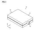
- FIG. 1 is a perspective view of a high-frequency module
- a high-frequency module includes a first board in which an opening is formed, and which includes a transmission circuit formed on a surface at a first side, the transmission circuit transmits a microwave, a first device disposed in the opening of the first board, a second board which is disposed at a second side of the first board which is formed with a control circuit for the first device, and in which an opening is formed at a location overlapping the first device, a metal core which is disposed between the first board and the second board, and which is in contact with the first device, and a casing which is formed of a metal, and which includes a connection connected with the metal core via the opening of the second board.
- FIG. 1 is a perspective view of a high-frequency module 10 according to this embodiment.
- the high-frequency module 10 is a device that amplifies, for example, microwave signals.
- the high-frequency module 10 is connected with, for example, a device for signal processing or communication and an antenna via connectors 12 provided on a module main unit 11.
- FIG. 2 is an exploded perspective view of the module main unit 11. As illustrated in FIG. 2 , the module main unit 11 includes a casing 20, a wiring board 50, and a cover 30.
- the casing 20 is, for example, a metal casing formed of a metal like aluminum which has a high electrical conductivity and which also has a high thermal conductivity.
- This casing 20 includes a bottom 22, a frame 21 formed along the outer edge of the bottom 22, and a protrusion 23 provided at the center of the bottom 22.
- the protrusion 23 protrudes upwardly from the upper face of the bottom 22.
- the cover 30 is formed of a metal like aluminum that has a high electrical conductivity like the casing 20, and includes a top panel, and a frame formed along the outer edge of the top plate.
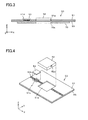
- FIG. 3 is a cross-sectional view of the wiring board 50.
- the wiring board 50 includes a metal core 55, a microwave propagation multilayer wiring board 51 disposed on the upper face of the metal core 55, and a multilayer wiring board 70 for a timing control logic circuit and an energy storage and regulation circuit disposed on the lower face of the metal core 55.
- the metal core 55 is, for example, formed of copper or aluminum that has a high thermal conductivity, and has a thickness of substantially 0.5 mm.
- the microwave propagation multilayer wiring board 51 is a board mainly consisting of, for example, an epoxy resin or a fluorine resin, and has a lower face bonded to the metal core 55.
- a cavity 51a is formed at the center part of the microwave propagation multilayer wiring board 51.
- the upper face of the metal core 55 is exposed via this cavity 51a.
- a pad 51c where the microwave active device 53 is to be mounted is formed at a -X side of the cavity 51 a. As illustrated in FIG. 3 , the pad 51 c is electrically connected with the metal core 55 via multiple thermal through-holes 51d provided in the microwave propagation multilayer wiring board 51.
- the thermal through-hole 51 d is a through hole which has a thermal resistance reduced and which has a thermal conductivity enhanced.
- This thermal through-hole 51 d is formed by forming a through-hole in the microwave propagation multilayer wiring board 51, and applying a copper plating to the internal wall of this through-hole so as to have a thick plating thickness.
- the thermal through-hole 51d may be formed by filling a conductive paste with an excellent thermal conductivity into the through-hole that has the internal wall to which copper plating is applied.
- the thermal through-hole 51d may be formed by filling a conductive paste in the through-hole without applying a copper plating. Note that in order to form the pad 51 c appropriate for the surface mounting, a cover plating is applied on the thermal through holes 51 d.
- a microwave transmission path 51b which runs through the center of the microwave propagation multilayer wiring board 51, and which reaches the +X-side end of the microwave propagation multilayer wiring board 51 from the -X-side end thereof is formed on the upper face of the microwave propagation multilayer wiring board 51.
- the microwave transmission path 51b includes three portions: a transmission path that reaches a nearby region of the pad 51c from the -X-side end of the microwave propagation multilayer wiring board 51; a transmission path that reaches the cavity 51a from the nearby region of the pad 51c; and a transmission path that reaches the +X-side end of the microwave propagation multilayer wiring board 51 from the cavity 51a.
- a microwave passive device such as a filter or a directional coupler, is formed on the microwave propagation multilayer wiring board 51.
- the multilayer wiring board 70 is a multilayer wiring board on which control circuits and power circuits for the microwave high-output power amplifier 52 and the microwave active device 53 are formed.
- the control circuits and the power circuits are each formed by conductor patterns formed on the multilayer wiring board 70, and electronic components mounted (reflow mounting) on the multilayer wiring board 70.
- a cavity 70a is formed in the multilayer wiring board 70.
- the multilayer wiring board 70 is bonded to the lower face of the metal core 55 via, for example, prepreg with the cavity 70a being positioned so as to overlap the cavity 51 a of the microwave propagation multilayer wiring board 51.
- the lower face of the metal core 55 is exposed via the cavity 70a of the multilayer wiring board 70.
- the microwave high-output power amplifier 52 and the microwave active device 53 are mounted on the wiring board 50.
- the microwave high-output power amplifier 52 is an amplifier to amplify a microwave signal transmitted through the microwave transmission path 51b. As illustrated in FIG. 4 , electrodes 52a are formed on a surface of the microwave high-output power amplifier 52 at the +X side, and a surface thereof at the -X side.
- the microwave high-output power amplifier 52 is bonded to the upper face of the metal core 55 via the cavity 51a of the microwave propagation multilayer wiring board 51 by, for example, a solder or an electrically-conductive adhesive.
- the respective electrodes 52a provided on the microwave high-output power amplifier 52 are connected with the microwave transmission path 51b by electrodes 60 as illustrated in FIG. 2 .
- the connection structure is not limited to this structure.
- the other electrodes of the microwave high-output power amplifier 52 are connected with the conductive layers of the multilayer wiring board 70 via through-hole conductors insulated from the metal core 55.
- the control circuit formed on the multilayer wiring board 70 is enabled to apply power to the microwave high-output power amplifier 52 and to control such a power application.
- the microwave active device 53 is, for example, a phase shifter, a switch, an attenuator, a buffer amplifier, a limiter, a low-noise amplifier, or a package of those elements.
- a rectangular heat dissipation pad 53a is formed on the lower face (a surface at the -Z side) of the microwave active device 53.
- electrode pads 53b to be connected with the microwave transmission path 51b are formed at the +X side and -X side of the heat dissipation pad 53a
- electrode pads 53c to be mainly connected with the multilayer wiring board 70 are formed at the +Y side and -Y side of the heat dissipation pad 53a.
- the microwave active device 53 is mounted on the microwave propagation multilayer wiring board 51.
- the heat dissipation pad 53a is connected with a pad 51c formed on the microwave propagation multilayer wiring board 51 by a solder, etc.
- the electrode pad 53b is connected with the microwave transmission path 51b. It is not illustrated in the figure but the electrode pad 53c is connected with a circuit formed on the multilayer wiring board 70 via an unillustrated through-hole conductor electrically insulated from the metal core 55. This enables the control circuit formed on the multilayer wiring board 70 to apply power to the microwave active device 53 and to control such a power application.
- FIG. 6 is an XZ cross-sectional view of the high-frequency module 10.
- the above-explained wiring board 50 is mounted on the casing 20.
- the protrusion 23 of the casing 20 is bonded to the metal core 55 by a solder, an electrically-conductive adhesive, etc., via the cavity 70a of the multilayer wiring board 70.
- the cover 30 is fastened to the casing 20 by, for example, screws via the wiring board 50.
- the casing 20, the cover 30, and the wiring board 50 are integrated one another, and thus the module main unit 11 is formed.
- a connector 12 to be connected with the microwave transmission path 51b is attached to this module main unit 11. Accordingly, the high-frequency module 10 is accomplished.
- the microwave high-output power amplifier 52 that has a large output is intimately in contact with the metal core 55 formed of a metal with a high thermal conductivity.
- the metal core 55 has a portion which is intimately in contact with the microwave high-output power amplifier 52 and which is also intimately in contact with the protrusion 23 of the casing 20 that serves as a heat sink.
- a thermal resistance between the microwave high-output power amplifier 52 and the casing 20 is reduced. Therefore, heat generated from the microwave high-output power amplifier 52 is efficiently transferred to the casing 20, and the casing 20 is capable of efficiently dissipating heat as the heat sink.
- the temperature rise of the microwave high-output power amplifier 52 is suppressible, and the performance stability and operation stability of the high-frequency module 10 are improved.
- a deterioration of the microwave high-output power amplifier 52 due to overheating is suppressed, thereby extending the life of the device.
- the microwave active device 53 is connected with the metal core 51d via the multiple thermal through-holes 51 d to which, for example, plating is applied.
- heat generated from the microwave active device 53 is transmitted to the casing 20 via the metal core 55, and then the casing 20 is capable of efficiently dissipating heat as the heat sink. Consequently, the temperature rise of the microwave active device 53 is suppressible, and the performance stability and operation stability of the high-frequency module 10 are improved.
- a deterioration of the microwave active device 53 due to overheating is suppressed, thereby extending the life of the device.
- the metal core 55 formed of a metal is disposed between the microwave propagation multilayer wiring board 51 on which the microwave transmission path 51b is formed, and, the multilayer wiring board 70 on which the control circuits are formed.
- the metal core 55 functions as a shield, and thus the microwave propagation multilayer wiring board 51 and the multilayer wiring board 70 are electromagnetically shielded against each other. Therefore, the performance stability and the operation stability are improved without causing a false operation of the high-frequency module 10 and an abnormal operation thereof.
- the reference potential of the wiring board 50 becomes the potential of the metal core 55.
- the microwave transmission path 51b has no discontinuous contact for grounding. Therefore, the microwave is transmittable without any performance deterioration.
- microwave transceivers include, for example, a metal plate and a casing that serve as a heat spreader, and various types of boards. According to such a type of microwave transceivers, various problems are involved, such as a high-frequency performance (grounding discontinuity), a reliability in accordance with an adverse effect to a joined portion due to thermal expansions of portions with different linear expansion coefficients, an electromagnetic wave interference, and prices.
- the microwave transceiver according to this embodiment has no discontinuous contact in the microwave transmission path, and has a relatively small number of components connected in series with the microwave transmission path. Therefore, the improved microwave transceiver of this embodiment is capable of addressing those problems.
- the microwave propagation multilayer wiring board 51 and the metal core 55 may be formed by a copper clad laminate 500 that includes an insulation resin layer 510, a copper foil 510b bonded to the upper face of the insulation resin layer 510, and a metal layer 550 which is bonded to the lower face of the insulation resin layer 510.
- the copper foil 510b on the upper face of the insulation resin layer 510 having undergone patterning constructs a microwave transmission path 51b, a pad 51c, etc., of the microwave propagation multilayer wiring board 51.
- the metal layer 550 on the lower face of the insulation resin layer 510 constructs the metal core 55.
- the copper foil 510b that becomes the pad 51c is electrically connected with the metal layer 550 via thermal through-holes 51d formed in the insulation resin layer 510.
- the copper clad laminate 500 and the multilayer wiring board 70 are bonded with each other via, for example, a prepreg 800. Hence, as illustrated in FIG. 8 , the copper clad laminate 500 and the multilayer wiring board 70 are integrated with each other.
- a cavity 51a present in the copper foil 510b and the insulation resin layer 510 is formed in the copper clad laminate 500, and the cavity 70a is formed in the multilayer wiring board 70 by, for example, laser beam. Accordingly, the wiring board 50 is accomplished.
- the microwave propagation multilayer wiring board 51 and the metal core 55 are formed of the copper clad laminate 500.
- the present disclosure is not limited to this structure, and for example, as is clear from FIG. 10 , only the microwave propagation multilayer wiring board 51 may be formed by the copper clad laminate 500 that includes the insulation resin layer 510, the copper foil 510b bonded to the upper face of the insulation resin layer 510, and a copper foil 510a bonded to the lower face of the insulation resin layer 510.
- the metal core 55 is bonded to the lower face of the copper clad laminate 500 by, for example, an electrically-conductive adhesive. Hence, the copper clad laminate 500 and the metal core 55 are integrated with each other.
- the metal core 55 and the multilayer wiring board 70 are bonded with each other via the prepreg 800. Accordingly, the copper clad laminate 500, the metal core 55, and the multilayer wiring board 70 are integrated one another. In addition, the cavity 51a present in the copper foil 510b and the insulation resin layer 510 is formed, and the cavity 70a is formed in the multilayer wiring board 70 is formed. Therefore, the wiring board 50 is accomplished.
- connection between the microwave propagation multilayer wiring board 51 and the multilayer wiring board 70 is realized by the through-hole conductors 51d as illustrated in FIGS. 6 , 7 , and 10 , etc. Hence, a labor work for connecting the microwave propagation multilayer wiring board 51 and the multilayer wiring board 70 is unnecessary, reducing the price of the product.
- the present disclosure is not limited to the aforementioned embodiment.
- the explanation was given of an example case in which the microwave active device 53 is mounted on the surface of the microwave propagation multilayer wiring board 51.
- the microwave propagation multilayer wiring board 51 may employ a multilayer structure, and the microwave active device 53 may be embedded and mounted inside the microwave propagation multilayer wiring board 51.
- the pad 51c on which the microwave active device 53 is mounted may be formed by an upper face of a metal member 51 e that is in a columnar or cuboid shape like a copper inlay.
- the pad 51 c is accomplished.
- the microwave high-output power amplifier 52 is bonded to the metal core 55.
- the microwave high-output power amplifier 52 may be fastened to the protrusion 23 of the casing 20 by screws 120.
- the screws 120 cause the microwave high-output power amplifier 52, the metal core 55, and the casing 20 to be intimately in contact with each other.
- heat from the microwave high-output power amplifier 52 is efficiently dissipated from the casing 20 that serves as a heat sink.
- the explanation was given of an example case in which the single microwave active device 53 is mounted on the microwave propagation multilayer wiring board 51.
- the present disclosure is not limited to this structure, and multiple microwave active devices 53 may be mounted on the microwave propagation multilayer wiring board 51.
- the high-frequency module 10 constructs a microwave transceiver 200 when connected with a radiator 91 like a printed dipole antenna element, and a device 92 for signal processing or communication.
- the high-frequency module 10 is packaged by the casing 20 and the cover 30. This facilitates a construction of a transceiver system that includes the multiple microwave transceivers 200.
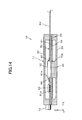
- a microwave wiring board 93 of the device 92 may be directly connected with the microwave propagation multilayer wiring board 51.
- the microwave wiring board 93 of the device 92 is mounted on the metal core 55 in a manner intimately contacting therewith.
- a grounding (GND) potential reference is unified for the high-frequency module 10 of this embodiment and the other device 92, thereby accomplishing a structure that has no discontinuous contact between the microwave propagation multilayer wiring board 51 and the microwave wiring board 93.
Landscapes
- Engineering & Computer Science (AREA)
- Computer Networks & Wireless Communication (AREA)
- Signal Processing (AREA)
- Production Of Multi-Layered Print Wiring Board (AREA)
- Cooling Or The Like Of Semiconductors Or Solid State Devices (AREA)
- Structure Of Printed Boards (AREA)
- Cooling Or The Like Of Electrical Apparatus (AREA)
- Insulated Metal Substrates For Printed Circuits (AREA)
- Transceivers (AREA)
- Physics & Mathematics (AREA)
- Health & Medical Sciences (AREA)
- Electromagnetism (AREA)
- Toxicology (AREA)
Abstract
Description
- Embodiments of the present disclosure relate to a high-frequency module and a microwave transceiver.
- In recent years, in accordance with the improvement of high functionality and multi-functionality of semiconductor devices, and of an operation speed thereof, the amount of heat generated by such semiconductor devices tends to increase. Hence, in the case of a multilayer wiring board that includes an insulation layer containing, for example, normal glass woven cloth or glass non-woven cloth, it is difficult to efficiently treat heat generated by a high-output power amplifier. In addition, according to this multilayer wiring board, an electromagnetic shielding effect, and an electromagnetic interference shielding effect are not expectable, and thus it is difficult to suppress an electromagnetic interference by shielding electromagnetic waves.
- Measures to efficiently dissipate heat generated by a power amplifier are taken in a wiring board on which the power amplifier is mounted. According to conventional wiring boards, heat from the power amplifier is transferred to a heat sink provided on the wiring board via through-holes and conductor patterns. The heat sink dissipates the transferred heat to the exterior.
- However, each through-hole does not have a sufficient heat transfer performance, and the dimension of the heat sink has a restriction. Hence, according to conventional technologies, it is difficult to mount a power amplifier that has a relatively large amount of heat generation per a unit area on the wiring board.
- In addition, in recent years, researches and developments are enhanced to improve a transmission output by applying a gallium nitride (GaN) transistor for the power amplifier so as not to increase the dimension of a microwave transceiver. Since the GaN transistor has a large output, a total amount of heat generation and an amount of heat generation per a unit area are relatively large. Conversely, when cooling is insufficient, the operation becomes unstable, and the product lifetime becomes short. Hence, it is necessary to improve the heat dissipation effect in the wiring board in order to enable such a power amplifier to be mounted thereon.
- In addition, conventional microwave transceivers are constructed by a combination of a metal plate, a casing which will be a heat spreader, and a monolayer board or a multilayer board. Conventional microwave transceivers have disadvantages in at least any one of a high-frequency performance (discontinuity of grounding), a reliability (a deterioration of joined portions due to a difference of thermal expansion rate of components), an electromagnetic compatibility, and a price.
-
FIG. 1 is a perspective view of a high-frequency module; -
FIG. 2 is an exploded perspective view of a module main unit; -
FIG. 3 is a cross-sectional view of a wiring board; -
FIG. 4 is a perspective view of a microwave propagation multilayer wiring board; -
FIG. 5 is a plan view of a semiconductor device; -
FIG. 6 is a diagram illustrating an XZ cross-section of the high-frequency module; -
FIG. 7 is a diagram to explain a manufacturing procedure of the wiring board; -
FIG. 8 is a diagram to explain a manufacturing procedure of the wiring board; -
FIG. 9 is a diagram to explain a manufacturing procedure of the wiring board; -
FIG. 10 is a diagram to explain a manufacturing procedure of the wiring board; -
FIG. 11 is a diagram illustrating a modified example of a high-frequency module; -
FIG. 12 is a diagram illustrating a modified example of a high-frequency module; -
FIG. 13 is a diagram illustrating a microwave transceiver; and -
FIG. 14 is a diagram illustrating a modified example of a microwave transceiver. - A high-frequency module according to this embodiment includes a first board in which an opening is formed, and which includes a transmission circuit formed on a surface at a first side, the transmission circuit transmits a microwave, a first device disposed in the opening of the first board, a second board which is disposed at a second side of the first board which is formed with a control circuit for the first device, and in which an opening is formed at a location overlapping the first device, a metal core which is disposed between the first board and the second board, and which is in contact with the first device, and a casing which is formed of a metal, and which includes a connection connected with the metal core via the opening of the second board..
- An embodiment of the present disclosure will be explained below with reference to the figures. In the following explanation, an XYZ coordinate system that includes an X axis, a Y axis, and a Z axis orthogonal to one another is adopted.
-
FIG. 1 is a perspective view of a high-frequency module 10 according to this embodiment. The high-frequency module 10 is a device that amplifies, for example, microwave signals. The high-frequency module 10 is connected with, for example, a device for signal processing or communication and an antenna viaconnectors 12 provided on a modulemain unit 11. -
FIG. 2 is an exploded perspective view of the modulemain unit 11. As illustrated inFIG. 2 , the modulemain unit 11 includes acasing 20, awiring board 50, and acover 30. - The
casing 20 is, for example, a metal casing formed of a metal like aluminum which has a high electrical conductivity and which also has a high thermal conductivity. Thiscasing 20 includes abottom 22, aframe 21 formed along the outer edge of thebottom 22, and aprotrusion 23 provided at the center of thebottom 22. Theprotrusion 23 protrudes upwardly from the upper face of thebottom 22. - The
cover 30 is formed of a metal like aluminum that has a high electrical conductivity like thecasing 20, and includes a top panel, and a frame formed along the outer edge of the top plate. -
FIG. 3 is a cross-sectional view of thewiring board 50. As illustrated inFIG. 3 , thewiring board 50 includes ametal core 55, a microwave propagationmultilayer wiring board 51 disposed on the upper face of themetal core 55, and amultilayer wiring board 70 for a timing control logic circuit and an energy storage and regulation circuit disposed on the lower face of themetal core 55. - The
metal core 55 is, for example, formed of copper or aluminum that has a high thermal conductivity, and has a thickness of substantially 0.5 mm. - The microwave propagation
multilayer wiring board 51 is a board mainly consisting of, for example, an epoxy resin or a fluorine resin, and has a lower face bonded to themetal core 55. Acavity 51a is formed at the center part of the microwave propagationmultilayer wiring board 51. The upper face of themetal core 55 is exposed via thiscavity 51a. - As illustrated in
FIG. 4 , apad 51c where the microwaveactive device 53 is to be mounted is formed at a -X side of thecavity 51 a. As illustrated inFIG. 3 , thepad 51 c is electrically connected with themetal core 55 via multiple thermal through-holes 51d provided in the microwave propagationmultilayer wiring board 51. - The thermal through-
hole 51 d is a through hole which has a thermal resistance reduced and which has a thermal conductivity enhanced. This thermal through-hole 51 d is formed by forming a through-hole in the microwave propagationmultilayer wiring board 51, and applying a copper plating to the internal wall of this through-hole so as to have a thick plating thickness. The thermal through-hole 51d may be formed by filling a conductive paste with an excellent thermal conductivity into the through-hole that has the internal wall to which copper plating is applied. In addition, the thermal through-hole 51d may be formed by filling a conductive paste in the through-hole without applying a copper plating. Note that in order to form thepad 51 c appropriate for the surface mounting, a cover plating is applied on the thermal throughholes 51 d. - A
microwave transmission path 51b which runs through the center of the microwave propagationmultilayer wiring board 51, and which reaches the +X-side end of the microwave propagationmultilayer wiring board 51 from the -X-side end thereof is formed on the upper face of the microwave propagationmultilayer wiring board 51. - The
microwave transmission path 51b includes three portions: a transmission path that reaches a nearby region of thepad 51c from the -X-side end of the microwave propagationmultilayer wiring board 51; a transmission path that reaches thecavity 51a from the nearby region of thepad 51c; and a transmission path that reaches the +X-side end of the microwave propagationmultilayer wiring board 51 from thecavity 51a. In addition, although it is not illustrated, a microwave passive device, such as a filter or a directional coupler, is formed on the microwave propagationmultilayer wiring board 51. - The
multilayer wiring board 70 is a multilayer wiring board on which control circuits and power circuits for the microwave high-output power amplifier 52 and the microwaveactive device 53 are formed. The control circuits and the power circuits are each formed by conductor patterns formed on themultilayer wiring board 70, and electronic components mounted (reflow mounting) on themultilayer wiring board 70. - As illustrated in
FIG. 3 , acavity 70a is formed in themultilayer wiring board 70. Themultilayer wiring board 70 is bonded to the lower face of themetal core 55 via, for example, prepreg with thecavity 70a being positioned so as to overlap thecavity 51 a of the microwave propagationmultilayer wiring board 51. The lower face of themetal core 55 is exposed via thecavity 70a of themultilayer wiring board 70. - As illustrated in
FIG. 4 , the microwave high-output power amplifier 52 and the microwaveactive device 53 are mounted on thewiring board 50. - The microwave high-
output power amplifier 52 is an amplifier to amplify a microwave signal transmitted through themicrowave transmission path 51b. As illustrated inFIG. 4 ,electrodes 52a are formed on a surface of the microwave high-output power amplifier 52 at the +X side, and a surface thereof at the -X side. - The microwave high-
output power amplifier 52 is bonded to the upper face of themetal core 55 via thecavity 51a of the microwave propagationmultilayer wiring board 51 by, for example, a solder or an electrically-conductive adhesive. In addition, therespective electrodes 52a provided on the microwave high-output power amplifier 52 are connected with themicrowave transmission path 51b byelectrodes 60 as illustrated inFIG. 2 . However, the connection structure is not limited to this structure. - In addition, although it is not illustrated in the figure, the other electrodes of the microwave high-
output power amplifier 52 are connected with the conductive layers of themultilayer wiring board 70 via through-hole conductors insulated from themetal core 55. Hence, the control circuit formed on themultilayer wiring board 70 is enabled to apply power to the microwave high-output power amplifier 52 and to control such a power application. - The microwave
active device 53 is, for example, a phase shifter, a switch, an attenuator, a buffer amplifier, a limiter, a low-noise amplifier, or a package of those elements. - As illustrated in
FIG. 5 , a rectangularheat dissipation pad 53a is formed on the lower face (a surface at the -Z side) of the microwaveactive device 53. In addition,electrode pads 53b to be connected with themicrowave transmission path 51b are formed at the +X side and -X side of theheat dissipation pad 53a, andelectrode pads 53c to be mainly connected with themultilayer wiring board 70 are formed at the +Y side and -Y side of theheat dissipation pad 53a. - As is clear from
FIG. 4 , the microwaveactive device 53 is mounted on the microwave propagationmultilayer wiring board 51. Theheat dissipation pad 53a is connected with apad 51c formed on the microwave propagationmultilayer wiring board 51 by a solder, etc., and theelectrode pad 53b is connected with themicrowave transmission path 51b. It is not illustrated in the figure but theelectrode pad 53c is connected with a circuit formed on themultilayer wiring board 70 via an unillustrated through-hole conductor electrically insulated from themetal core 55. This enables the control circuit formed on themultilayer wiring board 70 to apply power to the microwaveactive device 53 and to control such a power application. -
FIG. 6 is an XZ cross-sectional view of the high-frequency module 10. As is clear fromFIG. 6 , the above-explainedwiring board 50 is mounted on thecasing 20. In addition, theprotrusion 23 of thecasing 20 is bonded to themetal core 55 by a solder, an electrically-conductive adhesive, etc., via thecavity 70a of themultilayer wiring board 70. Still further, thecover 30 is fastened to thecasing 20 by, for example, screws via thewiring board 50. Hence, thecasing 20, thecover 30, and thewiring board 50 are integrated one another, and thus the modulemain unit 11 is formed. Aconnector 12 to be connected with themicrowave transmission path 51b is attached to this modulemain unit 11. Accordingly, the high-frequency module 10 is accomplished. - As explained above, according to this embodiment, as illustrated in
FIG. 6 , the microwave high-output power amplifier 52 that has a large output is intimately in contact with themetal core 55 formed of a metal with a high thermal conductivity. In addition, themetal core 55 has a portion which is intimately in contact with the microwave high-output power amplifier 52 and which is also intimately in contact with theprotrusion 23 of thecasing 20 that serves as a heat sink. Hence, a thermal resistance between the microwave high-output power amplifier 52 and thecasing 20 is reduced. Therefore, heat generated from the microwave high-output power amplifier 52 is efficiently transferred to thecasing 20, and thecasing 20 is capable of efficiently dissipating heat as the heat sink. Consequently, the temperature rise of the microwave high-output power amplifier 52 is suppressible, and the performance stability and operation stability of the high-frequency module 10 are improved. In addition, a deterioration of the microwave high-output power amplifier 52 due to overheating is suppressed, thereby extending the life of the device. - According to this embodiment, as illustrated in
FIG. 6 , the microwaveactive device 53 is connected with themetal core 51d via the multiple thermal through-holes 51 d to which, for example, plating is applied. Hence, heat generated from the microwaveactive device 53 is transmitted to thecasing 20 via themetal core 55, and then thecasing 20 is capable of efficiently dissipating heat as the heat sink. Consequently, the temperature rise of the microwaveactive device 53 is suppressible, and the performance stability and operation stability of the high-frequency module 10 are improved. In addition, a deterioration of the microwaveactive device 53 due to overheating is suppressed, thereby extending the life of the device. - In addition, according to this embodiment, the
metal core 55 formed of a metal is disposed between the microwave propagationmultilayer wiring board 51 on which themicrowave transmission path 51b is formed, and, themultilayer wiring board 70 on which the control circuits are formed. Hence, themetal core 55 functions as a shield, and thus the microwave propagationmultilayer wiring board 51 and themultilayer wiring board 70 are electromagnetically shielded against each other. Therefore, the performance stability and the operation stability are improved without causing a false operation of the high-frequency module 10 and an abnormal operation thereof. - According to this embodiment, by grounding the
metal core 55, the reference potential of thewiring board 50 becomes the potential of themetal core 55. In addition, themicrowave transmission path 51b has no discontinuous contact for grounding. Therefore, the microwave is transmittable without any performance deterioration. - Conventional microwave transceivers include, for example, a metal plate and a casing that serve as a heat spreader, and various types of boards. According to such a type of microwave transceivers, various problems are involved, such as a high-frequency performance (grounding discontinuity), a reliability in accordance with an adverse effect to a joined portion due to thermal expansions of portions with different linear expansion coefficients, an electromagnetic wave interference, and prices. The microwave transceiver according to this embodiment has no discontinuous contact in the microwave transmission path, and has a relatively small number of components connected in series with the microwave transmission path. Therefore, the improved microwave transceiver of this embodiment is capable of addressing those problems.
- As an example, as illustrated in
FIG. 7 , the microwave propagationmultilayer wiring board 51 and themetal core 55 may be formed by a copper cladlaminate 500 that includes aninsulation resin layer 510, acopper foil 510b bonded to the upper face of theinsulation resin layer 510, and ametal layer 550 which is bonded to the lower face of theinsulation resin layer 510. Thecopper foil 510b on the upper face of theinsulation resin layer 510 having undergone patterning constructs amicrowave transmission path 51b, apad 51c, etc., of the microwave propagationmultilayer wiring board 51. In addition, themetal layer 550 on the lower face of theinsulation resin layer 510 constructs themetal core 55. Thecopper foil 510b that becomes thepad 51c is electrically connected with themetal layer 550 via thermal through-holes 51d formed in theinsulation resin layer 510. - The copper clad
laminate 500 and themultilayer wiring board 70 are bonded with each other via, for example, aprepreg 800. Hence, as illustrated inFIG. 8 , the copper cladlaminate 500 and themultilayer wiring board 70 are integrated with each other. - Next, a
cavity 51a present in thecopper foil 510b and theinsulation resin layer 510 is formed in the copper cladlaminate 500, and thecavity 70a is formed in themultilayer wiring board 70 by, for example, laser beam. Accordingly, thewiring board 50 is accomplished. - In addition, according to the above-explained the manufacturing method, the microwave propagation
multilayer wiring board 51 and themetal core 55 are formed of the copper cladlaminate 500. However, the present disclosure is not limited to this structure, and for example, as is clear fromFIG. 10 , only the microwave propagationmultilayer wiring board 51 may be formed by the copper cladlaminate 500 that includes theinsulation resin layer 510, thecopper foil 510b bonded to the upper face of theinsulation resin layer 510, and acopper foil 510a bonded to the lower face of theinsulation resin layer 510. - In this case, patterning is performed on the
copper foil 510b of the copper cladlaminate 500 to form themicrowave transmission path 51b, thepad 51c, etc. In addition, as illustrated inFIG. 10 , themetal core 55 is bonded to the lower face of the copper cladlaminate 500 by, for example, an electrically-conductive adhesive. Hence, the copper cladlaminate 500 and themetal core 55 are integrated with each other. - Next, as is clear from
FIG. 10 , themetal core 55 and themultilayer wiring board 70 are bonded with each other via theprepreg 800. Accordingly, the copper cladlaminate 500, themetal core 55, and themultilayer wiring board 70 are integrated one another. In addition, thecavity 51a present in thecopper foil 510b and theinsulation resin layer 510 is formed, and thecavity 70a is formed in themultilayer wiring board 70 is formed. Therefore, thewiring board 50 is accomplished. - Still further, according to this embodiment, the connection between the microwave propagation
multilayer wiring board 51 and themultilayer wiring board 70 is realized by the through-hole conductors 51d as illustrated inFIGS. 6 ,7 , and10 , etc. Hence, a labor work for connecting the microwave propagationmultilayer wiring board 51 and themultilayer wiring board 70 is unnecessary, reducing the price of the product. - An embodiment of the present disclosure was explained above, but the present disclosure is not limited to the aforementioned embodiment. For example, in the above embodiment, the explanation was given of an example case in which the microwave
active device 53 is mounted on the surface of the microwave propagationmultilayer wiring board 51. However, the present disclosure is not limited to this structure, and for example, the microwave propagationmultilayer wiring board 51 may employ a multilayer structure, and the microwaveactive device 53 may be embedded and mounted inside the microwave propagationmultilayer wiring board 51. - In addition, as illustrated in
FIG. 11 , thepad 51c on which the microwaveactive device 53 is mounted may be formed by an upper face of ametal member 51 e that is in a columnar or cuboid shape like a copper inlay. When themetal member 51e is embedded in the microwave propagationmultilayer wiring board 51, and for example, the upper face is polished, thepad 51 c is accomplished. By connecting the microwaveactive device 53 with themetal core 55 via themetal member 51e, a thermal resistance between the microwaveactive device 53 and themetal core 55 becomes quite small. Hence, in comparison with a case in which the microwaveactive device 53 is connected with themetal core 55 via the thermal through-holes 51d, the microwaveactive device 53 is further efficiently cooled. - In the above embodiment, the microwave high-
output power amplifier 52 is bonded to themetal core 55. However, the present disclosure is not limited to this structure, and for example, as illustrated inFIG. 12 , the microwave high-output power amplifier 52 may be fastened to theprotrusion 23 of thecasing 20 byscrews 120. In this case, thescrews 120 cause the microwave high-output power amplifier 52, themetal core 55, and thecasing 20 to be intimately in contact with each other. Hence, heat from the microwave high-output power amplifier 52 is efficiently dissipated from thecasing 20 that serves as a heat sink. - In the above embodiment, the explanation was given of an example case in which the single microwave
active device 53 is mounted on the microwave propagationmultilayer wiring board 51. However, the present disclosure is not limited to this structure, and multiple microwaveactive devices 53 may be mounted on the microwave propagationmultilayer wiring board 51. - As illustrated in
FIG. 13 , the high-frequency module 10 constructs amicrowave transceiver 200 when connected with aradiator 91 like a printed dipole antenna element, and adevice 92 for signal processing or communication. The high-frequency module 10 is packaged by thecasing 20 and thecover 30. This facilitates a construction of a transceiver system that includes themultiple microwave transceivers 200. - As illustrated in
FIG. 14 , amicrowave wiring board 93 of thedevice 92 may be directly connected with the microwave propagationmultilayer wiring board 51. In this case, themicrowave wiring board 93 of thedevice 92 is mounted on themetal core 55 in a manner intimately contacting therewith. Hence, a grounding (GND) potential reference is unified for the high-frequency module 10 of this embodiment and theother device 92, thereby accomplishing a structure that has no discontinuous contact between the microwave propagationmultilayer wiring board 51 and themicrowave wiring board 93. - While certain embodiments have been described, these embodiments have been presented by way of example only, and are not intended to limit the scope of the inventions. Indeed, the novel embodiments described herein may be embodied in a variety of other forms; furthermore, various omissions, substitutions and changes in the form of the embodiments described herein may be made without departing from the spirit of the inventions. The accompanying claims and their equivalents are intended to cover such forms or modifications as would fall within the scope and spirit of the inventions.
Claims (7)
- A high-frequency module (10) characterized by comprising a device, the high-frequency module further comprising:a first board (51) in which an opening (51a) is formed, and which includes a transmission circuit (51b) formed on a surface at a first side, the transmission circuit transmits a microwave;a first device (52) disposed in the opening (51a) of the first board (51);a second board (70) which is disposed at a second side of the first board (51a), and which is formed with a control circuit for the first device (51), and in which an opening (70a) is formed at a location overlapping the first device (51);a metal core (55) which is disposed between the first board (51) and the second board (70), and which is in contact with the first device (51); anda casing (20) which is formed of a metal, and which includes a connection (23) connected with the metal core (55) via the opening (70a) of the second board (70).
- The high-frequency module (10) according to claim 1, characterized in that the first device (52) has any surface intimately in contact with the metal core (55).
- The high-frequency module (10) according to claim 2, characterized in that the first device (52) is a power amplifier.
- The high-frequency module (10) according to any one of claims 1 to 3, characterized in that:a second device (53) different from the first device (52) is mounted on the first board (51); andthe second device (53) is connected with the metal core (55) via a conductor (51d, 51e) provided at the first board (51).
- The high-frequency module (10) according to claim 4, characterized in that the conductor provided at the first board (51) is a thermal through-hole (51d).
- The high-frequency module (10) according to claim 4, characterized in that the conductor provided at the first board (51) is a copper inlay (51e).
- A microwave transceiver (200) characterized by comprising the high-frequency module (10) according to any one of claims 1 to 6.
Applications Claiming Priority (1)
| Application Number | Priority Date | Filing Date | Title |
|---|---|---|---|
| JP2015043439A JP6139585B2 (en) | 2015-03-05 | 2015-03-05 | High frequency module and microwave transceiver |
Publications (2)
| Publication Number | Publication Date |
|---|---|
| EP3065167A1 true EP3065167A1 (en) | 2016-09-07 |
| EP3065167B1 EP3065167B1 (en) | 2021-03-24 |
Family
ID=55174516
Family Applications (1)
| Application Number | Title | Priority Date | Filing Date |
|---|---|---|---|
| EP15202391.7A Not-in-force EP3065167B1 (en) | 2015-03-05 | 2015-12-23 | High-frequency module and microwave transceiver |
Country Status (3)
| Country | Link |
|---|---|
| US (2) | US9621196B2 (en) |
| EP (1) | EP3065167B1 (en) |
| JP (1) | JP6139585B2 (en) |
Families Citing this family (6)
| Publication number | Priority date | Publication date | Assignee | Title |
|---|---|---|---|---|
| JP6322951B2 (en) * | 2013-10-18 | 2018-05-16 | 株式会社デンソー | Vehicle electronics |
| JP6139585B2 (en) * | 2015-03-05 | 2017-05-31 | 株式会社東芝 | High frequency module and microwave transceiver |
| KR102554431B1 (en) * | 2018-09-05 | 2023-07-13 | 삼성전자주식회사 | Semiconductor device and manufacturing method of the same |
| DE112020003286T5 (en) | 2019-07-09 | 2022-04-21 | Murata Manufacturing Co., Ltd. | High frequency module and communication device |
| JP2021158556A (en) * | 2020-03-27 | 2021-10-07 | 株式会社村田製作所 | High-frequency module and communication device |
| JP7693801B2 (en) * | 2020-10-21 | 2025-06-17 | ケーエムダブリュ・インコーポレーテッド | Method for manufacturing a power amplifier |
Citations (3)
| Publication number | Priority date | Publication date | Assignee | Title |
|---|---|---|---|---|
| US20020049042A1 (en) * | 2000-06-20 | 2002-04-25 | Murata Manufacturing Co., Ltd. | RF module |
| US20020196085A1 (en) * | 2001-06-21 | 2002-12-26 | Kyocera Corporation | High frequency module |
| US20140264788A1 (en) * | 2013-03-18 | 2014-09-18 | Fujitsu Limited | High-frequency module |
Family Cites Families (7)
| Publication number | Priority date | Publication date | Assignee | Title |
|---|---|---|---|---|
| US5796165A (en) * | 1996-03-19 | 1998-08-18 | Matsushita Electronics Corporation | High-frequency integrated circuit device having a multilayer structure |
| JP2003100937A (en) * | 2001-09-26 | 2003-04-04 | Hitachi Ltd | High frequency module |
| JP4119205B2 (en) | 2002-08-27 | 2008-07-16 | 富士通株式会社 | Multilayer wiring board |
| JP2012209334A (en) * | 2011-03-29 | 2012-10-25 | Toshiba Corp | Low-profile millimeter waveband package and method of manufacturing the same |
| JP2012235036A (en) | 2011-05-09 | 2012-11-29 | Shimadzu Corp | Thick copper foil printed wiring board for mounting heating component and manufacturing method of the same |
| JP2013098185A (en) * | 2011-10-27 | 2013-05-20 | Ain:Kk | Wiring board with heat sink and method for manufacturing the same |
| JP6139585B2 (en) * | 2015-03-05 | 2017-05-31 | 株式会社東芝 | High frequency module and microwave transceiver |
-
2015
- 2015-03-05 JP JP2015043439A patent/JP6139585B2/en not_active Expired - Fee Related
- 2015-12-23 EP EP15202391.7A patent/EP3065167B1/en not_active Not-in-force
-
2016
- 2016-03-01 US US15/057,325 patent/US9621196B2/en not_active Expired - Fee Related
-
2017
- 2017-02-28 US US15/444,385 patent/US20170179982A1/en not_active Abandoned
Patent Citations (3)
| Publication number | Priority date | Publication date | Assignee | Title |
|---|---|---|---|---|
| US20020049042A1 (en) * | 2000-06-20 | 2002-04-25 | Murata Manufacturing Co., Ltd. | RF module |
| US20020196085A1 (en) * | 2001-06-21 | 2002-12-26 | Kyocera Corporation | High frequency module |
| US20140264788A1 (en) * | 2013-03-18 | 2014-09-18 | Fujitsu Limited | High-frequency module |
Also Published As
| Publication number | Publication date |
|---|---|
| US20170179982A1 (en) | 2017-06-22 |
| US20160261292A1 (en) | 2016-09-08 |
| JP6139585B2 (en) | 2017-05-31 |
| US9621196B2 (en) | 2017-04-11 |
| JP2016163304A (en) | 2016-09-05 |
| EP3065167B1 (en) | 2021-03-24 |
Similar Documents
| Publication | Publication Date | Title |
|---|---|---|
| US9621196B2 (en) | High-frequency module and microwave transceiver | |
| JP6452849B2 (en) | Microwave module and high frequency module | |
| US10512153B2 (en) | High frequency circuit | |
| CN111771276B (en) | High frequency module | |
| JP2019009457A (en) | High frequency module | |
| JP5106519B2 (en) | Thermally conductive substrate and electronic component mounting method thereof | |
| US11984380B2 (en) | Semiconductor package, semiconductor device, semiconductor package-mounted apparatus, and semiconductor device-mounted apparatus | |
| JP6516011B2 (en) | transceiver | |
| WO2017143941A1 (en) | Heat dissipation component | |
| JP2019106404A (en) | Electronic control device | |
| JP2012084599A (en) | Heat sink connection body | |
| CN109803483B (en) | electronic module | |
| WO2017022221A1 (en) | Heat dissipating structure and electronic apparatus | |
| JP5354394B2 (en) | Component built-in substrate and manufacturing method thereof | |
| US20100091462A1 (en) | Electronic device-mounted apparatus and noise suppression method for same | |
| KR20050002659A (en) | Hybrid integrated circuit | |
| JP2018133531A (en) | Electronic equipment | |
| JP2013098200A (en) | Semiconductor module | |
| KR102206498B1 (en) | Electronic component package | |
| JP2015201538A (en) | High frequency module | |
| JP2020191316A (en) | Circuit module | |
| JP2019153611A (en) | module | |
| JP6579396B2 (en) | Semiconductor device and substrate | |
| KR101940295B1 (en) | Board structure with radio frequency wave shield | |
| JP4696621B2 (en) | Semiconductor device |
Legal Events
| Date | Code | Title | Description |
|---|---|---|---|
| PUAI | Public reference made under article 153(3) epc to a published international application that has entered the european phase |
Free format text: ORIGINAL CODE: 0009012 |
|
| 17P | Request for examination filed |
Effective date: 20151223 |
|
| AK | Designated contracting states |
Kind code of ref document: A1 Designated state(s): AL AT BE BG CH CY CZ DE DK EE ES FI FR GB GR HR HU IE IS IT LI LT LU LV MC MK MT NL NO PL PT RO RS SE SI SK SM TR |
|
| AX | Request for extension of the european patent |
Extension state: BA ME |
|
| RIC1 | Information provided on ipc code assigned before grant |
Ipc: H01L 23/14 20060101ALI20190719BHEP Ipc: H01L 23/057 20060101ALI20190719BHEP Ipc: H01L 23/66 20060101ALI20190719BHEP Ipc: H04B 1/036 20060101ALI20190719BHEP Ipc: H01L 23/367 20060101ALI20190719BHEP Ipc: H01L 23/04 20060101AFI20190719BHEP Ipc: H01L 23/552 20060101ALI20190719BHEP Ipc: H01L 23/40 20060101ALN20190719BHEP |
|
| GRAP | Despatch of communication of intention to grant a patent |
Free format text: ORIGINAL CODE: EPIDOSNIGR1 |
|
| STAA | Information on the status of an ep patent application or granted ep patent |
Free format text: STATUS: GRANT OF PATENT IS INTENDED |
|
| INTG | Intention to grant announced |
Effective date: 20191002 |
|
| GRAJ | Information related to disapproval of communication of intention to grant by the applicant or resumption of examination proceedings by the epo deleted |
Free format text: ORIGINAL CODE: EPIDOSDIGR1 |
|
| STAA | Information on the status of an ep patent application or granted ep patent |
Free format text: STATUS: REQUEST FOR EXAMINATION WAS MADE |
|
| INTC | Intention to grant announced (deleted) | ||
| STAA | Information on the status of an ep patent application or granted ep patent |
Free format text: STATUS: EXAMINATION IS IN PROGRESS |
|
| 17Q | First examination report despatched |
Effective date: 20200114 |
|
| RIC1 | Information provided on ipc code assigned before grant |
Ipc: H01L 23/04 20060101AFI20200923BHEP Ipc: H04B 1/036 20060101ALI20200923BHEP Ipc: H01L 23/367 20060101ALI20200923BHEP Ipc: H01L 23/14 20060101ALI20200923BHEP Ipc: H01L 23/057 20060101ALI20200923BHEP Ipc: H01L 23/66 20060101ALI20200923BHEP Ipc: H01L 23/552 20060101ALI20200923BHEP Ipc: H01L 23/40 20060101ALN20200923BHEP |
|
| GRAP | Despatch of communication of intention to grant a patent |
Free format text: ORIGINAL CODE: EPIDOSNIGR1 |
|
| STAA | Information on the status of an ep patent application or granted ep patent |
Free format text: STATUS: GRANT OF PATENT IS INTENDED |
|
| INTG | Intention to grant announced |
Effective date: 20201110 |
|
| GRAS | Grant fee paid |
Free format text: ORIGINAL CODE: EPIDOSNIGR3 |
|
| GRAA | (expected) grant |
Free format text: ORIGINAL CODE: 0009210 |
|
| STAA | Information on the status of an ep patent application or granted ep patent |
Free format text: STATUS: THE PATENT HAS BEEN GRANTED |
|
| AK | Designated contracting states |
Kind code of ref document: B1 Designated state(s): AL AT BE BG CH CY CZ DE DK EE ES FI FR GB GR HR HU IE IS IT LI LT LU LV MC MK MT NL NO PL PT RO RS SE SI SK SM TR |
|
| REG | Reference to a national code |
Ref country code: GB Ref legal event code: FG4D |
|
| REG | Reference to a national code |
Ref country code: CH Ref legal event code: EP |
|
| REG | Reference to a national code |
Ref country code: IE Ref legal event code: FG4D |
|
| REG | Reference to a national code |
Ref country code: AT Ref legal event code: REF Ref document number: 1375355 Country of ref document: AT Kind code of ref document: T Effective date: 20210415 Ref country code: DE Ref legal event code: R096 Ref document number: 602015067165 Country of ref document: DE |
|
| REG | Reference to a national code |
Ref country code: LT Ref legal event code: MG9D |
|
| PG25 | Lapsed in a contracting state [announced via postgrant information from national office to epo] |
Ref country code: HR Free format text: LAPSE BECAUSE OF FAILURE TO SUBMIT A TRANSLATION OF THE DESCRIPTION OR TO PAY THE FEE WITHIN THE PRESCRIBED TIME-LIMIT Effective date: 20210324 Ref country code: GR Free format text: LAPSE BECAUSE OF FAILURE TO SUBMIT A TRANSLATION OF THE DESCRIPTION OR TO PAY THE FEE WITHIN THE PRESCRIBED TIME-LIMIT Effective date: 20210625 Ref country code: FI Free format text: LAPSE BECAUSE OF FAILURE TO SUBMIT A TRANSLATION OF THE DESCRIPTION OR TO PAY THE FEE WITHIN THE PRESCRIBED TIME-LIMIT Effective date: 20210324 Ref country code: BG Free format text: LAPSE BECAUSE OF FAILURE TO SUBMIT A TRANSLATION OF THE DESCRIPTION OR TO PAY THE FEE WITHIN THE PRESCRIBED TIME-LIMIT Effective date: 20210624 Ref country code: NO Free format text: LAPSE BECAUSE OF FAILURE TO SUBMIT A TRANSLATION OF THE DESCRIPTION OR TO PAY THE FEE WITHIN THE PRESCRIBED TIME-LIMIT Effective date: 20210624 |
|
| PG25 | Lapsed in a contracting state [announced via postgrant information from national office to epo] |
Ref country code: SE Free format text: LAPSE BECAUSE OF FAILURE TO SUBMIT A TRANSLATION OF THE DESCRIPTION OR TO PAY THE FEE WITHIN THE PRESCRIBED TIME-LIMIT Effective date: 20210324 Ref country code: RS Free format text: LAPSE BECAUSE OF FAILURE TO SUBMIT A TRANSLATION OF THE DESCRIPTION OR TO PAY THE FEE WITHIN THE PRESCRIBED TIME-LIMIT Effective date: 20210324 Ref country code: LV Free format text: LAPSE BECAUSE OF FAILURE TO SUBMIT A TRANSLATION OF THE DESCRIPTION OR TO PAY THE FEE WITHIN THE PRESCRIBED TIME-LIMIT Effective date: 20210324 |
|
| REG | Reference to a national code |
Ref country code: NL Ref legal event code: MP Effective date: 20210324 |
|
| REG | Reference to a national code |
Ref country code: AT Ref legal event code: MK05 Ref document number: 1375355 Country of ref document: AT Kind code of ref document: T Effective date: 20210324 |
|
| PG25 | Lapsed in a contracting state [announced via postgrant information from national office to epo] |
Ref country code: NL Free format text: LAPSE BECAUSE OF FAILURE TO SUBMIT A TRANSLATION OF THE DESCRIPTION OR TO PAY THE FEE WITHIN THE PRESCRIBED TIME-LIMIT Effective date: 20210324 |
|
| PG25 | Lapsed in a contracting state [announced via postgrant information from national office to epo] |
Ref country code: CZ Free format text: LAPSE BECAUSE OF FAILURE TO SUBMIT A TRANSLATION OF THE DESCRIPTION OR TO PAY THE FEE WITHIN THE PRESCRIBED TIME-LIMIT Effective date: 20210324 Ref country code: EE Free format text: LAPSE BECAUSE OF FAILURE TO SUBMIT A TRANSLATION OF THE DESCRIPTION OR TO PAY THE FEE WITHIN THE PRESCRIBED TIME-LIMIT Effective date: 20210324 Ref country code: LT Free format text: LAPSE BECAUSE OF FAILURE TO SUBMIT A TRANSLATION OF THE DESCRIPTION OR TO PAY THE FEE WITHIN THE PRESCRIBED TIME-LIMIT Effective date: 20210324 Ref country code: SM Free format text: LAPSE BECAUSE OF FAILURE TO SUBMIT A TRANSLATION OF THE DESCRIPTION OR TO PAY THE FEE WITHIN THE PRESCRIBED TIME-LIMIT Effective date: 20210324 Ref country code: AT Free format text: LAPSE BECAUSE OF FAILURE TO SUBMIT A TRANSLATION OF THE DESCRIPTION OR TO PAY THE FEE WITHIN THE PRESCRIBED TIME-LIMIT Effective date: 20210324 |
|
| PG25 | Lapsed in a contracting state [announced via postgrant information from national office to epo] |
Ref country code: IS Free format text: LAPSE BECAUSE OF FAILURE TO SUBMIT A TRANSLATION OF THE DESCRIPTION OR TO PAY THE FEE WITHIN THE PRESCRIBED TIME-LIMIT Effective date: 20210724 Ref country code: PT Free format text: LAPSE BECAUSE OF FAILURE TO SUBMIT A TRANSLATION OF THE DESCRIPTION OR TO PAY THE FEE WITHIN THE PRESCRIBED TIME-LIMIT Effective date: 20210726 Ref country code: PL Free format text: LAPSE BECAUSE OF FAILURE TO SUBMIT A TRANSLATION OF THE DESCRIPTION OR TO PAY THE FEE WITHIN THE PRESCRIBED TIME-LIMIT Effective date: 20210324 Ref country code: ES Free format text: LAPSE BECAUSE OF FAILURE TO SUBMIT A TRANSLATION OF THE DESCRIPTION OR TO PAY THE FEE WITHIN THE PRESCRIBED TIME-LIMIT Effective date: 20210324 Ref country code: SK Free format text: LAPSE BECAUSE OF FAILURE TO SUBMIT A TRANSLATION OF THE DESCRIPTION OR TO PAY THE FEE WITHIN THE PRESCRIBED TIME-LIMIT Effective date: 20210324 Ref country code: RO Free format text: LAPSE BECAUSE OF FAILURE TO SUBMIT A TRANSLATION OF THE DESCRIPTION OR TO PAY THE FEE WITHIN THE PRESCRIBED TIME-LIMIT Effective date: 20210324 |
|
| REG | Reference to a national code |
Ref country code: DE Ref legal event code: R097 Ref document number: 602015067165 Country of ref document: DE |
|
| PG25 | Lapsed in a contracting state [announced via postgrant information from national office to epo] |
Ref country code: DK Free format text: LAPSE BECAUSE OF FAILURE TO SUBMIT A TRANSLATION OF THE DESCRIPTION OR TO PAY THE FEE WITHIN THE PRESCRIBED TIME-LIMIT Effective date: 20210324 Ref country code: AL Free format text: LAPSE BECAUSE OF FAILURE TO SUBMIT A TRANSLATION OF THE DESCRIPTION OR TO PAY THE FEE WITHIN THE PRESCRIBED TIME-LIMIT Effective date: 20210324 |
|
| PGFP | Annual fee paid to national office [announced via postgrant information from national office to epo] |
Ref country code: GB Payment date: 20211104 Year of fee payment: 7 Ref country code: FR Payment date: 20211115 Year of fee payment: 7 |
|
| PLBE | No opposition filed within time limit |
Free format text: ORIGINAL CODE: 0009261 |
|
| STAA | Information on the status of an ep patent application or granted ep patent |
Free format text: STATUS: NO OPPOSITION FILED WITHIN TIME LIMIT |
|
| PG25 | Lapsed in a contracting state [announced via postgrant information from national office to epo] |
Ref country code: SI Free format text: LAPSE BECAUSE OF FAILURE TO SUBMIT A TRANSLATION OF THE DESCRIPTION OR TO PAY THE FEE WITHIN THE PRESCRIBED TIME-LIMIT Effective date: 20210324 |
|
| 26N | No opposition filed |
Effective date: 20220104 |
|
| PG25 | Lapsed in a contracting state [announced via postgrant information from national office to epo] |
Ref country code: IS Free format text: LAPSE BECAUSE OF FAILURE TO SUBMIT A TRANSLATION OF THE DESCRIPTION OR TO PAY THE FEE WITHIN THE PRESCRIBED TIME-LIMIT Effective date: 20210724 |
|
| PG25 | Lapsed in a contracting state [announced via postgrant information from national office to epo] |
Ref country code: MC Free format text: LAPSE BECAUSE OF FAILURE TO SUBMIT A TRANSLATION OF THE DESCRIPTION OR TO PAY THE FEE WITHIN THE PRESCRIBED TIME-LIMIT Effective date: 20210324 |
|
| REG | Reference to a national code |
Ref country code: CH Ref legal event code: PL |
|
| REG | Reference to a national code |
Ref country code: BE Ref legal event code: MM Effective date: 20211231 |
|
| PG25 | Lapsed in a contracting state [announced via postgrant information from national office to epo] |
Ref country code: LU Free format text: LAPSE BECAUSE OF NON-PAYMENT OF DUE FEES Effective date: 20211223 Ref country code: IE Free format text: LAPSE BECAUSE OF NON-PAYMENT OF DUE FEES Effective date: 20211223 |
|
| PG25 | Lapsed in a contracting state [announced via postgrant information from national office to epo] |
Ref country code: BE Free format text: LAPSE BECAUSE OF NON-PAYMENT OF DUE FEES Effective date: 20211231 |
|
| PG25 | Lapsed in a contracting state [announced via postgrant information from national office to epo] |
Ref country code: LI Free format text: LAPSE BECAUSE OF NON-PAYMENT OF DUE FEES Effective date: 20211231 Ref country code: CH Free format text: LAPSE BECAUSE OF NON-PAYMENT OF DUE FEES Effective date: 20211231 |
|
| PG25 | Lapsed in a contracting state [announced via postgrant information from national office to epo] |
Ref country code: IT Free format text: LAPSE BECAUSE OF FAILURE TO SUBMIT A TRANSLATION OF THE DESCRIPTION OR TO PAY THE FEE WITHIN THE PRESCRIBED TIME-LIMIT Effective date: 20210324 |
|
| PGFP | Annual fee paid to national office [announced via postgrant information from national office to epo] |
Ref country code: DE Payment date: 20220622 Year of fee payment: 8 |
|
| PG25 | Lapsed in a contracting state [announced via postgrant information from national office to epo] |
Ref country code: HU Free format text: LAPSE BECAUSE OF FAILURE TO SUBMIT A TRANSLATION OF THE DESCRIPTION OR TO PAY THE FEE WITHIN THE PRESCRIBED TIME-LIMIT; INVALID AB INITIO Effective date: 20151223 |
|
| PG25 | Lapsed in a contracting state [announced via postgrant information from national office to epo] |
Ref country code: CY Free format text: LAPSE BECAUSE OF FAILURE TO SUBMIT A TRANSLATION OF THE DESCRIPTION OR TO PAY THE FEE WITHIN THE PRESCRIBED TIME-LIMIT Effective date: 20210324 |
|
| GBPC | Gb: european patent ceased through non-payment of renewal fee |
Effective date: 20221223 |
|
| PG25 | Lapsed in a contracting state [announced via postgrant information from national office to epo] |
Ref country code: GB Free format text: LAPSE BECAUSE OF NON-PAYMENT OF DUE FEES Effective date: 20221223 |
|
| PG25 | Lapsed in a contracting state [announced via postgrant information from national office to epo] |
Ref country code: FR Free format text: LAPSE BECAUSE OF NON-PAYMENT OF DUE FEES Effective date: 20221231 |
|
| PG25 | Lapsed in a contracting state [announced via postgrant information from national office to epo] |
Ref country code: MK Free format text: LAPSE BECAUSE OF FAILURE TO SUBMIT A TRANSLATION OF THE DESCRIPTION OR TO PAY THE FEE WITHIN THE PRESCRIBED TIME-LIMIT Effective date: 20210324 |
|
| PG25 | Lapsed in a contracting state [announced via postgrant information from national office to epo] |
Ref country code: TR Free format text: LAPSE BECAUSE OF FAILURE TO SUBMIT A TRANSLATION OF THE DESCRIPTION OR TO PAY THE FEE WITHIN THE PRESCRIBED TIME-LIMIT Effective date: 20210324 |
|
| REG | Reference to a national code |
Ref country code: DE Ref legal event code: R119 Ref document number: 602015067165 Country of ref document: DE |
|
| PG25 | Lapsed in a contracting state [announced via postgrant information from national office to epo] |
Ref country code: MT Free format text: LAPSE BECAUSE OF FAILURE TO SUBMIT A TRANSLATION OF THE DESCRIPTION OR TO PAY THE FEE WITHIN THE PRESCRIBED TIME-LIMIT Effective date: 20210324 |
|
| PG25 | Lapsed in a contracting state [announced via postgrant information from national office to epo] |
Ref country code: DE Free format text: LAPSE BECAUSE OF NON-PAYMENT OF DUE FEES Effective date: 20240702 |
|
| PG25 | Lapsed in a contracting state [announced via postgrant information from national office to epo] |
Ref country code: DE Free format text: LAPSE BECAUSE OF NON-PAYMENT OF DUE FEES Effective date: 20240702 |