EP3056806B1 - Lens module and light emitting device package comprising same - Google Patents
Lens module and light emitting device package comprising same Download PDFInfo
- Publication number
- EP3056806B1 EP3056806B1 EP14852517.3A EP14852517A EP3056806B1 EP 3056806 B1 EP3056806 B1 EP 3056806B1 EP 14852517 A EP14852517 A EP 14852517A EP 3056806 B1 EP3056806 B1 EP 3056806B1
- Authority
- EP
- European Patent Office
- Prior art keywords
- light emitting
- lens
- emitting diode
- base plate
- support part
- Prior art date
- Legal status (The legal status is an assumption and is not a legal conclusion. Google has not performed a legal analysis and makes no representation as to the accuracy of the status listed.)
- Active
Links
- 239000000463 material Substances 0.000 description 13
- 238000000034 method Methods 0.000 description 10
- 239000011347 resin Substances 0.000 description 8
- 229920005989 resin Polymers 0.000 description 8
- 239000000758 substrate Substances 0.000 description 7
- 239000003795 chemical substances by application Substances 0.000 description 6
- 238000004519 manufacturing process Methods 0.000 description 5
- 239000000155 melt Substances 0.000 description 5
- XLOMVQKBTHCTTD-UHFFFAOYSA-N Zinc monoxide Chemical compound [Zn]=O XLOMVQKBTHCTTD-UHFFFAOYSA-N 0.000 description 4
- VYPSYNLAJGMNEJ-UHFFFAOYSA-N Silicium dioxide Chemical compound O=[Si]=O VYPSYNLAJGMNEJ-UHFFFAOYSA-N 0.000 description 2
- GWEVSGVZZGPLCZ-UHFFFAOYSA-N Titan oxide Chemical compound O=[Ti]=O GWEVSGVZZGPLCZ-UHFFFAOYSA-N 0.000 description 2
- 229910052782 aluminium Inorganic materials 0.000 description 2
- 229910052804 chromium Inorganic materials 0.000 description 2
- 239000003086 colorant Substances 0.000 description 2
- 238000009792 diffusion process Methods 0.000 description 2
- 239000010408 film Substances 0.000 description 2
- 239000011521 glass Substances 0.000 description 2
- 238000001746 injection moulding Methods 0.000 description 2
- ORUIBWPALBXDOA-UHFFFAOYSA-L magnesium fluoride Chemical compound [F-].[F-].[Mg+2] ORUIBWPALBXDOA-UHFFFAOYSA-L 0.000 description 2
- 229910001635 magnesium fluoride Inorganic materials 0.000 description 2
- 229910052759 nickel Inorganic materials 0.000 description 2
- TWNQGVIAIRXVLR-UHFFFAOYSA-N oxo(oxoalumanyloxy)alumane Chemical compound O=[Al]O[Al]=O TWNQGVIAIRXVLR-UHFFFAOYSA-N 0.000 description 2
- BPUBBGLMJRNUCC-UHFFFAOYSA-N oxygen(2-);tantalum(5+) Chemical compound [O-2].[O-2].[O-2].[O-2].[O-2].[Ta+5].[Ta+5] BPUBBGLMJRNUCC-UHFFFAOYSA-N 0.000 description 2
- 230000000149 penetrating effect Effects 0.000 description 2
- 229910052697 platinum Inorganic materials 0.000 description 2
- 230000008569 process Effects 0.000 description 2
- 239000004065 semiconductor Substances 0.000 description 2
- 229910052814 silicon oxide Inorganic materials 0.000 description 2
- 229910052709 silver Inorganic materials 0.000 description 2
- 239000000243 solution Substances 0.000 description 2
- 229910001936 tantalum oxide Inorganic materials 0.000 description 2
- OGIDPMRJRNCKJF-UHFFFAOYSA-N titanium oxide Inorganic materials [Ti]=O OGIDPMRJRNCKJF-UHFFFAOYSA-N 0.000 description 2
- 239000011787 zinc oxide Substances 0.000 description 2
- 235000005811 Viola adunca Nutrition 0.000 description 1
- 240000009038 Viola odorata Species 0.000 description 1
- 235000013487 Viola odorata Nutrition 0.000 description 1
- 235000002254 Viola papilionacea Nutrition 0.000 description 1
- 239000000853 adhesive Substances 0.000 description 1
- 230000001070 adhesive effect Effects 0.000 description 1
- 150000001875 compounds Chemical class 0.000 description 1
- 230000000694 effects Effects 0.000 description 1
- 238000005265 energy consumption Methods 0.000 description 1
- 230000007613 environmental effect Effects 0.000 description 1
- 230000006872 improvement Effects 0.000 description 1
- 238000003780 insertion Methods 0.000 description 1
- 230000037431 insertion Effects 0.000 description 1
- 239000004973 liquid crystal related substance Substances 0.000 description 1
- 238000002844 melting Methods 0.000 description 1
- 230000008018 melting Effects 0.000 description 1
- 230000004048 modification Effects 0.000 description 1
- 238000012986 modification Methods 0.000 description 1
- 230000009467 reduction Effects 0.000 description 1
- 230000004044 response Effects 0.000 description 1
- 239000000126 substance Substances 0.000 description 1
Images


Classifications
-
- F—MECHANICAL ENGINEERING; LIGHTING; HEATING; WEAPONS; BLASTING
- F21—LIGHTING
- F21V—FUNCTIONAL FEATURES OR DETAILS OF LIGHTING DEVICES OR SYSTEMS THEREOF; STRUCTURAL COMBINATIONS OF LIGHTING DEVICES WITH OTHER ARTICLES, NOT OTHERWISE PROVIDED FOR
- F21V5/00—Refractors for light sources
- F21V5/04—Refractors for light sources of lens shape
-
- F—MECHANICAL ENGINEERING; LIGHTING; HEATING; WEAPONS; BLASTING
- F21—LIGHTING
- F21S—NON-PORTABLE LIGHTING DEVICES; SYSTEMS THEREOF; VEHICLE LIGHTING DEVICES SPECIALLY ADAPTED FOR VEHICLE EXTERIORS
- F21S41/00—Illuminating devices specially adapted for vehicle exteriors, e.g. headlamps
- F21S41/10—Illuminating devices specially adapted for vehicle exteriors, e.g. headlamps characterised by the light source
- F21S41/14—Illuminating devices specially adapted for vehicle exteriors, e.g. headlamps characterised by the light source characterised by the type of light source
- F21S41/141—Light emitting diodes [LED]
-
- F—MECHANICAL ENGINEERING; LIGHTING; HEATING; WEAPONS; BLASTING
- F21—LIGHTING
- F21S—NON-PORTABLE LIGHTING DEVICES; SYSTEMS THEREOF; VEHICLE LIGHTING DEVICES SPECIALLY ADAPTED FOR VEHICLE EXTERIORS
- F21S41/00—Illuminating devices specially adapted for vehicle exteriors, e.g. headlamps
- F21S41/20—Illuminating devices specially adapted for vehicle exteriors, e.g. headlamps characterised by refractors, transparent cover plates, light guides or filters
- F21S41/29—Attachment thereof
-
- F—MECHANICAL ENGINEERING; LIGHTING; HEATING; WEAPONS; BLASTING
- F21—LIGHTING
- F21S—NON-PORTABLE LIGHTING DEVICES; SYSTEMS THEREOF; VEHICLE LIGHTING DEVICES SPECIALLY ADAPTED FOR VEHICLE EXTERIORS
- F21S43/00—Signalling devices specially adapted for vehicle exteriors, e.g. brake lamps, direction indicator lights or reversing lights
- F21S43/10—Signalling devices specially adapted for vehicle exteriors, e.g. brake lamps, direction indicator lights or reversing lights characterised by the light source
- F21S43/13—Signalling devices specially adapted for vehicle exteriors, e.g. brake lamps, direction indicator lights or reversing lights characterised by the light source characterised by the type of light source
- F21S43/14—Light emitting diodes [LED]
-
- F—MECHANICAL ENGINEERING; LIGHTING; HEATING; WEAPONS; BLASTING
- F21—LIGHTING
- F21S—NON-PORTABLE LIGHTING DEVICES; SYSTEMS THEREOF; VEHICLE LIGHTING DEVICES SPECIALLY ADAPTED FOR VEHICLE EXTERIORS
- F21S43/00—Signalling devices specially adapted for vehicle exteriors, e.g. brake lamps, direction indicator lights or reversing lights
- F21S43/20—Signalling devices specially adapted for vehicle exteriors, e.g. brake lamps, direction indicator lights or reversing lights characterised by refractors, transparent cover plates, light guides or filters
- F21S43/27—Attachment thereof
-
- F—MECHANICAL ENGINEERING; LIGHTING; HEATING; WEAPONS; BLASTING
- F21—LIGHTING
- F21V—FUNCTIONAL FEATURES OR DETAILS OF LIGHTING DEVICES OR SYSTEMS THEREOF; STRUCTURAL COMBINATIONS OF LIGHTING DEVICES WITH OTHER ARTICLES, NOT OTHERWISE PROVIDED FOR
- F21V17/00—Fastening of component parts of lighting devices, e.g. shades, globes, refractors, reflectors, filters, screens, grids or protective cages
- F21V17/06—Fastening of component parts of lighting devices, e.g. shades, globes, refractors, reflectors, filters, screens, grids or protective cages the fastening being onto or by the lampholder
-
- F—MECHANICAL ENGINEERING; LIGHTING; HEATING; WEAPONS; BLASTING
- F21—LIGHTING
- F21V—FUNCTIONAL FEATURES OR DETAILS OF LIGHTING DEVICES OR SYSTEMS THEREOF; STRUCTURAL COMBINATIONS OF LIGHTING DEVICES WITH OTHER ARTICLES, NOT OTHERWISE PROVIDED FOR
- F21V17/00—Fastening of component parts of lighting devices, e.g. shades, globes, refractors, reflectors, filters, screens, grids or protective cages
- F21V17/10—Fastening of component parts of lighting devices, e.g. shades, globes, refractors, reflectors, filters, screens, grids or protective cages characterised by specific fastening means or way of fastening
- F21V17/101—Fastening of component parts of lighting devices, e.g. shades, globes, refractors, reflectors, filters, screens, grids or protective cages characterised by specific fastening means or way of fastening permanently, e.g. welding, gluing or riveting
-
- F—MECHANICAL ENGINEERING; LIGHTING; HEATING; WEAPONS; BLASTING
- F21—LIGHTING
- F21V—FUNCTIONAL FEATURES OR DETAILS OF LIGHTING DEVICES OR SYSTEMS THEREOF; STRUCTURAL COMBINATIONS OF LIGHTING DEVICES WITH OTHER ARTICLES, NOT OTHERWISE PROVIDED FOR
- F21V5/00—Refractors for light sources
- F21V5/10—Refractors for light sources comprising photoluminescent material
-
- G—PHYSICS
- G02—OPTICS
- G02B—OPTICAL ELEMENTS, SYSTEMS OR APPARATUS
- G02B19/00—Condensers, e.g. light collectors or similar non-imaging optics
- G02B19/0004—Condensers, e.g. light collectors or similar non-imaging optics characterised by the optical means employed
- G02B19/0019—Condensers, e.g. light collectors or similar non-imaging optics characterised by the optical means employed having reflective surfaces only (e.g. louvre systems, systems with multiple planar reflectors)
-
- G—PHYSICS
- G02—OPTICS
- G02B—OPTICAL ELEMENTS, SYSTEMS OR APPARATUS
- G02B19/00—Condensers, e.g. light collectors or similar non-imaging optics
- G02B19/0033—Condensers, e.g. light collectors or similar non-imaging optics characterised by the use
- G02B19/0047—Condensers, e.g. light collectors or similar non-imaging optics characterised by the use for use with a light source
- G02B19/0061—Condensers, e.g. light collectors or similar non-imaging optics characterised by the use for use with a light source the light source comprising a LED
-
- F—MECHANICAL ENGINEERING; LIGHTING; HEATING; WEAPONS; BLASTING
- F21—LIGHTING
- F21Y—INDEXING SCHEME ASSOCIATED WITH SUBCLASSES F21K, F21L, F21S and F21V, RELATING TO THE FORM OR THE KIND OF THE LIGHT SOURCES OR OF THE COLOUR OF THE LIGHT EMITTED
- F21Y2115/00—Light-generating elements of semiconductor light sources
- F21Y2115/10—Light-emitting diodes [LED]
Definitions
- Embodiments of the present invention relate to a light emitting diode package and a lens module included in the light emitting device package.
- a light emitting diode is a semiconductor device that converts electrical energy into light energy.
- the LED may produce light having various wavelengths (colors) by controlling the components of a compound semiconductor, and the output from the LED may range from red, green, blue-violet and the like.
- the LED may emit white light having excellent efficiency by combining colors using a fluorescent material.
- LEDs compared with conventional light sources such as a fluorescent lamp, an incandescent lamp and so on, have advantages including lower energy consumption, semi-permanent life span, improved response speed, stability, environmental friendliness and the like. Accordingly, the scope of application for LEDs has been extending to a light-emitting diode backlight to replace a cold cathode fluorescent lamp (CCFL) constituting a backlight of an LCD (Liquid Crystal Display) device, a white light-emitting diode lighting device to replace a fluorescent lamp or an incandescent lamp, a car headlight, a signal lamp and the like.
- CCFL cold cathode fluorescent lamp
- LCD Liquid Crystal Display
- a light emitting device chip is combined with a predetermined package body and resin containing a fluorescent substance is provided on the light-emitting device chip, and a lens is formed on the resin, thereby constituting a light emitting device package.
- the lens combined with the light emitting device package has a low bonding property with a structure such as an external reflector, a bezel and the like, bonding reliability is ensured by a fixing method using a fixing member with a structure such as a bottom plate and the like for combining the lens with the separate light emitting device package, as a base of lower support.
- a fixing method using a fixing member with a structure such as a bottom plate and the like for combining the lens with the separate light emitting device package, as a base of lower support.
- US2008/151547 , US2012/243239 , WO2008/003167 and US2011/273876 are examples of light emitting diode package.
- Embodiments of the inventions are intended to solve the above problems, and an aspect of the present invention provides a lens module that enables the simplification of a structure and a production process by forming connection parts combined with external bezel parts in a lens itself with regard to a lens structure for a light emitting device to easily combine the bezel parts and a lens part even without the element of a separate base plate.
- a lens module includes: a lens part; support parts extending from the outside of the lens part; and connection parts formed on the support parts, respectively.
- a light emitting diode package including: a lens module including a lens part, support parts extending from the outside of the lens part and connection parts formed on the support parts, respectively; a light source module accommodated inside the lens part of the lens module; and bezel parts each having an opening formed at a region corresponding to the lens part of the lens module.
- connection parts combined with external bezel parts are formed in a lens itself, the bezel parts and a lens part are easily combined even without the element of a separate base plate so that the structure and a production process can be simplified, and thus a reduction in production costs can be realized.
- connection parts combined with the base plate are formed in the lens itself so that the light emitting diode package in a structure having more high reliability can be implemented.
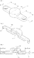
- FIG. 1 is a perspective view of a lens module according to a first embodiment
- FIG. 2 is a cross-sectional view of the lens module of FIG. 1 taken along lines A-A'
- FIG. 3 illustrates a plan view for a cross-sectional portion of the lens module of FIG. 2 .
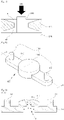
- the lens module 100 may include: a lens part 110; support parts 120 extending from the outside of the lens part 110; through holes H formed at each of the support parts 120.
- the lens part 110 has internally a light source receiving region 111 for receiving a printed circuit board (PCB) to which a light emitting diode is mounted, and includes a lens form having a curvature in a structure which protrudes to the outside so that light received in the light source receiving region 111 can be diffused to the outside.
- PCB printed circuit board
- the lens module 100 may be made using a transparent resin and the lens may include a fluorescent agent.
- the lens part 110 may be injected and molded with the resin containing the fluorescent agent, or may be produced in such a manner as to apply the fluorescent agent to transparent or translucent resin, glass or film.
- a light emitting diode receiving region 111b may be processed as a cavity having a convex curvature and a PCB receiving region intended for mounting light emitting diodes may be processed as a cavity corresponding to a shape of the PCB.
- the light source receiving region 111 having such a double structure When the light source receiving region 111 having such a double structure is formed, light penetrates elements having different refractive indexes while penetrating the lens part 110 and the light source receiving region in which an air layer resulting from the light emitting diode will be formed, so that a diffusing and scattering rate of the light can be increased. In addition to this, a diffusing and scattering rate can be further improved by a convex curvature of the light emitting diode receiving region 111b.
- the support part 120 may be implemented as a structure in a plate form which extends to be integrally formed with the outside of the lens part 110 and may be implemented in an integral structure with the lens part 110 using an injection molding method.
- the support part 120 may be combined with the lens part 110.
- the support part 120 may have a connection part X for connecting the lens part 110 to an outer structure such as a bezel part, a reflector or the like, and the connection part X may include a hole form or may include a protruding structure form in an embodiment which will be described later.
- connection part X is implemented in the structure of a through hole H that passes through the support part 110.
- the structure of through hole H may be configured to pass through the support part 110, or may be formed to be tapered from both surfaces of the support part 110 toward a central portion of the through hole.
- the through hole H be tapered from an upper surface of the support part 120 to portions a, c forming an inclination angle with a central portion b of a thickness of the support part 120.
- This structure is advantageous in that a bonding force can be improved by enabling a melt bonding surface to extend in a structure in which a melt bonding material is collected along a concave inclination of a tapered portion when an external connection element inserted into the through hole H later is bonded by a hot staking method.
- the second embodiment illustrates an example of the configuration of a light emitting diode package to which the lens module of the first embodiment is applied.
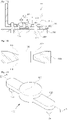
- FIGS. 4 and 5 illustrate the configuration of the light emitting diode package according to the second embodiment.
- the light emitting diode package may include the lens module described in the sections regarding FIGS. 1 to 3 , and a light source module 400 including a light emitting diode 410 accommodated inside a light source receiving region of the lens module 100, and a printed circuit board (PCB) 420 to which the light emitting diode 410 is mounted, and the light emitting diode package may further include a bezel part 200 having an opening into which the lens part 110 of the lens module 100 can be inserted.
- PCB printed circuit board
- the bezel part 200 may be formed as a reflector having a reflection property.
- the bezel part may be made of a material containing at least one of at least one of Ag, Al, Pt, Cr, Ni, a titanium oxide, a silicon oxide, an aluminum oxide, a magnesium fluoride, a tantalum oxide and a zinc oxide, or may be formed as a structure in which the aforesaid material is contained in a substrate, or a structure in which the aforesaid material is coated on a substrate.
- the bezel part 200 may include a side portion 210 and a lower surface portion 220 in which a bottom of the side portion 210 is bent, and an upper portion of the bezel part 200 is formed to be open. Moreover, one region of the lower surface portion 220 is open, and the lens part 110 of the lens module may be inserted into an opening position.
- the through hole H of the first embodiment may be formed in the support part 120 of the lens module 100, and the through hole H may be gradually tapered from an upper surface and a lower surface portion to a central portion.
- a bezel protrusion part 211 extending from a lower surface portion 220 of the bezel part may be connected to be inserted into the through hole H, and melt bonding of the bezel protrusion part and the through hole may be performed using a hot staking method and the like.
- melt bonding material is collected in tapered portions HI, H2 of the through hole H so that strong bonding between a surface of the support part of the lens module and a lower surface portion 220 of the bezel part can be realized.
- the light source receiving region 111 having a double structure in which the light emitting diode receiving region 111b is processed as a cavity having a convex curvature, and the PCB receiving region 111a for mounting the light emitting diode is process as a cavity corresponding to a shape of the PCB, is formed inside the lens module 100, so that light can penetrate constitutive materials having different refractive indexes, thereby increasing a diffusion and scattering rate of the light and further improving the diffusion and scattering rate thanks to the convex curvature of the light emitting diode receiving region 111b.
- FIGS. 6 and 7 illustrates the third embodiment according.
- the third embodiment is similar to the first embodiment, in that the light emitting diode package includes the lens module 100 of the first embodiment, and is configured such that the lens module 100 and the bezel part 200 are combined by providing a separate base plate 300.
- the base plate 300 is configured such that a plate protrusion part 320 in a protruding form is formed on a substrate 310.
- a plate protrusion part 320 in a protruding form is formed on a substrate 310.
- the third embodiment compared to the second embodiment, since the base plate 300 is added, the elements are increased.
- the third embodiment has a meaning, in that a light source module 400, the lens module 100 and the bezel part 200 can be stably supported from the bottom and can be bonded thanks to the base plate, and the third embodiment is also advantageous in that strong bonding can be realized by applying the lens module according to the first embodiment.
- a separate through hole having the same structure as that of the through hole H of the lens module 100 is formed in a position corresponding to the plate protrusion part 320, and a hot staking method is performed after the plate protrusion part 320 has been inserted into the separate through hole so that stronger bonding can be realized.
- the separate through hole may be tapered in the same manner as the structure of the through hole implemented in the lens module.
- FIG. 8 is a perspective concept view of a lens module according to a fourth embodiment.
- FIG. 9 is a cross-sectional view of the lens module of FIG. 7 taken along lines A-A'.
- the lens module 100 may include: the lens part 110; the support part 120 extending to the outside of the lens part 110; and the protrusion part 130 on the support part 120.
- the lens part 110 include the light source receiving region 111 for receiving the printed circuit board in which the light emitting diode is mounted, and has a lens-like shape having a curvature in a structure which protrudes to the outside, so that light accommodated in the light source receiving region 111 can be diffused to the outside.
- the lens module 100 may be made of a transparent resin, and the lens module 100 may contain a fluorescent agent.
- the lens part 110 may be injected and molded using resin containing the fluorescent agent, or may be produced by applying the fluorescent agent to transparent or translucence resin, glass or film.
- the light source receiving region 111 inside the lens part 110 may be implemented as a receiving space (cavity), and the light emitting diode receiving region 111b may be processed as a cavity having a convex curvature and the PCB receiving region 111a may be processed as a cavity corresponding to a shape of the PCB.
- the light source receiving region 111 having such a double structure When the light source receiving region 111 having such a double structure is formed, light can penetrate elements having different refractive indexes while penetrating the lens part and the light source receiving region 111 having an air layer from the light emitting diode, thereby enabling the improvement of a diffusing and scattering rate of the light and the diffusing and scattering rate to be further improved thanks to the convex curvature of the light emitting diode receiving region 111b.
- the support part 120 may be implemented as a structure in a flat form which extends to be integrally formed with the outside of the lens part 110, and may be implemented in an integral structure with the lens part 110 using an injection molding method.
- the support part may be configured to be combined with the lens part 110.
- the present embodiment may include the protrusion part 131 which is configured to protrude on the support part 120.
- the protrusion part 131 may be formed on one surface which is an upper surface of the support part 120, and the lens part 110 may be formed as a cylindrical structure without being limited thereto.
- the lens part may have various prismatic shapes, and a width, a length and number of the protrusion structure and a shape of a cross section of the protrusion structure may be variously changed.
- the protrusion part 131 may be coupled to a connection hole or a connection part using an insertion or melt bonding method and the like
- the lens module according to the fifth embodiment is advantageous in that a production process can be simplified because a connection member is provided at the lens module so that a combination with an object to be combined can be easily performed without a separate outer element.
- FIGS. 10 and 11 illustrate the embodiment of a light emitting diode package to which the structure of the lens module according to a fifth embodiment of is applied.
- the lens module 100 according to the fourth embodiment in FIG. 8 may have the protrusion part 131 on a surface of the support part 120, and in the present embodiment, a structure in which the protrusion part 131 is only provided on an upper surface of the support part 120 is described and in the sections regarding embodiments which will be described later, modified structures will be described.
- the light emitting diode package to which the lens module according to the fifth embodiment is applied may include the lens module 100 and the light source module 400 including the light emitting diode 410 accommodated inside a light source receiving region of the lens module 100, and the printed circuit board 420 to which the light emitting diode 410 is mounted, and the light emitting diode package may further include the bezel part 200 having an opening into which the lens part 110 of the lens module 100 can be inserted.
- the bezel part may be formed as a reflector having a reflection property.
- the bezel part may be made of a material containing at least one of at least one of Ag, Al, Pt, Cr, Ni, a titanium oxide, a silicon oxide, an aluminum oxide, a magnesium fluoride, a tantalum oxide and a zinc oxide, or may be formed as a structure in which the aforesaid material is contained in a substrate, or a structure in which the aforesaid material is coated on a substrate.
- the bezel part 200 may include a side portion 210 and a lower surface portion 220 formed to be bent from a bottom of the side portion 210, and an upper portion of the bezel part has an open structure.
- one area of the lower surface portion 220 is open, and accordingly, the lens part 110 of the lens module 100 is inserted into the lower surface portion 220 via the open area.
- a bezel through-hole 221 may be formed in the lower surface portion 220 of the bezel part 200 so that the protrusion part 131 of the lens module can be inserted, and the lens module 100 and the bezel part 200 may be bonded by a hot staking method after and the protrusion part 131 of the lens module 100 has been inserted into and connected to the bezel through hole 221,
- the bonding portion may be implemented in a structure in which a pattern in a concave groove form is formed, rather than the structure in which the bezel through hole passes through the lower surface portion.
- the bonding portion 221 in a hole structure provided at the lower surface portion 220 of the bezel part 200 may be configured to have the portions HI, H2 that are gradually tapered from one surface or both surfaces of the lower surface portion 220 of the bezel part 200 to a central portion thereof.
- the lens module 100 of the fifth embodiment When the lens module 100 of the fifth embodiment is applied, there is a need to dispose a separate support plate in a lower portion of the lens module upon bonding the lens module 100 and the bezel part 200. Thus, a strong bonding force with the bezel part 200 can be simply realized by the lens module 100 so that the light emitting diode package having reliability can be realized at a lower cost.
- the lens module illustrated in FIG. 12 has a modified structure of that of the fourth embodiment and is different from that of the fourth embodiment, in that the protrusion parts 131, 132 are formed on one surface of the support part 120 and another surface opposite to the one surface, respectively.
- the first protrusion part 131 is formed on the upper surface of the support part 120
- the second protrusion part 132 is formed on the lower surface of the support part 120.
- the first protrusion 131 may be combined with the bezel part 200 as described in the sections regarding FIG. 10 , and the second protrusion 132 is J bonded to the base plate 300 which is an external structure.
- FIG. 13 shows the light emitting diode package to which the lens module 100 presented in FIG. 12 is applied and the light emitting diode package has a difference, in that the second protrusion part 132 is added to the lower surface of the support part 120 of the lens module 100.
- the first protrusion part 131 of the lens module 100 is bonded to the lower surface of the bezel part 200 as shown in the embodiment of FIG. 10 , and the plate through-hole 320 of the base plate 300 is formed so that the second protrusion part 132 of the lens module 100 can be combined with the plate through hole 320 in such a manner as to pass through the plate through hole 320.
- melt boding is performed using a hot staking method, the base plate 300 and the bezel part 200 located at the upper portion are bonded via the lens module so that stronger bonding can be realized.
- the plate through-hole 320 provided at the base plate 300 is implemented to be gradually tapered toward the central portion thereof.
- a melt bonding material is collected in tapered portions H3, H4 of the plate through-hole 320 so that the surface of the lens module 100 and the lower surface portion 220 of the bezel part 200 can be strongly bonded.
- the plate through hole 320 is formed to be tapered toward a central portion of the base plate 300.
- the plate through-hole 320 may be formed in a concave pattern structure.
- the sixth embodiment compared to the fifth embodiment, even though the base plate 300 is added, it is advantageous in that the light source module 400, the lens module 100 and the bezel part 200 can be stably supported and bonded, and that stronger bonding can be realized by applying the lens module according to the fourth embodiment.
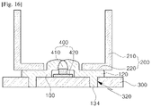
- the seventh embodiment illustrated in FIGS. 15 and 16 is identical to the other embodiments, in that the lens 110 and the support part 120 are provided, but is different from the other embodiments, in that a second protrusion part 134, which is a protruding structure, is only formed on a lower surface portion of the support part 120.
- the seventh embodiment has a structure in which the lens module 100 and the bezel part 200 are bonded using an adhesive material, and this structure may be applied to a case for which a more strong bonding force between the lens module 100 and the base plate 300 of a lower portion is needed.
- the light emitting diode package to which the seventh embodiment is applied is configured such that the second protrusion part 134 is inserted into and welded in the plate through hole 320 of the base plate 300, and the plate through hole 320 is formed to be gradually tapered toward a central portion thereof.
Description
- Embodiments of the present invention relate to a light emitting diode package and a lens module included in the light emitting device package.
- A light emitting diode (LED) is a semiconductor device that converts electrical energy into light energy. The LED may produce light having various wavelengths (colors) by controlling the components of a compound semiconductor, and the output from the LED may range from red, green, blue-violet and the like. The LED may emit white light having excellent efficiency by combining colors using a fluorescent material.
- LEDs, compared with conventional light sources such as a fluorescent lamp, an incandescent lamp and so on, have advantages including lower energy consumption, semi-permanent life span, improved response speed, stability, environmental friendliness and the like. Accordingly, the scope of application for LEDs has been extending to a light-emitting diode backlight to replace a cold cathode fluorescent lamp (CCFL) constituting a backlight of an LCD (Liquid Crystal Display) device, a white light-emitting diode lighting device to replace a fluorescent lamp or an incandescent lamp, a car headlight, a signal lamp and the like.
- According to a conventional art, a light emitting device chip is combined with a predetermined package body and resin containing a fluorescent substance is provided on the light-emitting device chip, and a lens is formed on the resin, thereby constituting a light emitting device package.
- In particular, since the lens combined with the light emitting device package has a low bonding property with a structure such as an external reflector, a bezel and the like, bonding reliability is ensured by a fixing method using a fixing member with a structure such as a bottom plate and the like for combining the lens with the separate light emitting device package, as a base of lower support. However, it is problematic in that an inconvenient process and an increase in production costs are caused.
US2008/151547 ,US2012/243239 ,WO2008/003167 andUS2011/273876 are examples of light emitting diode package. - Embodiments of the inventions are intended to solve the above problems, and an aspect of the present invention provides a lens module that enables the simplification of a structure and a production process by forming connection parts combined with external bezel parts in a lens itself with regard to a lens structure for a light emitting device to easily combine the bezel parts and a lens part even without the element of a separate base plate.
- According to the present invention, there is provided a light emitting diode package including the features of claim 1. A lens module, includes: a lens part; support parts extending from the outside of the lens part; and connection parts formed on the support parts, respectively.
- According to an aspect of the present disclosure there is provided a light emitting diode package, including: a lens module including a lens part, support parts extending from the outside of the lens part and connection parts formed on the support parts, respectively; a light source module accommodated inside the lens part of the lens module; and bezel parts each having an opening formed at a region corresponding to the lens part of the lens module.
- According to some embodiments with regard to a lens structure for a light emitting diode, as connection parts combined with external bezel parts are formed in a lens itself, the bezel parts and a lens part are easily combined even without the element of a separate base plate so that the structure and a production process can be simplified, and thus a reduction in production costs can be realized.
- Also, it is advantageous in that, even though the base plate is provided, the connection parts combined with the base plate are formed in the lens itself so that the light emitting diode package in a structure having more high reliability can be implemented.
-
-
FIG. 1 is a perspective view of a lens module according to a first embodiment as disclosed; -
FIG. 2 is a cross-sectional view of the lens module offig. 1 taken along lines A-A'; -
FIG. 3 is a cross-sectional view of the lens module offig. 1 ; -
FIGS. 4 and 5 are cross-sectional views of a light emitting diode package according to a second embodiment as disclosed; -
FIGS. 6 and7 are cross-sectional views of a light emitting diode package according to a third embodiment as disclosed; -
FIG. 8 is a perspective view of a lens module according to a fourth embodiment as disclosed; -
FIG. 9 is a cross-sectional view of the lens module offig. 8 taken along lines A-A'; -
FIGS. 10 and 11 are cross-sectional views of a light emitting diode package according to a fifth embodiment as disclosed; -
FIG. 12 is a perspective view of a lens module according to a sixth embodiment as disclosed; -
FIGS. 13 and 14 are cross-sectional views of a light emitting diode package offig. 12 ; -
FIG. 15 is a perspective view of a lens module according to a seventh embodiment as disclosed; and -
FIG. 16 is a cross-sectional view of a light emitting diode package according to another embodiment as disclosed. - Hereinafter, the configurations and operations according to embodiments disclosed will be described in detail with reference to the accompanying drawings. Regardless of reference numerals of the drawings, the elements having the similar functions and operations of the drawings are given the same reference numerals. Terms such as a first term and a second term may be used for explaining various constitutive elements, but the constitutive elements should not be limited to these terms. These terms is used only for the purpose for distinguishing a constitutive element from other constitutive element.
- The embodiments will be clearly shown based on the accompany drawings and the description of the embodiments. With regard to the description of the embodiments, it will also be understood that when an element is referred to as being "on" another element, substrate, layer, region, pad or pattern, it can be directly on the other element, substrate, layer, region, pad or pattern, or intervening elements may also be present. Further, it will be understood that when an element is referred to as being "under" another element, it can be directly under, or one or more intervening elements may also be present. In the drawings, the thicknesses of layers and regions may be exaggerated for clarity. Hereinafter, the embodiments will be described with reference to the accompanying drawings. The embodiments shown in
figures 1 to 11 are not covered by the claimed invention. -
FIG. 1 is a perspective view of a lens module according to a first embodiment,FIG. 2 is a cross-sectional view of the lens module ofFIG. 1 taken along lines A-A', andFIG. 3 illustrates a plan view for a cross-sectional portion of the lens module ofFIG. 2 . - Referring to
FIGS. 1 to 3 , thelens module 100 according to the first embodiment may include: alens part 110;support parts 120 extending from the outside of thelens part 110; through holes H formed at each of thesupport parts 120. - As illustrated in
FIG. 2 , thelens part 110 has internally a lightsource receiving region 111 for receiving a printed circuit board (PCB) to which a light emitting diode is mounted, and includes a lens form having a curvature in a structure which protrudes to the outside so that light received in the lightsource receiving region 111 can be diffused to the outside. - Also, the
lens module 100 may be made using a transparent resin and the lens may include a fluorescent agent. Thelens part 110 may be injected and molded with the resin containing the fluorescent agent, or may be produced in such a manner as to apply the fluorescent agent to transparent or translucent resin, glass or film. - Furthermore, even though the light
source receiving region 111 inside thelens part 110 may be implemented as a general internal receiving space (cavity), a light emittingdiode receiving region 111b may be processed as a cavity having a convex curvature and a PCB receiving region intended for mounting light emitting diodes may be processed as a cavity corresponding to a shape of the PCB. - When the light
source receiving region 111 having such a double structure is formed, light penetrates elements having different refractive indexes while penetrating thelens part 110 and the light source receiving region in which an air layer resulting from the light emitting diode will be formed, so that a diffusing and scattering rate of the light can be increased. In addition to this, a diffusing and scattering rate can be further improved by a convex curvature of the light emittingdiode receiving region 111b. - The
support part 120 may be implemented as a structure in a plate form which extends to be integrally formed with the outside of thelens part 110 and may be implemented in an integral structure with thelens part 110 using an injection molding method. - Of course, after the
support part 120 has been produced as a structure separated from thelens part 110, the support part may be combined with thelens part 110. - In particular, as illustrated in
FIG. 3 , in the present embodiment, thesupport part 120 may have a connection part X for connecting thelens part 110 to an outer structure such as a bezel part, a reflector or the like, and the connection part X may include a hole form or may include a protruding structure form in an embodiment which will be described later. - The embodiments of the lens module of
FIGS. 1 to 3 show that the connection part X is implemented in the structure of a through hole H that passes through thesupport part 110. - In particular, as illustrated in
FIG. 2 , the structure of through hole H may be configured to pass through thesupport part 110, or may be formed to be tapered from both surfaces of thesupport part 110 toward a central portion of the through hole. - That is, as illustrated in
FIG. 3 , it is more preferable that the through hole H be tapered from an upper surface of thesupport part 120 to portions a, c forming an inclination angle with a central portion b of a thickness of thesupport part 120. This structure is advantageous in that a bonding force can be improved by enabling a melt bonding surface to extend in a structure in which a melt bonding material is collected along a concave inclination of a tapered portion when an external connection element inserted into the through hole H later is bonded by a hot staking method. - The second embodiment illustrates an example of the configuration of a light emitting diode package to which the lens module of the first embodiment is applied.
-
FIGS. 4 and 5 illustrate the configuration of the light emitting diode package according to the second embodiment. - Referring to
FIGS. 4 and 5 , the light emitting diode package according to the present embodiment may include the lens module described in the sections regardingFIGS. 1 to 3 , and alight source module 400 including alight emitting diode 410 accommodated inside a light source receiving region of thelens module 100, and a printed circuit board (PCB) 420 to which thelight emitting diode 410 is mounted, and the light emitting diode package may further include abezel part 200 having an opening into which thelens part 110 of thelens module 100 can be inserted. - The
bezel part 200 may be formed as a reflector having a reflection property. In this case, the bezel part may be made of a material containing at least one of at least one of Ag, Al, Pt, Cr, Ni, a titanium oxide, a silicon oxide, an aluminum oxide, a magnesium fluoride, a tantalum oxide and a zinc oxide, or may be formed as a structure in which the aforesaid material is contained in a substrate, or a structure in which the aforesaid material is coated on a substrate. - The
bezel part 200 may include aside portion 210 and alower surface portion 220 in which a bottom of theside portion 210 is bent, and an upper portion of thebezel part 200 is formed to be open. Moreover, one region of thelower surface portion 220 is open, and thelens part 110 of the lens module may be inserted into an opening position. - In particular, the through hole H of the first embodiment may be formed in the
support part 120 of thelens module 100, and the through hole H may be gradually tapered from an upper surface and a lower surface portion to a central portion. - A
bezel protrusion part 211 extending from alower surface portion 220 of the bezel part may be connected to be inserted into the through hole H, and melt bonding of the bezel protrusion part and the through hole may be performed using a hot staking method and the like. - At this time, a melt bonding material is collected in tapered portions HI, H2 of the through hole H so that strong bonding between a surface of the support part of the lens module and a
lower surface portion 220 of the bezel part can be realized. - Accordingly, in the embodiment of
FIG. 4 , there is no need to combine thelens module 100 and thebezel part 200 because the separate support plate is disposed in a lower portion of thelens module 100. Thus, a strong bonding force with thebezel part 200 may be simply implemented by thelens module 100, so that the light emitting diode package having reliability can be implemented at a lower cost. - Also, the light
source receiving region 111 having a double structure, in which the light emittingdiode receiving region 111b is processed as a cavity having a convex curvature, and thePCB receiving region 111a for mounting the light emitting diode is process as a cavity corresponding to a shape of the PCB, is formed inside thelens module 100, so that light can penetrate constitutive materials having different refractive indexes, thereby increasing a diffusion and scattering rate of the light and further improving the diffusion and scattering rate thanks to the convex curvature of the light emittingdiode receiving region 111b. -
FIGS. 6 and7 illustrates the third embodiment according. - Referring to
FIGS. 6 and7 , the third embodiment is similar to the first embodiment, in that the light emitting diode package includes thelens module 100 of the first embodiment, and is configured such that thelens module 100 and thebezel part 200 are combined by providing aseparate base plate 300. - The
base plate 300 is configured such that aplate protrusion part 320 in a protruding form is formed on asubstrate 310. Thus, when theplate protrusion part 320 is adhered bonded to thelower surface portion 220 of thebezel part 200 by passing through the through hole H of thelens module 100 and melt-bonding is performed by a hot staking (HS) method, theplate protrusion part 320 is melt-bonded and a melting bonding material is collected in tapered portions HI, H2 of the through hole H so that a surface of thelens module 100 can be strongly bonded to thelower surface portion 220 of the bezel part. - In the third embodiment, compared to the second embodiment, since the
base plate 300 is added, the elements are increased. In spite of this face, the third embodiment has a meaning, in that alight source module 400, thelens module 100 and thebezel part 200 can be stably supported from the bottom and can be bonded thanks to the base plate, and the third embodiment is also advantageous in that strong bonding can be realized by applying the lens module according to the first embodiment. - In particular, even though it is not illustrated, in the
lower surface portion 220 of thebezel part 200, a separate through hole having the same structure as that of the through hole H of thelens module 100 is formed in a position corresponding to theplate protrusion part 320, and a hot staking method is performed after theplate protrusion part 320 has been inserted into the separate through hole so that stronger bonding can be realized. - Of course, in this case, the separate through hole may be tapered in the same manner as the structure of the through hole implemented in the lens module.
-
FIG. 8 is a perspective concept view of a lens module according to a fourth embodiment.FIG. 9 is a cross-sectional view of the lens module ofFIG. 7 taken along lines A-A'. - Referring to
FIGS. 8 and 9 , thelens module 100 according to the fourth embodiment may include: thelens part 110; thesupport part 120 extending to the outside of thelens part 110; and theprotrusion part 130 on thesupport part 120. - The
lens part 110 include the lightsource receiving region 111 for receiving the printed circuit board in which the light emitting diode is mounted, and has a lens-like shape having a curvature in a structure which protrudes to the outside, so that light accommodated in the lightsource receiving region 111 can be diffused to the outside. - Also, the
lens module 100 may be made of a transparent resin, and thelens module 100 may contain a fluorescent agent. Thelens part 110 may be injected and molded using resin containing the fluorescent agent, or may be produced by applying the fluorescent agent to transparent or translucence resin, glass or film. - Furthermore, as illustrated in
FIG. 9 , the lightsource receiving region 111 inside thelens part 110 may be implemented as a receiving space (cavity), and the light emittingdiode receiving region 111b may be processed as a cavity having a convex curvature and thePCB receiving region 111a may be processed as a cavity corresponding to a shape of the PCB. - When the light
source receiving region 111 having such a double structure is formed, light can penetrate elements having different refractive indexes while penetrating the lens part and the lightsource receiving region 111 having an air layer from the light emitting diode, thereby enabling the improvement of a diffusing and scattering rate of the light and the diffusing and scattering rate to be further improved thanks to the convex curvature of the light emittingdiode receiving region 111b. - The
support part 120 may be implemented as a structure in a flat form which extends to be integrally formed with the outside of thelens part 110, and may be implemented in an integral structure with thelens part 110 using an injection molding method. Of course, as the support part is produced as a separate structure from thelens part 110, the support may be configured to be combined with thelens part 110. - In particular, the present embodiment may include the
protrusion part 131 which is configured to protrude on thesupport part 120. - As illustrate in
FIGS. 8 and 9 , theprotrusion part 131 may be formed on one surface which is an upper surface of thesupport part 120, and thelens part 110 may be formed as a cylindrical structure without being limited thereto. Thus, the lens part may have various prismatic shapes, and a width, a length and number of the protrusion structure and a shape of a cross section of the protrusion structure may be variously changed. - Also, the
protrusion part 131 may be coupled to a connection hole or a connection part using an insertion or melt bonding method and the like - The lens module according to the fifth embodiment is advantageous in that a production process can be simplified because a connection member is provided at the lens module so that a combination with an object to be combined can be easily performed without a separate outer element.
-
FIGS. 10 and 11 illustrate the embodiment of a light emitting diode package to which the structure of the lens module according to a fifth embodiment of is applied. - As illustrated in
FIG. 10 , thelens module 100 according to the fourth embodiment inFIG. 8 may have theprotrusion part 131 on a surface of thesupport part 120, and in the present embodiment, a structure in which theprotrusion part 131 is only provided on an upper surface of thesupport part 120 is described and in the sections regarding embodiments which will be described later, modified structures will be described. - As illustrated in
FIG. 10 , the light emitting diode package to which the lens module according to the fifth embodiment is applied may include thelens module 100 and thelight source module 400 including thelight emitting diode 410 accommodated inside a light source receiving region of thelens module 100, and the printedcircuit board 420 to which thelight emitting diode 410 is mounted, and the light emitting diode package may further include thebezel part 200 having an opening into which thelens part 110 of thelens module 100 can be inserted. - The bezel part may be formed as a reflector having a reflection property. In this case, In this case, the bezel part may be made of a material containing at least one of at least one of Ag, Al, Pt, Cr, Ni, a titanium oxide, a silicon oxide, an aluminum oxide, a magnesium fluoride, a tantalum oxide and a zinc oxide, or may be formed as a structure in which the aforesaid material is contained in a substrate, or a structure in which the aforesaid material is coated on a substrate.
- The
bezel part 200 may include aside portion 210 and alower surface portion 220 formed to be bent from a bottom of theside portion 210, and an upper portion of the bezel part has an open structure. - Moreover, one area of the
lower surface portion 220 is open, and accordingly, thelens part 110 of thelens module 100 is inserted into thelower surface portion 220 via the open area. - Also, a bezel through-
hole 221 may be formed in thelower surface portion 220 of thebezel part 200 so that theprotrusion part 131 of the lens module can be inserted, and thelens module 100 and thebezel part 200 may be bonded by a hot staking method after and theprotrusion part 131 of thelens module 100 has been inserted into and connected to the bezel throughhole 221, - In the illustrated embodiment, even though the bezel through
hole 221 is implemented to pass through thelower surface portion 220 of thebezel part 200, according to circumstances, the bonding portion may be implemented in a structure in which a pattern in a concave groove form is formed, rather than the structure in which the bezel through hole passes through the lower surface portion. - In this case, as illustrated in
FIG. 11 , thebonding portion 221 in a hole structure provided at thelower surface portion 220 of thebezel part 200 may be configured to have the portions HI, H2 that are gradually tapered from one surface or both surfaces of thelower surface portion 220 of thebezel part 200 to a central portion thereof. - This is also intended to realize a strong bonding force as a melt boding solution is collected in the regions having a tapered structure upon hot staking of the
protrusion 131. - When the
lens module 100 of the fifth embodiment is applied, there is a need to dispose a separate support plate in a lower portion of the lens module upon bonding thelens module 100 and thebezel part 200. Thus, a strong bonding force with thebezel part 200 can be simply realized by thelens module 100 so that the light emitting diode package having reliability can be realized at a lower cost. - The lens module illustrated in
FIG. 12 has a modified structure of that of the fourth embodiment and is different from that of the fourth embodiment, in that theprotrusion parts support part 120 and another surface opposite to the one surface, respectively. - That is, the
first protrusion part 131 is formed on the upper surface of thesupport part 120, and thesecond protrusion part 132 is formed on the lower surface of thesupport part 120. - Accordingly, the
first protrusion 131 may be combined with thebezel part 200 as described in the sections regardingFIG. 10 , and thesecond protrusion 132 is J bonded to thebase plate 300 which is an external structure. -
FIG. 13 shows the light emitting diode package to which thelens module 100 presented inFIG. 12 is applied and the light emitting diode package has a difference, in that thesecond protrusion part 132 is added to the lower surface of thesupport part 120 of thelens module 100. - In particular, as illustrated in
FIGS. 12 and13 , thefirst protrusion part 131 of thelens module 100 is bonded to the lower surface of thebezel part 200 as shown in the embodiment ofFIG. 10 , and the plate through-hole 320 of thebase plate 300 is formed so that thesecond protrusion part 132 of thelens module 100 can be combined with the plate throughhole 320 in such a manner as to pass through the plate throughhole 320. When melt boding is performed using a hot staking method, thebase plate 300 and thebezel part 200 located at the upper portion are bonded via the lens module so that stronger bonding can be realized. - At this time, as illustrated in
FIG. 14 , the plate through-hole 320 provided at thebase plate 300 is implemented to be gradually tapered toward the central portion thereof. A melt bonding material is collected in tapered portions H3, H4 of the plate through-hole 320 so that the surface of thelens module 100 and thelower surface portion 220 of thebezel part 200 can be strongly bonded. - That is, the plate through
hole 320 is formed to be tapered toward a central portion of thebase plate 300. In another not claimed embodiment, the plate through-hole 320 may be formed in a concave pattern structure. - In the sixth embodiment, compared to the fifth embodiment, even though the
base plate 300 is added, it is advantageous in that thelight source module 400, thelens module 100 and thebezel part 200 can be stably supported and bonded, and that stronger bonding can be realized by applying the lens module according to the fourth embodiment. - The seventh embodiment illustrated in
FIGS. 15 and16 is identical to the other embodiments, in that thelens 110 and thesupport part 120 are provided, but is different from the other embodiments, in that asecond protrusion part 134, which is a protruding structure, is only formed on a lower surface portion of thesupport part 120. - At this time, the seventh embodiment has a structure in which the
lens module 100 and thebezel part 200 are bonded using an adhesive material, and this structure may be applied to a case for which a more strong bonding force between thelens module 100 and thebase plate 300 of a lower portion is needed. - As illustrated in
FIG. 16 , the light emitting diode package to which the seventh embodiment is applied is configured such that thesecond protrusion part 134 is inserted into and welded in the plate throughhole 320 of thebase plate 300, and the plate throughhole 320 is formed to be gradually tapered toward a central portion thereof. - As previously described, in the detailed description of the invention, having described the detailed exemplary embodiments, it should be apparent that modifications and variations can be made by persons skilled without deviating from the scope of the invention. Therefore, it is to be understood that the foregoing is illustrative of the present invention and is not to be construed as limited to the specific embodiments disclosed. The invention is defined by the appended claims.
Claims (11)
- A light emitting diode package, comprising:a base plate (300);a lens module (100) disposed on the base plate (300); anda bezel part (200) having an opening,wherein the lens module (100) comprises:a lens part (110) including a light source receiving region (111);a first support part (120) extending in a first lateral direction away from an outside of the lens part (110);a first protrusion part (134) extending from a lower surface of the first support part (120) into a first through hole of the base plate (300);a second support part (120) extending in a second lateral direction opposite to said first lateral direction away from the outside of the lens part (110); anda second protrusion part (134) extending from the lower surface of the second support part (120) into a second through hole of the base plate (300),wherein the first protrusion part(134) and the second protrusion part (134) are welded to the base plate (300), the first support part (120) includes an inner end, an outer end and a first region disposed between the inner end and the outer end, the inner end of the first support part (120) is disposed adjacent to the lens part (110), the outer end of the first support part (120) farthest away from the lens part (110) in the first lateral direction and having a first edge, the first region of the first support part (120) has a constant thickness and constant width, the entire lower surface of the lens module (100) except the light source receiving region (111) is in direct physical contact with the base plate (300), a thickness of the lens part (110) is minimum at a central portion in correspondence of which a light emitting diode is disposed, the first and the second through hole (320) of the base plate (300) are formed to be gradually tapered toward a central portion thereof, the bezel part (200) includes a side portion (210) and a lower surface portion (220) in which a bottom of the side portion (210) is bent, an upper portion of the bezel part (200) is opened, one region of the lower surface portion (220) is open, and the lens part (110) of the lens module (100) is inserted into the opening of the bezel part (200), and whereinthe second support part (120) includes an inner end, an outer end and first region disposed between the inner end and the outer end, the inner end of the second support part (120) is disposed adjacent to the lens part(110), the outer end of the second support part (120) farthest away from the lens part in the second lateral direction and having a second edge, the first region of the second support part (120) has a constant thickness and constant width.
- The light emitting diode package of claim 1, wherein the first protrusion part (134) is positioned on the lower surface of the first support part (120) such that it is spaced apart from the first edge, and
wherein the second protrusion part (134) is positioned on the lower surface of the second support part (120) such that it is spaced apart from the second edge. - The light emitting diode package of claim 1, wherein the lower surfaces of the inner end and the outer end of the first support part (120) are in direct physical contact with the base plate (300).
- The light emitting diode package of claim 3, wherein the lower surfaces of the inner end and the outer end of the second support part (120) are in direct physical contact with the base plate (300).
- The light emitting diode package of claim 1, wherein a portion of the lower surface of the lens part (110) is parallel to the lower surface of the second support part (120).
- The light emitting diode package of claim 1, wherein the lens part (110) is disposed between the first lateral direction and the second lateral direction.
- The light emitting diode package of claim 1, wherein the first protrusion part (134) is welded to the base plate in the first through hole.
- The light emitting diode package of claim 1, wherein the first protrusion part (134) is welded to the base plate (300) in the first through hole, and wherein the second protrusion part (134) is welded to the base plate in the second through hole (300).
- The light emitting diode package of claim 1, wherein the first protrusion part (134) extends completely through the first through hole.
- The light emitting diode package of claim 1, wherein the first protrusion part (134) extends completely through the first though hole, and wherein the second protrusion part (134) extends completely through the second though hole.
- The light emitting diode package of claim 1, wherein the first protrusion part (134) is in direct physical contact with an inner surface of the first through hole.
Applications Claiming Priority (3)
| Application Number | Priority Date | Filing Date | Title |
|---|---|---|---|
| KR1020130119298A KR102024297B1 (en) | 2013-10-07 | 2013-10-07 | Lens module and light emitting device package including the same |
| KR1020130148574A KR102137744B1 (en) | 2013-12-02 | 2013-12-02 | Lens module and light emitting device package including the same |
| PCT/KR2014/009412 WO2015053527A1 (en) | 2013-10-07 | 2014-10-07 | Lens module and light emitting device package comprising same |
Publications (3)
| Publication Number | Publication Date |
|---|---|
| EP3056806A1 EP3056806A1 (en) | 2016-08-17 |
| EP3056806A4 EP3056806A4 (en) | 2016-11-16 |
| EP3056806B1 true EP3056806B1 (en) | 2022-09-28 |
Family
ID=52813305
Family Applications (1)
| Application Number | Title | Priority Date | Filing Date |
|---|---|---|---|
| EP14852517.3A Active EP3056806B1 (en) | 2013-10-07 | 2014-10-07 | Lens module and light emitting device package comprising same |
Country Status (5)
| Country | Link |
|---|---|
| US (1) | US10107474B2 (en) |
| EP (1) | EP3056806B1 (en) |
| JP (1) | JP6764785B2 (en) |
| CN (1) | CN105814362B (en) |
| WO (1) | WO2015053527A1 (en) |
Families Citing this family (2)
| Publication number | Priority date | Publication date | Assignee | Title |
|---|---|---|---|---|
| FR3068482B1 (en) * | 2017-06-29 | 2019-08-09 | Valeo Vision Belgique | OPTICAL MODULE FOR LIGHTING DEVICE |
| US11372258B2 (en) * | 2020-02-13 | 2022-06-28 | Pixart Imaging Inc. | Lens piece, lens assembly and imaging device including the same |
Family Cites Families (16)
| Publication number | Priority date | Publication date | Assignee | Title |
|---|---|---|---|---|
| JPH08234071A (en) * | 1995-02-27 | 1996-09-13 | Kyocera Corp | Image device |
| DE102004051379A1 (en) * | 2004-08-23 | 2006-03-23 | Osram Opto Semiconductors Gmbh | Device for an optoelectronic component and component with an optoelectronic component and a device |
| DE102005033709B4 (en) | 2005-03-16 | 2021-12-16 | OSRAM Opto Semiconductors Gesellschaft mit beschränkter Haftung | Light emitting module |
| JP5513704B2 (en) * | 2005-08-22 | 2014-06-04 | 株式会社朝日ラバー | Lens body |
| US7906794B2 (en) * | 2006-07-05 | 2011-03-15 | Koninklijke Philips Electronics N.V. | Light emitting device package with frame and optically transmissive element |
| JP2009071186A (en) | 2007-09-14 | 2009-04-02 | Stanley Electric Co Ltd | Led unit |
| JP4836984B2 (en) * | 2008-03-21 | 2011-12-14 | コイズミ照明株式会社 | Lens, lens mounting substrate, and lighting device |
| US20110057557A1 (en) * | 2009-09-08 | 2011-03-10 | Hong Kong Applied Science And Technology Research Institute Co. Ltd. | Projection led module and method of making a projection led module |
| CN102959324A (en) * | 2010-05-04 | 2013-03-06 | 照明器控股有限公司 | Thermoplastic stake mounting system and method |
| KR101131152B1 (en) | 2010-07-02 | 2012-04-02 | 노현종 | Led diffusion lense, light diffusing sheet using it and light apparatus having it |
| JP5610935B2 (en) * | 2010-09-03 | 2014-10-22 | 矢崎総業株式会社 | Condenser lens |
| EP2682797B1 (en) * | 2011-03-01 | 2015-11-25 | FUJIFILM Corporation | Method for manufacturing lens module, and lens module |
| JP5573746B2 (en) * | 2011-03-23 | 2014-08-20 | 豊田合成株式会社 | Lamp unit |
| JP5687131B2 (en) * | 2011-05-11 | 2015-03-18 | 矢崎総業株式会社 | LED lighting unit |
| JP2012252890A (en) * | 2011-06-03 | 2012-12-20 | Yazaki Corp | Waterproof led lighting unit |
| JP2013134956A (en) * | 2011-12-27 | 2013-07-08 | Toshiba Lighting & Technology Corp | Lighting fixture |
-
2014
- 2014-10-07 JP JP2016520598A patent/JP6764785B2/en active Active
- 2014-10-07 EP EP14852517.3A patent/EP3056806B1/en active Active
- 2014-10-07 US US15/027,839 patent/US10107474B2/en active Active
- 2014-10-07 CN CN201480066993.0A patent/CN105814362B/en active Active
- 2014-10-07 WO PCT/KR2014/009412 patent/WO2015053527A1/en active Application Filing
Also Published As
| Publication number | Publication date |
|---|---|
| EP3056806A1 (en) | 2016-08-17 |
| US10107474B2 (en) | 2018-10-23 |
| JP6764785B2 (en) | 2020-10-07 |
| JP2016534545A (en) | 2016-11-04 |
| EP3056806A4 (en) | 2016-11-16 |
| US20160265739A1 (en) | 2016-09-15 |
| WO2015053527A1 (en) | 2015-04-16 |
| CN105814362A (en) | 2016-07-27 |
| CN105814362B (en) | 2020-03-10 |
Similar Documents
| Publication | Publication Date | Title |
|---|---|---|
| US9362461B2 (en) | Light emitting device and lighting system having the same | |
| KR101055023B1 (en) | Backlight unit and display device using same | |
| US9184349B2 (en) | Light emitting device, adhesive having surface roughness, and lighting system having the same | |
| KR20120132926A (en) | Light emitting device module and lighting system including the same | |
| KR101055081B1 (en) | Light emitting device, light emitting device manufacturing method and backlight unit | |
| EP3056806B1 (en) | Lens module and light emitting device package comprising same | |
| KR20150109591A (en) | Light emitting device package | |
| TWI573245B (en) | Light emitting diode light bar | |
| US9748452B2 (en) | Light-emitting element package | |
| JP6021485B2 (en) | Semiconductor light emitting device with optical member | |
| KR102024297B1 (en) | Lens module and light emitting device package including the same | |
| KR102137744B1 (en) | Lens module and light emitting device package including the same | |
| KR102029795B1 (en) | Light emitting device and lighting systme having thereof | |
| KR102110477B1 (en) | Light emitting device and lighting system having the same | |
| KR102019503B1 (en) | Light emitting device and lighting system | |
| KR102101367B1 (en) | Light emitting device | |
| KR20170052208A (en) | Optical plate, lighting device, and lighting module | |
| KR102131348B1 (en) | Light emitting device package | |
| KR101722627B1 (en) | Light Emitting Device Module | |
| KR102402259B1 (en) | A light emitting device package | |
| KR102142717B1 (en) | Light emitting device and lighting systme having thereof | |
| KR101831278B1 (en) | Light-emitting device | |
| KR102019504B1 (en) | Light emitting device and lighting system | |
| KR20240001598A (en) | Lighting module and lighting apparatus having thereof | |
| KR20140057930A (en) | Light emitting device and lighting systme having thereof |
Legal Events
| Date | Code | Title | Description |
|---|---|---|---|
| PUAI | Public reference made under article 153(3) epc to a published international application that has entered the european phase |
Free format text: ORIGINAL CODE: 0009012 |
|
| 17P | Request for examination filed |
Effective date: 20160506 |
|
| AK | Designated contracting states |
Kind code of ref document: A1 Designated state(s): AL AT BE BG CH CY CZ DE DK EE ES FI FR GB GR HR HU IE IS IT LI LT LU LV MC MK MT NL NO PL PT RO RS SE SI SK SM TR |
|
| AX | Request for extension of the european patent |
Extension state: BA ME |
|
| A4 | Supplementary search report drawn up and despatched |
Effective date: 20161014 |
|
| RIC1 | Information provided on ipc code assigned before grant |
Ipc: G02B 7/02 20060101ALI20161010BHEP Ipc: F21V 17/10 20060101ALI20161010BHEP Ipc: F21Y 115/10 20160101ALN20161010BHEP Ipc: F21V 5/04 20060101AFI20161010BHEP |
|
| DAX | Request for extension of the european patent (deleted) | ||
| RAP1 | Party data changed (applicant data changed or rights of an application transferred) |
Owner name: LG INNOTEK CO., LTD. |
|
| STAA | Information on the status of an ep patent application or granted ep patent |
Free format text: STATUS: EXAMINATION IS IN PROGRESS |
|
| 17Q | First examination report despatched |
Effective date: 20170919 |
|
| STAA | Information on the status of an ep patent application or granted ep patent |
Free format text: STATUS: EXAMINATION IS IN PROGRESS |
|
| GRAP | Despatch of communication of intention to grant a patent |
Free format text: ORIGINAL CODE: EPIDOSNIGR1 |
|
| STAA | Information on the status of an ep patent application or granted ep patent |
Free format text: STATUS: GRANT OF PATENT IS INTENDED |
|
| RIC1 | Information provided on ipc code assigned before grant |
Ipc: F21Y 115/10 20160101ALN20220331BHEP Ipc: F21V 17/10 20060101ALI20220331BHEP Ipc: G02B 7/02 20060101ALI20220331BHEP Ipc: F21V 5/04 20060101AFI20220331BHEP |
|
| RIC1 | Information provided on ipc code assigned before grant |
Ipc: F21Y 115/10 20160101ALN20220404BHEP Ipc: F21V 17/10 20060101ALI20220404BHEP Ipc: G02B 7/02 20060101ALI20220404BHEP Ipc: F21V 5/04 20060101AFI20220404BHEP |
|
| INTG | Intention to grant announced |
Effective date: 20220504 |
|
| GRAS | Grant fee paid |
Free format text: ORIGINAL CODE: EPIDOSNIGR3 |
|
| GRAA | (expected) grant |
Free format text: ORIGINAL CODE: 0009210 |
|
| STAA | Information on the status of an ep patent application or granted ep patent |
Free format text: STATUS: THE PATENT HAS BEEN GRANTED |
|
| AK | Designated contracting states |
Kind code of ref document: B1 Designated state(s): AL AT BE BG CH CY CZ DE DK EE ES FI FR GB GR HR HU IE IS IT LI LT LU LV MC MK MT NL NO PL PT RO RS SE SI SK SM TR |
|
| REG | Reference to a national code |
Ref country code: GB Ref legal event code: FG4D |
|
| REG | Reference to a national code |
Ref country code: CH Ref legal event code: EP |
|
| REG | Reference to a national code |
Ref country code: DE Ref legal event code: R096 Ref document number: 602014085081 Country of ref document: DE |
|
| REG | Reference to a national code |
Ref country code: AT Ref legal event code: REF Ref document number: 1521453 Country of ref document: AT Kind code of ref document: T Effective date: 20221015 |
|
| REG | Reference to a national code |
Ref country code: IE Ref legal event code: FG4D |
|
| REG | Reference to a national code |
Ref country code: NL Ref legal event code: FP |
|
| REG | Reference to a national code |
Ref country code: LT Ref legal event code: MG9D |
|
| PG25 | Lapsed in a contracting state [announced via postgrant information from national office to epo] |
Ref country code: SE Free format text: LAPSE BECAUSE OF FAILURE TO SUBMIT A TRANSLATION OF THE DESCRIPTION OR TO PAY THE FEE WITHIN THE PRESCRIBED TIME-LIMIT Effective date: 20220928 Ref country code: RS Free format text: LAPSE BECAUSE OF FAILURE TO SUBMIT A TRANSLATION OF THE DESCRIPTION OR TO PAY THE FEE WITHIN THE PRESCRIBED TIME-LIMIT Effective date: 20220928 Ref country code: NO Free format text: LAPSE BECAUSE OF FAILURE TO SUBMIT A TRANSLATION OF THE DESCRIPTION OR TO PAY THE FEE WITHIN THE PRESCRIBED TIME-LIMIT Effective date: 20221228 Ref country code: LV Free format text: LAPSE BECAUSE OF FAILURE TO SUBMIT A TRANSLATION OF THE DESCRIPTION OR TO PAY THE FEE WITHIN THE PRESCRIBED TIME-LIMIT Effective date: 20220928 Ref country code: LT Free format text: LAPSE BECAUSE OF FAILURE TO SUBMIT A TRANSLATION OF THE DESCRIPTION OR TO PAY THE FEE WITHIN THE PRESCRIBED TIME-LIMIT Effective date: 20220928 Ref country code: FI Free format text: LAPSE BECAUSE OF FAILURE TO SUBMIT A TRANSLATION OF THE DESCRIPTION OR TO PAY THE FEE WITHIN THE PRESCRIBED TIME-LIMIT Effective date: 20220928 |
|
| REG | Reference to a national code |
Ref country code: AT Ref legal event code: MK05 Ref document number: 1521453 Country of ref document: AT Kind code of ref document: T Effective date: 20220928 |
|
| PG25 | Lapsed in a contracting state [announced via postgrant information from national office to epo] |
Ref country code: HR Free format text: LAPSE BECAUSE OF FAILURE TO SUBMIT A TRANSLATION OF THE DESCRIPTION OR TO PAY THE FEE WITHIN THE PRESCRIBED TIME-LIMIT Effective date: 20220928 Ref country code: GR Free format text: LAPSE BECAUSE OF FAILURE TO SUBMIT A TRANSLATION OF THE DESCRIPTION OR TO PAY THE FEE WITHIN THE PRESCRIBED TIME-LIMIT Effective date: 20221229 |
|
| PG25 | Lapsed in a contracting state [announced via postgrant information from national office to epo] |
Ref country code: SM Free format text: LAPSE BECAUSE OF FAILURE TO SUBMIT A TRANSLATION OF THE DESCRIPTION OR TO PAY THE FEE WITHIN THE PRESCRIBED TIME-LIMIT Effective date: 20220928 Ref country code: RO Free format text: LAPSE BECAUSE OF FAILURE TO SUBMIT A TRANSLATION OF THE DESCRIPTION OR TO PAY THE FEE WITHIN THE PRESCRIBED TIME-LIMIT Effective date: 20220928 Ref country code: PT Free format text: LAPSE BECAUSE OF FAILURE TO SUBMIT A TRANSLATION OF THE DESCRIPTION OR TO PAY THE FEE WITHIN THE PRESCRIBED TIME-LIMIT Effective date: 20230130 Ref country code: ES Free format text: LAPSE BECAUSE OF FAILURE TO SUBMIT A TRANSLATION OF THE DESCRIPTION OR TO PAY THE FEE WITHIN THE PRESCRIBED TIME-LIMIT Effective date: 20220928 Ref country code: CZ Free format text: LAPSE BECAUSE OF FAILURE TO SUBMIT A TRANSLATION OF THE DESCRIPTION OR TO PAY THE FEE WITHIN THE PRESCRIBED TIME-LIMIT Effective date: 20220928 Ref country code: AT Free format text: LAPSE BECAUSE OF FAILURE TO SUBMIT A TRANSLATION OF THE DESCRIPTION OR TO PAY THE FEE WITHIN THE PRESCRIBED TIME-LIMIT Effective date: 20220928 |
|
| PG25 | Lapsed in a contracting state [announced via postgrant information from national office to epo] |
Ref country code: SK Free format text: LAPSE BECAUSE OF FAILURE TO SUBMIT A TRANSLATION OF THE DESCRIPTION OR TO PAY THE FEE WITHIN THE PRESCRIBED TIME-LIMIT Effective date: 20220928 Ref country code: PL Free format text: LAPSE BECAUSE OF FAILURE TO SUBMIT A TRANSLATION OF THE DESCRIPTION OR TO PAY THE FEE WITHIN THE PRESCRIBED TIME-LIMIT Effective date: 20220928 Ref country code: IS Free format text: LAPSE BECAUSE OF FAILURE TO SUBMIT A TRANSLATION OF THE DESCRIPTION OR TO PAY THE FEE WITHIN THE PRESCRIBED TIME-LIMIT Effective date: 20230128 Ref country code: EE Free format text: LAPSE BECAUSE OF FAILURE TO SUBMIT A TRANSLATION OF THE DESCRIPTION OR TO PAY THE FEE WITHIN THE PRESCRIBED TIME-LIMIT Effective date: 20220928 |
|
| REG | Reference to a national code |
Ref country code: CH Ref legal event code: PL |
|
| REG | Reference to a national code |
Ref country code: BE Ref legal event code: MM Effective date: 20221031 |
|
| REG | Reference to a national code |
Ref country code: DE Ref legal event code: R097 Ref document number: 602014085081 Country of ref document: DE |
|
| PG25 | Lapsed in a contracting state [announced via postgrant information from national office to epo] |
Ref country code: MC Free format text: LAPSE BECAUSE OF FAILURE TO SUBMIT A TRANSLATION OF THE DESCRIPTION OR TO PAY THE FEE WITHIN THE PRESCRIBED TIME-LIMIT Effective date: 20220928 Ref country code: LU Free format text: LAPSE BECAUSE OF NON-PAYMENT OF DUE FEES Effective date: 20221007 Ref country code: AL Free format text: LAPSE BECAUSE OF FAILURE TO SUBMIT A TRANSLATION OF THE DESCRIPTION OR TO PAY THE FEE WITHIN THE PRESCRIBED TIME-LIMIT Effective date: 20220928 |
|
| PG25 | Lapsed in a contracting state [announced via postgrant information from national office to epo] |
Ref country code: LI Free format text: LAPSE BECAUSE OF NON-PAYMENT OF DUE FEES Effective date: 20221031 Ref country code: DK Free format text: LAPSE BECAUSE OF FAILURE TO SUBMIT A TRANSLATION OF THE DESCRIPTION OR TO PAY THE FEE WITHIN THE PRESCRIBED TIME-LIMIT Effective date: 20220928 Ref country code: CH Free format text: LAPSE BECAUSE OF NON-PAYMENT OF DUE FEES Effective date: 20221031 |
|
| PLBE | No opposition filed within time limit |
Free format text: ORIGINAL CODE: 0009261 |
|
| STAA | Information on the status of an ep patent application or granted ep patent |
Free format text: STATUS: NO OPPOSITION FILED WITHIN TIME LIMIT |
|
| 26N | No opposition filed |
Effective date: 20230629 |
|
| PG25 | Lapsed in a contracting state [announced via postgrant information from national office to epo] |
Ref country code: BE Free format text: LAPSE BECAUSE OF NON-PAYMENT OF DUE FEES Effective date: 20221031 |
|
| PG25 | Lapsed in a contracting state [announced via postgrant information from national office to epo] |
Ref country code: IE Free format text: LAPSE BECAUSE OF NON-PAYMENT OF DUE FEES Effective date: 20221007 |
|
| PGFP | Annual fee paid to national office [announced via postgrant information from national office to epo] |
Ref country code: NL Payment date: 20230921 Year of fee payment: 10 Ref country code: GB Payment date: 20230920 Year of fee payment: 10 |
|
| PG25 | Lapsed in a contracting state [announced via postgrant information from national office to epo] |
Ref country code: SI Free format text: LAPSE BECAUSE OF FAILURE TO SUBMIT A TRANSLATION OF THE DESCRIPTION OR TO PAY THE FEE WITHIN THE PRESCRIBED TIME-LIMIT Effective date: 20220928 Ref country code: FR Free format text: LAPSE BECAUSE OF NON-PAYMENT OF DUE FEES Effective date: 20221128 |
|
| PGFP | Annual fee paid to national office [announced via postgrant information from national office to epo] |
Ref country code: DE Payment date: 20230920 Year of fee payment: 10 |
|
| PG25 | Lapsed in a contracting state [announced via postgrant information from national office to epo] |
Ref country code: HU Free format text: LAPSE BECAUSE OF FAILURE TO SUBMIT A TRANSLATION OF THE DESCRIPTION OR TO PAY THE FEE WITHIN THE PRESCRIBED TIME-LIMIT; INVALID AB INITIO Effective date: 20141007 |