EP3048675A1 - Steckerbuchsenanordnung umfassend eine abgeschirmte steckerbuchse für leiterplatten oder platinen - Google Patents
Steckerbuchsenanordnung umfassend eine abgeschirmte steckerbuchse für leiterplatten oder platinen Download PDFInfo
- Publication number
- EP3048675A1 EP3048675A1 EP16152279.2A EP16152279A EP3048675A1 EP 3048675 A1 EP3048675 A1 EP 3048675A1 EP 16152279 A EP16152279 A EP 16152279A EP 3048675 A1 EP3048675 A1 EP 3048675A1
- Authority
- EP
- European Patent Office
- Prior art keywords
- flange
- sheet metal
- metal parts
- arrangement according
- contact
- Prior art date
- Legal status (The legal status is an assumption and is not a legal conclusion. Google has not performed a legal analysis and makes no representation as to the accuracy of the status listed.)
- Granted
Links
Images




Classifications
-
- H—ELECTRICITY
- H01—ELECTRIC ELEMENTS
- H01R—ELECTRICALLY-CONDUCTIVE CONNECTIONS; STRUCTURAL ASSOCIATIONS OF A PLURALITY OF MUTUALLY-INSULATED ELECTRICAL CONNECTING ELEMENTS; COUPLING DEVICES; CURRENT COLLECTORS
- H01R13/00—Details of coupling devices of the kinds covered by groups H01R12/70 or H01R24/00 - H01R33/00
- H01R13/648—Protective earth or shield arrangements on coupling devices, e.g. anti-static shielding
- H01R13/658—High frequency shielding arrangements, e.g. against EMI [Electro-Magnetic Interference] or EMP [Electro-Magnetic Pulse]
- H01R13/6581—Shield structure
- H01R13/6585—Shielding material individually surrounding or interposed between mutually spaced contacts
-
- H—ELECTRICITY
- H01—ELECTRIC ELEMENTS
- H01R—ELECTRICALLY-CONDUCTIVE CONNECTIONS; STRUCTURAL ASSOCIATIONS OF A PLURALITY OF MUTUALLY-INSULATED ELECTRICAL CONNECTING ELEMENTS; COUPLING DEVICES; CURRENT COLLECTORS
- H01R13/00—Details of coupling devices of the kinds covered by groups H01R12/70 or H01R24/00 - H01R33/00
- H01R13/46—Bases; Cases
- H01R13/502—Bases; Cases composed of different pieces
-
- H—ELECTRICITY
- H01—ELECTRIC ELEMENTS
- H01R—ELECTRICALLY-CONDUCTIVE CONNECTIONS; STRUCTURAL ASSOCIATIONS OF A PLURALITY OF MUTUALLY-INSULATED ELECTRICAL CONNECTING ELEMENTS; COUPLING DEVICES; CURRENT COLLECTORS
- H01R13/00—Details of coupling devices of the kinds covered by groups H01R12/70 or H01R24/00 - H01R33/00
- H01R13/648—Protective earth or shield arrangements on coupling devices, e.g. anti-static shielding
- H01R13/658—High frequency shielding arrangements, e.g. against EMI [Electro-Magnetic Interference] or EMP [Electro-Magnetic Pulse]
- H01R13/6591—Specific features or arrangements of connection of shield to conductive members
- H01R13/6594—Specific features or arrangements of connection of shield to conductive members the shield being mounted on a PCB and connected to conductive members
-
- H—ELECTRICITY
- H01—ELECTRIC ELEMENTS
- H01R—ELECTRICALLY-CONDUCTIVE CONNECTIONS; STRUCTURAL ASSOCIATIONS OF A PLURALITY OF MUTUALLY-INSULATED ELECTRICAL CONNECTING ELEMENTS; COUPLING DEVICES; CURRENT COLLECTORS
- H01R12/00—Structural associations of a plurality of mutually-insulated electrical connecting elements, specially adapted for printed circuits, e.g. printed circuit boards [PCB], flat or ribbon cables, or like generally planar structures, e.g. terminal strips, terminal blocks; Coupling devices specially adapted for printed circuits, flat or ribbon cables, or like generally planar structures; Terminals specially adapted for contact with, or insertion into, printed circuits, flat or ribbon cables, or like generally planar structures
- H01R12/50—Fixed connections
- H01R12/51—Fixed connections for rigid printed circuits or like structures
- H01R12/55—Fixed connections for rigid printed circuits or like structures characterised by the terminals
- H01R12/58—Fixed connections for rigid printed circuits or like structures characterised by the terminals terminals for insertion into holes
-
- H—ELECTRICITY
- H01—ELECTRIC ELEMENTS
- H01R—ELECTRICALLY-CONDUCTIVE CONNECTIONS; STRUCTURAL ASSOCIATIONS OF A PLURALITY OF MUTUALLY-INSULATED ELECTRICAL CONNECTING ELEMENTS; COUPLING DEVICES; CURRENT COLLECTORS
- H01R12/00—Structural associations of a plurality of mutually-insulated electrical connecting elements, specially adapted for printed circuits, e.g. printed circuit boards [PCB], flat or ribbon cables, or like generally planar structures, e.g. terminal strips, terminal blocks; Coupling devices specially adapted for printed circuits, flat or ribbon cables, or like generally planar structures; Terminals specially adapted for contact with, or insertion into, printed circuits, flat or ribbon cables, or like generally planar structures
- H01R12/70—Coupling devices
- H01R12/91—Coupling devices allowing relative movement between coupling parts, e.g. floating or self aligning
-
- H—ELECTRICITY
- H01—ELECTRIC ELEMENTS
- H01R—ELECTRICALLY-CONDUCTIVE CONNECTIONS; STRUCTURAL ASSOCIATIONS OF A PLURALITY OF MUTUALLY-INSULATED ELECTRICAL CONNECTING ELEMENTS; COUPLING DEVICES; CURRENT COLLECTORS
- H01R13/00—Details of coupling devices of the kinds covered by groups H01R12/70 or H01R24/00 - H01R33/00
- H01R13/73—Means for mounting coupling parts to apparatus or structures, e.g. to a wall
- H01R13/74—Means for mounting coupling parts in openings of a panel
-
- H—ELECTRICITY
- H01—ELECTRIC ELEMENTS
- H01R—ELECTRICALLY-CONDUCTIVE CONNECTIONS; STRUCTURAL ASSOCIATIONS OF A PLURALITY OF MUTUALLY-INSULATED ELECTRICAL CONNECTING ELEMENTS; COUPLING DEVICES; CURRENT COLLECTORS
- H01R24/00—Two-part coupling devices, or either of their cooperating parts, characterised by their overall structure
- H01R24/86—Parallel contacts arranged about a common axis
Definitions
- the invention relates to a plug socket assembly comprising a shielded socket for printed circuit boards or boards, which is integrated in a flange or other housing geometry, wherein in the flange formed as an insulating body contact carrier is used, in which a plurality of electrically conductive contacts are arranged, which by means of a Contact support provided shielding are shielded, which makes contact by means of contact elements formed as a screen housing flange.
- Shielded printed circuit board connectors are particularly useful in connection with industrial bus systems (e.g., Industrial Ethernet).
- industrial bus systems e.g., Industrial Ethernet
- this printed circuit board socket is essentially fixed, and comprises a trained as an insulating body contact in which a plurality of electrically conductive contacts are present, which may be optionally shielded in pairs by means of a shield provided in the contact carrier.
- the metallic shield housing is firmly soldered in the usual way via a plurality of connections to the circuit board.
- the I / O connectors mounted on printed circuit boards must be electrically connected to the housing wall.
- flexible springs These can be found both in the housing wall and in the connector be integrated yourself.
- the invention thus raises the problem of further developing a plug socket arrangement comprising a shielded plug socket for printed circuit boards or printed circuit boards, the contacting of which bridges greater tolerance ranges for the screen.
- the advantages achieved with the invention consist in the fact that due to the arrangement of the spring strips on the shielding a much larger tolerance range in the housing designed as a bottle in the mounted state can be tapped.
- the spring strips arranged in accordance with the invention engage in the flange regions which extend axially and radially in the flange housing, so that the tolerance clearance is thereby made considerably more flexible, and reliable contact with the shield is fulfilled.
- the shielding plate by means of contact elements designed as a spring strip, bring about a contacting both in the radial orientation and in the axial alignment with the flange in the inserted state of the contact carrier.
- the shield consists of two sheet metal parts, wherein on one Sheet metal part is provided at least one spring strip acting for radial alignment and at the other second sheet metal part at least one acting for axial alignment spring strip.
- the two sheet metal parts are crosswise plugged into each other, which are inserted in also crosswise arranged channels in the contact carriers. Due to this design, in particular, the contact carrier formed as an insulating body with the contact strips, which are arranged on the outer circumference of the contact carrier, prepared for a shield in the flange.
- spring strips pointing in the insertion direction are arranged on the one sheet metal part and spring strips pointing against the insertion direction on the other sheet metal part.
- the spring strips pointing in the insertion directions engage axially against a ring projection arranged in the flange, the spring strips pointing in the direction of insertion engaging radially on the inner wall of the flange. Due to this design, in particular the radial or the axial contact is achieved, with a large tolerance range is tapped.
- the spring strips are arranged by integrally formed arms on the sheet metal parts, wherein the axially acting spring strips are aligned transversely to the surface plane of the annular shoulder, wherein the radially acting spring strips are aligned to the surface plane.
- the two sheet metal parts on the surface protruding notches, which engage behind molded undercuts in channels in the inserted state of the assembled sheet metal parts. Due to this design it is achieved that the inserted cross of shielding plates is fixed inextricably in the insulating body.
- the sheet metal parts each have slots in their middle axes, which engage in each other in the assembled state of the sheet metal parts. Slit width minimization embossments are provided at the slot to provide contact points to optimize shielding. The flexibility of the springs in the contact area is increased by a sidecut below the insertion bevels in the sheet.
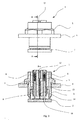
- FIGS. 1 . 2 and 3 show a female connector assembly, which is a shielded female connector 1 for printed circuit boards or boards 2, as shown in FIG. 1 is implied.
- a flange 3 is preferably arranged in a housing surface 4, wherein in the flange 3, a trained as an insulating body 5 is used, as this particular in the FIG. 7 is shown in the perspective view.
- the contact carrier 5 a plurality of conductive contacts 6 are arranged, which are shielded in pairs by means of a provided in the contact carrier 5 shielding plate 7, wherein the shielding plate 7 in particular in a single view of FIG. 6 are shown.
- the shielding plate 7 establishes a contact with the flange 3 designed as a shielding housing.
- the shielding plate 7 by means of trained as a spring strips 8 and 9 contact elements in the inserted state in the contact carrier 5 a contacting both in the radial direction, as in the FIG. 2 and 10 is shown as well as in axial alignment, shown in the FIG. 3 and 9 , to the inner wall of the flange 3.
- the shield plate 7 consists of two metal strips 10 and 11, wherein on the one sheet metal strip 10 two spring strips acting for axial alignment 8 and the other second metal strip 11 two spring strips 9 are provided for radial alignment. This situation is particularly evident in the FIG. 6 where the spring strips 8 and 9 are aligned to recognize.
- FIG. 6 shows how the two sheet metal parts 10 and 11 are inserted into each other like a cross.
- the channels 12 and 13 are also in the Bottom view in the FIG. 8 to recognize where the sheet metal parts 10 and 11 can be seen in the channels 12 and 13.
- From the FIG. 7 is also clearly seen that arranged on the sheet metal parts 10 and 11 spring strips 8 and 9 in the inserted state - FIG. 7 -
- the sheet metal parts 10 and 11 on the circumference of the contact carrier 5 extend.
- the two sheet metal parts 10 and 11 from the surface 17 protruding notches 18, which engage behind a molded undercut 19 in the channels 12 and 13 in the inserted state of the assembled sheet metal parts 10 and 11.
- This situation is particular in the FIG. 3 to recognize where the detents 18, as in the FIGS. 4 and 5 are shown, get caught on the molded undercut 19.
- embossings 21 are mounted for slit width minimization to contact points for optimization to provide the shield, wherein the flexibility of the springs in the contact area is increased by a sidecut 22 below the insertion bevels in the plate.
Landscapes
- Details Of Connecting Devices For Male And Female Coupling (AREA)
Abstract
Description
- Die Erfindung betrifft eine Steckerbuchsenanordnung umfassend eine abgeschirmte Steckerbuchse für Leiterplatten oder Platinen, die in einem Flansch oder einer anderen Gehäusegeometrie integriert ist, wobei in dem Flansch ein als Isolationskörper ausgebildeter Kontaktträger eingesetzt ist, in dem mehrere elektrisch leitende Kontakte angeordnet sind, die mittels eines im Kontaktträger vorgesehenen Abschirmbleches abgeschirmt sind, welches mittels Kontaktelementen eine Kontaktierung zum als Schirmgehäuse ausgebildeten Flansch herstellt.
- Abgeschirmte Leiterplattensteckverbinder sind insbesondere im Zusammenhang beim Einsatz von Industriebussystemen (z.B. Industrial Ethernet) in Anwendung.
- Das Steckgesicht dieser Leiterplattensteckbuchse ist im Wesentlichen festgelegt, und umfasst ein als Isolierkörper ausgebildeten Kontaktträger in dem mehrere elektrisch leitende Kontakte vorhanden sind, die mittels eines im Kontaktträger vorgesehenen Abschirmbleches optional paarweise abgeschirmt sein können.
- Das metallische Schirmgehäuse ist in üblicher Weise über mehrere Anbindungen an die Leiterplatte fest angelötet. Um die EMV (Elektromagnetische Verträglichkeit) -Richtlinien zu erfüllen, müssen die auf Leiterplatten montieren Input- / Output-Steckverbinder mit der Gehäusewand elektrisch verbunden werden. Neben der herkömmlichen Methode die Stecker unter erheblichen zusätzlichen Montageaufwand mit dem Gehäuse zu verschrauben, ist es bekannt die Montagetoleranzen der Leiterplatten über flexible Federn auszugleichen. Diese können sowohl in der Gehäusewand als auch in dem Steckverbinder selbst integriert werden. Alternativ ist es auch bekannt, ein relativ dickwandiges Schirmblech mittels eines aufgeschraubten zusätzlichen dünnen Federbleches mit der Gehäusewand elektrisch zu verbinden.
- Bei dieser nach dem Stand der Technik bekannten Ausführungsform wird es als nachteilig angesehen, dass insbesondere ein notwendiges Toleranzspiel für die Kontaktierung der Abschirmung zwischen dem Kontaktträger in Bezug zur Leiterplatte oder Platine und dem als Schirmgehäuse ausgebildeten Flansch oft nicht gegeben ist bzw. zu gering ausfällt. So kommt es dann nicht selten vor, dass auf Grund der Einbautoleranzen Kontaktierungen der Abschirmung nicht gegeben sind, weil insbesondere diese dann, wenn sie das Toleranzspiel überschreiten, unterbrochen sind oder verschlechtert werden.
- Der Erfindung stellt sich somit das Problem, eine Steckerbuchsenanordnung, umfassend eine abgeschirmte Steckerbuchse für Leiterplatten oder Platinen derart weiter zu bilden, deren Kontaktierung für die Abschirmung größere Toleranzbereiche überbrückt.
- Die mit der Erfindung erreichten Vorteile bestehen nun darin, dass auf Grund der Anordnung der Federstreifen an dem Abschirmblech ein wesentlich größerer Toleranzbereich im als Gehäuse ausgebildeten Flasch im montierten Zustand abgegriffen werden kann. So greifen hierbei die erfindungsgemäß angeordneten Federstreifen in dem Flansch Bereiche ab, die sich axial und radial im Flanschgehäuse erstrecken, so dass das Toleranzspiel sich dadurch wesentlich flexibler gestaltet, und wobei ein sicheres Kontaktieren der Abschirmung erfüllt ist.
- Gemäß der Erfindung wird daher vorgeschlagen, dass das Abschirmblech mittels als Federstreifen ausgebildeten Kontaktelementen im eingesetzten Zustand des Kontaktträgers eine Kontaktierung sowohl in radialer Ausrichtung als in axial-Ausrichtung zum Flansch bewirkt. In der vorteilhaften Ausgestaltung besteht das Abschirmblech aus zwei Blechteilen, wobei an dem einen Blechteil wenigstens ein zur Radialausrichtung wirkender Federstreifen und an dem anderen zweiten Blechteil wenigstens ein zur Axialausrichtung wirkender Federstreifen vorgesehen ist. Dabei sind die beiden Blechteile kreuzartig ineinander steckbar ausgebildet, die in ebenfalls kreuzartig angeordneten Kanälen in den Kontaktträgern einschiebbar sind. Auf Grund dieser Ausbildung wird insbesondere der als Isolationskörper ausgebildete Kontaktträger mit den Kontaktstreifen, die am Außenumfang des Kontaktträgers angeordnet sind, für eine Abschirmung im Flansch hergerichtet.
- In Weiterbindung sind an dem einen Blechteil in Einschubrichtung weisende Federstreifen und an dem anderen Blechteil gegen die Einschubrichtung weisende Federstreifen angeordnet. Dabei legen sich die in Einschubrichtungen weisenden Federstreifen an einen im Flansch angeordneten Ringansatz axial an, wobei die gegen die Einschubrichtung weisenden Federstreifen an der Innenwand des Flansches radial anliegen. Auf Grund dieser Ausbildung wird insbesondere die radiale bzw. die axiale Kontaktierung erreicht, mit der ein großer Toleranzbereich abgegriffen wird. Hierbei sind die Federstreifen mittels angeformter Arme an den Blechteilen angeordnet, wobei die axial wirkenden Federstreifen quer zur Flächenebene des Ringansatzes ausgerichtet sind, wobei die radial wirkenden Federstreifen zur Flächenebene hin ausgerichtet sind.
- Nach einer besonders vorteilhaften Ausgestaltung der Erfindung weisen die beiden Blechteile aus der Fläche herausstehende Rasten auf, welche sich hinter eingeformten Hinterschnitten in Kanälen im eingeschobenen Zustand der zusammengesteckten Blechteile verrasten. Auf Grund dieser Ausbildung wird erreicht, dass das gesteckte Kreuz aus Abschirmblechen im Isolierkörper unlösbar festgelegt ist. In Weiterbildung weisen die Blechteile in ihren Mittelachsen jeweils Schlitze auf, die im zusammengefügten Zustand der Blechteile ineinander greifen. Am Schlitz sind Prägungen zur Schlitzbreitenminimierung angebracht, um Kontaktpunkte zur Optimierung der Schirmung zu schaffen. Die Flexibilität der Federn im Kontaktbereich wird durch eine Taillierung unterhalb der Einführungsschrägen im Blech erhöht.
- Ein Ausführungsbeispiel der Erfindung ist in den Zeichnungen rein schematisch dargestellt und wird nachfolgend näher beschrieben. Es zeigt
- Figur 1
- eine perspektivische Darstellung einer Steckerbuchsenanordnung;
- Figur 2
- eine Seitenansicht sowie eine Schnittdarstellung der Steckerbuchse gemäß der
Figur 1 in der Schnittebene A - A; - Figur 3
- eine weitere Seitenansicht sowie eine Schnittdarstellung der Steckerbuchse gemäß der
Figur 1 in der Schnittebene B - B; - Figur 4
- eine perspektivische Darstellung eines ersten Blechsteifens zur axialen Kontaktierung;
- Figur 4a
- eine weitere Darstellung gemäß der
Figur 4 mit Detailansicht; - Figur 5
- eine perspektivische Darstellung des zweiten Blechstreifens zur radialen Kontaktierung;
- Figur 5a
- eine weitere Darstellung gemäß der
Figur 5 mit Detailansicht; - Figur 6
- eine perspektivische Darstellung der Blechstreifen im zusammengesteckten Zustand;
- Figur 7
- eine perspektivische Darstellung des Kontaktträgers mit eingefügten Abschirmkreuz;
- Figur 8
- eine Ansicht von Unten auf eine Steckerbuchse gemäß der
Figur 1 ; - Figur 9
- eine weitere geschnittene Ansicht der Steckerbuchse gemäß der Schnittlinie A - A mit Ansicht der axialen Kontaktierung in
Figur 8 und - Figur 10
- eine geschnittene Ansicht der Steckerbuchse mit Ansicht der radialen Kontaktierung gemäß der Schnittlinie B - B in
Figur 8 . - Die
Figuren 1 ,2 und3 zeigen eine Steckerbuchsenanordnung, welche eine abgeschirmte Steckerbuchse 1 für Leiterplatten oder Platinen 2, wie in derFigur 1 angedeutet ist, umfasst. Dabei ist ein Flansch 3 vorzugsweise in einer Gehäusefläche 4 angeordnet, wobei in dem Flansch 3 ein als Isolierkörper ausgebildeteter Kontaktträger 5 eingesetzt ist, wie dieser insbesondere in derFigur 7 in der perspektivischen Darstellung gezeigt wird. In dem Kontaktträger 5 sind mehrere leitende Kontakte 6 angeordnet, die mittels eines im Kontaktträger 5 vorgesehenen Abschirmbleches 7 paarweise abgeschirmt sind, wobei das Abschirmblech 7 insbesondere in Einzelansicht derFigur 6 gezeigt sind. Das Abschirmblech 7 stellt hierbei eine Kontaktierung zum als Abschirmgehäuse ausgebildeten Flansch 3 her. - Aus der Zusammenschau der
Figuren 2 und3 aber auch 9 und 10 bewirkt das Abschirmblech 7 mittels der als Federstreifen 8 und 9 ausgebildeten Kontaktelemente im eingesetzten Zustand im Kontaktträger 5 eine Kontaktierung sowohl in radialer Richtung, wie in derFigur 2 und10 dargestellt ist, als auch in Axialausrichtung, dargestellt in derFigur 3 und9 , zur Innenwand des Flansches 3. Wie insbesondere weiter aus der Zusammenschau derFiguren 4, 5 und 6 erkennbar ist, besteht das Abschirmblech 7 aus zwei Blechstreifen 10 und 11, wobei an dem einen Blechstreifen 10 zwei zur Axialausrichtung wirkende Federstreifen 8 und an dem anderen zweiten Blechstreifen 11 zwei Federstreifen 9 zur Radialausrichtung vorgesehen sind. Diese Situation ist insbesondere gut zu erkennen in derFigur 6 , wo die Federstreifen 8 und 9 entsprechend ausgerichtet zu erkennen sind. DieFigur 6 zeigt wie die beiden Blechteile 10 und 11 kreuzartig ineinander gesteckt sind. In derFigur 7 und 8 sind die kreuzartig angeordneten Blechteile 10 und 11 in im Kontaktträger eingeformte Kanäle 12 und 13 eingeschoben, wie dies insbesondere in derFigur 7 deutlich zu erkennen ist. Die Kanäle 12 und 13 sind ebenfalls in der Ansicht von unten in derFigur 8 zu erkennen, wo die Blechteile 10 und 11 in den Kanälen 12 und 13 zu erkennen sind. Aus derFigur 7 ist auch deutlich zu sehen, dass die an den Blechteilen 10 und 11 angeordneten Federstreifen 8 und 9 sich im eingeschobenen Zustand -Figur 7 - der Blechteile 10 und 11 am Umfang des Kontaktträgers 5 erstrecken. - Dabei sind - wie insbesondere aus der
Figur 7 ersichtlich - an dem einen Blechteil 10 in Einschubrichtung weisende Federstreifen 8 und an dem anderen Blechteil 11 gegen die Einschubrichtung weisende Federstreifen 9 angeordnet, um auf diese Weise die radiale und axiale Ausrichtung der Federstreifen 8 und 9 zu bewirkten. Dabei sind die Federstreifen 8 und 9 mittels angeformter Arme 14 an den Blechteilen 10 und 11 angeordnet, wobei die axial wirkenden Federstreifen 8 quer zur Flächenebene und die radial wirkenden Federstreifen 9 zur Flächenebene hin ausgerichtet sind. Auf Grund dieser Ausbildung ergibt sich, dass die in Einschubrichtung weisenden Federstreifen 8 an einem im Flansch angeordneten Ringansatz 15 anliegen, wobei die gegen die Einschubrichtung weisenden Federstreifen 9 an der Innenwand 16 des Flansches 3 anliegen, wie dies insbesondere aus der Zusammenschau derFiguren 9 und 10 ersichtlich ist. - Nach einer besonders vorteilhaften Weiterbildung der Erfindung weisen die beiden Blechteile 10 und 11 aus der Fläche 17 herausstehende Rasten 18 auf, welche sich hinter einem eingeformten Hinterschnitt 19 in den Kanälen 12 und 13 im eingeschobenen Zustand der zusammengesteckten Blechteile 10 und 11 verrasten. Diese Situation ist insbesondere in der
Figur 3 zu erkennen, wo die Rasten 18, wie sie in derFigur 4 und 5 gezeigt sind, sich an den eingeformten Hinterschnitt 19 verhaken. Wie insbesondere noch aus denFiguren 4 und 5 zu erkennen ist, weisen die zusammensteckbaren Blechteile 10 und 11 in der Mittelachse jeweils Schlitze 20 auf, die die Flächenbereiche des jeweiligen Blechteils 10, 11 im zusammengesteckten Zustand aufnehmen. - Aus den
Figuren 4a und 5a erkennt man, dass am Schlitz 20 Prägungen 21 zur Schlitzbreitenminimierung angebracht sind, um Kontaktpunkte zur Optimierung der Schirmung zu schaffen, wobei die Flexibilität der Federn im Kontaktbereich durch eine Taillierung 22 unterhalb der Einführungsschrägen im Blech erhöht wird. -
- 01
- Steckerbuchse
- 02
- Leiterplatten oder Platinen
- 03
- Flansch
- 04
- Gehäusefläche
- 05
- Kontaktträger
- 06
- Kontakte
- 07
- Abschirmblech
- 08
- Federstreifen axial
- 09
- Federstreifen radial
- 10
- Blechteil axial
- 11
- Blechteil radial
- 12
- Kanal
- 13
- Kanal
- 14
- Arme
- 15
- Ringansatz
- 16
- Innenwand Flansch
- 17
- Fläche Blechteil
- 18
- Rasten
- 19
- Hinterschnitt
- 20
- Schlitze
- 21
- Prägungen
- 22
- Taillierung
Claims (10)
- Steckerbuchsenanordnung, umfassend eine abgeschirmte Steckerbuchse (1) für Leiterplatten oder Platinen (2), die in einem Flansch (3) oder einer anderen Gehäusegeometrie (4) integriert ist, wobei in dem Flansch (3) ein als Isolationskörper ausgebildeter Kontaktträger (5) eingesetzt ist, in dem mehrere elektrisch leitende Kontakte (6) angeordnet sind, die mittels eines im Kontaktträger (5) vorgesehenen Abschirmbleches (7) abgeschirmt sind, welches mittels Kontaktelementen eine Kontaktierung zum als Schirmgehäuse ausgebildeten Flansch (3) herstellt,
dadurch gekennzeichnet,
dass das Abschirmblech (7) mittels als Federstreifen (8) und (9) ausgebildeten Kontaktelementen im eingesetzten Zustand im Kontaktträger (5) eine Kontaktierung sowohl in Radialausrichtung als auch in Axialausrichtung zum Flansch (3) bewirkt. - Steckerbuchenanordnung nach Anspruch 1,
dadurch gekennzeichnet,
dass das Abschirmblech (7) aus einem oder mehreren Blechteilen (10) und (11) besteht, wobei an dem einen Blechteil (11) wenigstens ein zur Radialausrichtung wirkender Federstreifen (9) und an dem anderen zweiten Blechteil (10) wenigstes ein zur Axialausrichtung wirkender Federstreifen (8) vorgesehen ist. - Steckerbuchenanordnung nach Anspruch 2,
dadurch gekennzeichnet,
dass die beiden Blechteile (10) und (11) kreuzartig ineinander steckbar ausgebildet sind, die in ebenfalls kreuzartig angeordneten Kanälen (12) und (13) in den Kontaktträger (5) einschiebbar sind, wobei angeformte Prägungen (21) für ein besseres Schirmverhalten vorgesehen sind. - Steckerbuchenanordnung nach Anspruch 3,
dadurch gekennzeichnet,
dass die an den Blechteilen (10) und (11) angeordneten Federstreifen (8) und (9) sich im eingeschobenen Zustand der Blechteile (10) und (11) am Umfang des Kontaktträgers (5) erstrecken. - Steckerbuchenanordnung nach Anspruch 4,
dadurch gekennzeichnet,
dass an dem einen Blechteil (10) in Einschubrichtung weisende Federstreifen (8) und an dem anderen Blechteil (11) gegen die Einschubrichtung weisende Federstreifen (9) angeordnet sind. - Steckerbuchenanordnung nach Anspruch 5,
dadurch gekennzeichnet,
dass die in Einschubrichtung weisenden Federstreifen (8) sich an einen im Flansch (3) angeordneten Ringansatz (15) oder an einer anderen Gehäusegeometrie anlegen, wobei die gegen die Einschubrichtung weisenden Federstreifen (9) sich an der Innenwand (16) des Flansches (3) anlegen. - Steckerbuchenanordnung nach Anspruch 6,
dadurch gekennzeichnet,
dass die Federstreifen (8) und (9) mittels angeformter Arme (14) an den Blechteilen (10) und (11) angeordnet sind, wobei die axial wirkenden Federstreifen (8) quer zur Flächenebene und die radial wirkenden Federstreifen (9) zur Flächenebene hin ausgerichtet sind. - Steckerbuchenanordnung nach Anspruch 1 bis 7,
dadurch gekennzeichnet,
dass die beiden Blechteile (10) und (11) aus der Fläche (17) herausstehende Rasten (18) aufweisen, welche sich hinter eingeformten Hinterschnitten (19) in den Kanälen (12) und (13) im eingeschobenen Zustand der zusammengesteckten Blechteile (10) und (11) verrasten. - Steckerbuchenanordnung nach Anspruch 8,
dadurch gekennzeichnet,
dass die zusammensteckbaren Blechteile (10) und (11) in den Mittelachsen jeweils Schlitze (20) aufweisen, die die Flächbereiche des jeweiligen Blechteils (10), (11) im zusammengesteckten Zustand aufnehmen. - Steckerbuchenanordnung nach Anspruch 8 und 9,
dadurch gekennzeichnet,
dass im Steckbereich der Blechteile (10) und (11) Taillierungen (22) vorgesehen sind.
Applications Claiming Priority (1)
| Application Number | Priority Date | Filing Date | Title |
|---|---|---|---|
| DE202015100245.9U DE202015100245U1 (de) | 2015-01-21 | 2015-01-21 | Steckerbuchsenanordnung umfassend eine abgeschirmte Steckerbuchse für Leiterplatten oder Platinen |
Publications (2)
| Publication Number | Publication Date |
|---|---|
| EP3048675A1 true EP3048675A1 (de) | 2016-07-27 |
| EP3048675B1 EP3048675B1 (de) | 2019-01-02 |
Family
ID=55221332
Family Applications (1)
| Application Number | Title | Priority Date | Filing Date |
|---|---|---|---|
| EP16152279.2A Active EP3048675B1 (de) | 2015-01-21 | 2016-01-21 | Steckerbuchsenanordnung umfassend eine abgeschirmte steckerbuchse für leiterplatten oder platinen |
Country Status (2)
| Country | Link |
|---|---|
| EP (1) | EP3048675B1 (de) |
| DE (1) | DE202015100245U1 (de) |
Cited By (2)
| Publication number | Priority date | Publication date | Assignee | Title |
|---|---|---|---|---|
| WO2019072336A1 (de) * | 2017-10-10 | 2019-04-18 | HARTING Electronics GmbH | Leiterkartensteckverbinder mit einem schirmelement |
| CN111758189A (zh) * | 2018-02-19 | 2020-10-09 | 哈廷电子有限公司及两合公司 | 带有屏蔽连接元件的印刷电路板插接连接器 |
Families Citing this family (7)
| Publication number | Priority date | Publication date | Assignee | Title |
|---|---|---|---|---|
| CN105633733A (zh) * | 2016-03-11 | 2016-06-01 | 镇江科茂电子有限公司 | 一种简易射频连接器 |
| DE102018202939B4 (de) * | 2018-02-27 | 2019-12-05 | Robert Bosch Gmbh | Stecker zur Aufnahme von elektrischen Leitungen |
| CN113078491B (zh) * | 2021-03-08 | 2023-04-18 | 中航光电科技股份有限公司 | 一种浮动连接器及导电结构 |
| US12199385B2 (en) | 2022-04-29 | 2025-01-14 | Te Connectivity Solutions Gmbh | High speed cable braid termination using a coil spring |
| US12244104B2 (en) | 2022-04-29 | 2025-03-04 | Te Connectivity Solutions Gmbh | High speed electrical connector with preassembled EMI shielding |
| US12244105B2 (en) | 2022-04-29 | 2025-03-04 | Te Connectivity Solutions Gmbh | Isolation component for a tightly packaged high speed connector |
| US12266880B2 (en) | 2022-04-29 | 2025-04-01 | Te Connectivity Solutions Gmbh | Contact insulators for use with differential pairs of contacts and method of termination |
Citations (7)
| Publication number | Priority date | Publication date | Assignee | Title |
|---|---|---|---|---|
| US5035650A (en) * | 1990-06-15 | 1991-07-30 | Amp Incorporated | Electrical connector having an inner metal shield |
| DE102004018103B3 (de) * | 2004-04-14 | 2005-09-08 | U.I. Lapp Gmbh | Verbinder für signalübertragende Kabel |
| FR2921522A1 (fr) * | 2007-09-20 | 2009-03-27 | Souriau Soc Par Actions Simpli | Connecteur pour cables ethernet et kit pour connecteur |
| DE102010051954B3 (de) * | 2010-08-13 | 2012-02-09 | Harting Electronics Gmbh & Co. Kg | Steckverbinder für differenzielle Datenübertragung |
| DE102011052792A1 (de) * | 2011-08-18 | 2013-02-21 | Harting Electronics Gmbh & Co. Kg | Isolierkörper mit Schirmkreuz |
| DE102012105257A1 (de) * | 2012-06-18 | 2013-12-19 | HARTING Electronics GmbH | Isolierkörper eines Steckverbinders |
| DE202014105530U1 (de) * | 2014-11-18 | 2014-12-09 | Phoenix Contact Gmbh & Co. Kg | Steckverbinder |
Family Cites Families (5)
| Publication number | Priority date | Publication date | Assignee | Title |
|---|---|---|---|---|
| JPH0531824Y2 (de) * | 1985-06-07 | 1993-08-16 | ||
| JPH0298074A (ja) * | 1988-10-04 | 1990-04-10 | Hirose Electric Co Ltd | 電気コネクタ |
| US5017158A (en) * | 1990-05-02 | 1991-05-21 | Pan-International Industrial Corp. | Structure of receptacle for electric connector with self-locking and electric shield mechanism |
| US7568950B2 (en) * | 2006-05-17 | 2009-08-04 | Bel Fuse Ltd. | High speed modular jack including multiple contact blocks and method for assembling same |
| JP2013229139A (ja) * | 2012-04-24 | 2013-11-07 | Yazaki Corp | 機器直付用シールドコネクタ |
-
2015
- 2015-01-21 DE DE202015100245.9U patent/DE202015100245U1/de not_active Expired - Lifetime
-
2016
- 2016-01-21 EP EP16152279.2A patent/EP3048675B1/de active Active
Patent Citations (7)
| Publication number | Priority date | Publication date | Assignee | Title |
|---|---|---|---|---|
| US5035650A (en) * | 1990-06-15 | 1991-07-30 | Amp Incorporated | Electrical connector having an inner metal shield |
| DE102004018103B3 (de) * | 2004-04-14 | 2005-09-08 | U.I. Lapp Gmbh | Verbinder für signalübertragende Kabel |
| FR2921522A1 (fr) * | 2007-09-20 | 2009-03-27 | Souriau Soc Par Actions Simpli | Connecteur pour cables ethernet et kit pour connecteur |
| DE102010051954B3 (de) * | 2010-08-13 | 2012-02-09 | Harting Electronics Gmbh & Co. Kg | Steckverbinder für differenzielle Datenübertragung |
| DE102011052792A1 (de) * | 2011-08-18 | 2013-02-21 | Harting Electronics Gmbh & Co. Kg | Isolierkörper mit Schirmkreuz |
| DE102012105257A1 (de) * | 2012-06-18 | 2013-12-19 | HARTING Electronics GmbH | Isolierkörper eines Steckverbinders |
| DE202014105530U1 (de) * | 2014-11-18 | 2014-12-09 | Phoenix Contact Gmbh & Co. Kg | Steckverbinder |
Cited By (5)
| Publication number | Priority date | Publication date | Assignee | Title |
|---|---|---|---|---|
| WO2019072336A1 (de) * | 2017-10-10 | 2019-04-18 | HARTING Electronics GmbH | Leiterkartensteckverbinder mit einem schirmelement |
| KR20200054325A (ko) * | 2017-10-10 | 2020-05-19 | 하르팅 에렉트로닉스 게엠베하 | 차폐 요소를 포함한 인쇄회로기판 커넥터 |
| US10763623B2 (en) | 2017-10-10 | 2020-09-01 | HARTING Electronics GmbH | Printed circuit board connector having a shielding element |
| CN111758189A (zh) * | 2018-02-19 | 2020-10-09 | 哈廷电子有限公司及两合公司 | 带有屏蔽连接元件的印刷电路板插接连接器 |
| CN111758189B (zh) * | 2018-02-19 | 2022-04-26 | 哈廷电子有限公司及两合公司 | 带有屏蔽连接元件的印刷电路板插接连接器 |
Also Published As
| Publication number | Publication date |
|---|---|
| EP3048675B1 (de) | 2019-01-02 |
| DE202015100245U1 (de) | 2016-02-02 |
Similar Documents
| Publication | Publication Date | Title |
|---|---|---|
| EP3048675B1 (de) | Steckerbuchsenanordnung umfassend eine abgeschirmte steckerbuchse für leiterplatten oder platinen | |
| DE102014201398B4 (de) | Dichtungsglied und Dichtungsaufbau | |
| DE102010028672B4 (de) | Steckverbindung mit Spielausgleichseinrichtung | |
| EP3400631A1 (de) | Halterahmen für einen steckverbinder und verfahren zur bestückung | |
| EP2950395A1 (de) | Federkranz für eine abschirmung von elektrischen steckverbindern | |
| DE102015120921B4 (de) | Steckverbinder und Steckerverbinderanordnung | |
| DE102017105186B4 (de) | Rundsteckverbinderbuchse für eine daran anordenbare Leiterplatte | |
| DE102014221970A1 (de) | Stifteinheit für ein Verbindergehäuse und Verbindergehäuse hiermit | |
| EP3895256B1 (de) | Rundsteckverbinder mit verriegelung | |
| EP3178135A1 (de) | Halterahmen und verfahren zu seiner herstellung | |
| DE112017001259B4 (de) | Tragschienenbaugruppe mit einem Bussystem und einem eine Leiterplatte aufweisenden Elektronikgerät | |
| DE102020132246A1 (de) | Schwebender Verbinder und Kabelbaumträger | |
| DE112012002772T5 (de) | Hebelartiger Steckverbinder | |
| EP3396785A1 (de) | Steckeranordnung | |
| DE202017101396U1 (de) | Rundsteckverbinderbuchse für eine daran anordenbare Leiterplatte | |
| DE102016220022B4 (de) | Kombination eines Steckers mit einem Deckel | |
| DE102016211300A1 (de) | Halterahmen für einen Steckverbinder und Verfahren zur Bestückung | |
| DE112013002643T5 (de) | Steckverbinder des Hebeltyps | |
| DE102018107886B4 (de) | Steckverbindersystem mit einem bistabilen Element | |
| DE202015009096U1 (de) | Rundsteckverbinder mit Toleranzausgleichmittel | |
| DE102010025385B4 (de) | Geschirmter Steckverbinder | |
| DE202018006450U1 (de) | Steckverbinder zur Herstellung elektrisch leitender Verbindungen | |
| DE102012105901A1 (de) | Zugentlastungseinheit für einen elektrischen Steckverbinder und Gerätegehäuse | |
| DE102019207091B4 (de) | Steckverbinder | |
| DE102018128089B4 (de) | Steckverbinder zur Herstellung elektrisch leitender Verbindungen |
Legal Events
| Date | Code | Title | Description |
|---|---|---|---|
| PUAI | Public reference made under article 153(3) epc to a published international application that has entered the european phase |
Free format text: ORIGINAL CODE: 0009012 |
|
| AK | Designated contracting states |
Kind code of ref document: A1 Designated state(s): AL AT BE BG CH CY CZ DE DK EE ES FI FR GB GR HR HU IE IS IT LI LT LU LV MC MK MT NL NO PL PT RO RS SE SI SK SM TR |
|
| AX | Request for extension of the european patent |
Extension state: BA ME |
|
| STAA | Information on the status of an ep patent application or granted ep patent |
Free format text: STATUS: REQUEST FOR EXAMINATION WAS MADE |
|
| 17P | Request for examination filed |
Effective date: 20170125 |
|
| RBV | Designated contracting states (corrected) |
Designated state(s): AL AT BE BG CH CY CZ DE DK EE ES FI FR GB GR HR HU IE IS IT LI LT LU LV MC MK MT NL NO PL PT RO RS SE SI SK SM TR |
|
| STAA | Information on the status of an ep patent application or granted ep patent |
Free format text: STATUS: EXAMINATION IS IN PROGRESS |
|
| 17Q | First examination report despatched |
Effective date: 20180112 |
|
| GRAP | Despatch of communication of intention to grant a patent |
Free format text: ORIGINAL CODE: EPIDOSNIGR1 |
|
| STAA | Information on the status of an ep patent application or granted ep patent |
Free format text: STATUS: GRANT OF PATENT IS INTENDED |
|
| RIC1 | Information provided on ipc code assigned before grant |
Ipc: H01R 12/91 20110101ALN20180517BHEP Ipc: H01R 24/86 20110101ALN20180517BHEP Ipc: H01R 13/6594 20110101ALI20180517BHEP Ipc: H01R 13/6585 20110101AFI20180517BHEP Ipc: H01R 13/74 20060101ALN20180517BHEP Ipc: H01R 12/58 20110101ALN20180517BHEP Ipc: H01R 13/502 20060101ALI20180517BHEP |
|
| INTG | Intention to grant announced |
Effective date: 20180619 |
|
| GRAJ | Information related to disapproval of communication of intention to grant by the applicant or resumption of examination proceedings by the epo deleted |
Free format text: ORIGINAL CODE: EPIDOSDIGR1 |
|
| GRAP | Despatch of communication of intention to grant a patent |
Free format text: ORIGINAL CODE: EPIDOSNIGR1 |
|
| INTG | Intention to grant announced |
Effective date: 20180810 |
|
| GRAJ | Information related to disapproval of communication of intention to grant by the applicant or resumption of examination proceedings by the epo deleted |
Free format text: ORIGINAL CODE: EPIDOSDIGR1 |
|
| STAA | Information on the status of an ep patent application or granted ep patent |
Free format text: STATUS: EXAMINATION IS IN PROGRESS |
|
| GRAP | Despatch of communication of intention to grant a patent |
Free format text: ORIGINAL CODE: EPIDOSNIGR1 |
|
| STAA | Information on the status of an ep patent application or granted ep patent |
Free format text: STATUS: GRANT OF PATENT IS INTENDED |
|
| INTC | Intention to grant announced (deleted) | ||
| INTG | Intention to grant announced |
Effective date: 20181005 |
|
| RIC1 | Information provided on ipc code assigned before grant |
Ipc: H01R 24/86 20110101ALN20180924BHEP Ipc: H01R 13/502 20060101ALI20180924BHEP Ipc: H01R 12/58 20110101ALN20180924BHEP Ipc: H01R 13/6585 20110101AFI20180924BHEP Ipc: H01R 13/74 20060101ALN20180924BHEP Ipc: H01R 12/91 20110101ALN20180924BHEP Ipc: H01R 13/6594 20110101ALI20180924BHEP |
|
| GRAS | Grant fee paid |
Free format text: ORIGINAL CODE: EPIDOSNIGR3 |
|
| GRAA | (expected) grant |
Free format text: ORIGINAL CODE: 0009210 |
|
| STAA | Information on the status of an ep patent application or granted ep patent |
Free format text: STATUS: THE PATENT HAS BEEN GRANTED |
|
| AK | Designated contracting states |
Kind code of ref document: B1 Designated state(s): AL AT BE BG CH CY CZ DE DK EE ES FI FR GB GR HR HU IE IS IT LI LT LU LV MC MK MT NL NO PL PT RO RS SE SI SK SM TR |
|
| REG | Reference to a national code |
Ref country code: GB Ref legal event code: FG4D Free format text: NOT ENGLISH |
|
| REG | Reference to a national code |
Ref country code: CH Ref legal event code: EP Ref country code: AT Ref legal event code: REF Ref document number: 1085608 Country of ref document: AT Kind code of ref document: T Effective date: 20190115 |
|
| REG | Reference to a national code |
Ref country code: IE Ref legal event code: FG4D Free format text: LANGUAGE OF EP DOCUMENT: GERMAN |
|
| REG | Reference to a national code |
Ref country code: DE Ref legal event code: R096 Ref document number: 502016003022 Country of ref document: DE |
|
| REG | Reference to a national code |
Ref country code: NL Ref legal event code: MP Effective date: 20190102 |
|
| REG | Reference to a national code |
Ref country code: LT Ref legal event code: MG4D |
|
| PG25 | Lapsed in a contracting state [announced via postgrant information from national office to epo] |
Ref country code: NL Free format text: LAPSE BECAUSE OF FAILURE TO SUBMIT A TRANSLATION OF THE DESCRIPTION OR TO PAY THE FEE WITHIN THE PRESCRIBED TIME-LIMIT Effective date: 20190102 |
|
| PG25 | Lapsed in a contracting state [announced via postgrant information from national office to epo] |
Ref country code: FI Free format text: LAPSE BECAUSE OF FAILURE TO SUBMIT A TRANSLATION OF THE DESCRIPTION OR TO PAY THE FEE WITHIN THE PRESCRIBED TIME-LIMIT Effective date: 20190102 Ref country code: PT Free format text: LAPSE BECAUSE OF FAILURE TO SUBMIT A TRANSLATION OF THE DESCRIPTION OR TO PAY THE FEE WITHIN THE PRESCRIBED TIME-LIMIT Effective date: 20190502 Ref country code: SE Free format text: LAPSE BECAUSE OF FAILURE TO SUBMIT A TRANSLATION OF THE DESCRIPTION OR TO PAY THE FEE WITHIN THE PRESCRIBED TIME-LIMIT Effective date: 20190102 Ref country code: NO Free format text: LAPSE BECAUSE OF FAILURE TO SUBMIT A TRANSLATION OF THE DESCRIPTION OR TO PAY THE FEE WITHIN THE PRESCRIBED TIME-LIMIT Effective date: 20190402 Ref country code: PL Free format text: LAPSE BECAUSE OF FAILURE TO SUBMIT A TRANSLATION OF THE DESCRIPTION OR TO PAY THE FEE WITHIN THE PRESCRIBED TIME-LIMIT Effective date: 20190102 Ref country code: LT Free format text: LAPSE BECAUSE OF FAILURE TO SUBMIT A TRANSLATION OF THE DESCRIPTION OR TO PAY THE FEE WITHIN THE PRESCRIBED TIME-LIMIT Effective date: 20190102 Ref country code: ES Free format text: LAPSE BECAUSE OF FAILURE TO SUBMIT A TRANSLATION OF THE DESCRIPTION OR TO PAY THE FEE WITHIN THE PRESCRIBED TIME-LIMIT Effective date: 20190102 |
|
| PG25 | Lapsed in a contracting state [announced via postgrant information from national office to epo] |
Ref country code: HR Free format text: LAPSE BECAUSE OF FAILURE TO SUBMIT A TRANSLATION OF THE DESCRIPTION OR TO PAY THE FEE WITHIN THE PRESCRIBED TIME-LIMIT Effective date: 20190102 Ref country code: RS Free format text: LAPSE BECAUSE OF FAILURE TO SUBMIT A TRANSLATION OF THE DESCRIPTION OR TO PAY THE FEE WITHIN THE PRESCRIBED TIME-LIMIT Effective date: 20190102 Ref country code: BG Free format text: LAPSE BECAUSE OF FAILURE TO SUBMIT A TRANSLATION OF THE DESCRIPTION OR TO PAY THE FEE WITHIN THE PRESCRIBED TIME-LIMIT Effective date: 20190402 Ref country code: GR Free format text: LAPSE BECAUSE OF FAILURE TO SUBMIT A TRANSLATION OF THE DESCRIPTION OR TO PAY THE FEE WITHIN THE PRESCRIBED TIME-LIMIT Effective date: 20190403 Ref country code: LV Free format text: LAPSE BECAUSE OF FAILURE TO SUBMIT A TRANSLATION OF THE DESCRIPTION OR TO PAY THE FEE WITHIN THE PRESCRIBED TIME-LIMIT Effective date: 20190102 Ref country code: IS Free format text: LAPSE BECAUSE OF FAILURE TO SUBMIT A TRANSLATION OF THE DESCRIPTION OR TO PAY THE FEE WITHIN THE PRESCRIBED TIME-LIMIT Effective date: 20190502 |
|
| REG | Reference to a national code |
Ref country code: CH Ref legal event code: PL |
|
| PG25 | Lapsed in a contracting state [announced via postgrant information from national office to epo] |
Ref country code: LU Free format text: LAPSE BECAUSE OF NON-PAYMENT OF DUE FEES Effective date: 20190121 |
|
| REG | Reference to a national code |
Ref country code: DE Ref legal event code: R097 Ref document number: 502016003022 Country of ref document: DE |
|
| REG | Reference to a national code |
Ref country code: BE Ref legal event code: MM Effective date: 20190131 |
|
| REG | Reference to a national code |
Ref country code: IE Ref legal event code: MM4A |
|
| PG25 | Lapsed in a contracting state [announced via postgrant information from national office to epo] |
Ref country code: EE Free format text: LAPSE BECAUSE OF FAILURE TO SUBMIT A TRANSLATION OF THE DESCRIPTION OR TO PAY THE FEE WITHIN THE PRESCRIBED TIME-LIMIT Effective date: 20190102 Ref country code: SK Free format text: LAPSE BECAUSE OF FAILURE TO SUBMIT A TRANSLATION OF THE DESCRIPTION OR TO PAY THE FEE WITHIN THE PRESCRIBED TIME-LIMIT Effective date: 20190102 Ref country code: IT Free format text: LAPSE BECAUSE OF FAILURE TO SUBMIT A TRANSLATION OF THE DESCRIPTION OR TO PAY THE FEE WITHIN THE PRESCRIBED TIME-LIMIT Effective date: 20190102 Ref country code: DK Free format text: LAPSE BECAUSE OF FAILURE TO SUBMIT A TRANSLATION OF THE DESCRIPTION OR TO PAY THE FEE WITHIN THE PRESCRIBED TIME-LIMIT Effective date: 20190102 Ref country code: MC Free format text: LAPSE BECAUSE OF FAILURE TO SUBMIT A TRANSLATION OF THE DESCRIPTION OR TO PAY THE FEE WITHIN THE PRESCRIBED TIME-LIMIT Effective date: 20190102 Ref country code: CZ Free format text: LAPSE BECAUSE OF FAILURE TO SUBMIT A TRANSLATION OF THE DESCRIPTION OR TO PAY THE FEE WITHIN THE PRESCRIBED TIME-LIMIT Effective date: 20190102 Ref country code: AL Free format text: LAPSE BECAUSE OF FAILURE TO SUBMIT A TRANSLATION OF THE DESCRIPTION OR TO PAY THE FEE WITHIN THE PRESCRIBED TIME-LIMIT Effective date: 20190102 Ref country code: RO Free format text: LAPSE BECAUSE OF FAILURE TO SUBMIT A TRANSLATION OF THE DESCRIPTION OR TO PAY THE FEE WITHIN THE PRESCRIBED TIME-LIMIT Effective date: 20190102 |
|
| PLBE | No opposition filed within time limit |
Free format text: ORIGINAL CODE: 0009261 |
|
| STAA | Information on the status of an ep patent application or granted ep patent |
Free format text: STATUS: NO OPPOSITION FILED WITHIN TIME LIMIT |
|
| PG25 | Lapsed in a contracting state [announced via postgrant information from national office to epo] |
Ref country code: SM Free format text: LAPSE BECAUSE OF FAILURE TO SUBMIT A TRANSLATION OF THE DESCRIPTION OR TO PAY THE FEE WITHIN THE PRESCRIBED TIME-LIMIT Effective date: 20190102 Ref country code: BE Free format text: LAPSE BECAUSE OF NON-PAYMENT OF DUE FEES Effective date: 20190131 |
|
| 26N | No opposition filed |
Effective date: 20191003 |
|
| PG25 | Lapsed in a contracting state [announced via postgrant information from national office to epo] |
Ref country code: LI Free format text: LAPSE BECAUSE OF NON-PAYMENT OF DUE FEES Effective date: 20190131 Ref country code: CH Free format text: LAPSE BECAUSE OF NON-PAYMENT OF DUE FEES Effective date: 20190131 |
|
| PG25 | Lapsed in a contracting state [announced via postgrant information from national office to epo] |
Ref country code: IE Free format text: LAPSE BECAUSE OF NON-PAYMENT OF DUE FEES Effective date: 20190121 |
|
| PG25 | Lapsed in a contracting state [announced via postgrant information from national office to epo] |
Ref country code: FR Free format text: LAPSE BECAUSE OF NON-PAYMENT OF DUE FEES Effective date: 20190302 Ref country code: SI Free format text: LAPSE BECAUSE OF FAILURE TO SUBMIT A TRANSLATION OF THE DESCRIPTION OR TO PAY THE FEE WITHIN THE PRESCRIBED TIME-LIMIT Effective date: 20190102 |
|
| PG25 | Lapsed in a contracting state [announced via postgrant information from national office to epo] |
Ref country code: TR Free format text: LAPSE BECAUSE OF FAILURE TO SUBMIT A TRANSLATION OF THE DESCRIPTION OR TO PAY THE FEE WITHIN THE PRESCRIBED TIME-LIMIT Effective date: 20190102 |
|
| REG | Reference to a national code |
Ref country code: DE Ref legal event code: R082 Ref document number: 502016003022 Country of ref document: DE Representative=s name: PATENT- & RECHTSANWAELTE BAUER WAGNER PRIESMEY, DE Ref country code: DE Ref legal event code: R081 Ref document number: 502016003022 Country of ref document: DE Owner name: CONEC - ELEKTRONISCHE BAUELEMENTE GMBH, DE Free format text: FORMER OWNER: FILTEC GMBH FILTERTECHNOLOGIE FUER DIE ELEKTRONIKINDUSTRIE, 59557 LIPPSTADT, DE |
|
| PG25 | Lapsed in a contracting state [announced via postgrant information from national office to epo] |
Ref country code: MT Free format text: LAPSE BECAUSE OF FAILURE TO SUBMIT A TRANSLATION OF THE DESCRIPTION OR TO PAY THE FEE WITHIN THE PRESCRIBED TIME-LIMIT Effective date: 20190102 |
|
| GBPC | Gb: european patent ceased through non-payment of renewal fee |
Effective date: 20200121 |
|
| PG25 | Lapsed in a contracting state [announced via postgrant information from national office to epo] |
Ref country code: GB Free format text: LAPSE BECAUSE OF NON-PAYMENT OF DUE FEES Effective date: 20200121 |
|
| PG25 | Lapsed in a contracting state [announced via postgrant information from national office to epo] |
Ref country code: CY Free format text: LAPSE BECAUSE OF FAILURE TO SUBMIT A TRANSLATION OF THE DESCRIPTION OR TO PAY THE FEE WITHIN THE PRESCRIBED TIME-LIMIT Effective date: 20190102 |
|
| PG25 | Lapsed in a contracting state [announced via postgrant information from national office to epo] |
Ref country code: HU Free format text: LAPSE BECAUSE OF FAILURE TO SUBMIT A TRANSLATION OF THE DESCRIPTION OR TO PAY THE FEE WITHIN THE PRESCRIBED TIME-LIMIT; INVALID AB INITIO Effective date: 20160121 |
|
| REG | Reference to a national code |
Ref country code: DE Ref legal event code: R082 Ref document number: 502016003022 Country of ref document: DE Representative=s name: BAUER WAGNER PELLENGAHR SROKA PATENT- & RECHTS, DE Ref country code: DE Ref legal event code: R082 Ref document number: 502016003022 Country of ref document: DE Representative=s name: BAUER PSU PARTG MBB, DE |
|
| REG | Reference to a national code |
Ref country code: AT Ref legal event code: MM01 Ref document number: 1085608 Country of ref document: AT Kind code of ref document: T Effective date: 20210121 |
|
| PG25 | Lapsed in a contracting state [announced via postgrant information from national office to epo] |
Ref country code: AT Free format text: LAPSE BECAUSE OF NON-PAYMENT OF DUE FEES Effective date: 20210121 |
|
| PG25 | Lapsed in a contracting state [announced via postgrant information from national office to epo] |
Ref country code: MK Free format text: LAPSE BECAUSE OF FAILURE TO SUBMIT A TRANSLATION OF THE DESCRIPTION OR TO PAY THE FEE WITHIN THE PRESCRIBED TIME-LIMIT Effective date: 20190102 |
|
| P01 | Opt-out of the competence of the unified patent court (upc) registered |
Effective date: 20230519 |
|
| PGFP | Annual fee paid to national office [announced via postgrant information from national office to epo] |
Ref country code: DE Payment date: 20260131 Year of fee payment: 11 |