EP3048611B1 - Speichereinheit, speicher und steuerungsverfahren für die speichereinheit - Google Patents
Speichereinheit, speicher und steuerungsverfahren für die speichereinheit Download PDFInfo
- Publication number
- EP3048611B1 EP3048611B1 EP14856459.4A EP14856459A EP3048611B1 EP 3048611 B1 EP3048611 B1 EP 3048611B1 EP 14856459 A EP14856459 A EP 14856459A EP 3048611 B1 EP3048611 B1 EP 3048611B1
- Authority
- EP
- European Patent Office
- Prior art keywords
- port
- storage area
- drive
- drive circuit
- memory
- Prior art date
- Legal status (The legal status is an assumption and is not a legal conclusion. Google has not performed a legal analysis and makes no representation as to the accuracy of the status listed.)
- Active
Links
Images
Classifications
-
- G—PHYSICS
- G11—INFORMATION STORAGE
- G11C—STATIC STORES
- G11C19/00—Digital stores in which the information is moved stepwise, e.g. shift registers
- G11C19/02—Digital stores in which the information is moved stepwise, e.g. shift registers using magnetic elements
- G11C19/08—Digital stores in which the information is moved stepwise, e.g. shift registers using magnetic elements using thin films in plane structure
- G11C19/0808—Digital stores in which the information is moved stepwise, e.g. shift registers using magnetic elements using thin films in plane structure using magnetic domain propagation
-
- G—PHYSICS
- G11—INFORMATION STORAGE
- G11C—STATIC STORES
- G11C11/00—Digital stores characterised by the use of particular electric or magnetic storage elements; Storage elements therefor
- G11C11/02—Digital stores characterised by the use of particular electric or magnetic storage elements; Storage elements therefor using magnetic elements
- G11C11/14—Digital stores characterised by the use of particular electric or magnetic storage elements; Storage elements therefor using magnetic elements using thin-film elements
- G11C11/15—Digital stores characterised by the use of particular electric or magnetic storage elements; Storage elements therefor using magnetic elements using thin-film elements using multiple magnetic layers
-
- G—PHYSICS
- G11—INFORMATION STORAGE
- G11C—STATIC STORES
- G11C11/00—Digital stores characterised by the use of particular electric or magnetic storage elements; Storage elements therefor
- G11C11/02—Digital stores characterised by the use of particular electric or magnetic storage elements; Storage elements therefor using magnetic elements
- G11C11/16—Digital stores characterised by the use of particular electric or magnetic storage elements; Storage elements therefor using magnetic elements using elements in which the storage effect is based on magnetic spin effect
- G11C11/161—Digital stores characterised by the use of particular electric or magnetic storage elements; Storage elements therefor using magnetic elements using elements in which the storage effect is based on magnetic spin effect details concerning the memory cell structure, e.g. the layers of the ferromagnetic memory cell
-
- G—PHYSICS
- G11—INFORMATION STORAGE
- G11C—STATIC STORES
- G11C11/00—Digital stores characterised by the use of particular electric or magnetic storage elements; Storage elements therefor
- G11C11/02—Digital stores characterised by the use of particular electric or magnetic storage elements; Storage elements therefor using magnetic elements
- G11C11/16—Digital stores characterised by the use of particular electric or magnetic storage elements; Storage elements therefor using magnetic elements using elements in which the storage effect is based on magnetic spin effect
- G11C11/165—Auxiliary circuits
- G11C11/1675—Writing or programming circuits or methods
-
- G—PHYSICS
- G11—INFORMATION STORAGE
- G11C—STATIC STORES
- G11C19/00—Digital stores in which the information is moved stepwise, e.g. shift registers
- G11C19/02—Digital stores in which the information is moved stepwise, e.g. shift registers using magnetic elements
- G11C19/08—Digital stores in which the information is moved stepwise, e.g. shift registers using magnetic elements using thin films in plane structure
- G11C19/0808—Digital stores in which the information is moved stepwise, e.g. shift registers using magnetic elements using thin films in plane structure using magnetic domain propagation
- G11C19/0841—Digital stores in which the information is moved stepwise, e.g. shift registers using magnetic elements using thin films in plane structure using magnetic domain propagation using electric current
Definitions
- the present invention relates to the field of data storage technologies, and in particular, to a storage unit, a memory, and a method for controlling a storage unit.
- flash memory storage there are two data storage manners: flash memory storage and hard disk storage.
- a flash memory has a high access speed, a small capacity, and a high price.
- a hard disk has a low access speed, but has a large capacity and a low price.
- a new storage manner that is, a nanowire track Racetrack memory, which has features including high performance of a flash memory and a low cost and a high capacity of a hard disk at the same time.
- An existing nanowire track is made of magnetic materials and includes multiple magnetic areas, that is, magnetic domains, where neighboring magnetic domains are separated by a magnetic domain wall, and the multiple magnetic areas and the magnetic domain walls form a U-shaped storage track.
- a high-voltage drive circuit is disposed at two ends of the top of the track, to generate a current pulse that drives the magnetic domain walls to move, and the magnetic domain walls move along the track under an action of the current pulse, so that the magnetic domains move.
- a pair of write and read apparatuses is disposed at the bottom of the track, so as to perform read and write control on the U-shaped storage track.
- a U-shaped nanowire track includes 2N magnetic domains (N is a positive integer greater than or equal to 1)
- N is a positive integer greater than or equal to 1
- the 2N magnetic domains can store only N-bit data, and storage density is low
- a voltage applied to the high-voltage drive circuit at the two ends of the top of the track is high, and therefore, power consumption of a memory is large
- a pair of read and write apparatuses controls only two memory bars in the magnetic track, and therefore, production costs are relatively high.
- US 2008/068880 A1 discloses a memory device employing magnetic domain wall movement.
- the memory device includes a writing track and a column structure.
- the writing track forms magnetic domains that have predetermined magnetization directions.
- the column structure is formed on the writing track and includes at least one interconnecting layer and at least one storage track. This document discloses the preamble of claim 1.
- US 2010/232055 A1 discloses an information storage device that includes a magnetic structure having a buffer track and a plurality of storage tracks connected to the buffer track.
- a write/read unit is disposed on the magnetic structure, and a plurality of switching devices are respectively connected to the buffer track, the plurality of storage tracks, and the write/read unit.
- the switching devices that are respectively connected to the buffer track and the storage tracks.
- the information storage device further includes a circuit configured to supply current to at least one of the magnetic structure and the write/read unit.
- US 2009/097365 A1 discloses a magnetic layer, a method of forming the magnetic layer, an information storage device, and a method of manufacturing the information storage device.
- the information storage device may include a magnetic track having a plurality of magnetic domains, a current supply element connected to the magnetic layer and a reading/writing element.
- the magnetic track includes a hard magnetic track, and the hard magnetic track has a magnetization easy-axis extending in a direction parallel to a width of the hard magnetic track.
- the present invention provides a storage unit of claim 1, a memory of claim 4, and a method for controlling the storage unit of claim 5, to increase storage density, and reduce power consumption and production costs. Implementation manners are disclosed in the dependent claims.
- the storage unit includes more than two memory bars, which are used for storing data, and therefore increases storage density; in addition, compared with a method for controlling two memory bars by using one pair of read and write apparatuses, a method for controlling more than two memory bars by using one pair of read and write apparatuses reduces manufacturing costs; in addition, a current pulse provide by a drive circuit in the storage unit needs to drive only a magnetic domain wall in a memory bar on one side of a track to move, and therefore, a drive voltage can be reduced and power consumption can also be reduced.
- any other variants mean to cover the non-exclusive inclusion, for example, a process, method, system, product, or device that includes a list of steps or units is not necessarily limited to those steps or units, but may include other steps or units not expressly listed or inherent to such a process, method, system, product, or device.
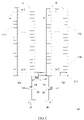
- FIG. 1 is a schematic structural diagram of a storage unit 100 according to an embodiment of the present invention, and the storage unit 100 includes: a comb-shaped magnetic track 110, a first drive circuit 20, a second drive circuit 30, a first drive port 40 connected to the first drive circuit 20, and a second drive port 50 connected to the second drive circuit 30.
- the comb-shaped magnetic track 110 includes a first storage area 111, a second storage area 112, and a comb handle 113 connected to the first storage area 111 and the second storage area 112, and at least one storage area of the first storage area 111 and the second storage area 112 includes at least two memory bars (a, b, ... shown in the figure).
- first storage area 111 is disposed between a first port A and the comb handle 113
- second storage area 112 is disposed between a second port B and the comb handle 113.
- Memory bars in the first storage area 111 and the second storage area 112 may all include N (N is a positive integer greater than or equal to 1) memory blocks, where a-1 shown in the figure is a first magnetic storage area block of a memory bar a, b-1 shown in the figure is a first magnetic storage area block of a memory bar b, a-N shown in the figure is a last magnetic storage area block of the memory bar a, and b-N shown in the figure is a last magnetic storage area block of the memory bar b.
- the first port A on the top of the comb-shaped magnetic track 110 consists of a top port of one or at least two memory bars included in the first storage area 111
- the second port B on the top of the comb-shaped magnetic track 110 consists of a top port of one or at least two memory bars included in the second storage area 112.
- both the first drive circuit 20 and the second drive circuit 30 may be designed as a transistor of a metal-oxide semiconductor (MOS, Metal Oxide Semiconductor) structure or a transistor of a CMOS structure or a drive circuit consisting of the transistor, which is not specifically limited herein.
- MOS Metal Oxide Semiconductor
- CMOS complementary metal-oxide semiconductor
- the first drive circuit 20 is configured to drive the first storage area 111
- the second drive circuit 30 is configured to drive the second storage area 112.
- a current pulse is generated in a memory bar in the first storage area 111, and a magnetic domain in the memory bar in which the current pulse is generated is driven to move.
- the first drive circuit 20 When the first drive circuit 20 is driven, and a current pulse is generated in the first storage area 111, a magnetic domain wall in the first storage area 111 is driven to move. In addition, to save energy and ensure that the first storage area 111 works properly, the second drive circuit 30 is disconnected, that is, the second drive circuit 30 does not work.
- a current pulse is generated in a memory bar in the second storage area 112, and a magnetic domain in the memory bar in which the current pulse is generated is driven to move.
- the second drive circuit 30 When the second drive circuit 30 is driven, and a current pulse is generated in the second storage area 112, a magnetic domain wall in the second storage area 112 is driven to move. In addition, to save energy and ensure that the second storage area 112 works properly, the first drive circuit 20 is disconnected, that is, the first drive circuit 20 does not work.
- the storage unit 100 provided in this embodiment of the present invention includes more than two memory bars, which are used for storing data, and therefore increases storage density; in addition, compared with a method for controlling two memory bars by using one pair of read and write apparatuses, a method of controlling more than two memory bars by using one pair of read and write apparatuses reduces manufacturing costs; in addition, a current pulse provided by a drive circuit in the storage unit 100 needs to drive only a magnetic domain wall in a memory bar on one side of a track to move, and therefore, a drive voltage can be reduced and power consumption can also be reduced.
- the first drive circuit 20 includes a first gate port 201
- the second drive circuit 30 includes a second gate port 301
- the first gate port 201 is configured to control, according to a value of a voltage applied to the first gate port 201, to switch on or off the first drive circuit 20
- the second gate port 301 is configured to control, according to a value of a voltage applied to the second gate port 301, to switch on or off the second drive circuit 30.
- a voltage difference between two ends (that is, the first drive port 40, and a top port that corresponds to a memory bar) of a memory bar (for example, the memory bar a) in the first storage area 111 is greater than or equal to a voltage threshold for driving a magnetic domain to move, a voltage difference between two ends (that is, the first drive port 40, and a top port that corresponds to a memory bar) of another memory bar in the first storage area 111 is less than the voltage threshold for driving a magnetic domain wall to move, and a voltage difference between two ends (that is, the second drive port 50, and a top port that corresponds to a memory bar) of all memory bars in the second storage area 112 is less than the voltage threshold for driving a magnetic domain wall to move, and in addition, a value of a voltage of the first gate port 201 is
- a voltage at two ends of the memory bar a in the storage unit 100 is proportional to a moving distance of a magnetic domain, that is, when a moving distance becomes longer, to maintain a same moving speed of a magnetic domain, it is required to increase the voltage at the two ends of the corresponding memory bar a.
- a voltage of each port of the storage unit 100 is controlled, so that a memory bar in the first storage area 111 and a memory bar in the second storage area 112 do not work at the same time, that is, a read operation or a write operation is controlled to be performed on only one memory bar each time.
- the storage unit 100 further includes a write circuit 60 and a read circuit 70 that are disposed at the bottom of the comb-shaped magnetic track 110, where the write circuit 60 is configured to perform a write operation on a memory bar in the first storage area 111 and a memory bar in the second storage area 112, and the read circuit 70 is configured to perform a read operation on a memory bar in the first storage area 111 and a memory bar in the second storage area 112.
- a storage principle of a memory bar in the comb-shaped magnetic track 110 is that information is stored by moving a magnetic domain.
- the first drive circuit 20 and the second drive circuit 30 are disposed at the bottom of the comb-shaped magnetic track 110 to respectively drive a magnetic domain of a memory bar in the first storage area 111 and a magnetic domain of a memory bar in the second storage area 112 to move, M ⁇ N magnetic domains in M (M is a positive integer greater than or equal to 2) memory bars can store M ⁇ N-bit data, which increases storage density.
- the storage unit 100 further includes a storage module connected to the read circuit 70, where the storage module is configured to: when a magnetic domain in any memory bar in the comb-shaped magnetic track 110 moves, store data that read out from the comb-shaped magnetic track 110.
- a current pulse may be generated in the comb-shaped magnetic track 110 (a memory bar in the first storage area 111 or a memory bar in the second storage area 112), and a magnetic domain wall is driven to move.
- Data writing is performed by using the write circuit 60 at the bottom of the track, and data reading is performed by using the read circuit 70 at the bottom of the track.
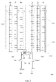
- FIG. 2 is a schematic structural diagram of the storage unit 100 provided in the application scenario. Reference may also be made to Table 1 and Table 2, where Table 1 describes port voltage control performed when the storage unit 100 performs a write operation, and Table 2 describes port voltage control performed when the storage unit 100 performs a read operation.
- the first storage area 111 consists of three memory bars, that is, a memory bar 4, a memory bar 5, and a memory bar 6, and the second storage area 112 consists of three memory bars, that is, a memory bar 1, a memory bar 2, and a memory bar 3.
- the first port A consists of a port 44, a port 55, and a port 66
- the second port B consists of a port 11, a port 22, and a port 33.
- first storage area 111 and the second storage area 112 may also consist of two, four, or more memory bars, and a quantity of memory bars of the first storage area 111 may be different from that of the second storage area 112.
- the example does not constitute a limitation on the present invention.
- control of a write operation is performed on the memory bar 1.
- the voltage Vss is applied to the second gate port 301, so that a left MOS transistor may be gated (that is, a MOS transistor in the second drive circuit 30 is switched on), and the first gate port 201 is grounded, so that a right MOS transistor is disconnected (that is, a MOS transistor in the first drive circuit 20 is switched off);
- the voltage Vpp is applied to the port 11 corresponding to the memory bar 1, and the second drive port 50 is grounded;
- a voltage at two ends of the memory bar 1 is Vpp, which is greater than the spin-transfer voltage threshold Vt2, and under driving of the second drive circuit 30, a current pulse is generated in the memory bar 1, and a magnetic domain in the memory bar 1 moves.
- a magnetic domain wall in the memory bar 1 is driven to move from the write circuit 60 and the read circuit 70 to the port 11, so as to implement a write operation.
- a voltage V-inhibit is applied to the ports 22 to 66, and a voltage at two ends of memory bars 2 to 6 is Vpp-(V-inhibit), which is less than the spin-transfer voltage threshold Vt2 and is not high enough to drive a magnetic domain wall to move. It may be understood that, a value of a voltage applied to the first drive port 40 does not affect an operation process because the right MOS transistor (that is, the MOS transistor in the first drive circuit 20) is switched off.
- the voltage of the first drive port 40 is set to be the same as a voltage of the second drive port 50 herein.
- control of a read operation is performed on the memory bar 1.
- a voltage Vss is applied to the second gate port 301, so that the left MOS transistor may be gated (that is, the MOS transistor in the second drive circuit 30 is switched on), and the first gate port 201 is grounded, so that the right MOS transistor is disconnected (that is, the MOS transistor in the first drive circuit 20 is switched off); the port 11 corresponding to the memory bar 1 is grounded, and a voltage Vpp is applied to the second drive port 50; a voltage at two ends of the memory bar 1 is Vpp, which is greater than the spin-transfer voltage threshold Vt2, and under driving of the second drive circuit 30, a current pulse is generated in the memory bar 1, and a magnetic domain in the memory bar 1 moves.
- a magnetic domain wall in the memory bar 1 is driven to move from the port 11 to the write circuit 60 and the read circuit 70, so as to implement a read operation.
- a voltage V-inhibit is applied to the ports 22 to 66, and a voltage at two ends of memory bars 2 to 6 is Vpp-(V-inhibit), which is less than the spin-transfer voltage threshold Vt2 and is not high enough to drive a magnetic domain wall to move.
- Vpp-(V-inhibit) a voltage at two ends of memory bars 2 to 6
- Vpp-(V-inhibit) which is less than the spin-transfer voltage threshold Vt2 and is not high enough to drive a magnetic domain wall to move.
- a value of a voltage applied to the first drive port 40 does not affect an operation process because the right MOS transistor (that is, the MOS transistor in the first drive circuit 20) is disconnected.
- the voltage of the first drive port 40 is set to be the same as a voltage of the first drive port 50 herein.
- a value of the voltage Vpp-(V-inhibit) is not high enough to generate a current pulse that enables a magnetic area to move, and the voltage Vpp is greater than the spin-transfer voltage threshold Vt2, and therefore, memory bars do not work at the same time by controlling a voltage of each port of the storage unit 100, that is, a read operation or a write operation is controlled to be performed on only one memory bar each time.
- the storage unit 100 provided in this embodiment of the present invention includes more than two memory bars, which are used for storing data, and therefore increases storage density; in addition, compared with a method for controlling two memory bars by using one pair of read and write apparatuses, a method for controlling more than two memory bars by using one pair of read and write apparatuses reduces manufacturing costs; in addition, a current pulse provided by a drive circuit in the storage unit 100 needs to drive only a magnetic domain wall in a memory bar on one side of a track to move, and therefore, a drive voltage can be reduced and power consumption can also be reduced.
- an embodiment of the present invention further provides a memory that is based on the foregoing storage unit 100 and a method for controlling the storage unit 100. Meanings of nouns are the same as those in the foregoing storage unit 100. For specific implementation details, reference may be made to descriptions in the foregoing embodiment.
- FIG. 3 is a schematic structural diagram of a memory 200 according to an embodiment of the present invention, where the memory 200 includes at least one storage unit 100 described above.
- the memory 200 provided in this embodiment of the present invention includes the foregoing storage unit 100, and the storage unit 100 includes more than two memory bars, which are used to store data, so as to increase storage density; in addition, compared with a method for controlling two memory bars by using one pair of read and write apparatuses, a method for controlling more than two memory bars by using one pair of read and write apparatuses reduces manufacturing costs; in addition, a current pulse provided by a drive circuit in the storage unit 100 only needs to drive a magnetic domain wall in a memory bar on one side of a track to move, and therefore, a drive voltage can be reduced and power consumption can also be reduced.
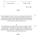
- FIG. 4 is a schematic flowchart of a method for controlling a storage unit 100 according to an embodiment of the present invention.
- the method is applied to the storage unit 100 provided in the foregoing embodiment, and reference may also be made to the schematic structural diagram of the storage unit 100 shown in FIG. 1 or FIG. 2 .
- the method includes the following steps:
- the storage unit 100 includes: a comb-shaped magnetic track 110, the first drive circuit 20, the second drive circuit 30, the first drive port 40 connected to the first drive circuit 20, and the second drive port 50 connected to the second drive circuit 30, where the comb-shaped magnetic track 110 includes the first storage area 111, the second storage area 112, and a comb handle 113 connected to the first storage area 111 and the second storage area 112; the first storage area 111 is disposed between the first port A and the comb handle 113, the second storage area 112 is disposed between the second port B and the comb handle 113, and at least one storage area of the first storage area 111 and the second storage area 112 includes at least two memory bars.
- the first port A on the top of the comb-shaped magnetic track 110 consists of a top port of at least two memory bars included in the first storage area 111
- the second port B on the top of the comb-shaped magnetic track 110 consists of a top port of at least two memory bars included in the second storage area 112.
- the first drive circuit 20 in the storage unit 100 includes a first gate port 201
- the second drive circuit 30 includes a second gate port 301.
- the control method further includes: switching on or off the first drive circuit 20 and switching respectively off or on the second drive circuit 30 according to values of input voltages of the first gate port 201 and the second gate port 301 that are of the storage unit 100.
- a voltage difference between two ends (that is, the first drive port 40, and a top port that corresponds to a memory bar) of a memory bar (for example, a memory bar a) in the first storage area 111 is greater than or equal to a voltage threshold for driving a magnetic domain to move, a voltage difference between two ends (that is, the first drive port 40, and a top port that corresponds to a memory bar) of another memory bar in the first storage area 111 is less than the voltage threshold for driving a magnetic domain wall to move, and a voltage difference between two ends (that is, the second drive port 50, and a top port that corresponds to a memory bar) of all memory bars in the second storage area 112 is less than the voltage threshold for driving a magnetic domain wall to move, and in addition, a value of a voltage of
- a voltage of each port of the storage unit 100 is controlled, so that a memory bar in the first storage area 111 and a memory bar in the second storage area 112 do not work at the same time, that is, a read operation or a write operation is controlled to be performed on only one memory bar each time.
- the storage unit 100 further includes a write circuit 60 and a read circuit 70 that are disposed at the bottom of the comb-shaped magnetic track 110, and a storage module connected to the read circuit 70. Therefore, the method further includes: performing, by the write circuit 60, a write operation on the first storage area 111 and the second storage area 112, and performing, by the read circuit 70, a read operation on the first storage area 111 and the second storage area 112; and when a magnetic domain in a memory bar (for example, a) in the first storage area 111 or in a memory bar (for example, b) in the second storage area 112 moves, storing, by the storage module, data that read out from the comb-shaped magnetic track 110.
- a memory bar for example, a
- the method for controlling a storage unit 100 according to this embodiment of the present invention is applied to the storage unit 100 described in the foregoing embodiment, and in the method, more than two memory bars in the storage unit 100 are controlled and may all be used for storing data, which increases storage density; in addition, compared with a method for controlling two memory bars by using one pair of read and write apparatuses, a method for controlling more than two memory bars by using only one pair of read and write apparatuses reduces manufacturing costs; in addition, in the method, a current pulse provided by a drive circuit in the storage unit 100 is further controlled and needs to drive only a magnetic domain wall in a memory bar on one side of a track to move, and therefore, a drive voltage can be reduced and power consumption can also be reduced.
- unit division is merely logical function division and may be other division in actual implementation.
- control units in the embodiments of the present invention may be integrated into one processing unit, or each of the units may exist alone physically, or two or more units are integrated into one unit.
- the integrated unit may be implemented in a form of hardware, or may be implemented in a form of a software control unit.
- the integrated unit When the integrated unit is implemented in the form of a software control unit and sold or used as an independent product, the integrated unit may be stored in a computer-readable storage medium. Based on such an understanding, the control unit may be implemented in the form of a software product.
- the software product is stored in a storage medium and includes several instructions for instructing a computer device (which may be a personal computer, a server, or a network device) to perform all or some of the steps of the methods described in the embodiments of the present invention.
- the foregoing storage medium includes: any medium that can store program code, such as a USB flash drive, a removable hard disk, a read-only memory (ROM, Read-Only Memory), a random access memory (RAM, Random Access Memory), a magnetic disk, or an optical disc.
Landscapes
- Engineering & Computer Science (AREA)
- Computer Hardware Design (AREA)
- Mram Or Spin Memory Techniques (AREA)
- Hall/Mr Elements (AREA)
Claims (6)
- Speichereinheit, die Folgendes umfasst:
eine kammartige Magnetspur (110), eine erste Ansteuerschaltung (20), eine zweite Ansteuerschaltung (30), einen ersten Ansteueranschluss (40), der mit der ersten Ansteuerschaltung (20) verbunden ist, und einen zweiten Ansteueranschluss (50), der mit der zweiten Ansteuerschaltung (30) verbunden ist, wobei:die kammartige Magnetspur (110) einen ersten Speicherbereich (111), einen zweiten Speicherbereich (112) und einen Kammbügel (113), der mit dem ersten Speicherbereich (111) und dem zweiten Speicherbereich (112) verbunden ist, umfasst und wenigstens ein Speicherbereich aus dem ersten Speicherbereich (111) und dem zweiten Speicherbereich (112) wenigstens zwei Datenspeicherriegel umfasst;wobei die erste Ansteuerschaltung (20) zwischen dem ersten Ansteueranschluss (40) und dem ersten Speicherbereich (111) verbunden ist und der erste Speicherbereich (111) zwischen einem ersten Anschluss (A) und der ersten Ansteuerschaltung (20) verbunden ist; undwobei die zweite Ansteuerschaltung (30) zwischen dem zweiten Ansteueranschluss (50) und dem zweiten Speicherbereich (112) verbunden ist und der zweite Speicherbereich (111) zwischen einem zweiten Anschluss (B) und der zweiten Ansteuerschaltung (30) verbunden ist;Steuermittel, die konfiguriert sind, eine erste Gruppe von Eingangsspannungen an den ersten Anschluss (A), den zweiten Anschluss (B), den ersten Ansteueranschluss (40) und den zweiten Ansteueranschluss (50) anzulegen und die erste Ansteuerschaltung (20) so anzusteuern, dass ein Stromimpuls in einem Datenspeicherriegel in dem ersten Speicherbereich (111) erzeugt wird, und eine magnetische Domänenwand in dem Datenspeicherriegel, in dem der Stromimpuls erzeugt wird, angesteuert wird, sich zu verlagern; undwobei die Steuermittel außerdem konfiguriert sind, eine zweite Gruppe von Eingangsspannungen an den ersten Anschluss (A), den zweiten Anschluss (B), den ersten Ansteueranschluss (40) und den zweiten Ansteueranschluss (50) anzulegen unddie zweite Ansteuerschaltung (30) so anzusteuern, dass ein Stromimpuls in einem Datenspeicherriegel in dem zweiten Speicherbereich (112) erzeugt wird, und eine magnetische Domänenwand in dem Datenspeicherriegel, in dem der Stromimpuls erzeugt wird, angesteuert wird, sich zu verlagern,dadurch gekennzeichnet, dassdie erste Ansteuerschaltung (20) einen ersten "Gate"-Anschluss (201) umfasst und die zweite Ansteuerschaltung (30) einen zweiten "Gate"-Anschluss (301) umfasst, wobei der erste "Gate"-Anschluss (201) konfiguriert ist, das An- oder Abschalten der ersten Ansteuerschaltung (20) gemäß einem Wert einer an den ersten "Gate"-Anschluss (201) angelegten Spannung zu steuern, und der zweite "Gate"-Anschluss (301) konfiguriert ist, das An- und Abschalten der zweiten Ansteuerschaltung (30) gemäß einem Wert einer an den zweiten "Gate"-Anschluss (301) angelegten Spannung zu steuern, wobei die Steuermittel so konfiguriert sind, dass dann, wenn die erste Gruppe von Eingangsspannungen durch die Steuermittel angelegt ist, der Wert der Spannung, die an den ersten "Gate"-Anschluss angelegt ist, die erste Ansteuerschaltung anschaltet,und der Wert der Spannung, die an den zweiten "Gate"-Anschluss angelegt ist, die zweite Ansteuerschaltung abschaltet, und so, dass dann, wenn die zweite Gruppe von Eingangsspannungen durch die Steuermittel angelegt ist, der Wert der Spannung, die an den ersten "Gate"-Anschluss angelegt ist, die erste Ansteuerschaltung abschaltet,und der Wert der Spannung, die an den zweiten "Gate"-Anschluss angelegt ist, die zweite Ansteuerschaltung anschaltet; undwobei die Speichereinheit ferner eine Schreibschaltung (60) und eine Leseschaltung (70) umfasst, die an der Unterseite der kammartigen Magnetspur (110) angeordnet sind, wobei die Schreibschaltung (60) konfiguriert ist, eine Schreiboperation auf einem Datenspeicherriegel in dem ersten Speicherbereich (111) und einem Datenspeicherriegel in dem zweiten Speicherbereich (122) auszuführen und sich die Schreibschaltung (60) auf einer ersten Seite des Kammbügels befindet und mit einer Domäne der Magnetspur in dem Kammbügel magnetisch gekoppelt ist, wobei der erste (111) und der zweite (112) Speicherbereich auf einer zweiten Seite des Kammbügels sind und die zweite Seite der ersten Seite entgegengesetzt ist. - Speichereinheit nach Anspruch 1, wobei:
der erste Speicherbereich (111) zwischen dem ersten Anschluss (A) und dem Kammbügel (113) angeordnet ist, und der zweite Speicherbereich (112) zwischen dem zweiten Anschluss (B) und dem Kammbügel (113) angeordnet ist. - Speichereinheit nach Anspruch 1 oder 2, wobei:
die Speichereinheit ferner ein Speichermodul, das mit der Leseschaltung (70) verbunden ist, umfasst, wobei das Speichermodul konfiguriert ist: wenn sich eine magnetische Domänenwand in einem Datenspeicherriegel in der kammartigen Magnetspur verlagert, Daten, die aus der kammartigen Magnetspur (110) gelesen werden, zu speichern. - Datenspeicher, der wenigstens eine der Speichereinheit nach einem der Ansprüche 1 bis 3 umfasst.
- Verfahren zum Steuern der Speichereinheit nach Anspruch 1, wobei das Verfahren Folgendes umfasst:durch Steuern der Eingangsspannungen des ersten Anschlusses (A), des zweiten Anschlusses (B), des ersten Ansteueranschlusses (40) und des zweiten Ansteueranschlusses (50), die zu der Speichereinheit gehören, und Ansteuern der ersten Ansteuerschaltung (29) Erzeugen eines Stromimpulses in dem Datenspeicherriegel in dem ersten Speicherbereich (111) der Speichereinheit, undAnsteuern einer magnetischen Domänenwand in dem Datenspeicherriegel, in dem der Stromimpuls erzeugt wird, sich zu verlagern; unddurch Steuern der Eingangsspannungen des ersten Anschlusses (A), des zweiten Anschlusses (B), des ersten Ansteueranschlusses (40) und des zweiten Ansteueranschlusses (50) und Ansteuern der zweiten Ansteuerschaltung (30) Erzeugen eines Stromimpulses in dem Datenspeicherriegel in dem zweiten Speicherbereich (112) der Speichereinheit, und Ansteuern einer magnetischen Domänenwand in dem Datenspeicherriegel, in dem der Stromimpuls erzeugt wird, sich zu verlagern.
- Steuerverfahren nach Anspruch 5, wobei das Verfahren ferner Folgendes umfasst:
Verbinden des ersten Ansteueranschlusses (40) oder Verbinden des zweiten Ansteueranschlusses (50) mit dem Kammbügel (113) gemäß den Werten der an den ersten "Gate"-Anschluss (201) und den zweiten "Gate"-Anschluss (301) angelegten Spannungen.
Applications Claiming Priority (2)
| Application Number | Priority Date | Filing Date | Title |
|---|---|---|---|
| CN201310496705.2A CN104575582B (zh) | 2013-10-21 | 2013-10-21 | 一种存储单元、存储器及存储单元控制方法 |
| PCT/CN2014/089044 WO2015058674A1 (zh) | 2013-10-21 | 2014-10-21 | 一种存储单元、存储器及存储单元控制方法 |
Publications (3)
| Publication Number | Publication Date |
|---|---|
| EP3048611A1 EP3048611A1 (de) | 2016-07-27 |
| EP3048611A4 EP3048611A4 (de) | 2016-10-19 |
| EP3048611B1 true EP3048611B1 (de) | 2022-04-06 |
Family
ID=52992274
Family Applications (1)
| Application Number | Title | Priority Date | Filing Date |
|---|---|---|---|
| EP14856459.4A Active EP3048611B1 (de) | 2013-10-21 | 2014-10-21 | Speichereinheit, speicher und steuerungsverfahren für die speichereinheit |
Country Status (5)
| Country | Link |
|---|---|
| US (1) | US9653178B2 (de) |
| EP (1) | EP3048611B1 (de) |
| KR (1) | KR101814029B1 (de) |
| CN (1) | CN104575582B (de) |
| WO (1) | WO2015058674A1 (de) |
Families Citing this family (3)
| Publication number | Priority date | Publication date | Assignee | Title |
|---|---|---|---|---|
| CN104575581B (zh) | 2013-10-21 | 2017-10-10 | 华为技术有限公司 | 一种存储单元、存储器及存储单元控制方法 |
| KR102798078B1 (ko) | 2019-08-16 | 2025-04-22 | 삼성전자주식회사 | 자기 메모리 장치 |
| CN117174139B (zh) * | 2023-08-25 | 2024-06-18 | 合芯科技(苏州)有限公司 | 一种信号生成电路及存储器 |
Family Cites Families (9)
| Publication number | Priority date | Publication date | Assignee | Title |
|---|---|---|---|---|
| KR100790886B1 (ko) * | 2006-09-15 | 2008-01-03 | 삼성전자주식회사 | 자구 벽 이동을 이용한 정보 저장 장치 |
| KR100813270B1 (ko) | 2006-09-29 | 2008-03-13 | 삼성전자주식회사 | 자구벽 이동을 이용한 데이터 저장 장치 및 그의 동작 방법 |
| KR100868761B1 (ko) * | 2006-11-20 | 2008-11-13 | 삼성전자주식회사 | 자구벽 이동을 이용한 정보 저장 매체 |
| US7952906B2 (en) | 2006-12-22 | 2011-05-31 | Samsung Electronics Co., Ltd. | Information storage devices using magnetic domain wall movement and methods of manufacturing the same |
| KR101323719B1 (ko) * | 2007-10-12 | 2013-10-30 | 삼성전자주식회사 | 자성층, 자성층의 형성방법, 자성층을 포함하는정보저장장치 및 정보저장장치의 제조방법 |
| KR101466237B1 (ko) * | 2008-07-14 | 2014-12-01 | 삼성전자주식회사 | 자구벽 이동을 이용한 정보저장장치 및 그 동작방법 |
| US7626844B1 (en) | 2008-08-22 | 2009-12-01 | International Business Machines Corporation | Magnetic racetrack with current-controlled motion of domain walls within an undulating energy landscape |
| US7551469B1 (en) | 2009-01-05 | 2009-06-23 | Internationa Business Machines Corporation | Unidirectional racetrack memory device |
| KR20100104044A (ko) | 2009-03-16 | 2010-09-29 | 삼성전자주식회사 | 정보저장장치 및 그의 동작방법 |
-
2013
- 2013-10-21 CN CN201310496705.2A patent/CN104575582B/zh active Active
-
2014
- 2014-10-21 WO PCT/CN2014/089044 patent/WO2015058674A1/zh not_active Ceased
- 2014-10-21 EP EP14856459.4A patent/EP3048611B1/de active Active
- 2014-10-21 KR KR1020167012523A patent/KR101814029B1/ko active Active
-
2016
- 2016-04-20 US US15/133,452 patent/US9653178B2/en active Active
Also Published As
| Publication number | Publication date |
|---|---|
| EP3048611A4 (de) | 2016-10-19 |
| EP3048611A1 (de) | 2016-07-27 |
| US20160232984A1 (en) | 2016-08-11 |
| WO2015058674A1 (zh) | 2015-04-30 |
| CN104575582A (zh) | 2015-04-29 |
| KR101814029B1 (ko) | 2018-01-02 |
| US9653178B2 (en) | 2017-05-16 |
| KR20160069518A (ko) | 2016-06-16 |
| CN104575582B (zh) | 2018-05-04 |
Similar Documents
| Publication | Publication Date | Title |
|---|---|---|
| EP3828889A1 (de) | Speicherschaltung | |
| CN101939838B (zh) | 多个存储器单元和方法 | |
| US20100002486A1 (en) | Magnetic shift register memory device | |
| EP3051536B1 (de) | Speichereinheit, speicher und speichereinheitsteuerungsverfahren | |
| TWI753608B (zh) | 具極性轉變能力之多工解碼器 | |
| US9653178B2 (en) | Magnetic track storage unit, memory, and method for controlling magnetic track storage unit | |
| CN115249493A (zh) | 记忆体阵列、其系统及其操作方法 | |
| US11847944B2 (en) | Data distribution for holographic projection | |
| SG185894A1 (en) | A current writing circuit for a resistive memory cell arrangement | |
| JP5212378B2 (ja) | 半導体装置のコンフィギュレーション方法 | |
| CN103377691A (zh) | 具有字级功率门控的存储器 | |
| US11527286B2 (en) | Voltage drivers with reduced power consumption during polarity transition | |
| TWI891732B (zh) | 記憶體陣列及系統 | |
| US20250069634A1 (en) | Ferroelectric memory, control apparatus thereof, method for increasing endurance of ferroelectric memory, and device | |
| CN104425023B (zh) | 具有公共源极线屏蔽电路的存储器设备 | |
| WO2016066053A1 (zh) | 一种磁性存储器 | |
| US11127436B2 (en) | Memory array with access line control having a shunt sense line | |
| KR20220064405A (ko) | 집적 회로 메모리에서의 읽기 스파이크 완화 | |
| CN105469820A (zh) | 一种磁性存储装置、磁性存储阵列结构及其驱动方法 | |
| CN113544780A (zh) | 半导体电路和电子设备 |
Legal Events
| Date | Code | Title | Description |
|---|---|---|---|
| PUAI | Public reference made under article 153(3) epc to a published international application that has entered the european phase |
Free format text: ORIGINAL CODE: 0009012 |
|
| 17P | Request for examination filed |
Effective date: 20160422 |
|
| AK | Designated contracting states |
Kind code of ref document: A1 Designated state(s): AL AT BE BG CH CY CZ DE DK EE ES FI FR GB GR HR HU IE IS IT LI LT LU LV MC MK MT NL NO PL PT RO RS SE SI SK SM TR |
|
| AX | Request for extension of the european patent |
Extension state: BA ME |
|
| RIN1 | Information on inventor provided before grant (corrected) |
Inventor name: LIN, YINYIN Inventor name: FU, YARONG Inventor name: ZHAO, JUNFENG Inventor name: YANG, WEI Inventor name: WEI, ZHULIN Inventor name: YANG, KAI |
|
| A4 | Supplementary search report drawn up and despatched |
Effective date: 20160921 |
|
| RIC1 | Information provided on ipc code assigned before grant |
Ipc: G11C 11/02 20060101AFI20160915BHEP Ipc: G11C 11/15 20060101ALI20160915BHEP Ipc: G11C 19/08 20060101ALI20160915BHEP |
|
| DAX | Request for extension of the european patent (deleted) | ||
| STAA | Information on the status of an ep patent application or granted ep patent |
Free format text: STATUS: EXAMINATION IS IN PROGRESS |
|
| 17Q | First examination report despatched |
Effective date: 20180926 |
|
| REG | Reference to a national code |
Ref country code: DE Ref legal event code: R079 Ref document number: 602014083161 Country of ref document: DE Free format text: PREVIOUS MAIN CLASS: G11C0011020000 Ipc: G11C0011150000 |
|
| GRAP | Despatch of communication of intention to grant a patent |
Free format text: ORIGINAL CODE: EPIDOSNIGR1 |
|
| STAA | Information on the status of an ep patent application or granted ep patent |
Free format text: STATUS: GRANT OF PATENT IS INTENDED |
|
| GRAJ | Information related to disapproval of communication of intention to grant by the applicant or resumption of examination proceedings by the epo deleted |
Free format text: ORIGINAL CODE: EPIDOSDIGR1 |
|
| GRAP | Despatch of communication of intention to grant a patent |
Free format text: ORIGINAL CODE: EPIDOSNIGR1 |
|
| RIC1 | Information provided on ipc code assigned before grant |
Ipc: G11C 19/08 20060101ALI20210928BHEP Ipc: G11C 11/16 20060101ALI20210928BHEP Ipc: G11C 11/15 20060101AFI20210928BHEP |
|
| INTG | Intention to grant announced |
Effective date: 20211012 |
|
| INTG | Intention to grant announced |
Effective date: 20211027 |
|
| GRAS | Grant fee paid |
Free format text: ORIGINAL CODE: EPIDOSNIGR3 |
|
| GRAA | (expected) grant |
Free format text: ORIGINAL CODE: 0009210 |
|
| STAA | Information on the status of an ep patent application or granted ep patent |
Free format text: STATUS: THE PATENT HAS BEEN GRANTED |
|
| AK | Designated contracting states |
Kind code of ref document: B1 Designated state(s): AL AT BE BG CH CY CZ DE DK EE ES FI FR GB GR HR HU IE IS IT LI LT LU LV MC MK MT NL NO PL PT RO RS SE SI SK SM TR |
|
| REG | Reference to a national code |
Ref country code: GB Ref legal event code: FG4D |
|
| REG | Reference to a national code |
Ref country code: CH Ref legal event code: EP |
|
| REG | Reference to a national code |
Ref country code: AT Ref legal event code: REF Ref document number: 1482162 Country of ref document: AT Kind code of ref document: T Effective date: 20220415 |
|
| REG | Reference to a national code |
Ref country code: IE Ref legal event code: FG4D |
|
| REG | Reference to a national code |
Ref country code: DE Ref legal event code: R096 Ref document number: 602014083161 Country of ref document: DE |
|
| REG | Reference to a national code |
Ref country code: LT Ref legal event code: MG9D |
|
| REG | Reference to a national code |
Ref country code: NL Ref legal event code: MP Effective date: 20220406 |
|
| REG | Reference to a national code |
Ref country code: AT Ref legal event code: MK05 Ref document number: 1482162 Country of ref document: AT Kind code of ref document: T Effective date: 20220406 |
|
| PG25 | Lapsed in a contracting state [announced via postgrant information from national office to epo] |
Ref country code: NL Free format text: LAPSE BECAUSE OF FAILURE TO SUBMIT A TRANSLATION OF THE DESCRIPTION OR TO PAY THE FEE WITHIN THE PRESCRIBED TIME-LIMIT Effective date: 20220406 |
|
| PG25 | Lapsed in a contracting state [announced via postgrant information from national office to epo] |
Ref country code: SE Free format text: LAPSE BECAUSE OF FAILURE TO SUBMIT A TRANSLATION OF THE DESCRIPTION OR TO PAY THE FEE WITHIN THE PRESCRIBED TIME-LIMIT Effective date: 20220406 Ref country code: PT Free format text: LAPSE BECAUSE OF FAILURE TO SUBMIT A TRANSLATION OF THE DESCRIPTION OR TO PAY THE FEE WITHIN THE PRESCRIBED TIME-LIMIT Effective date: 20220808 Ref country code: NO Free format text: LAPSE BECAUSE OF FAILURE TO SUBMIT A TRANSLATION OF THE DESCRIPTION OR TO PAY THE FEE WITHIN THE PRESCRIBED TIME-LIMIT Effective date: 20220706 Ref country code: LT Free format text: LAPSE BECAUSE OF FAILURE TO SUBMIT A TRANSLATION OF THE DESCRIPTION OR TO PAY THE FEE WITHIN THE PRESCRIBED TIME-LIMIT Effective date: 20220406 Ref country code: HR Free format text: LAPSE BECAUSE OF FAILURE TO SUBMIT A TRANSLATION OF THE DESCRIPTION OR TO PAY THE FEE WITHIN THE PRESCRIBED TIME-LIMIT Effective date: 20220406 Ref country code: GR Free format text: LAPSE BECAUSE OF FAILURE TO SUBMIT A TRANSLATION OF THE DESCRIPTION OR TO PAY THE FEE WITHIN THE PRESCRIBED TIME-LIMIT Effective date: 20220707 Ref country code: FI Free format text: LAPSE BECAUSE OF FAILURE TO SUBMIT A TRANSLATION OF THE DESCRIPTION OR TO PAY THE FEE WITHIN THE PRESCRIBED TIME-LIMIT Effective date: 20220406 Ref country code: ES Free format text: LAPSE BECAUSE OF FAILURE TO SUBMIT A TRANSLATION OF THE DESCRIPTION OR TO PAY THE FEE WITHIN THE PRESCRIBED TIME-LIMIT Effective date: 20220406 Ref country code: BG Free format text: LAPSE BECAUSE OF FAILURE TO SUBMIT A TRANSLATION OF THE DESCRIPTION OR TO PAY THE FEE WITHIN THE PRESCRIBED TIME-LIMIT Effective date: 20220706 Ref country code: AT Free format text: LAPSE BECAUSE OF FAILURE TO SUBMIT A TRANSLATION OF THE DESCRIPTION OR TO PAY THE FEE WITHIN THE PRESCRIBED TIME-LIMIT Effective date: 20220406 |
|
| PG25 | Lapsed in a contracting state [announced via postgrant information from national office to epo] |
Ref country code: RS Free format text: LAPSE BECAUSE OF FAILURE TO SUBMIT A TRANSLATION OF THE DESCRIPTION OR TO PAY THE FEE WITHIN THE PRESCRIBED TIME-LIMIT Effective date: 20220406 Ref country code: PL Free format text: LAPSE BECAUSE OF FAILURE TO SUBMIT A TRANSLATION OF THE DESCRIPTION OR TO PAY THE FEE WITHIN THE PRESCRIBED TIME-LIMIT Effective date: 20220406 Ref country code: LV Free format text: LAPSE BECAUSE OF FAILURE TO SUBMIT A TRANSLATION OF THE DESCRIPTION OR TO PAY THE FEE WITHIN THE PRESCRIBED TIME-LIMIT Effective date: 20220406 Ref country code: IS Free format text: LAPSE BECAUSE OF FAILURE TO SUBMIT A TRANSLATION OF THE DESCRIPTION OR TO PAY THE FEE WITHIN THE PRESCRIBED TIME-LIMIT Effective date: 20220806 |
|
| REG | Reference to a national code |
Ref country code: DE Ref legal event code: R097 Ref document number: 602014083161 Country of ref document: DE |
|
| PG25 | Lapsed in a contracting state [announced via postgrant information from national office to epo] |
Ref country code: SM Free format text: LAPSE BECAUSE OF FAILURE TO SUBMIT A TRANSLATION OF THE DESCRIPTION OR TO PAY THE FEE WITHIN THE PRESCRIBED TIME-LIMIT Effective date: 20220406 Ref country code: SK Free format text: LAPSE BECAUSE OF FAILURE TO SUBMIT A TRANSLATION OF THE DESCRIPTION OR TO PAY THE FEE WITHIN THE PRESCRIBED TIME-LIMIT Effective date: 20220406 Ref country code: RO Free format text: LAPSE BECAUSE OF FAILURE TO SUBMIT A TRANSLATION OF THE DESCRIPTION OR TO PAY THE FEE WITHIN THE PRESCRIBED TIME-LIMIT Effective date: 20220406 Ref country code: EE Free format text: LAPSE BECAUSE OF FAILURE TO SUBMIT A TRANSLATION OF THE DESCRIPTION OR TO PAY THE FEE WITHIN THE PRESCRIBED TIME-LIMIT Effective date: 20220406 Ref country code: DK Free format text: LAPSE BECAUSE OF FAILURE TO SUBMIT A TRANSLATION OF THE DESCRIPTION OR TO PAY THE FEE WITHIN THE PRESCRIBED TIME-LIMIT Effective date: 20220406 Ref country code: CZ Free format text: LAPSE BECAUSE OF FAILURE TO SUBMIT A TRANSLATION OF THE DESCRIPTION OR TO PAY THE FEE WITHIN THE PRESCRIBED TIME-LIMIT Effective date: 20220406 |
|
| PLBE | No opposition filed within time limit |
Free format text: ORIGINAL CODE: 0009261 |
|
| STAA | Information on the status of an ep patent application or granted ep patent |
Free format text: STATUS: NO OPPOSITION FILED WITHIN TIME LIMIT |
|
| 26N | No opposition filed |
Effective date: 20230110 |
|
| PG25 | Lapsed in a contracting state [announced via postgrant information from national office to epo] |
Ref country code: AL Free format text: LAPSE BECAUSE OF FAILURE TO SUBMIT A TRANSLATION OF THE DESCRIPTION OR TO PAY THE FEE WITHIN THE PRESCRIBED TIME-LIMIT Effective date: 20220406 |
|
| PG25 | Lapsed in a contracting state [announced via postgrant information from national office to epo] |
Ref country code: SI Free format text: LAPSE BECAUSE OF FAILURE TO SUBMIT A TRANSLATION OF THE DESCRIPTION OR TO PAY THE FEE WITHIN THE PRESCRIBED TIME-LIMIT Effective date: 20220406 Ref country code: MC Free format text: LAPSE BECAUSE OF FAILURE TO SUBMIT A TRANSLATION OF THE DESCRIPTION OR TO PAY THE FEE WITHIN THE PRESCRIBED TIME-LIMIT Effective date: 20220406 |
|
| REG | Reference to a national code |
Ref country code: CH Ref legal event code: PL |
|
| REG | Reference to a national code |
Ref country code: BE Ref legal event code: MM Effective date: 20221031 |
|
| GBPC | Gb: european patent ceased through non-payment of renewal fee |
Effective date: 20221021 |
|
| PG25 | Lapsed in a contracting state [announced via postgrant information from national office to epo] |
Ref country code: LU Free format text: LAPSE BECAUSE OF NON-PAYMENT OF DUE FEES Effective date: 20221021 |
|
| PG25 | Lapsed in a contracting state [announced via postgrant information from national office to epo] |
Ref country code: LI Free format text: LAPSE BECAUSE OF NON-PAYMENT OF DUE FEES Effective date: 20221031 Ref country code: FR Free format text: LAPSE BECAUSE OF NON-PAYMENT OF DUE FEES Effective date: 20221031 Ref country code: CH Free format text: LAPSE BECAUSE OF NON-PAYMENT OF DUE FEES Effective date: 20221031 |
|
| PG25 | Lapsed in a contracting state [announced via postgrant information from national office to epo] |
Ref country code: BE Free format text: LAPSE BECAUSE OF NON-PAYMENT OF DUE FEES Effective date: 20221031 |
|
| PG25 | Lapsed in a contracting state [announced via postgrant information from national office to epo] |
Ref country code: IE Free format text: LAPSE BECAUSE OF NON-PAYMENT OF DUE FEES Effective date: 20221021 Ref country code: GB Free format text: LAPSE BECAUSE OF NON-PAYMENT OF DUE FEES Effective date: 20221021 |
|
| PG25 | Lapsed in a contracting state [announced via postgrant information from national office to epo] |
Ref country code: IT Free format text: LAPSE BECAUSE OF FAILURE TO SUBMIT A TRANSLATION OF THE DESCRIPTION OR TO PAY THE FEE WITHIN THE PRESCRIBED TIME-LIMIT Effective date: 20220406 |
|
| PG25 | Lapsed in a contracting state [announced via postgrant information from national office to epo] |
Ref country code: HU Free format text: LAPSE BECAUSE OF FAILURE TO SUBMIT A TRANSLATION OF THE DESCRIPTION OR TO PAY THE FEE WITHIN THE PRESCRIBED TIME-LIMIT; INVALID AB INITIO Effective date: 20141021 |
|
| PG25 | Lapsed in a contracting state [announced via postgrant information from national office to epo] |
Ref country code: CY Free format text: LAPSE BECAUSE OF FAILURE TO SUBMIT A TRANSLATION OF THE DESCRIPTION OR TO PAY THE FEE WITHIN THE PRESCRIBED TIME-LIMIT Effective date: 20220406 |
|
| PG25 | Lapsed in a contracting state [announced via postgrant information from national office to epo] |
Ref country code: MK Free format text: LAPSE BECAUSE OF FAILURE TO SUBMIT A TRANSLATION OF THE DESCRIPTION OR TO PAY THE FEE WITHIN THE PRESCRIBED TIME-LIMIT Effective date: 20220406 |
|
| PG25 | Lapsed in a contracting state [announced via postgrant information from national office to epo] |
Ref country code: TR Free format text: LAPSE BECAUSE OF FAILURE TO SUBMIT A TRANSLATION OF THE DESCRIPTION OR TO PAY THE FEE WITHIN THE PRESCRIBED TIME-LIMIT Effective date: 20220406 |
|
| PG25 | Lapsed in a contracting state [announced via postgrant information from national office to epo] |
Ref country code: MT Free format text: LAPSE BECAUSE OF FAILURE TO SUBMIT A TRANSLATION OF THE DESCRIPTION OR TO PAY THE FEE WITHIN THE PRESCRIBED TIME-LIMIT Effective date: 20220406 |
|
| PG25 | Lapsed in a contracting state [announced via postgrant information from national office to epo] |
Ref country code: BG Free format text: LAPSE BECAUSE OF FAILURE TO SUBMIT A TRANSLATION OF THE DESCRIPTION OR TO PAY THE FEE WITHIN THE PRESCRIBED TIME-LIMIT Effective date: 20220406 |
|
| PG25 | Lapsed in a contracting state [announced via postgrant information from national office to epo] |
Ref country code: BG Free format text: LAPSE BECAUSE OF FAILURE TO SUBMIT A TRANSLATION OF THE DESCRIPTION OR TO PAY THE FEE WITHIN THE PRESCRIBED TIME-LIMIT Effective date: 20220406 |
|
| PGFP | Annual fee paid to national office [announced via postgrant information from national office to epo] |
Ref country code: DE Payment date: 20250902 Year of fee payment: 12 |