EP3044654B1 - Capacitive sensor for detecting touch position and pressing force - Google Patents
Capacitive sensor for detecting touch position and pressing force Download PDFInfo
- Publication number
- EP3044654B1 EP3044654B1 EP14759066.5A EP14759066A EP3044654B1 EP 3044654 B1 EP3044654 B1 EP 3044654B1 EP 14759066 A EP14759066 A EP 14759066A EP 3044654 B1 EP3044654 B1 EP 3044654B1
- Authority
- EP
- European Patent Office
- Prior art keywords
- electrode
- substrate
- wires
- electrode wires
- structures
- Prior art date
- Legal status (The legal status is an assumption and is not a legal conclusion. Google has not performed a legal analysis and makes no representation as to the accuracy of the status listed.)
- Not-in-force
Links
- 238000003825 pressing Methods 0.000 title claims description 22
- 239000000758 substrate Substances 0.000 claims description 162
- 239000004020 conductor Substances 0.000 claims description 66
- 229910052751 metal Inorganic materials 0.000 claims description 40
- 239000002184 metal Substances 0.000 claims description 40
- 230000009975 flexible effect Effects 0.000 claims description 36
- 230000008859 change Effects 0.000 claims description 29
- 239000000463 material Substances 0.000 claims description 13
- 238000005452 bending Methods 0.000 claims description 2
- 239000010410 layer Substances 0.000 description 75
- 238000001514 detection method Methods 0.000 description 67
- 238000004364 calculation method Methods 0.000 description 13
- 239000012790 adhesive layer Substances 0.000 description 10
- 230000008878 coupling Effects 0.000 description 9
- 238000010168 coupling process Methods 0.000 description 9
- 238000005859 coupling reaction Methods 0.000 description 9
- 230000006870 function Effects 0.000 description 7
- 230000001070 adhesive effect Effects 0.000 description 6
- 239000011347 resin Substances 0.000 description 6
- 229920005989 resin Polymers 0.000 description 6
- 239000000853 adhesive Substances 0.000 description 5
- 230000000694 effects Effects 0.000 description 5
- 238000005304 joining Methods 0.000 description 5
- 238000000034 method Methods 0.000 description 5
- -1 poly(ethylene terephthalate) Polymers 0.000 description 5
- 230000002265 prevention Effects 0.000 description 5
- 230000035945 sensitivity Effects 0.000 description 5
- 239000011888 foil Substances 0.000 description 4
- 229920000139 polyethylene terephthalate Polymers 0.000 description 4
- 239000005020 polyethylene terephthalate Substances 0.000 description 4
- 238000000151 deposition Methods 0.000 description 3
- 230000008021 deposition Effects 0.000 description 3
- 238000010586 diagram Methods 0.000 description 3
- 238000005401 electroluminescence Methods 0.000 description 3
- 239000002985 plastic film Substances 0.000 description 3
- 125000006850 spacer group Chemical group 0.000 description 3
- 239000004820 Pressure-sensitive adhesive Substances 0.000 description 2
- 239000003990 capacitor Substances 0.000 description 2
- 230000000052 comparative effect Effects 0.000 description 2
- 239000010949 copper Substances 0.000 description 2
- 238000006073 displacement reaction Methods 0.000 description 2
- 239000013013 elastic material Substances 0.000 description 2
- WABPQHHGFIMREM-UHFFFAOYSA-N lead(0) Chemical compound [Pb] WABPQHHGFIMREM-UHFFFAOYSA-N 0.000 description 2
- 239000011777 magnesium Substances 0.000 description 2
- 239000011159 matrix material Substances 0.000 description 2
- 238000007747 plating Methods 0.000 description 2
- 229920003229 poly(methyl methacrylate) Polymers 0.000 description 2
- 239000004417 polycarbonate Substances 0.000 description 2
- 229920000515 polycarbonate Polymers 0.000 description 2
- 239000004926 polymethyl methacrylate Substances 0.000 description 2
- 238000007639 printing Methods 0.000 description 2
- 230000009467 reduction Effects 0.000 description 2
- 238000004544 sputter deposition Methods 0.000 description 2
- 229910000838 Al alloy Inorganic materials 0.000 description 1
- RYGMFSIKBFXOCR-UHFFFAOYSA-N Copper Chemical compound [Cu] RYGMFSIKBFXOCR-UHFFFAOYSA-N 0.000 description 1
- FYYHWMGAXLPEAU-UHFFFAOYSA-N Magnesium Chemical compound [Mg] FYYHWMGAXLPEAU-UHFFFAOYSA-N 0.000 description 1
- 239000004642 Polyimide Substances 0.000 description 1
- 239000004840 adhesive resin Substances 0.000 description 1
- 229920006223 adhesive resin Polymers 0.000 description 1
- 229910045601 alloy Inorganic materials 0.000 description 1
- 239000000956 alloy Substances 0.000 description 1
- 229910052782 aluminium Inorganic materials 0.000 description 1
- XAGFODPZIPBFFR-UHFFFAOYSA-N aluminium Chemical compound [Al] XAGFODPZIPBFFR-UHFFFAOYSA-N 0.000 description 1
- 230000008901 benefit Effects 0.000 description 1
- 239000004918 carbon fiber reinforced polymer Substances 0.000 description 1
- 239000011248 coating agent Substances 0.000 description 1
- 239000011247 coating layer Substances 0.000 description 1
- 238000000576 coating method Methods 0.000 description 1
- 229910052802 copper Inorganic materials 0.000 description 1
- 238000009826 distribution Methods 0.000 description 1
- 230000005489 elastic deformation Effects 0.000 description 1
- 238000005516 engineering process Methods 0.000 description 1
- 230000005484 gravity Effects 0.000 description 1
- 238000007641 inkjet printing Methods 0.000 description 1
- 239000011810 insulating material Substances 0.000 description 1
- 239000011229 interlayer Substances 0.000 description 1
- 239000004973 liquid crystal related substance Substances 0.000 description 1
- 229910052749 magnesium Inorganic materials 0.000 description 1
- 238000004519 manufacturing process Methods 0.000 description 1
- 239000007769 metal material Substances 0.000 description 1
- 230000004048 modification Effects 0.000 description 1
- 238000012986 modification Methods 0.000 description 1
- 238000007645 offset printing Methods 0.000 description 1
- 238000000059 patterning Methods 0.000 description 1
- 238000000206 photolithography Methods 0.000 description 1
- 239000004033 plastic Substances 0.000 description 1
- 229920003023 plastic Polymers 0.000 description 1
- 229920001721 polyimide Polymers 0.000 description 1
- 230000008569 process Effects 0.000 description 1
- 238000004080 punching Methods 0.000 description 1
- 238000007650 screen-printing Methods 0.000 description 1
- 238000003860 storage Methods 0.000 description 1
Images


Classifications
-
- G—PHYSICS
- G06—COMPUTING; CALCULATING OR COUNTING
- G06F—ELECTRIC DIGITAL DATA PROCESSING
- G06F3/00—Input arrangements for transferring data to be processed into a form capable of being handled by the computer; Output arrangements for transferring data from processing unit to output unit, e.g. interface arrangements
- G06F3/01—Input arrangements or combined input and output arrangements for interaction between user and computer
- G06F3/03—Arrangements for converting the position or the displacement of a member into a coded form
- G06F3/041—Digitisers, e.g. for touch screens or touch pads, characterised by the transducing means
- G06F3/044—Digitisers, e.g. for touch screens or touch pads, characterised by the transducing means by capacitive means
- G06F3/0446—Digitisers, e.g. for touch screens or touch pads, characterised by the transducing means by capacitive means using a grid-like structure of electrodes in at least two directions, e.g. using row and column electrodes
-
- G—PHYSICS
- G06—COMPUTING; CALCULATING OR COUNTING
- G06F—ELECTRIC DIGITAL DATA PROCESSING
- G06F3/00—Input arrangements for transferring data to be processed into a form capable of being handled by the computer; Output arrangements for transferring data from processing unit to output unit, e.g. interface arrangements
- G06F3/01—Input arrangements or combined input and output arrangements for interaction between user and computer
- G06F3/03—Arrangements for converting the position or the displacement of a member into a coded form
- G06F3/041—Digitisers, e.g. for touch screens or touch pads, characterised by the transducing means
- G06F3/044—Digitisers, e.g. for touch screens or touch pads, characterised by the transducing means by capacitive means
- G06F3/0447—Position sensing using the local deformation of sensor cells
-
- G—PHYSICS
- G06—COMPUTING; CALCULATING OR COUNTING
- G06F—ELECTRIC DIGITAL DATA PROCESSING
- G06F3/00—Input arrangements for transferring data to be processed into a form capable of being handled by the computer; Output arrangements for transferring data from processing unit to output unit, e.g. interface arrangements
- G06F3/01—Input arrangements or combined input and output arrangements for interaction between user and computer
- G06F3/03—Arrangements for converting the position or the displacement of a member into a coded form
- G06F3/041—Digitisers, e.g. for touch screens or touch pads, characterised by the transducing means
- G06F3/0412—Digitisers structurally integrated in a display
-
- G—PHYSICS
- G06—COMPUTING; CALCULATING OR COUNTING
- G06F—ELECTRIC DIGITAL DATA PROCESSING
- G06F3/00—Input arrangements for transferring data to be processed into a form capable of being handled by the computer; Output arrangements for transferring data from processing unit to output unit, e.g. interface arrangements
- G06F3/01—Input arrangements or combined input and output arrangements for interaction between user and computer
- G06F3/03—Arrangements for converting the position or the displacement of a member into a coded form
- G06F3/041—Digitisers, e.g. for touch screens or touch pads, characterised by the transducing means
- G06F3/044—Digitisers, e.g. for touch screens or touch pads, characterised by the transducing means by capacitive means
- G06F3/0445—Digitisers, e.g. for touch screens or touch pads, characterised by the transducing means by capacitive means using two or more layers of sensing electrodes, e.g. using two layers of electrodes separated by a dielectric layer
-
- G—PHYSICS
- G06—COMPUTING; CALCULATING OR COUNTING
- G06F—ELECTRIC DIGITAL DATA PROCESSING
- G06F3/00—Input arrangements for transferring data to be processed into a form capable of being handled by the computer; Output arrangements for transferring data from processing unit to output unit, e.g. interface arrangements
- G06F3/01—Input arrangements or combined input and output arrangements for interaction between user and computer
- G06F3/03—Arrangements for converting the position or the displacement of a member into a coded form
- G06F3/041—Digitisers, e.g. for touch screens or touch pads, characterised by the transducing means
- G06F3/047—Digitisers, e.g. for touch screens or touch pads, characterised by the transducing means using sets of wires, e.g. crossed wires
-
- G—PHYSICS
- G06—COMPUTING; CALCULATING OR COUNTING
- G06F—ELECTRIC DIGITAL DATA PROCESSING
- G06F2203/00—Indexing scheme relating to G06F3/00 - G06F3/048
- G06F2203/041—Indexing scheme relating to G06F3/041 - G06F3/045
- G06F2203/04102—Flexible digitiser, i.e. constructional details for allowing the whole digitising part of a device to be flexed or rolled like a sheet of paper
-
- G—PHYSICS
- G06—COMPUTING; CALCULATING OR COUNTING
- G06F—ELECTRIC DIGITAL DATA PROCESSING
- G06F2203/00—Indexing scheme relating to G06F3/00 - G06F3/048
- G06F2203/041—Indexing scheme relating to G06F3/041 - G06F3/045
- G06F2203/04103—Manufacturing, i.e. details related to manufacturing processes specially suited for touch sensitive devices
Definitions
- the present disclosure relates to a sensor device, an input device, and an electronic apparatus that are capable of electrostatically detecting an input operation.
- a sensor device for an electronic apparatus which includes a capacitive element and is capable of detecting an operation position and a pressing force of an operation element on the input operation surface, for example, has been known (see, for example, Patent Literature 1).
- US2011/0181548A1 discloses a capacitively coupling type touch panel, including a plurality of coordinate detection electrodes for detecting X-Y position coordinates, a first substrate including the plurality of coordinate detection electrodes and a second substrate disposed to be opposed to the first substrate.
- US2001/0090175A1 discloses another capacitively coupling type touch panel, including a plurality of coordinate detection electrodes for detecting X-Y position coordinates, a first substrate including the plurality of coordinate detection electrodes and a second substrate disposed to be opposed to the first substrate.
- EP2544081A2 discloses a position detecting sensor configured by providing a dielectric member having flexibility between first conductors and second conductors and providing spacers for separating the first conductors or the second conductors from the dielectric member by a determined gap.
- US2008/0202251A1 discloses a capacitive pressure which comprises a laminated arrangement with a first flexible, electrically insulating carrier film carrying a first capacitor electrode, a second flexible, electrically insulating carrier film carrying a second capacitor electrode and a flexible, electrically insulating spacer film sandwiched between the first and second carrier films.
- US8063886B2 discloses a data input device with a film-based pressure sensor including a first carrier film, a second carrier film and a spacer.
- an input method that uses a gesture operation with a finger and has a high degree of freedom has been performed. Moreover, if a pressing force on an operation surface can be reliably detected with high accuracy, various input operations are expected to be performed. In addition, with the thickness reduction of an electronic apparatus in recent years, an input device is expected to be reduced in thickness.
- a sensor device is provided as set out in the independent claim.
- an input device in another example, includes an operating member having an input operation surface, a sheet-like first conductor layer that supports the operating member, and an electrode substrate.
- the electrode substrate includes a plurality of first electrode wires, a plurality of second electrode wires, capacity sensors being formed at paired portions of the first and second electrode wires, and a sheet substrate that supports the first and second electrode wires.
- the input device further includes a first supporting body including a plurality of first structures that connect the first conductor layer and the electrode substrate.
- an electronic apparatus in another example, includes a display element having an input operation surface, a sheet-like first conductor layer that supports the display element, and an electrode substrate.
- the electrode substrate includes a plurality of first electrode wires, a plurality of second electrode wires, capacity sensors being formed at paired portions of the first and second electrode wires, and a sheet substrate that supports the first and second electrode wires.
- the electronic apparatus also includes a first supporting body including a plurality of first structures that connect the first conductor layer and the electrode substrate.
- a sensor device including a first conductor layer, an electrode substrate, and a first supporting body.
- the first conductor layer is formed to be sheet-like and to be deformable.
- the electrode substrate includes a plurality of first electrode wires, a plurality of second electrode wires disposed to face the plurality of first electrode wires, capacity sensors being formed in facing areas between the plurality of second electrode wires and the plurality of first electrode wires, respectively, and a single sheet substrate that supports the plurality of first electrode wires and the plurality of second electrode wires.
- the first supporting body includes a plurality of first structures that connect the first conductor layer and the electrode substrate.
- the relative distance between the first conductor layer and the electrode substrate is changed when the first conductor layer is pressed, and an input operation such as pressing can be electrostatically detected based on the change in the relative distance. Accordingly, it is possible to reliably detect a pressing force on an operation surface with high accuracy.
- the electrode substrate can be made thin. Accordingly, it is possible to make the sensor device thin.
- the sheet substrate may have a main body and a projecting portion.
- the main body supports the plurality of first electrode wires and the plurality of second electrode wires.
- the projecting portion is provided on an edge portion of the main body, projects outward from the edge portion, and supports a plurality of first lead wires and a plurality of second lead wires connected to the plurality of first electrode wires and the plurality of second electrode wires, respectively.
- the main body may have a first main surface that supports the plurality of first electrode wires, and a second main surface that supports the plurality of second electrode wires.
- the projecting portion may have a first surface that supports the plurality of first lead wires, and a second surface that supports the plurality of second lead wires.
- the plurality of second lead wires may have a plurality of first wiring portions formed on the second surface, a plurality of second wiring portions formed on the first surface, and a plurality of via portions that connect the plurality of first wiring portions and the plurality of second wiring portions and pass through the projecting portion.
- the plurality of first electrode wires and the plurality of second electrode wires may be formed on the same main surface of the main body.
- the electrode substrate may further include a connector component mounted on the projecting portion.
- the connector component may be electrically connected to the plurality of first lead wires and the plurality of second lead wires.
- the sensor device may further include a second conductor layer and a second supporting body.
- the second conductor layer is disposed to face the first conductor layer with the electrode substrate disposed therebetween.
- the second supporting body includes a plurality of second structures that connect the second conductor layer and the electrode substrate.
- an input device including an operating member, a first conductor layer, an electrode substrate, and a first supporting body.
- the operating member has an input operation surface.
- the first conductor layer is formed to be sheet-like, to support the operating member, and to be deformable.
- the electrode substrate includes a plurality of first electrode wires, a plurality of second electrode wires disposed to face the plurality of first electrode wires, capacity sensors being formed in facing areas between the plurality of second electrode wires and the plurality of first electrode wires, respectively, and a single sheet substrate that supports the plurality of first electrode wires and the plurality of second electrode wires.
- the first supporting body includes a plurality of first structures that connect the first conductor layer and the electrode substrate.
- an electronic apparatus including a display element, a first conductor layer, an electrode substrate, and a first supporting body.
- the display element has an input operation surface.
- the first conductor layer is formed to be sheet-like, to support the display element, and to be deformable.
- the electrode substrate includes a plurality of first electrode wires, a plurality of second electrode wires disposed to face the plurality of first electrode wires, capacity sensors being formed in facing areas between the plurality of second electrode wires and the plurality of first electrode wires, respectively, and a single sheet substrate that supports the plurality of first electrode wires and the plurality of second electrode wires.
- the first supporting body includes a plurality of first structures that connect the first conductor layer and the electrode substrate.
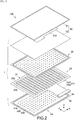
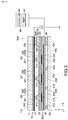
- Fig. 1 is a schematic cross-sectional view of an input device 100 according to a first embodiment of the present disclosure
- Fig. 2 is an exploded perspective view of the input device 100
- Fig. 3 is a schematic cross-sectional view of a main portion of the input device 100
- Fig. 4 is a block diagram of an electronic apparatus 70 using the input device 100.
- an X-axis and a Y-axis represent directions perpendicular to each other (in-plane direction of the input device 100)
- a Z-axis represents a direction perpendicular to the X-axis and the Y-axis (thickness direction or vertical direction of the input device 100).
- the input device 100 includes a flexible display (display element) 11 and a sensor device 1.
- the flexible display 11 receives a user's operation, and the sensor device 1 detects a user's operation.
- the input device 100 is configured as a flexible touch panel display, for example, and is incorporated into the electronic apparatus 70 to be described later.
- the sensor device 1 and the flexible display 11 each have a plate-like shape extending in a direction perpendicular to the Z-axis.
- the flexible display 11 has an input operation surface 110 and a rear surface 120 opposite to the input operation surface 110.
- the flexible display 11 has functions as an input operation unit and a display unit in the input device 100. Specifically, the flexible display 11 causes the input operation surface 110 to function as a display surface, and displays an image on the input operation surface 110 toward the upper side of the Z-axis direction depending on a user's operation. On the input operation surface 110, an image corresponding to a keyboard, GUI (Graphical User Interface), or the like is displayed. Examples of an operation element for performing an operation on the flexible display 11 include a finger, and a pen (stylus pen).
- the specific configuration of the flexible display 11 is not particularly limited.
- the flexible display 11 a so-called electronic paper, an organic EL (Electro Luminescence) panel, an inorganic EL panel, a liquid crystal panel, or the like can be adopted.
- the thickness of the flexible display 11 is not particularly limited, and is about 0.1 mm to 1 mm, for example.
- the sensor device 1 includes a metal film (first conductor layer) 12, a conductor layer (second conductor layer) 50, an electrode substrate 20, a first supporting body 30, and a second supporting body 40.
- the sensor device 1 is disposed on the side of the rear surface 120 of the flexible display 11.
- the metal film 12 is configured to have a sheet-like shape and to be deformable.
- the conductor layer 50 is disposed to face the metal film 12.
- the electrode substrate 20 includes a plurality of first electrode wires 210 and a plurality of second electrode wires 220, is disposed between the metal film 12 and the conductor layer 50 to be deformable, and is capable of electrostatically detecting the change in the distance between the metal film 12 and the conductor layer 50.
- the plurality of second electrode wires 220 are disposed to face the plurality of first electrode wires 210 and intersect with the plurality of first electrode wires 210.
- the first supporting body 30 includes a plurality of first structures 310 and first space portions 330. The plurality of first structures 310 connect the metal film 12 and the electrode substrate 20.
- the first space portions 330 are formed between the plurality of first structures 310.
- the second supporting body 40 includes a plurality of second structures 410 and second space portions 430.
- the respective second structures 410 are disposed between and below adjacent two first structures 310 and connect the conductor layer 50 and the electrode substrate 20.
- the second space portions 430 are formed between the plurality of second structures 410.
- the sensor device 1 electrostatically detects changes in the distance between the metal film 12 and the electrode substrate 20 and the distance between the conductor layer 50 and the electrode substrate 20 due to an input operation on the input operation surface 110 of the flexible display 11, thereby detecting the input operation.
- the input operation is not limited to a conscious pressing (pushing) operation on the input operation surface 110, and may be a contact (touching) operation.
- a conscious pressing (pushing) operation on the input operation surface 110 may be a contact (touching) operation.
- a contact operation can be performed similarly to a general touch sensor.
- the input device 100 includes a controller 60, and the controller 60 includes a calculation unit 61 and a signal generating unit 62.
- the calculation unit 61 detects a user's operation based on the change in capacitance of detection units 20s.
- the signal generating unit 62 generates an operation signal based on the detection results obtained from the calculation unit 61.
- the electronic apparatus 70 shown in Fig 4 includes a controller 710 that performs processing based on the operation signal generated by the signal generating unit 62 in the input device 100.
- the operation signal processed by the controller 710 is output to the flexible display 11 as an image signal, for example.
- the flexible display 11 is connected to a drive circuit mounted on the controller 710 via a flexible wiring substrate 113 (see Fig. 2 ).
- the drive circuit may be mounted on the flexible wiring substrate 113.
- Examples of the electronic apparatus 70 typically include a mobile phone, a smartphone, a laptop PC (Personal Computer), a tablet PC, and a portable game machine.
- the electronic apparatus 70 is not limited to these portable electronic apparatuses or display apparatuses, and may be applied to a stationary electronic apparatus or display apparatus such as an ATM (Automated Teller Machine) and a ticket vending machine.
- ATM Automatic Teller Machine
- the flexible display 11 is configured as a part of an operation member 10 in the input device 100.
- the input device 100 includes the operation member 10, the electrode substrate 20, the first supporting body 30, the second supporting body 40, and the conductor layer 50.
- the operation member 10 has a laminated structure of the flexible display 11 including the input operation surface 110 and the metal film 12. Specifically, the operation member 10 has the input operation surface 110 and the rear surface 120 opposite to the input operation surface 110, and is configured to have a sheet-like shape and to be deformable.
- the input operation surface 110 receives a user's operation, and the metal film 12 is formed on the rear surface 120.
- the metal film 12 is configured to have a sheet-like shape and to be deformable following the deformation of the flexible display 11, and includes metal foil such as Cu (copper) and Al (aluminum), or a mesh material, for example.
- the thickness of the metal film 12 is not particularly limited, and may be about several ten nm to several ten ⁇ m, for example.
- the metal film 12 is connected to a predetermined reference potential (e.g., ground potential). Accordingly, the metal film 12 fulfills a predetermined shielding function against an electromagnetic wave when being mounted on the electronic apparatus 70. Specifically, the metal film 12 prevents an electromagnetic wave from entering from another electronic component mounted on the electronic apparatus 70, and an electromagnetic wave from leaking from the input device 100, for example, thereby contributing to the stability of the operation of the electronic apparatus 70.
- an adhesive layer 13 on which metal foil is formed is attached to the flexible display 11, thereby forming the metal film 12, for example.
- the material of the adhesive layer 13 is not particularly limited as long as it has an adhesive property.
- the adhesive layer 13 may be a resin film to which a resin material is applied.
- the adhesive layer 13 may be configured by a deposition film, a sputtering film, or the like directly formed on the flexible display 11, and may be a coating film such as conductive paste printed on a surface of the flexible display 11.
- the conductor layer 50 forms the lowest portion of the input device 100, and is disposed to face the metal film 12 in the Z-axis direction.
- the conductor layer 50 functions also as a supporting plate of the input device 100, and is configured to have higher bending rigidity than the operation member 10 and the electrode substrate 20, for example.
- the conductor layer 50 may be configured by a metal plate including an Al alloy, a Mg (magnesium) alloy, and another metal material, or a conductor plate such as carbon-fiber reinforced plastic.
- the conductor layer 50 may have a laminated structure in which a plating film, a deposition film, a sputtering film, a conductor film such as metal foil, or the like is formed on an insulating layer including a plastic material.
- the thickness of the conductor layer 50 is not particularly limited, and is about 0.3 mm, for example.
- the conductor layer 50 is connected to a predetermined reference potential (e.g., ground potential). Accordingly, the conductor layer 50 fulfills a function as an electromagnetic shielding layer when being mounted on the electronic apparatus 70. Specifically, the conductor layer 50 prevents an electromagnetic wave from entering from another electronic component mounted on the electronic apparatus 70, and an electromagnetic wave from leaking from the input device 100, for example, thereby contributing to the stability of the operation of the electronic apparatus 70.
- a predetermined reference potential e.g., ground potential
- the electrode substrate 20 includes a wiring substrate 21 having an almost rectangular planar shape.
- the wiring substrate 21 includes the plurality of first electrode wires (X electrodes) 210, the plurality of second electrode wires (Y electrodes) 220 disposed to face the plurality of first electrode wires 210, and a single sheet substrate 211 that supports the plurality of first electrode wires 210 and the plurality of second electrode wires 220.
- the detection units (capacity sensors) 20s are formed in facing areas between the plurality of second electrode wires 220 and the plurality of first electrode wires 210.
- the detection units 20s are arranged in a plane of the electrode substrate 20 in a matrix pattern.
- the sheet substrate 211 includes a sheet material having a flexible property, for example, and specifically includes an electrically-insulating plastic sheet (film) such as poly(ethylene terephthalate) (PET), poly(ethylene naphthalate) (PEN), polycarbonate (PC), poly(methyl methacrylate) (PMMA), and polyimide.
- the thickness of the sheet substrate 211 is not particularly limited, and is several ten ⁇ m to several hundred ⁇ m, for example.
- a substrate obtained by forming an easily-adhesive layer having a thickness of about several 10 nm to several ⁇ m on a surface of a sheet such as PET may be used to obtain an adhesive property at the time of printing or deposition.
- a hard coating layer may be applied to the surface of the sheet in order to prevent the surface being damaged.
- the sheet substrate 211 has a main body 231 and a projecting portion (tale portion) 232.
- the main body 231 has an almost rectangular shape
- the projecting portion 232 has the area smaller than that of the main body 231 and has an almost rectangular shape.
- the sheet substrate 211 is formed by punching processing of a plastic sheet, for example.
- the main body 231 supports the plurality of first electrode wires 210 and the plurality of second electrode wires 220.
- the main body 231 has a first main surface (front surface) 231a that supports the plurality of first electrode wires 210 and a second main surface (rear surface) 231b that supports the plurality of second electrode wires 220.
- Fig. 5 is a schematic plan view of the wiring substrate 21 (schematic plan view viewed from the side of the first main surface 231a of the main body 231)
- Fig. 6 is a schematic rear view of the wiring substrate 21 (schematic plan view viewed from the side of the second main surface 231b of the main body 231).
- the plurality of first electrode wires 210 are arranged at a predetermined interval along the X-axis direction, and are substantially linearly formed along the Y-axis direction.
- the plurality of second electrode wires 220 are arranged at a predetermined interval along the Y-axis direction, and are substantially linearly formed along the X-axis direction. It should be noted that the number of the plurality of first electrode wires 210 and the number of the plurality of second electrode wires 220 are not limited to those shown in the figures, and these electrode wires may be formed more densely.
- the plurality of first electrode wires 210 and the plurality of second electrode wires 220 may each include a single electrode wire, or may each include an electrode wire group formed of a plurality of fine electrode wires. Alternatively, at least one of: the plurality of first electrode wires 210; and the plurality of second electrode wires 220, may be formed so that each intersection area (facing area) is larger than the other respective area. Specifically, the shapes or forms of the plurality of first electrode wires 210 and the plurality of second electrode wires 220 are not particularly limited, and an appropriate shape may be adopted.
- the projecting portion 232 is provided to an edge portion 231e of one long side of the main body 231, and is formed to project outward (in a direction parallel to the Y-axis direction in this example) from the edge portion 231e. Because the projecting portion 232 has a flexible property, the projecting portion 232 is configured to be deformable about the X-axis against the edge portion 231e of the main body 231, for example.
- the projecting portion 232 has a first surface 232a located on the same plane as the first main surface 231a and a second surface 232b located on the same plane as the second main surface 231b.
- the first surface 232a supports a plurality of first lead wires 210s electrically connected to the plurality of first electrode wires 210
- the second surface 232b supports a plurality of second lead wires 220s electrically connected to the plurality of second electrode wires 220.
- the plurality of first lead wires 210s are wiring portions that electrically connect the plurality of first electrode wires 210 and the controller 60, and are formed on the first main surface 231a of the main body 231 and the first surface 232a of the projecting portion 232 to have a predetermined pattern.
- the plurality of second lead wires 220s are wiring portions that electrically connect the plurality of second electrode wires 220 and the controller 60, and are formed on the second main surface 231b of the main body 231 and the second surface 232b of the projecting portion 232 to have a predetermined pattern.
- the electrode substrate 20 further includes a connector component 24.
- the connector component 24 is mounted on the projecting portion 232.
- the position on which the connector component 24 is mounted is not particularly limited, and may be appropriately set depending on the type of the connector component 24 or the form of the first lead wires 210s and the second lead wires 220s.
- the connector component 24 is typically mounted on an end portion of the projecting portion 232.
- the connector component 24 is configured to electrically and mechanically connect the electrode substrate 20 and the controller 60. Therefore, the connector component 24 is not necessarily provided to the electrode substrate 20 and may be provided to the controller 60 (circuit substrate constituting the controller 60).
- the plurality of first electrode wires 210, the plurality of second electrode wires 220, the plurality of first lead wires 210s, and the plurality of second lead wires 220s may be formed by a printing method such as screen printing, gravure offset printing, and inkjet printing, using conductive paste or the like, or by a patterning method using a photolithography technique with metal foil or a metal layer.
- the plurality of first electrode wires 210 and the plurality of second electrode wires 220 are disposed to be apart from each other in the thickness direction of the sheet substrate 211 (Z-axis direction). Therefore, in the electrode substrate 20, the detection units (capacity sensors) 20s formed in the facing areas of the plurality of first electrode wires 210 and the plurality of second electrode wires 220 are arranged in a matrix pattern. The detection units 20s are formed in the intersection areas of the plurality of first electrode wires 210 and the plurality of second electrode wires 220.
- the controller 60 is electrically connected to the electrode substrate 20. Specifically, the controller 60 is connected to the first electrode wires 210 and the second electrode wires 220 via terminals.
- the controller 60 constitutes a signal processing circuit that is capable of generating information on the input operation on the input operation surface 110 based on output from the detection units 20s.
- the controller 60 acquires the amount of change in the capacity of the detection units 20s while scanning the detection units 20s at a predetermined cycle.
- the controller 60 generates information on the input operation based on the capacity change amount.
- the controller 60 is typically formed of a computer including a CPU (Central Processing Unit) or MPU (Microprocessor Unit), and a memory.
- the controller 60 may include a single chip component, or a plurality of circuit components.
- the controller 60 may be mounted on the input device 100, or on the electronic apparatus 70 into which the input device 100 is incorporated. In the former case, the controller 60 is mounted on a flexible wiring substrate connected to the electrode substrate 20, for example. In the latter case, the controller 60 may be integrally formed with the controller 710 that controls the electronic apparatus 70.
- the controller 60 includes the calculation unit 61 and the signal generating unit 62 as described above, and executes various functions in accordance with a program stored in storage (not shown).
- the calculation unit 61 calculates the operation position in the XY coordinate system on the input operation surface 110 based on an electrical signal (input signal) output from the first electrode wires 210 and the second electrode wires 220 on the electrode substrate 20.
- the signal generating unit 62 generates an operation signal based on the calculation results. Accordingly, an image based on an input operation on the input operation surface 110 can be displayed on the flexible display 11.
- the calculation unit 61 shown in Figs. 3 and 4 calculates the XY coordinate pair of the operation position of an operation element on the input operation surface 110 based on output from the respective detection units 20s to which a unique XY coordinate pair is assigned. Specifically, the calculation unit 61 calculates the amount of change in the capacitance in the detection units 20s formed in the intersection areas (facing areas) of the X electrodes (first electrode wires 210) and the Y electrodes (second electrode wires 220) based on the amount of change in the capacitance acquired from the X electrodes and the Y electrodes. With the ratio of the amount of change in the capacitance of the detection units 20s or the like, it is possible to calculate the XY coordinate pair of the operation position of the operation element.
- the calculation unit 61 is capable of determining whether or not the input operation surface 110 is operated. Specifically, in the case where the value of the amount of change in the capacitance of the entire detection units 20s or the amount of change in the capacitance of the respective detection units 20s is not less than a predetermined threshold value, for example, it is possible to determine that the input operation surface 110 is operated. In addition, by providing two or more threshold values, it is possible to distinguish a touching operation from a (conscious) pushing operation for performing the determination, for example. Furthermore, it is also possible to calculate a pressing force based on the amount of change in the capacitance of the detection units 20s.
- the signal generating unit 62 generates a predetermined operation signal based on the calculation results obtained from the calculation unit 61.
- the operation signal may be an image control signal for generating a display image to be output to the flexible display 11, an operation signal corresponding to a key in a keyboard image displayed on the operation position on the flexible display 11, or an operation signal related to an operation corresponding to a GUI (Graphical User Interface).
- the input device 100 includes the first supporting body 30 and the second supporting body 40 as a configuration in which the distance between the metal film 12 and the electrode substrate 20 (detection units 20s) and the distance between the conductor layer 50 and the electrode substrate 20 are changed by an operation on the input operation surface 110.
- the first supporting body 30 and the second supporting body 40 will be described.
- the first supporting body 30 is disposed between the operation member 10 and the electrode substrate 20.
- the first supporting body 30 includes the plurality of first structures 310, a plurality of frame bodies 320, and the first space portions 330.
- the first supporting body 30 is joined above the electrode substrate 20 via an adhesive layer 35 (see Fig. 3 ).
- the adhesive layer 35 may include an adhesive agent or an adhesive material such as a pressure-sensitive adhesive and a pressure-sensitive tape.
- the first supporting body 30 has a laminated structure of a substrate 31, a structure layer 32 provided on a surface (upper surface) of the substrate 31, and a plurality of joining portions 341 formed on a predetermined position on the structure layer 32.
- the substrate 31 includes an electrically-insulating plastic sheet such as PET, PEN, and PC (polycarbonate).
- the thickness of the substrate 31 is not particularly limited, and is several ⁇ m to several hundred ⁇ m, for example.
- the structure layer 32 includes an electrically-insulating resin material such as UV resin, and forms, on the substrate 31, a plurality of first convex portions 321, a plurality of second convex portions 322, and a plurality of concave portions 323.
- the plurality of first convex portions 321 each have a shape such as a columnar shape, rectangular column shape, and a frustum shape that projects in the Z-axis direction, and are arranged on the substrate 31 at a predetermined interval, for example.
- the plurality of second convex portions 322 are formed to surround the substrate 31 and have a predetermined width.
- the structure layer 32 includes a material having enough rigidity to deform the electrode substrate 20 by an input operation on the input operation surface 110.
- the structure layer 32 may include an elastic material that can be deformed together with the operation member 10 at the time of the input operation.
- the modulus of elasticity of the structure layer 32 is not particularly limited, and may be appropriately selected in the range in which desired operation feeling or detection sensitivity is acquired.
- the plurality of concave portions 323 are formed to have a flat surface between the plurality of first convex portions 321 and the plurality of second convex portions 322. Specifically, space areas on the plurality of concave portions 323 form the first space portions 330. Moreover, an adhesion prevention layer 342 (not shown in Fig. 3 ) including UV resin with a low adhesive property is formed on the plurality of concave portions 323.
- the shape of the adhesion prevention layer 342 is not particularly limited.
- the adhesion prevention layer 342 may be formed to have an island shape, or may be formed to be a flat layer on the plurality of concave portions 323.
- the plurality of joining portions 341 including an adhesive resin material or the like are formed on the plurality of first convex portions 321 and the plurality of second convex portions 322.
- the plurality of first structures 310 are formed to have laminated bodies of the plurality of first convex portions 321 and the plurality of joining portions 341 formed thereon
- the frame bodies 320 include laminated bodies of the plurality of second convex portions 322 and the plurality of joining portions 341 formed thereon. Accordingly, the plurality of first structures 310 and the frame bodies 320 are formed to have almost the same thickness (height), e.g., several ⁇ m to several hundred ⁇ m.
- the height of the adhesion prevention layer 342 is not particularly limited as long as it is lower than the height of the plurality of first structures 310 and the frame bodies 320, and the adhesion prevention layer 342 is formed to be lower than the plurality of first convex portions 321 and the plurality of second convex portions 322, for example.
- the plurality of first structures 310 are disposed to correspond to the arrangement of the detection units 20s.
- the plurality of first structures 310 are disposed to face the center of the detection units 20s in the Z-axis direction, for example.
- the plurality of first structures 310 are not limited thereto, and may be disposed on positions offset from the center of the detection units 20s.
- the number of first structures 310 that face the respective detection units 20s is not limited to one, and may be two or more.
- the frame bodies 320 are formed to surround the first supporting body 30 along the rim of the electrode substrate 20.
- the length of the frame bodies 320 in a short direction, i.e., width, is not particularly limited as long as the strength of the first supporting body 30 and the entire input device 100 can be sufficiently ensured.
- the second supporting body 40 is disposed between the electrode substrate 20 and the conductor layer 50.
- the second supporting body 40 includes the plurality of second structures 410, second frame bodies 420, and the second space portions 430.
- the second supporting body 40 As shown in Fig. 3 , in the second supporting body 40, the plurality of second structures 410 and the second frame bodies 420 are directly formed on the conductor layer 50.
- the second supporting body 40 is joined under the electrode substrate 20 via an adhesive layer 36 (see Fig. 3 ).
- the adhesive layer 36 may include an adhesive agent or an adhesive material such as a pressure-sensitive adhesive and a pressure-sensitive tape. Alternatively, the adhesive layer 36 may be omitted as necessary.
- the plurality of second structures 410 and the second frame bodies 420 include an adhesive insulating resin material, for example, and function also as a joining portion that joins the conductor layer 50 to the electrode substrate 20.
- the thickness of the plurality of second structures 410 and the second frame bodies 420 is not particularly limited, and is several ⁇ m to several hundred ⁇ m for example.
- the respective second structures 410 are disposed between and below adjacent two first structures 310. That is, the respective second structures 410 are disposed between and below adjacent two detection units 20s.
- the plurality of second structures 410 are not limited thereto, and may be disposed to face the detection units 20s.
- the second frame bodies 420 are formed to surround the second supporting body 40 along the rim of the conductor layer 50.
- the width of the second frame bodies 420 is not particularly limited as long as the strength of the second supporting body 40 and the entire input device 100 can be sufficiently ensured.
- the second frame bodies 420 are formed to have almost the same width as that of the frame bodies 320.
- the modulus of elasticity of the plurality of second structures 410 is not particularly limited similarly to the structure layer 32 constituting the plurality of first structures 310. Specifically, the modulus of elasticity of the plurality of second structures 410 may be appropriately selected in the range in which desired operation feeling or detection sensitivity is acquired, and the plurality of second structures 410 may include an elastic material that can be deformed together with the electrode substrate 20 at the time of the input operation.
- the respective second space portions 430 are formed between two second structures 410, and form space areas around the plurality of second structures 410 and the second frame bodies 420.
- the second space portions 430 receive the detection units 20s and the plurality of first structures 310 when viewed from the Z-axis direction.
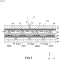
- Fig. 7 is a schematic cross-sectional view showing the force applied to the first structures 310 and the second structures 410 when a point P on the input operation surface 110 is pressed downward in the Z-axis direction by an operation element h.
- Solid-white arrows in Fig. 7 schematically show the magnitude of the downward force in the Z-axis direction (hereinafter, referred to as simply "downward").
- the form of the deflection of the metal film 12, the electrode substrate 20, and the like, an elastic deformation of the first structures 310, or the second structures 410 is not shown. It should be noted that in the following description, because a small pressing force is actually applied even if a user performs a touching operation with no conscious pressing, these input operations are collectively referred to as "pressing.”
- first structures 310p1 and 310p2 adjacent to the first space portion 330p0 receive a force F1, and are elastically deformed in the Z-axis direction, thereby reducing the thickness.
- a first structure 310p3 adjacent to the first structure 310p1 and a first structure 310p4 adjacent to the first structure 310p2 receive a force F2 smaller than F1.
- a force is applied to the electrode substrate 20 due to the forces F1 and F2, thereby deflecting mainly areas located immediately below the first structures 310p1 and 310p2 downward.
- a second structure 410p0 disposed between the first structures 310p1 and 310p2 receives a force F3, and the second structure 410p0 is elastically deformed in the Z-axis direction, thereby reducing the thickness.
- a second structure 410p1 disposed between and below the first structures 310p1 and 310p3 and a second structure 410p2 disposed between and below the first structures 310p2 and 310p4 receive a force F4 smaller than F3.
- the metal film 12 and the electrode substrate 20 are deflected, and an influence of a pressing force is exerted in the in-plane direction (direction parallel to the X-axis direction and the Y-axis direction), thereby exerting an influence of a pressing force not only on the area located immediately below the operation element h but also on the first structures 310 and the second structures 410 in the vicinity thereof.
- the metal film 12 and the electrode substrate 20 can be easily deformed with the first space portions 330 and the second space portions 430. Furthermore, it is possible to apply high pressure to the electrode substrate 20 by the pressing force of the operation element h with the first structures 310 and the second structures 410 having a pillar shape or the like, thereby deflecting the electrode substrate 20 efficiently. Because the electrode substrate 20 is formed of the wiring substrate 21 including the single sheet substrate 211, it is possible to enhance the deformability.
- the plurality of first structures 310 easily deflect the electrode substrate 20 via the second space portions 430 located therebelow.
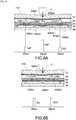
- Figs. 8A and 8B are each a schematic main portion cross-sectional view showing the state of the input device 100 when the input operation surface 110 is operated by the operation element h, and show an exemplary signal output from the detection units 20s at that time. Bar graphs shown along the X-axis in Figs. 8A and 8B schematically show the amount of change in the capacitance from the reference value in the detection units 20s.
- Fig. 8A shows the state where the first structures 310 (310a2) is pressed by the operation element h
- Fig. 8B shows the state where the first space portion 330 (330b1) is pressed by the operation element h.
- a force is applied most to the first structure 310a2 located immediately below the operation position and the first structure 310a2 itself is elastically deformed and displaced downward. Due to the displacement, a detection unit 20sa2 located immediately below the first structure 310a2 is displaced downward. Accordingly, the detection unit 20sa2 and the conductor layer 50 come close to each other via a second space portion 430a2. Specifically, the distance between the detection unit 20sa2 and the metal film 12 is slightly changed and the distance between the detection unit 20sa2 and the conductor layer 50 is greatly changed. Accordingly, the detection unit 20sa2 acquires an amount of change in the capacitance Ca2.
- first structures 310a1 and 310a3 are slightly displaced downward, and the amounts of changes in the capacitances of detection units 20sal and 20sa3 are Ca1 and Ca3, respectively.
- the amount of change in the capacitance Ca2 is the largest, and the amounts of change in the capacitance Ca1 and Ca3 are almost the same and smaller than the amount of change in the capacitance Ca2.
- the amounts of change in the capacitance Ca1, Ca2, and Ca3 show unimodal distribution with the amount of change in the capacitance Ca2 being a vertex.
- the calculation unit 61 is capable of calculating the center of gravity or the like based on the ratio of the amounts of change in the capacitance Ca1, Ca2, and Ca3, and calculating the XY coordinate pair on the detection unit 20sa2 as the operation position.
- first structures 310b1 and 310b2 in the vicinity of the operation position are elastically deformed slightly and displaced downward due to the deflection of the metal film 12. Due to the displacement, the electrode substrate 20 is deflected, and detection units 20sb1 and 20sb2 located immediately below the first structures 310b1 and 310b2 are displaced downward. Accordingly, the detection units 20sb1 and 20sb2 come close to the conductor layer 50 via second space portions 430b1 and 430b2.
- the distance between the detection units 20sb1 and 20sb2 and the metal film 12 is slightly changed, the distance between the detection units 20sb1 and 20sb2 and the conductor layer 50 is relatively largely changed, and thus amounts of change in the capacitance Cb1 and Cb2 are obtained, respectively.
- the calculation unit 61 is capable of calculating the XY coordinate pair between the detection units 20sb1 and 20sb2 as the operation position.
- the thickness between the detection units 20s and the metal film 12 and the thickness between the detection units 20s and the conductor layer 50 are variable by a pressing force, it is possible to make the mount of change in the capacitance in the detection units 20s large. Accordingly, it is possible to improve the detection sensitivity of the input operation.
- the operation position on the flexible display 11 is on any point on the plurality of first structures 310 or the first space portions 330, it is possible to calculate the XY coordinate pair of the operation position.
- the metal film 12 causes an influence of a pressing force to exert in the in-plane direction, it is possible to change the capacitance of not only the detection units 20s located immediately below the operation position but also the detection units 20s in the vicinity of the operation position when viewed from the Z-axis direction. Accordingly, it is possible to reduce the variety of the detection accuracy in the input operation surface 110 and to maintain high detection accuracy on the entire surface of the input operation surface 110.
- the electrode substrate 20 has a configuration in which the first electrode wires 210 and the second electrode wires 220 are provided on both surface of the single sheet substrate 211, it is possible to improve the deformation property of the electrode substrate 20 as compared with the case where the electrode substrate 20 includes a laminated body of two wiring substrates that support the electrode wires, for example. Accordingly, it is possible to improve the sensitivity of the detection units 20s and to further improve the detection accuracy.
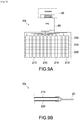
- Fig. 9A is a plan view of an electrode substrate 20r according to a comparative example
- Fig. 9B is a main portion cross-sectional side view.
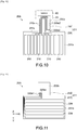
- Fig. 10 and Fig. 11 are a plan view and a rear view of the electrode substrate 20 in the input device (sensor device), respectively.
- configurations that are different from those according to the first embodiment will be mainly described, the same configurations as those according to the embodiment will be denoted by the same reference symbols, and a description thereof will be omitted or simplified.
- Fig. 10 is a plan view of an electrode substrate 20A and Fig. 11 is a rear view thereof.
- the electrode substrate 20A includes the single sheet substrate 211 having the main body 231 and the projecting portion 232 similarly to the first embodiment. Then, the electrode substrate 20A according to this embodiment is different from that in the first embodiment in that the plurality of second lead wires 220s connected to the plurality of second electrode wires 220 are formed from the second surface 232b of the projecting portion 232 to the first surface 232a.
- the plurality of second lead wires 220s include a plurality of first wiring portions 220s1 formed on the second surface 232b of the projecting portion 232, a plurality of second wiring portions 220s2 formed on the first surface 232a of the projecting portion 232, and a plurality of vias 220sv that connect the plurality of first wiring portions 220s1 and the plurality of second wiring portions 220s2 to each other.
- the plurality of vias 220sv each correspond to an interlayer connection portions that pass through the projecting portion 232, and typically include an embedded via, through-hole plating, or the like.
- the same operation and effect as those according the first embodiment can be obtained.
- the first lead wires 210s and the second lead wires 220s can be pulled out to the first surface 232a of the projecting portion 232, it is possible to improve the degree of freedom of mounting to the connector component 24 or the controller 60.
- a plurality of first electrode wires and a plurality of second electrode wires are separated from each other in the thickness direction of an electrode substrate, and a plurality of detection units (capacity sensors) are formed in intersection areas of these electrode wires.
- a plurality of first electrode wires and a plurality of second electrode wires are separated from each other in the plane of an electrode substrate, and a plurality of detection units (capacity sensors) are formed in facing areas of these electrode wires.
- Fig. 12A is a schematic cross-sectional view of an input device 100C and Fig. 12B is a cross-sectional view showing an enlarged main portion of the input device 100C.
- This embodiment is different from the first embodiment in that an electrode substrate 20C electrostatically detects the change in the distance between the electrode substrate 20C and the metal film 12 and the distance between the electrode substrate 20C and the conductor layer 50 by the amount of change in the capacitive coupling in the XY plane.
- Y electrodes 220C include facing portions that face X electrodes 210C in the in-plane direction of the electrode substrate 20C, and the facing portions form detection units 20Cs.
- the electrode substrate 20C includes a sheet substrate 211C on which the plurality of first electrode wires (X electrodes) 210C and the plurality of second electrode wires (Y electrodes) 220C are disposed, and these plurality of X electrodes 210C and the plurality of Y electrodes 220C are disposed on the same plane (same main surface) of the sheet substrate 211C.
- the exemplary configuration of the X electrodes (first electrode wires) 210C and the Y electrodes (second electrode wires) 220C will be described.
- the respective X electrodes 210C and the respective Y electrodes 220C include a plurality of pectinate unit electrode bodies (first unit electrode bodies) 210m and a plurality of unit electrode bodies (second unit electrode bodies) 220m, and one unit electrode body 210m and one unit electrode body 220m form the respective detection units 20Cs will be described.
- the respective X electrodes 210C include the plurality of unit electrode bodies 210m, an electrode wire portion 210p, and a plurality of connection portions 210z.
- the electrode wire portion 210p extends in the Y-axis direction.
- the plurality of unit electrode bodies 210m are disposed at predetermined intervals in the Y-axis direction.
- the electrode wire portion 210p and the unit electrode bodies 210m are arranged at a predetermined interval, and are connected by the connection portions 210z.
- the entire unit electrode bodies 210m have a pectinate shape.
- the unit electrode bodies 210m include a plurality of sub-electrodes 201w and coupling portions 210y.
- the plurality of sub-electrodes 210w extend in the X-axis direction. Adjacent two sub-electrodes 210w are apart from each other at a predetermined interval. An end of the respective sub-electrodes 210w is connected to the coupling portion 210y extending in the X-axis direction.
- the Y electrodes 220C includes the plurality of unit electrode bodies 220m, electrode wire portions 220p, and a plurality of connection portions 220z.
- the electrode wire portions 220p extend in the X-axis direction.
- the plurality of unit electrode bodies 220m are disposed at predetermined intervals in the X-axis direction.
- the electrode wire portions 220p and the unit electrode bodies 220m are disposed to be apart from each other at a predetermined interval, and are connected by the connection portions 220z. It should be noted that it may be possible to employ a configuration in which the connection portions 220z are omitted and the unit electrode bodies 220m are directly provided on the electrode wire portions 220p.
- the entire unit electrode bodies 220m have a pectinate shape.
- the unit electrode bodies 220m include a plurality of sub-electrodes 220w and a coupling portion 220y.
- the plurality of sub-electrodes 220w extend in the X-axis direction. Adjacent two sub-electrodes 220w are apart from each other at a predetermined interval. An end of the respective sub-electrodes 220w is connected to the coupling portion 220y extending in the Y-axis direction.
- the detection units 20Cs are formed in areas in which the unit electrode bodies 210m and the unit electrode bodies 220m are combined with each other.
- the plurality of sub-electrodes 210w of the unit electrode bodies 210m and the plurality of sub-electrodes 220w of the unit electrode bodies 220m are alternately arranged toward the Y-axis direction.
- the sub-electrodes 210w and 220w are arranged to face each other in the in-plane direction of the electrode substrate 20C (e.g., Y-axis direction).
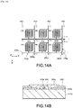
- Fig. 14B is a cross-sectional view when viewed from the A-A direction of Fig. 14A .
- the Y electrodes 220C are provided to intersect the X electrodes 210C but are formed on the same plane (same main surface of the sheet substrate 211C) as that of the X electrodes 210C.
- areas in which the X electrodes 210C and the Y electrodes 220C intersect with each other are formed so that the X electrodes 210C and the Y electrodes 220C are not directly brought into contact with each other.
- an insulating layer 220r is provided on the electrode wire portions 210p of the X electrodes 210C and the electrode wire portions 220p of the Y electrodes 220C. Then, in an area in which the X electrodes 210C and the Y electrodes 220C intersect with each other, a jumper wiring portion 220q is provided to bridge the insulating layer 220r. The jumper wiring portion 220q connects the electrode wire portions 220p with each other.
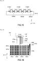
- Fig. 15 is a schematic cross-sectional view for explaining the configuration of the detection units 20Cs.
- a sub-electrode 210w1 and a sub-electrode 220w1 and 210w1 the sub-electrode 220w1 and 210w2
- the sub-electrode 210w2 and a sub-electrode 220w2 the sub-electrode 220w2 and a sub-electrode 210w3
- the sub-electrode 210w3 and a sub-electrode 220w3 are capacitively-coupled, respectively.
- capacitances Cc11, Cc12, Cc13, Cc14, and Cc15 between the respective sub-electrodes are variable depending on the capacitive coupling of the metal film 12 and the conductor layer 50 with the first electrode wires 210C and the second electrode wires 220C including the sub-electrodes with the sheet substrate 211C being as a dielectric layer.
- Fig. 16 is a schematic plan view of the electrode substrate 20C.
- the sheet substrate 211C has the main body 231 and the projecting portion 232 and the projecting portion 232 is formed to project outward from one edge portion 231e of the main body 231.
- the plurality of first electrode wires 210C and the plurality of second electrode wires 220C are formed on the first main surface 231a of the sheet substrate 211C.
- the plurality of first lead wires 210s connected to the plurality of first electrode wires 210C and the plurality of second lead wires 220s connected to the plurality of second electrode wires 220C are formed on the first main surface 231a of the main body 231 and the first surface 232a of the projecting portion 232, respectively.
- the configuration it is possible to obtain the same operation and effect as those in the first embodiment. Moreover, many sub-electrodes are capacitively-coupled, and the distance between the capacitively-coupled sub-electrodes can be narrowed. Accordingly, it is possible to increase the amount of capacitive coupling of the entire input device 100C and to improve the detection sensitivity.
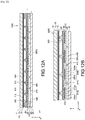
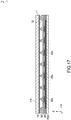
- Fig. 17 shows the exemplary configuration of the input device in which the second supporting body 40 is omitted
- Fig. 18 shows the exemplary configuration of the input device in which the first supporting body 30 is omitted, respectively.
- a supporting layer 50A including an insulating material may be used instead of the conductor layer 50.
- the electrode substrate 20 is fixed to the supporting layer 50A, and the input position and the pressing force are detected based on the change in the distance between the metal film 12 and the detection units 20s at the time of input operation to the input operation surface 110.
- the metal film 12 on the side of the operation member 10 may be unnecessary.
- the electrode substrate 20 is fixed to the operation member 10, and the input position and the pressing force are detected based on the change in the distance between the conductor layer 50 and the detection units 20s at the time of input operation to the input operation surface 110.
Description
- This application claims the benefit of Japanese Priority Patent Application
JP 2013-187049 filed September 10, 2013 - The present disclosure relates to a sensor device, an input device, and an electronic apparatus that are capable of electrostatically detecting an input operation.
- A sensor device for an electronic apparatus, which includes a capacitive element and is capable of detecting an operation position and a pressing force of an operation element on the input operation surface, for example, has been known (see, for example, Patent Literature 1).
- PTL 1: Japanese Patent Application Laid-open No.
2011-170659 -
US2011/0181548A1 discloses a capacitively coupling type touch panel, including a plurality of coordinate detection electrodes for detecting X-Y position coordinates, a first substrate including the plurality of coordinate detection electrodes and a second substrate disposed to be opposed to the first substrate. -
US2001/0090175A1 discloses another capacitively coupling type touch panel, including a plurality of coordinate detection electrodes for detecting X-Y position coordinates, a first substrate including the plurality of coordinate detection electrodes and a second substrate disposed to be opposed to the first substrate. -
EP2544081A2 discloses a position detecting sensor configured by providing a dielectric member having flexibility between first conductors and second conductors and providing spacers for separating the first conductors or the second conductors from the dielectric member by a determined gap. -
US2008/0202251A1 discloses a capacitive pressure which comprises a laminated arrangement with a first flexible, electrically insulating carrier film carrying a first capacitor electrode, a second flexible, electrically insulating carrier film carrying a second capacitor electrode and a flexible, electrically insulating spacer film sandwiched between the first and second carrier films. -
US8063886B2 discloses a data input device with a film-based pressure sensor including a first carrier film, a second carrier film and a spacer. - In recent years, an input method that uses a gesture operation with a finger and has a high degree of freedom has been performed. Moreover, if a pressing force on an operation surface can be reliably detected with high accuracy, various input operations are expected to be performed. In addition, with the thickness reduction of an electronic apparatus in recent years, an input device is expected to be reduced in thickness.
- In view of the circumstances as described above, it is desirable to provide a sensor device, an input device, and an electronic apparatus that are capable of reliably detecting a pressing force on an operation surface with high accuracy and are suitable for thickness reduction.
- In an embodiment, a sensor device is provided as set out in the independent claim.
- In another example, an input device includes an operating member having an input operation surface, a sheet-like first conductor layer that supports the operating member, and an electrode substrate. The electrode substrate includes a plurality of first electrode wires, a plurality of second electrode wires, capacity sensors being formed at paired portions of the first and second electrode wires, and a sheet substrate that supports the first and second electrode wires. The input device further includes a first supporting body including a plurality of first structures that connect the first conductor layer and the electrode substrate.
- In another example, an electronic apparatus includes a display element having an input operation surface, a sheet-like first conductor layer that supports the display element, and an electrode substrate. The electrode substrate includes a plurality of first electrode wires, a plurality of second electrode wires, capacity sensors being formed at paired portions of the first and second electrode wires, and a sheet substrate that supports the first and second electrode wires. The electronic apparatus also includes a first supporting body including a plurality of first structures that connect the first conductor layer and the electrode substrate.
- According to an example of the present disclosure, there is provided a sensor device including a first conductor layer, an electrode substrate, and a first supporting body. The first conductor layer is formed to be sheet-like and to be deformable. The electrode substrate includes a plurality of first electrode wires, a plurality of second electrode wires disposed to face the plurality of first electrode wires, capacity sensors being formed in facing areas between the plurality of second electrode wires and the plurality of first electrode wires, respectively, and a single sheet substrate that supports the plurality of first electrode wires and the plurality of second electrode wires. The first supporting body includes a plurality of first structures that connect the first conductor layer and the electrode substrate.
- In the sensor device, the relative distance between the first conductor layer and the electrode substrate is changed when the first conductor layer is pressed, and an input operation such as pressing can be electrostatically detected based on the change in the relative distance. Accordingly, it is possible to reliably detect a pressing force on an operation surface with high accuracy. In addition, because the first electrode wires and the second electrode wires are supported on the single sheet substrate, the electrode substrate can be made thin. Accordingly, it is possible to make the sensor device thin.
- The sheet substrate may have a main body and a projecting portion. The main body supports the plurality of first electrode wires and the plurality of second electrode wires. The projecting portion is provided on an edge portion of the main body, projects outward from the edge portion, and supports a plurality of first lead wires and a plurality of second lead wires connected to the plurality of first electrode wires and the plurality of second electrode wires, respectively.
- The main body may have a first main surface that supports the plurality of first electrode wires, and a second main surface that supports the plurality of second electrode wires. The projecting portion may have a first surface that supports the plurality of first lead wires, and a second surface that supports the plurality of second lead wires.
- The plurality of second lead wires may have a plurality of first wiring portions formed on the second surface, a plurality of second wiring portions formed on the first surface, and a plurality of via portions that connect the plurality of first wiring portions and the plurality of second wiring portions and pass through the projecting portion.
- The plurality of first electrode wires and the plurality of second electrode wires may be formed on the same main surface of the main body.
- The electrode substrate may further include a connector component mounted on the projecting portion. The connector component may be electrically connected to the plurality of first lead wires and the plurality of second lead wires.
- The sensor device may further include a second conductor layer and a second supporting body. The second conductor layer is disposed to face the first conductor layer with the electrode substrate disposed therebetween. The second supporting body includes a plurality of second structures that connect the second conductor layer and the electrode substrate.
- According to an example of the present disclosure, there is provided an input device including an operating member, a first conductor layer, an electrode substrate, and a first supporting body. The operating member has an input operation surface. The first conductor layer is formed to be sheet-like, to support the operating member, and to be deformable. The electrode substrate includes a plurality of first electrode wires, a plurality of second electrode wires disposed to face the plurality of first electrode wires, capacity sensors being formed in facing areas between the plurality of second electrode wires and the plurality of first electrode wires, respectively, and a single sheet substrate that supports the plurality of first electrode wires and the plurality of second electrode wires. The first supporting body includes a plurality of first structures that connect the first conductor layer and the electrode substrate.
- According to an example of the present disclosure, there is provided an electronic apparatus including a display element, a first conductor layer, an electrode substrate, and a first supporting body. The display element has an input operation surface. The first conductor layer is formed to be sheet-like, to support the display element, and to be deformable. The electrode substrate includes a plurality of first electrode wires, a plurality of second electrode wires disposed to face the plurality of first electrode wires, capacity sensors being formed in facing areas between the plurality of second electrode wires and the plurality of first electrode wires, respectively, and a single sheet substrate that supports the plurality of first electrode wires and the plurality of second electrode wires. The first supporting body includes a plurality of first structures that connect the first conductor layer and the electrode substrate.
- As described above, according to the present disclosure, it is possible to reliably detect a pressing force on an operation surface with high accuracy and to make a sensor device thin. It should be noted that the effects described here are not necessarily limited, and may be any one of the effects described in the present disclosure.
-
- [
fig. 1] Fig. 1 is a schematic cross-sectional view of an input device. - [
fig. 2] Fig. 2 is an exploded perspective view of the input device. - [
fig. 3] Fig. 3 is a schematic cross-sectional view of a main portion of the input device. - [
fig. 4] Fig. 4 is a block diagram of an electronic apparatus using the input device. - [
fig. 5] Fig. 5 is a schematic plan view of an electrode substrate in the input device. - [
fig. 6] Fig. 6 is a schematic rear view of the electrode substrate. - [
fig. 7] Fig. 7 is a schematic cross-sectional view showing the force applied to first and second structures when a point of a first surface of the input device described above is pressed downward in a Z-axis direction by an operation element. - [
fig. 8] Figs. 8 are each a schematic main portion cross-sectional view showing the state of the input device when a point of the first surface above the first structure is operated by an operation element, and show an exemplary signal output from a detection unit at that time. - [
Fig. 9] Figs. 9 are each a schematic configuration diagram of an electrode substrate according to a comparative example,Fig. 9A is a plan view, andFig. 9B is a main portion cross-sectional side view. - [
fig. 10] Fig. 10 is a schematic plan view of an electrode substrate in the input device. - [
fig. 11] Fig. 11 is a schematic rear view of the electrode substrate. - [
fig. 12] Fig. 12A is a schematic cross-sectional view of an input device andFig. 12B is a cross-sectional view showing an enlarged main portion of the input device. - [
fig. 13] Figs. 13 are each a main portion plan view showing the configuration of first electrode wires and second electrode wires in the input device. - [
fig. 14] Fig. 14A is a plan view of a main portion of an electrode substrate in the input device, andFig. 14B is a cross-sectional view taken along the line A-A ofFig. 14A . - [
fig. 15] Fig. 15 is a schematic cross-sectional view for explaining the configuration of a detection unit in the input device. - [
fig. 16] Fig. 16 is a schematic plan view of the electrode substrate. - [
fig. 17] Fig. 17 is a schematic cross-sectional view showing a modified example of the configuration of the input device. - [
fig. 18] Fig. 18 is a schematic cross-sectional view showing a modified example of the configuration of the input device. - Hereinafter, embodiments and examples not covered by the claims of the present disclosure will be described with reference to the drawings.
-
Fig. 1 is a schematic cross-sectional view of aninput device 100 according to a first embodiment of the present disclosure,Fig. 2 is an exploded perspective view of theinput device 100,Fig. 3 is a schematic cross-sectional view of a main portion of theinput device 100, andFig. 4 is a block diagram of anelectronic apparatus 70 using theinput device 100. Hereinafter, the configuration of theinput device 100 will be described. It should be noted that in the figures, an X-axis and a Y-axis represent directions perpendicular to each other (in-plane direction of the input device 100), and a Z-axis represents a direction perpendicular to the X-axis and the Y-axis (thickness direction or vertical direction of the input device 100). - The
input device 100 includes a flexible display (display element) 11 and asensor device 1. Theflexible display 11 receives a user's operation, and thesensor device 1 detects a user's operation. Theinput device 100 is configured as a flexible touch panel display, for example, and is incorporated into theelectronic apparatus 70 to be described later. Thesensor device 1 and theflexible display 11 each have a plate-like shape extending in a direction perpendicular to the Z-axis. - The
flexible display 11 has aninput operation surface 110 and arear surface 120 opposite to theinput operation surface 110. Theflexible display 11 has functions as an input operation unit and a display unit in theinput device 100. Specifically, theflexible display 11 causes theinput operation surface 110 to function as a display surface, and displays an image on theinput operation surface 110 toward the upper side of the Z-axis direction depending on a user's operation. On theinput operation surface 110, an image corresponding to a keyboard, GUI (Graphical User Interface), or the like is displayed. Examples of an operation element for performing an operation on theflexible display 11 include a finger, and a pen (stylus pen). - The specific configuration of the
flexible display 11 is not particularly limited. For example, as theflexible display 11, a so-called electronic paper, an organic EL (Electro Luminescence) panel, an inorganic EL panel, a liquid crystal panel, or the like can be adopted. In addition, the thickness of theflexible display 11 is not particularly limited, and is about 0.1 mm to 1 mm, for example. - The
sensor device 1 includes a metal film (first conductor layer) 12, a conductor layer (second conductor layer) 50, anelectrode substrate 20, a first supportingbody 30, and a second supportingbody 40. Thesensor device 1 is disposed on the side of therear surface 120 of theflexible display 11. - The
metal film 12 is configured to have a sheet-like shape and to be deformable. Theconductor layer 50 is disposed to face themetal film 12. Theelectrode substrate 20 includes a plurality offirst electrode wires 210 and a plurality ofsecond electrode wires 220, is disposed between themetal film 12 and theconductor layer 50 to be deformable, and is capable of electrostatically detecting the change in the distance between themetal film 12 and theconductor layer 50. The plurality ofsecond electrode wires 220 are disposed to face the plurality offirst electrode wires 210 and intersect with the plurality offirst electrode wires 210. The first supportingbody 30 includes a plurality offirst structures 310 andfirst space portions 330. The plurality offirst structures 310 connect themetal film 12 and theelectrode substrate 20. Thefirst space portions 330 are formed between the plurality offirst structures 310. The second supportingbody 40 includes a plurality ofsecond structures 410 andsecond space portions 430. The respectivesecond structures 410 are disposed between and below adjacent twofirst structures 310 and connect theconductor layer 50 and theelectrode substrate 20. Thesecond space portions 430 are formed between the plurality ofsecond structures 410. - The sensor device 1 (input device 100) electrostatically detects changes in the distance between the
metal film 12 and theelectrode substrate 20 and the distance between theconductor layer 50 and theelectrode substrate 20 due to an input operation on theinput operation surface 110 of theflexible display 11, thereby detecting the input operation. The input operation is not limited to a conscious pressing (pushing) operation on theinput operation surface 110, and may be a contact (touching) operation. Specifically, as will be described later, because theinput device 100 is capable of detecting even a small pressing force (e.g., about several ten g) applied by a general touching operation, a touching operation can be performed similarly to a general touch sensor. - The
input device 100 includes acontroller 60, and thecontroller 60 includes acalculation unit 61 and asignal generating unit 62. Thecalculation unit 61 detects a user's operation based on the change in capacitance ofdetection units 20s. Thesignal generating unit 62 generates an operation signal based on the detection results obtained from thecalculation unit 61. - The
electronic apparatus 70 shown inFig 4 includes acontroller 710 that performs processing based on the operation signal generated by thesignal generating unit 62 in theinput device 100. The operation signal processed by thecontroller 710 is output to theflexible display 11 as an image signal, for example. Theflexible display 11 is connected to a drive circuit mounted on thecontroller 710 via a flexible wiring substrate 113 (seeFig. 2 ). The drive circuit may be mounted on theflexible wiring substrate 113. - Examples of the
electronic apparatus 70 typically include a mobile phone, a smartphone, a laptop PC (Personal Computer), a tablet PC, and a portable game machine. However, theelectronic apparatus 70 is not limited to these portable electronic apparatuses or display apparatuses, and may be applied to a stationary electronic apparatus or display apparatus such as an ATM (Automated Teller Machine) and a ticket vending machine. - The
flexible display 11 is configured as a part of anoperation member 10 in theinput device 100. Specifically, theinput device 100 includes theoperation member 10, theelectrode substrate 20, the first supportingbody 30, the second supportingbody 40, and theconductor layer 50. Hereinafter, these elements will be described. - The
operation member 10 has a laminated structure of theflexible display 11 including theinput operation surface 110 and themetal film 12. Specifically, theoperation member 10 has theinput operation surface 110 and therear surface 120 opposite to theinput operation surface 110, and is configured to have a sheet-like shape and to be deformable. Theinput operation surface 110 receives a user's operation, and themetal film 12 is formed on therear surface 120. - The
metal film 12 is configured to have a sheet-like shape and to be deformable following the deformation of theflexible display 11, and includes metal foil such as Cu (copper) and Al (aluminum), or a mesh material, for example. The thickness of themetal film 12 is not particularly limited, and may be about several ten nm to several ten µm, for example. Themetal film 12 is connected to a predetermined reference potential (e.g., ground potential). Accordingly, themetal film 12 fulfills a predetermined shielding function against an electromagnetic wave when being mounted on theelectronic apparatus 70. Specifically, themetal film 12 prevents an electromagnetic wave from entering from another electronic component mounted on theelectronic apparatus 70, and an electromagnetic wave from leaking from theinput device 100, for example, thereby contributing to the stability of the operation of theelectronic apparatus 70. - As shown in
Fig. 3 , anadhesive layer 13 on which metal foil is formed is attached to theflexible display 11, thereby forming themetal film 12, for example. The material of theadhesive layer 13 is not particularly limited as long as it has an adhesive property. However, theadhesive layer 13 may be a resin film to which a resin material is applied. Alternatively, theadhesive layer 13 may be configured by a deposition film, a sputtering film, or the like directly formed on theflexible display 11, and may be a coating film such as conductive paste printed on a surface of theflexible display 11. - The
conductor layer 50 forms the lowest portion of theinput device 100, and is disposed to face themetal film 12 in the Z-axis direction. Theconductor layer 50 functions also as a supporting plate of theinput device 100, and is configured to have higher bending rigidity than theoperation member 10 and theelectrode substrate 20, for example. Theconductor layer 50 may be configured by a metal plate including an Al alloy, a Mg (magnesium) alloy, and another metal material, or a conductor plate such as carbon-fiber reinforced plastic. Alternatively, theconductor layer 50 may have a laminated structure in which a plating film, a deposition film, a sputtering film, a conductor film such as metal foil, or the like is formed on an insulating layer including a plastic material. In addition, the thickness of theconductor layer 50 is not particularly limited, and is about 0.3 mm, for example. - The
conductor layer 50 is connected to a predetermined reference potential (e.g., ground potential). Accordingly, theconductor layer 50 fulfills a function as an electromagnetic shielding layer when being mounted on theelectronic apparatus 70. Specifically, theconductor layer 50 prevents an electromagnetic wave from entering from another electronic component mounted on theelectronic apparatus 70, and an electromagnetic wave from leaking from theinput device 100, for example, thereby contributing to the stability of the operation of theelectronic apparatus 70. - The
electrode substrate 20 includes awiring substrate 21 having an almost rectangular planar shape. - The
wiring substrate 21 includes the plurality of first electrode wires (X electrodes) 210, the plurality of second electrode wires (Y electrodes) 220 disposed to face the plurality offirst electrode wires 210, and asingle sheet substrate 211 that supports the plurality offirst electrode wires 210 and the plurality ofsecond electrode wires 220. The detection units (capacity sensors) 20s are formed in facing areas between the plurality ofsecond electrode wires 220 and the plurality offirst electrode wires 210. Thedetection units 20s are arranged in a plane of theelectrode substrate 20 in a matrix pattern. - The
sheet substrate 211 includes a sheet material having a flexible property, for example, and specifically includes an electrically-insulating plastic sheet (film) such as poly(ethylene terephthalate) (PET), poly(ethylene naphthalate) (PEN), polycarbonate (PC), poly(methyl methacrylate) (PMMA), and polyimide. The thickness of thesheet substrate 211 is not particularly limited, and is several ten µm to several hundred µm, for example. As thesheet substrate 211, a substrate obtained by forming an easily-adhesive layer having a thickness of about several 10 nm to several µm on a surface of a sheet such as PET may be used to obtain an adhesive property at the time of printing or deposition. In addition, a hard coating layer may be applied to the surface of the sheet in order to prevent the surface being damaged. - The
sheet substrate 211 has amain body 231 and a projecting portion (tale portion) 232. Themain body 231 has an almost rectangular shape, and the projectingportion 232 has the area smaller than that of themain body 231 and has an almost rectangular shape. Thesheet substrate 211 is formed by punching processing of a plastic sheet, for example. - The
main body 231 supports the plurality offirst electrode wires 210 and the plurality ofsecond electrode wires 220. Themain body 231 has a first main surface (front surface) 231a that supports the plurality offirst electrode wires 210 and a second main surface (rear surface) 231b that supports the plurality ofsecond electrode wires 220. -
Fig. 5 is a schematic plan view of the wiring substrate 21 (schematic plan view viewed from the side of the firstmain surface 231a of the main body 231), andFig. 6 is a schematic rear view of the wiring substrate 21 (schematic plan view viewed from the side of the secondmain surface 231b of the main body 231). - As shown in
Fig. 5 , the plurality offirst electrode wires 210 are arranged at a predetermined interval along the X-axis direction, and are substantially linearly formed along the Y-axis direction. On the other hand, as shown inFig. 6 , the plurality ofsecond electrode wires 220 are arranged at a predetermined interval along the Y-axis direction, and are substantially linearly formed along the X-axis direction. It should be noted that the number of the plurality offirst electrode wires 210 and the number of the plurality ofsecond electrode wires 220 are not limited to those shown in the figures, and these electrode wires may be formed more densely. - The plurality of
first electrode wires 210 and the plurality ofsecond electrode wires 220 may each include a single electrode wire, or may each include an electrode wire group formed of a plurality of fine electrode wires. Alternatively, at least one of: the plurality offirst electrode wires 210; and the plurality ofsecond electrode wires 220, may be formed so that each intersection area (facing area) is larger than the other respective area. Specifically, the shapes or forms of the plurality offirst electrode wires 210 and the plurality ofsecond electrode wires 220 are not particularly limited, and an appropriate shape may be adopted. - The projecting
portion 232 is provided to anedge portion 231e of one long side of themain body 231, and is formed to project outward (in a direction parallel to the Y-axis direction in this example) from theedge portion 231e. Because the projectingportion 232 has a flexible property, the projectingportion 232 is configured to be deformable about the X-axis against theedge portion 231e of themain body 231, for example. - As shown in
Fig. 5 andFig. 6 , the projectingportion 232 has afirst surface 232a located on the same plane as the firstmain surface 231a and asecond surface 232b located on the same plane as the secondmain surface 231b. Thefirst surface 232a supports a plurality offirst lead wires 210s electrically connected to the plurality offirst electrode wires 210, and thesecond surface 232b supports a plurality ofsecond lead wires 220s electrically connected to the plurality ofsecond electrode wires 220. - The plurality of
first lead wires 210s are wiring portions that electrically connect the plurality offirst electrode wires 210 and thecontroller 60, and are formed on the firstmain surface 231a of themain body 231 and thefirst surface 232a of the projectingportion 232 to have a predetermined pattern. On the other hand, the plurality ofsecond lead wires 220s are wiring portions that electrically connect the plurality ofsecond electrode wires 220 and thecontroller 60, and are formed on the secondmain surface 231b of themain body 231 and thesecond surface 232b of the projectingportion 232 to have a predetermined pattern. - The
electrode substrate 20 further includes aconnector component 24. Theconnector component 24 is mounted on the projectingportion 232. The position on which theconnector component 24 is mounted is not particularly limited, and may be appropriately set depending on the type of theconnector component 24 or the form of thefirst lead wires 210s and thesecond lead wires 220s. Theconnector component 24 is typically mounted on an end portion of the projectingportion 232. - The
connector component 24 is configured to electrically and mechanically connect theelectrode substrate 20 and thecontroller 60. Therefore, theconnector component 24 is not necessarily provided to theelectrode substrate 20 and may be provided to the controller 60 (circuit substrate constituting the controller 60). - The plurality of
first electrode wires 210, the plurality ofsecond electrode wires 220, the plurality offirst lead wires 210s, and the plurality ofsecond lead wires 220s may be formed by a printing method such as screen printing, gravure offset printing, and inkjet printing, using conductive paste or the like, or by a patterning method using a photolithography technique with metal foil or a metal layer. - As described above, in the
electrode substrate 20 according to this example, the plurality offirst electrode wires 210 and the plurality ofsecond electrode wires 220 are disposed to be apart from each other in the thickness direction of the sheet substrate 211 (Z-axis direction). Therefore, in theelectrode substrate 20, the detection units (capacity sensors) 20s formed in the facing areas of the plurality offirst electrode wires 210 and the plurality ofsecond electrode wires 220 are arranged in a matrix pattern. Thedetection units 20s are formed in the intersection areas of the plurality offirst electrode wires 210 and the plurality ofsecond electrode wires 220. - The
controller 60 is electrically connected to theelectrode substrate 20. Specifically, thecontroller 60 is connected to thefirst electrode wires 210 and thesecond electrode wires 220 via terminals. Thecontroller 60 constitutes a signal processing circuit that is capable of generating information on the input operation on theinput operation surface 110 based on output from thedetection units 20s. Thecontroller 60 acquires the amount of change in the capacity of thedetection units 20s while scanning thedetection units 20s at a predetermined cycle. Thecontroller 60 generates information on the input operation based on the capacity change amount. - The
controller 60 is typically formed of a computer including a CPU (Central Processing Unit) or MPU (Microprocessor Unit), and a memory. Thecontroller 60 may include a single chip component, or a plurality of circuit components. Thecontroller 60 may be mounted on theinput device 100, or on theelectronic apparatus 70 into which theinput device 100 is incorporated. In the former case, thecontroller 60 is mounted on a flexible wiring substrate connected to theelectrode substrate 20, for example. In the latter case, thecontroller 60 may be integrally formed with thecontroller 710 that controls theelectronic apparatus 70. - The
controller 60 includes thecalculation unit 61 and thesignal generating unit 62 as described above, and executes various functions in accordance with a program stored in storage (not shown). Thecalculation unit 61 calculates the operation position in the XY coordinate system on theinput operation surface 110 based on an electrical signal (input signal) output from thefirst electrode wires 210 and thesecond electrode wires 220 on theelectrode substrate 20. Thesignal generating unit 62 generates an operation signal based on the calculation results. Accordingly, an image based on an input operation on theinput operation surface 110 can be displayed on theflexible display 11. - The
calculation unit 61 shown inFigs. 3 and4 calculates the XY coordinate pair of the operation position of an operation element on theinput operation surface 110 based on output from therespective detection units 20s to which a unique XY coordinate pair is assigned. Specifically, thecalculation unit 61 calculates the amount of change in the capacitance in thedetection units 20s formed in the intersection areas (facing areas) of the X electrodes (first electrode wires 210) and the Y electrodes (second electrode wires 220) based on the amount of change in the capacitance acquired from the X electrodes and the Y electrodes. With the ratio of the amount of change in the capacitance of thedetection units 20s or the like, it is possible to calculate the XY coordinate pair of the operation position of the operation element. - The
calculation unit 61 is capable of determining whether or not theinput operation surface 110 is operated. Specifically, in the case where the value of the amount of change in the capacitance of theentire detection units 20s or the amount of change in the capacitance of therespective detection units 20s is not less than a predetermined threshold value, for example, it is possible to determine that theinput operation surface 110 is operated. In addition, by providing two or more threshold values, it is possible to distinguish a touching operation from a (conscious) pushing operation for performing the determination, for example. Furthermore, it is also possible to calculate a pressing force based on the amount of change in the capacitance of thedetection units 20s. - The
signal generating unit 62 generates a predetermined operation signal based on the calculation results obtained from thecalculation unit 61. The operation signal may be an image control signal for generating a display image to be output to theflexible display 11, an operation signal corresponding to a key in a keyboard image displayed on the operation position on theflexible display 11, or an operation signal related to an operation corresponding to a GUI (Graphical User Interface). - It should be noted that the
input device 100 includes the first supportingbody 30 and the second supportingbody 40 as a configuration in which the distance between themetal film 12 and the electrode substrate 20 (detection units 20s) and the distance between theconductor layer 50 and theelectrode substrate 20 are changed by an operation on theinput operation surface 110. Hereinafter, the first supportingbody 30 and the second supportingbody 40 will be described. - The first supporting
body 30 is disposed between theoperation member 10 and theelectrode substrate 20. The first supportingbody 30 includes the plurality offirst structures 310, a plurality offrame bodies 320, and thefirst space portions 330. The first supportingbody 30 is joined above theelectrode substrate 20 via an adhesive layer 35 (seeFig. 3 ). Theadhesive layer 35 may include an adhesive agent or an adhesive material such as a pressure-sensitive adhesive and a pressure-sensitive tape. - As shown in
Fig. 3 , the first supportingbody 30 has a laminated structure of asubstrate 31, astructure layer 32 provided on a surface (upper surface) of thesubstrate 31, and a plurality of joiningportions 341 formed on a predetermined position on thestructure layer 32. Thesubstrate 31 includes an electrically-insulating plastic sheet such as PET, PEN, and PC (polycarbonate). The thickness of thesubstrate 31 is not particularly limited, and is several µm to several hundred µm, for example. - The
structure layer 32 includes an electrically-insulating resin material such as UV resin, and forms, on thesubstrate 31, a plurality of firstconvex portions 321, a plurality of secondconvex portions 322, and a plurality ofconcave portions 323. The plurality of firstconvex portions 321 each have a shape such as a columnar shape, rectangular column shape, and a frustum shape that projects in the Z-axis direction, and are arranged on thesubstrate 31 at a predetermined interval, for example. The plurality of secondconvex portions 322 are formed to surround thesubstrate 31 and have a predetermined width. - In addition, the
structure layer 32 includes a material having enough rigidity to deform theelectrode substrate 20 by an input operation on theinput operation surface 110. However, thestructure layer 32 may include an elastic material that can be deformed together with theoperation member 10 at the time of the input operation. Specifically, the modulus of elasticity of thestructure layer 32 is not particularly limited, and may be appropriately selected in the range in which desired operation feeling or detection sensitivity is acquired. - The plurality of
concave portions 323 are formed to have a flat surface between the plurality of firstconvex portions 321 and the plurality of secondconvex portions 322. Specifically, space areas on the plurality ofconcave portions 323 form thefirst space portions 330. Moreover, an adhesion prevention layer 342 (not shown inFig. 3 ) including UV resin with a low adhesive property is formed on the plurality ofconcave portions 323. The shape of the adhesion prevention layer 342 is not particularly limited. The adhesion prevention layer 342 may be formed to have an island shape, or may be formed to be a flat layer on the plurality ofconcave portions 323. - Furthermore, on the plurality of first
convex portions 321 and the plurality of secondconvex portions 322, the plurality of joiningportions 341 including an adhesive resin material or the like are formed. Specifically, the plurality offirst structures 310 are formed to have laminated bodies of the plurality of firstconvex portions 321 and the plurality of joiningportions 341 formed thereon, and theframe bodies 320 include laminated bodies of the plurality of secondconvex portions 322 and the plurality of joiningportions 341 formed thereon. Accordingly, the plurality offirst structures 310 and theframe bodies 320 are formed to have almost the same thickness (height), e.g., several µm to several hundred µm. It should be noted that the height of the adhesion prevention layer 342 is not particularly limited as long as it is lower than the height of the plurality offirst structures 310 and theframe bodies 320, and the adhesion prevention layer 342 is formed to be lower than the plurality of firstconvex portions 321 and the plurality of secondconvex portions 322, for example. - The plurality of
first structures 310 are disposed to correspond to the arrangement of thedetection units 20s. The plurality offirst structures 310 are disposed to face the center of thedetection units 20s in the Z-axis direction, for example. However, the plurality offirst structures 310 are not limited thereto, and may be disposed on positions offset from the center of thedetection units 20s. In addition, the number offirst structures 310 that face therespective detection units 20s is not limited to one, and may be two or more. - The
frame bodies 320 are formed to surround the first supportingbody 30 along the rim of theelectrode substrate 20. The length of theframe bodies 320 in a short direction, i.e., width, is not particularly limited as long as the strength of the first supportingbody 30 and theentire input device 100 can be sufficiently ensured. - On the other hand, the second supporting
body 40 is disposed between theelectrode substrate 20 and theconductor layer 50. The second supportingbody 40 includes the plurality ofsecond structures 410,second frame bodies 420, and thesecond space portions 430. - As shown in
Fig. 3 , in the second supportingbody 40, the plurality ofsecond structures 410 and thesecond frame bodies 420 are directly formed on theconductor layer 50. The second supportingbody 40 is joined under theelectrode substrate 20 via an adhesive layer 36 (seeFig. 3 ). Theadhesive layer 36 may include an adhesive agent or an adhesive material such as a pressure-sensitive adhesive and a pressure-sensitive tape. Alternatively, theadhesive layer 36 may be omitted as necessary. - The plurality of
second structures 410 and thesecond frame bodies 420 include an adhesive insulating resin material, for example, and function also as a joining portion that joins theconductor layer 50 to theelectrode substrate 20. The thickness of the plurality ofsecond structures 410 and thesecond frame bodies 420 is not particularly limited, and is several µm to several hundred µm for example. - The respective
second structures 410 are disposed between and below adjacent twofirst structures 310. That is, the respectivesecond structures 410 are disposed between and below adjacent twodetection units 20s. However, the plurality ofsecond structures 410 are not limited thereto, and may be disposed to face thedetection units 20s. - The
second frame bodies 420 are formed to surround the second supportingbody 40 along the rim of theconductor layer 50. The width of thesecond frame bodies 420 is not particularly limited as long as the strength of the second supportingbody 40 and theentire input device 100 can be sufficiently ensured. For example, thesecond frame bodies 420 are formed to have almost the same width as that of theframe bodies 320. - In addition, the modulus of elasticity of the plurality of
second structures 410 is not particularly limited similarly to thestructure layer 32 constituting the plurality offirst structures 310. Specifically, the modulus of elasticity of the plurality ofsecond structures 410 may be appropriately selected in the range in which desired operation feeling or detection sensitivity is acquired, and the plurality ofsecond structures 410 may include an elastic material that can be deformed together with theelectrode substrate 20 at the time of the input operation. - The respective
second space portions 430 are formed between twosecond structures 410, and form space areas around the plurality ofsecond structures 410 and thesecond frame bodies 420. Thesecond space portions 430 receive thedetection units 20s and the plurality offirst structures 310 when viewed from the Z-axis direction. - As described above,
- (1) the first supporting
body 30 and the second supportingbody 40 include thefirst structures 210 and thefirst space portions 330, and thesecond structures 410 and thesecond space portions 430, respectively, and - (2) the plurality of
first structures 310 and the plurality ofsecond structures 410 are not overlapped when viewed from the Z-axis direction, and the plurality offirst structures 310 are arranged on thesecond space portions 430. - Therefore, as will be described later, it is possible to deform the
metal film 12 and theconductor layer 50 also with a small pressing force of about several ten g at the time of operation. -
Fig. 7 is a schematic cross-sectional view showing the force applied to thefirst structures 310 and thesecond structures 410 when a point P on theinput operation surface 110 is pressed downward in the Z-axis direction by an operation element h. Solid-white arrows inFig. 7 schematically show the magnitude of the downward force in the Z-axis direction (hereinafter, referred to as simply "downward"). InFig. 7 , the form of the deflection of themetal film 12, theelectrode substrate 20, and the like, an elastic deformation of thefirst structures 310, or thesecond structures 410 is not shown. It should be noted that in the following description, because a small pressing force is actually applied even if a user performs a touching operation with no conscious pressing, these input operations are collectively referred to as "pressing." - For example, if the point P on first space portion 330p0 is pressed downward with a force F, the
metal film 12 located immediately below the point P is deflected downward. Accordingly, first structures 310p1 and 310p2 adjacent to the first space portion 330p0 receive a force F1, and are elastically deformed in the Z-axis direction, thereby reducing the thickness. Moreover, due to the deflection of themetal film 12, a first structure 310p3 adjacent to the first structure 310p1 and a first structure 310p4 adjacent to the first structure 310p2 receive a force F2 smaller than F1. Furthermore, a force is applied to theelectrode substrate 20 due to the forces F1 and F2, thereby deflecting mainly areas located immediately below the first structures 310p1 and 310p2 downward. Accordingly, a second structure 410p0 disposed between the first structures 310p1 and 310p2 receives a force F3, and the second structure 410p0 is elastically deformed in the Z-axis direction, thereby reducing the thickness. Moreover, a second structure 410p1 disposed between and below the first structures 310p1 and 310p3 and a second structure 410p2 disposed between and below the first structures 310p2 and 310p4 receive a force F4 smaller than F3. - As described above, it is possible to transmit a force in the thickness direction with the
first structures 310 and thesecond structures 410 and to easily deform theelectrode substrate 20. Moreover, themetal film 12 and theelectrode substrate 20 are deflected, and an influence of a pressing force is exerted in the in-plane direction (direction parallel to the X-axis direction and the Y-axis direction), thereby exerting an influence of a pressing force not only on the area located immediately below the operation element h but also on thefirst structures 310 and thesecond structures 410 in the vicinity thereof. - With regard to (1) above, the
metal film 12 and theelectrode substrate 20 can be easily deformed with thefirst space portions 330 and thesecond space portions 430. Furthermore, it is possible to apply high pressure to theelectrode substrate 20 by the pressing force of the operation element h with thefirst structures 310 and thesecond structures 410 having a pillar shape or the like, thereby deflecting theelectrode substrate 20 efficiently. Because theelectrode substrate 20 is formed of thewiring substrate 21 including thesingle sheet substrate 211, it is possible to enhance the deformability. - Furthermore, with regard to (2) above, because the
first structures 310 and thesecond structures 410 are disposed so as not to be overlapped when viewed from the Z-axis direction, the plurality offirst structures 310 easily deflect theelectrode substrate 20 via thesecond space portions 430 located therebelow. - Hereinafter, an exemplary amount of change in the capacitance of the
detection units 20s at the time of a specific operation is shown. -
Figs. 8A and 8B are each a schematic main portion cross-sectional view showing the state of theinput device 100 when theinput operation surface 110 is operated by the operation element h, and show an exemplary signal output from thedetection units 20s at that time. Bar graphs shown along the X-axis inFigs. 8A and 8B schematically show the amount of change in the capacitance from the reference value in thedetection units 20s. In addition,Fig. 8A shows the state where the first structures 310 (310a2) is pressed by the operation element h, andFig. 8B shows the state where the first space portion 330 (330b1) is pressed by the operation element h. - In
Fig. 8A , a force is applied most to the first structure 310a2 located immediately below the operation position and the first structure 310a2 itself is elastically deformed and displaced downward. Due to the displacement, a detection unit 20sa2 located immediately below the first structure 310a2 is displaced downward. Accordingly, the detection unit 20sa2 and theconductor layer 50 come close to each other via a second space portion 430a2. Specifically, the distance between the detection unit 20sa2 and themetal film 12 is slightly changed and the distance between the detection unit 20sa2 and theconductor layer 50 is greatly changed. Accordingly, the detection unit 20sa2 acquires an amount of change in the capacitance Ca2. On the other hand, due to an influence of the deflection of themetal film 12, also first structures 310a1 and 310a3 are slightly displaced downward, and the amounts of changes in the capacitances of detection units 20sal and 20sa3 are Ca1 and Ca3, respectively. - In the example shown in
Fig. 8A , the amount of change in the capacitance Ca2 is the largest, and the amounts of change in the capacitance Ca1 and Ca3 are almost the same and smaller than the amount of change in the capacitance Ca2. Specifically, as shown inFig. 8A , the amounts of change in the capacitance Ca1, Ca2, and Ca3 show unimodal distribution with the amount of change in the capacitance Ca2 being a vertex. In this case, thecalculation unit 61 is capable of calculating the center of gravity or the like based on the ratio of the amounts of change in the capacitance Ca1, Ca2, and Ca3, and calculating the XY coordinate pair on the detection unit 20sa2 as the operation position. - On the other hand, in the case of
Fig. 8B , first structures 310b1 and 310b2 in the vicinity of the operation position are elastically deformed slightly and displaced downward due to the deflection of themetal film 12. Due to the displacement, theelectrode substrate 20 is deflected, and detection units 20sb1 and 20sb2 located immediately below the first structures 310b1 and 310b2 are displaced downward. Accordingly, the detection units 20sb1 and 20sb2 come close to theconductor layer 50 via second space portions 430b1 and 430b2. Specifically, the distance between the detection units 20sb1 and 20sb2 and themetal film 12 is slightly changed, the distance between the detection units 20sb1 and 20sb2 and theconductor layer 50 is relatively largely changed, and thus amounts of change in the capacitance Cb1 and Cb2 are obtained, respectively. - In the example shown in 8B, the amounts of change in the capacitance Cb1 and Cb2 are almost the same. Accordingly, the
calculation unit 61 is capable of calculating the XY coordinate pair between the detection units 20sb1 and 20sb2 as the operation position. - As described above, because the thickness between the
detection units 20s and themetal film 12 and the thickness between thedetection units 20s and theconductor layer 50 are variable by a pressing force, it is possible to make the mount of change in the capacitance in thedetection units 20s large. Accordingly, it is possible to improve the detection sensitivity of the input operation. - Moreover, even if the operation position on the
flexible display 11 is on any point on the plurality offirst structures 310 or thefirst space portions 330, it is possible to calculate the XY coordinate pair of the operation position. Specifically, because themetal film 12 causes an influence of a pressing force to exert in the in-plane direction, it is possible to change the capacitance of not only thedetection units 20s located immediately below the operation position but also thedetection units 20s in the vicinity of the operation position when viewed from the Z-axis direction. Accordingly, it is possible to reduce the variety of the detection accuracy in theinput operation surface 110 and to maintain high detection accuracy on the entire surface of theinput operation surface 110. - On the other hand, because the
electrode substrate 20 has a configuration in which thefirst electrode wires 210 and thesecond electrode wires 220 are provided on both surface of thesingle sheet substrate 211, it is possible to improve the deformation property of theelectrode substrate 20 as compared with the case where theelectrode substrate 20 includes a laminated body of two wiring substrates that support the electrode wires, for example. Accordingly, it is possible to improve the sensitivity of thedetection units 20s and to further improve the detection accuracy. - Moreover, because the
sheet substrate 211 forming theelectrode substrate 20 integrally has the projectingportion 232 as described above, it is unnecessary to provide a separate wiring substrate (e.g., flexible wiring substrate) 80 that connects theelectrode substrate 20 and thecontroller 60 as shown inFigs. 9A and 9B , for example.Fig. 9A is a plan view of anelectrode substrate 20r according to a comparative example, andFig. 9B is a main portion cross-sectional side view. - Because it is possible to reduce the amount of wiring materials and a process of connecting the
wiring substrate 80 is unnecessary, it is possible to reduce the cost of manufacturing theelectrode substrate 20. - Next, a second embodiment of the present disclosure will be described.
Fig. 10 and Fig. 11 are a plan view and a rear view of theelectrode substrate 20 in the input device (sensor device), respectively. Hereinafter, configurations that are different from those according to the first embodiment will be mainly described, the same configurations as those according to the embodiment will be denoted by the same reference symbols, and a description thereof will be omitted or simplified. -
Fig. 10 is a plan view of anelectrode substrate 20A andFig. 11 is a rear view thereof. Theelectrode substrate 20A includes thesingle sheet substrate 211 having themain body 231 and the projectingportion 232 similarly to the first embodiment. Then, theelectrode substrate 20A according to this embodiment is different from that in the first embodiment in that the plurality ofsecond lead wires 220s connected to the plurality ofsecond electrode wires 220 are formed from thesecond surface 232b of the projectingportion 232 to thefirst surface 232a. - As shown in
Fig. 10 and Fig. 11 , the plurality ofsecond lead wires 220s include a plurality of first wiring portions 220s1 formed on thesecond surface 232b of the projectingportion 232, a plurality of second wiring portions 220s2 formed on thefirst surface 232a of the projectingportion 232, and a plurality of vias 220sv that connect the plurality of first wiring portions 220s1 and the plurality of second wiring portions 220s2 to each other. The plurality of vias 220sv each correspond to an interlayer connection portions that pass through the projectingportion 232, and typically include an embedded via, through-hole plating, or the like. - Also in this embodiment, the same operation and effect as those according the first embodiment can be obtained. In particular, because the
first lead wires 210s and thesecond lead wires 220s can be pulled out to thefirst surface 232a of the projectingportion 232, it is possible to improve the degree of freedom of mounting to theconnector component 24 or thecontroller 60. - Next, a third embodiment according to the present disclosure will be described. Hereinafter, configurations that are different from those according to the first example will be mainly described, the same configurations as those according to the examples will be denoted by the same reference symbols, and a description thereof will be omitted or simplified.
- In the first embodiment, a plurality of first electrode wires and a plurality of second electrode wires are separated from each other in the thickness direction of an electrode substrate, and a plurality of detection units (capacity sensors) are formed in intersection areas of these electrode wires. On the other hand, in this embodiment a plurality of first electrode wires and a plurality of second electrode wires are separated from each other in the plane of an electrode substrate, and a plurality of detection units (capacity sensors) are formed in facing areas of these electrode wires.
-
Fig. 12A is a schematic cross-sectional view of aninput device 100C andFig. 12B is a cross-sectional view showing an enlarged main portion of theinput device 100C. This embodiment is different from the first embodiment in that anelectrode substrate 20C electrostatically detects the change in the distance between theelectrode substrate 20C and themetal film 12 and the distance between theelectrode substrate 20C and theconductor layer 50 by the amount of change in the capacitive coupling in the XY plane. Specifically,Y electrodes 220C include facing portions that faceX electrodes 210C in the in-plane direction of theelectrode substrate 20C, and the facing portions form detection units 20Cs. - The
electrode substrate 20C includes asheet substrate 211C on which the plurality of first electrode wires (X electrodes) 210C and the plurality of second electrode wires (Y electrodes) 220C are disposed, and these plurality ofX electrodes 210C and the plurality ofY electrodes 220C are disposed on the same plane (same main surface) of thesheet substrate 211C. - With reference to
Figs. 13A and 13B , the exemplary configuration of the X electrodes (first electrode wires) 210C and the Y electrodes (second electrode wires) 220C will be described. Here, an example in which therespective X electrodes 210C and therespective Y electrodes 220C include a plurality of pectinate unit electrode bodies (first unit electrode bodies) 210m and a plurality of unit electrode bodies (second unit electrode bodies) 220m, and oneunit electrode body 210m and oneunit electrode body 220m form the respective detection units 20Cs will be described. - As shown in
Fig. 13A , therespective X electrodes 210C include the plurality ofunit electrode bodies 210m, anelectrode wire portion 210p, and a plurality ofconnection portions 210z. Theelectrode wire portion 210p extends in the Y-axis direction. The plurality ofunit electrode bodies 210m are disposed at predetermined intervals in the Y-axis direction. Theelectrode wire portion 210p and theunit electrode bodies 210m are arranged at a predetermined interval, and are connected by theconnection portions 210z. - As described above, the entire
unit electrode bodies 210m have a pectinate shape. Specifically, theunit electrode bodies 210m include a plurality of sub-electrodes 201w andcoupling portions 210y. The plurality of sub-electrodes 210w extend in the X-axis direction. Adjacent two sub-electrodes 210w are apart from each other at a predetermined interval. An end of the respective sub-electrodes 210w is connected to thecoupling portion 210y extending in the X-axis direction. - As shown in
Fig. 13B , theY electrodes 220C includes the plurality ofunit electrode bodies 220m,electrode wire portions 220p, and a plurality ofconnection portions 220z. Theelectrode wire portions 220p extend in the X-axis direction. The plurality ofunit electrode bodies 220m are disposed at predetermined intervals in the X-axis direction. Theelectrode wire portions 220p and theunit electrode bodies 220m are disposed to be apart from each other at a predetermined interval, and are connected by theconnection portions 220z. It should be noted that it may be possible to employ a configuration in which theconnection portions 220z are omitted and theunit electrode bodies 220m are directly provided on theelectrode wire portions 220p. - As described above, the entire
unit electrode bodies 220m have a pectinate shape. Specifically, theunit electrode bodies 220m include a plurality of sub-electrodes 220w and acoupling portion 220y. The plurality of sub-electrodes 220w extend in the X-axis direction. Adjacent two sub-electrodes 220w are apart from each other at a predetermined interval. An end of the respective sub-electrodes 220w is connected to thecoupling portion 220y extending in the Y-axis direction. - As shown in
Fig. 14A , the detection units 20Cs are formed in areas in which theunit electrode bodies 210m and theunit electrode bodies 220m are combined with each other. The plurality of sub-electrodes 210w of theunit electrode bodies 210m and the plurality of sub-electrodes 220w of theunit electrode bodies 220m are alternately arranged toward the Y-axis direction. Specifically, the sub-electrodes 210w and 220w are arranged to face each other in the in-plane direction of theelectrode substrate 20C (e.g., Y-axis direction). -
Fig. 14B is a cross-sectional view when viewed from the A-A direction ofFig. 14A . TheY electrodes 220C are provided to intersect theX electrodes 210C but are formed on the same plane (same main surface of thesheet substrate 211C) as that of theX electrodes 210C. In this regard, as shown inFig. 14B , areas in which theX electrodes 210C and theY electrodes 220C intersect with each other are formed so that theX electrodes 210C and theY electrodes 220C are not directly brought into contact with each other. Specifically, on theelectrode wire portions 210p of theX electrodes 210C and theelectrode wire portions 220p of theY electrodes 220C, an insulatinglayer 220r is provided. Then, in an area in which theX electrodes 210C and theY electrodes 220C intersect with each other, ajumper wiring portion 220q is provided to bridge the insulatinglayer 220r. Thejumper wiring portion 220q connects theelectrode wire portions 220p with each other. -
Fig. 15 is a schematic cross-sectional view for explaining the configuration of the detection units 20Cs. In the example shown inFig. 15 , in the detection units 20Cs, a sub-electrode 210w1 and a sub-electrode 220w1, the sub-electrode 220w1 and 210w2, the sub-electrode 210w2 and a sub-electrode 220w2, the sub-electrode 220w2 and a sub-electrode 210w3, and the sub-electrode 210w3 and a sub-electrode 220w3 are capacitively-coupled, respectively. Specifically, capacitances Cc11, Cc12, Cc13, Cc14, and Cc15 between the respective sub-electrodes are variable depending on the capacitive coupling of themetal film 12 and theconductor layer 50 with thefirst electrode wires 210C and thesecond electrode wires 220C including the sub-electrodes with thesheet substrate 211C being as a dielectric layer. -
Fig. 16 is a schematic plan view of theelectrode substrate 20C. Thesheet substrate 211C has themain body 231 and the projectingportion 232 and the projectingportion 232 is formed to project outward from oneedge portion 231e of themain body 231. - In this embodiment, the plurality of
first electrode wires 210C and the plurality ofsecond electrode wires 220C are formed on the firstmain surface 231a of thesheet substrate 211C. The plurality offirst lead wires 210s connected to the plurality offirst electrode wires 210C and the plurality ofsecond lead wires 220s connected to the plurality ofsecond electrode wires 220C are formed on the firstmain surface 231a of themain body 231 and thefirst surface 232a of the projectingportion 232, respectively. - According to the configuration, it is possible to obtain the same operation and effect as those in the first embodiment. Moreover, many sub-electrodes are capacitively-coupled, and the distance between the capacitively-coupled sub-electrodes can be narrowed. Accordingly, it is possible to increase the amount of capacitive coupling of the
entire input device 100C and to improve the detection sensitivity. - Although examples of the present disclosure have been described, the present disclosure is not limited to the examples and various modifications can be made without departing from the gist of the present technology.
- For example, the configuration in which the pair of supporting
bodies electrode substrate 20 has been described. However, only any one of the supportingbodies electrode substrate 20.Fig. 17 shows the exemplary configuration of the input device in which the second supportingbody 40 is omitted, andFig. 18 shows the exemplary configuration of the input device in which the first supportingbody 30 is omitted, respectively. - In the input device shown in
Fig. 17 , a supportinglayer 50A including an insulating material may be used instead of theconductor layer 50. Theelectrode substrate 20 is fixed to the supportinglayer 50A, and the input position and the pressing force are detected based on the change in the distance between themetal film 12 and thedetection units 20s at the time of input operation to theinput operation surface 110. - On the other hand, in the input device shown in
Fig. 18 , themetal film 12 on the side of theoperation member 10 may be unnecessary. Theelectrode substrate 20 is fixed to theoperation member 10, and the input position and the pressing force are detected based on the change in the distance between theconductor layer 50 and thedetection units 20s at the time of input operation to theinput operation surface 110. -
- 1 Sensor Device
- 10 Operation member
- 11 Flexible display
- 12 Conductor layer
- 20, 20C Electrode substrate
- 24 Connector component
- 30 First supporting body
- 40 Second supporting body
- 50 Conductor layer
- 60 Controller
- 70 Electronic apparatus
- 100, 100C Input device
- 210 First electrode wire
- 210s First lead wire
- 211, 211C Sheet substrate
- 220 Second electrode wire
- 220s Second lead wire
- 220s1 First wiring portion
- 220s2 Second wiring portion
- 220sv Via portion
- 231 Main body
- 232 Projecting portion
Claims (13)
- A sensor device (1) comprising:a first conductor layer (12) being a deformable sheetan electrode substrate (20, 20C) includinga plurality of first electrode wires (210, 210C),a plurality of second electrode wires (220, 220C), capacity sensors (20s) being formed at paired portions of the first and second electrode wires (210, 210C, 220, 220C), wherein the plurality of second electrode wires are disposed to intersect with the plurality of first electrode wires, anda sheet substrate (211, 211C) that supports the first and second electrode wires (210, 210C, 220, 220C), the sheet substrate (211, 211C) including a sheet material having a flexible property; anda first supporting body (30) including a plurality of first structures (310) and first space portions (330) formed between the plurality of first structures (310), the first structures (310) being configured to connect the first conductor layer (12) and the electrode substrate (20, 20C);further comprising:a second conductor layer (50) disposed to face the first conductor layer (12) with the electrode substrate (20, 20C) disposed therebetween; anda second supporting body (40) including a plurality of second structures (410) and second space portions (430) formed between the plurality of second structures (410), wherein the second structures (410) are disposed between and below adjacent two first structures (310), the second structures (410) being configured to connect the second conductor layer (50) and the electrode substrate (20, 20C).
- The sensor device according to claim 1, wherein the capacity sensors are formed between the first and second electrode wires in a vertical direction of the sensor device.
- The sensor device (1) according to claim 1, wherein the sheet substrate (211) includes:a main body (231) that supports the plurality of first electrode wires (210) and the plurality of second electrode wires (220), anda projecting portion (232) that is integrally formed with and provided on an edge portion of the main body (231), that projects outward from the edge portion, and that supports a plurality of first lead wires (210s) and a plurality of second lead wires (220s) connected to the plurality of first electrode wires (210) and the plurality of second electrode wires (220), respectively.
- The sensor device (1) according to claim 3,
wherein the main body (231) includes a first main surface (231a) that supports the plurality of first electrode wires (210), and a second main surface (231b) that supports the plurality of second electrode wires (220), and
wherein the projecting portion (232) includes a first surface (232a) that supports the plurality of first lead wires (210s), and a second surface (232b) that supports the plurality of second lead wires (220s),
wherein the first surface (232a) and the first main surface (231a) are located on a first plane of the sheet substrate (211), wherein the second surface (232b) and the second main surface (231b) are located on a second plane of the sheet substrate (211) different from the first plane. - The sensor device (1) according to claim4, wherein the plurality of second lead wires (220s) include:a plurality of first wiring portions (220s1) formed on the second surface (232b),a plurality of second wiring portions (220s2) formed on the first surface (232a), anda plurality of vias (220sv) that connect the plurality of first wiring portions (220s1) and the plurality of second wiring portions (220s2) and pass through the projecting portion (232).
- The sensor device (1) according to claim 3, wherein the plurality of first electrode wires (210) and the plurality of second electrode wires (220) are formed on the same side (231a, 231b) of the main body (231).
- The sensor device (1) according to claim 3,
wherein the electrode substrate (20, 20C) further includes a connector component (24) mounted on the projecting portion (232), and
wherein the connector component (24) is electrically connected to the plurality of first lead wires (210s) and the plurality of second lead wires (220s). - The sensor device (1) according to claim 1, wherein the second conductor layer (50) is provided with higher bending rigidity than the electrode substrate (20, 20C).
- The sensor device (1) according to claim 8, wherein the capacity sensors (20s) detect an input position and a pressing force of an object to be detected based on a change in distance between the sheet-like first metal layer and the capacity sensors (20s).
- The sensor device (1) according to claim 8, wherein the supporting layer (50A) is fixed to a first side of the electrode substrate (20, 20C), and the first supporting body (30) is fixed to a second side of the electrode substrate (20, 20C) that is opposite to the first side of the electrode substrate (20, 20C).
- The sensor device (1) according to claim 1, further comprising an operation member (10) having an input operation surface (110), wherein the input operation surface (110) is configured to function as a display surface for displaying an image on the input operation surface (110) toward the upper side of the vertical direction depending on a user's operation, wherein the operation member (10) is fixed to a first side of the electrode substrate (20, 20C) and the first supporting body (30) is fixed to a second side of the electrode substrate (20, 20C) that is opposed to the first side of the electrode substrate (20, 20C).
- The sensor device (1) according to claim 1, wherein the first and second electrode wires (210, 220) are formed on a same side of the sheet substrate (211) of the electrode substrate (20, 20C).
- The sensor device (1) according to claim 9, wherein the first electrode wires (210) are connected to a plurality of pectinate shaped first unit electrode bodies (210m) and the second electrode wires (220) are connected to a plurality of pectinate shaped second unit electrode bodies (220m), pairs of the first and second unit electrode bodies (210m, 220m) forming the respective capacity sensors (20s).
Applications Claiming Priority (2)
| Application Number | Priority Date | Filing Date | Title |
|---|---|---|---|
| JP2013187049A JP6142745B2 (en) | 2013-09-10 | 2013-09-10 | Sensor device, input device and electronic apparatus |
| PCT/JP2014/004330 WO2015037197A1 (en) | 2013-09-10 | 2014-08-22 | Capacitive sensor for detecting touch position and pressing force |
Publications (2)
| Publication Number | Publication Date |
|---|---|
| EP3044654A1 EP3044654A1 (en) | 2016-07-20 |
| EP3044654B1 true EP3044654B1 (en) | 2019-01-02 |
Family
ID=51485816
Family Applications (1)
| Application Number | Title | Priority Date | Filing Date |
|---|---|---|---|
| EP14759066.5A Not-in-force EP3044654B1 (en) | 2013-09-10 | 2014-08-22 | Capacitive sensor for detecting touch position and pressing force |
Country Status (7)
| Country | Link |
|---|---|
| US (2) | US9811226B2 (en) |
| EP (1) | EP3044654B1 (en) |
| JP (1) | JP6142745B2 (en) |
| KR (1) | KR102358388B1 (en) |
| CN (1) | CN105518598B (en) |
| TW (1) | TWI662462B (en) |
| WO (1) | WO2015037197A1 (en) |
Families Citing this family (35)
| Publication number | Priority date | Publication date | Assignee | Title |
|---|---|---|---|---|
| JP6014978B2 (en) | 2011-09-22 | 2016-10-26 | ソニー株式会社 | Liquid crystal display element and liquid crystal display device |
| JP6102646B2 (en) | 2013-01-23 | 2017-03-29 | ソニー株式会社 | Input device, electronic device and sensor sheet |
| JP6119518B2 (en) | 2013-02-12 | 2017-04-26 | ソニー株式会社 | Sensor device, input device and electronic apparatus |
| CN105190492B (en) | 2013-03-18 | 2019-09-27 | 索尼公司 | Sensor device, input unit and electronic equipment |
| US10615793B2 (en) | 2013-04-04 | 2020-04-07 | Sony Corporation | Deformable input apparatus and electronic apparatus including key regions |
| JP2015185281A (en) | 2014-03-20 | 2015-10-22 | ソニー株式会社 | Key board cover and electronic apparatus |
| JP2015190859A (en) | 2014-03-28 | 2015-11-02 | ソニー株式会社 | Sensor device, input device, and electronic apparatus |
| US20160274724A1 (en) * | 2015-03-20 | 2016-09-22 | Egalax_Empia Technology Inc. | Pressure Sensing and Touch Sensitive Panel, Pressure Sensing Method, Pressure Sensing Electronic Device and Control Unit Thereof |
| KR101583221B1 (en) | 2015-06-17 | 2016-01-07 | 주식회사 하이딥 | Electrode sheet for pressure detection and pressure detecting module including the same |
| US9671915B2 (en) * | 2015-06-30 | 2017-06-06 | Synaptics Incorporated | Avoidance of bending effects in a touch sensor device |
| JP6640613B2 (en) * | 2015-07-24 | 2020-02-05 | 株式会社ジャパンディスプレイ | Display device |
| US10496228B2 (en) | 2015-07-24 | 2019-12-03 | Japan Display Inc. | Display device |
| CN105093622A (en) * | 2015-08-12 | 2015-11-25 | 小米科技有限责任公司 | Liquid crystal display screen and mobile terminal |
| US10080950B2 (en) * | 2015-09-05 | 2018-09-25 | Aspire Sports Inc. | System of communication in a wearable device |
| JP6373239B2 (en) * | 2015-09-09 | 2018-08-15 | 株式会社東芝 | Pressure sensor, microphone, ultrasonic sensor, blood pressure sensor, and touch panel |
| CN105136378B (en) * | 2015-09-24 | 2018-04-20 | 京东方科技集团股份有限公司 | A kind of display base plate and display device |
| KR102392683B1 (en) * | 2015-11-30 | 2022-05-02 | 엘지디스플레이 주식회사 | Display device with a built-in touch screen |
| JP6637344B2 (en) * | 2016-03-09 | 2020-01-29 | 株式会社ジャパンディスプレイ | Detection device, display device and electronic equipment |
| EP3433710B1 (en) * | 2016-03-25 | 2021-03-17 | Sensel Inc. | System and method for detecting and characterizing force inputs on a surface |
| TWI581169B (en) * | 2016-04-28 | 2017-05-01 | 友達光電股份有限公司 | Dual-mode capacitive touch display panel |
| DE102016010971A1 (en) * | 2016-06-06 | 2017-12-07 | Preh Gmbh | Input device with two-part force sensor for actuating input and method for its production |
| JP6562555B2 (en) * | 2016-07-05 | 2019-08-21 | 信越ポリマー株式会社 | Capacitance type 3D sensor |
| JP6672102B2 (en) * | 2016-07-29 | 2020-03-25 | 株式会社ジャパンディスプレイ | Force detection device |
| JP6696853B2 (en) * | 2016-07-29 | 2020-05-20 | 株式会社ジャパンディスプレイ | Force detector |
| KR102606498B1 (en) * | 2016-08-29 | 2023-11-27 | 엘지전자 주식회사 | Mobile terminal |
| JP2018036514A (en) * | 2016-08-31 | 2018-03-08 | 株式会社ジャパンディスプレイ | Display device |
| CN107690610B (en) * | 2016-09-27 | 2021-01-29 | 深圳市柔宇科技股份有限公司 | Flexible touch sensor, electronic device and laminating method of flexible touch sensor |
| CN106325645A (en) * | 2016-10-27 | 2017-01-11 | 武汉华星光电技术有限公司 | Touch panel and mobile terminal |
| KR101956295B1 (en) * | 2016-11-22 | 2019-03-08 | 주식회사 하이딥 | Touch input device |
| CN107102775A (en) * | 2017-05-09 | 2017-08-29 | 京东方科技集团股份有限公司 | A kind of display module, display panel and display device |
| KR102360850B1 (en) * | 2017-06-30 | 2022-02-10 | 삼성디스플레이 주식회사 | Touch sensor and display device including the touch sensor |
| US10884557B2 (en) | 2017-08-22 | 2021-01-05 | Korea Advanced Institute Of Science And Technology | Touch input device |
| CN109426398B (en) * | 2017-08-25 | 2021-01-29 | 京东方科技集团股份有限公司 | Touch substrate and touch display device |
| US10656762B2 (en) * | 2017-11-22 | 2020-05-19 | Egalax_Empia Technology Inc. | Touch sensitive keyboard system and processing apparatus and method thereof |
| CN108196715B (en) * | 2018-01-03 | 2021-04-27 | 京东方科技集团股份有限公司 | Flexible display device and touch pressure detection method |
Family Cites Families (72)
| Publication number | Priority date | Publication date | Assignee | Title |
|---|---|---|---|---|
| US4687885A (en) * | 1985-03-11 | 1987-08-18 | Elographics, Inc. | Electrographic touch sensor with Z-axis capability |
| JPS63121219A (en) * | 1986-11-10 | 1988-05-25 | ダイセル化学工業株式会社 | Transparent touch panel |
| JPH07120292B2 (en) | 1989-06-19 | 1995-12-20 | 日本電気株式会社 | Information processing system |
| JPH04125722A (en) * | 1990-09-18 | 1992-04-27 | Fujitsu Ltd | Display device with touch panel |
| EP0551117A2 (en) | 1992-01-08 | 1993-07-14 | Mitsubishi Denki Kabushiki Kaisha | Large scale integrated circuit device and thin film forming method and apparatus for the same |
| US5815141A (en) * | 1996-04-12 | 1998-09-29 | Elo Touch Systems, Inc. | Resistive touchscreen having multiple selectable regions for pressure discrimination |
| AU2808697A (en) * | 1996-04-24 | 1997-11-12 | Logitech, Inc. | Touch and pressure sensing method and apparatus |
| US6094981A (en) | 1998-09-25 | 2000-08-01 | Itt Automotive Electrical Systems, Inc. | Capacitive rain sensor for windshield |
| JP2002181550A (en) | 2000-10-02 | 2002-06-26 | Ngk Insulators Ltd | Angular-velocity measuring apparatus |
| JP4701505B2 (en) | 2001-01-29 | 2011-06-15 | パナソニック株式会社 | Inertial transducer |
| KR100688114B1 (en) * | 2001-03-14 | 2007-03-02 | 후지필름 가부시키가이샤 | Phase difference plate comprising polymer film containing compound having rod-shaped molecular structure |
| US6605789B2 (en) | 2001-12-18 | 2003-08-12 | Eturbotouch Technology Inc. | Polarizing device integrated with touch sensor |
| JP4238724B2 (en) | 2003-03-27 | 2009-03-18 | 株式会社デンソー | Semiconductor device |
| JP2005283393A (en) | 2004-03-30 | 2005-10-13 | Fujitsu Media Device Kk | Inertia sensor |
| JP2005331258A (en) | 2004-05-18 | 2005-12-02 | Denso Corp | Vibration angular-velocity sensor |
| JP4442339B2 (en) | 2004-07-08 | 2010-03-31 | 株式会社デンソー | Angular velocity detector |
| US20060147701A1 (en) * | 2004-12-30 | 2006-07-06 | 3M Innovative Properties Company | Conductive polymer layer articles and method |
| CN101137956A (en) | 2005-03-10 | 2008-03-05 | 皇家飞利浦电子股份有限公司 | System and method for detecting the location, size and shape of multiple objects that interact with a touch screen display |
| JP4832802B2 (en) | 2005-05-30 | 2011-12-07 | Okiセミコンダクタ株式会社 | Semiconductor acceleration sensor device and manufacturing method thereof |
| US7571647B2 (en) | 2005-08-30 | 2009-08-11 | Oki Semiconductor Co., Ltd. | Package structure for an acceleration sensor |
| US7538760B2 (en) | 2006-03-30 | 2009-05-26 | Apple Inc. | Force imaging input device and system |
| US8063886B2 (en) | 2006-07-18 | 2011-11-22 | Iee International Electronics & Engineering S.A. | Data input device |
| JP4809783B2 (en) | 2007-01-26 | 2011-11-09 | 株式会社 日立ディスプレイズ | Display module with touch panel |
| US20080202251A1 (en) | 2007-02-27 | 2008-08-28 | Iee International Electronics & Engineering S.A. | Capacitive pressure sensor |
| CN101796374A (en) | 2007-09-03 | 2010-08-04 | 松下电器产业株式会社 | Inertia force sensor |
| KR100904960B1 (en) * | 2007-11-09 | 2009-06-26 | 엘지전자 주식회사 | Portable terminal |
| JP4616324B2 (en) * | 2007-11-16 | 2011-01-19 | Smk株式会社 | Touch sensor |
| JP2009169523A (en) | 2008-01-11 | 2009-07-30 | Citizen Holdings Co Ltd | Liquid crystal display device |
| JP2009211531A (en) | 2008-03-05 | 2009-09-17 | Toshiba Mobile Display Co Ltd | Display device |
| US20090256825A1 (en) | 2008-04-11 | 2009-10-15 | Gunnar Klinghult | Pen stylus enabled capacitive touch system and method |
| US9128568B2 (en) | 2008-07-30 | 2015-09-08 | New Vision Display (Shenzhen) Co., Limited | Capacitive touch panel with FPC connector electrically coupled to conductive traces of face-to-face ITO pattern structure in single plane |
| US8256288B2 (en) | 2008-12-16 | 2012-09-04 | Seiko Epson Corporation | Sensor device |
| EP2333645B1 (en) | 2008-12-25 | 2014-02-12 | Nissha Printing Co., Ltd. | Touch panel having pressing force detecting function and pressure sensitive sensor for touch panel |
| US20120070614A1 (en) | 2009-05-21 | 2012-03-22 | Hiroshi Takahashi | Anti-newton-ring film and touch panel |
| JP4752952B2 (en) | 2009-06-03 | 2011-08-17 | 株式会社デンソー | Mechanical quantity sensor and method of manufacturing the mechanical quantity sensor |
| JP5295914B2 (en) | 2009-09-18 | 2013-09-18 | 株式会社ジャパンディスプレイ | Display device |
| TWI395127B (en) | 2009-09-29 | 2013-05-01 | Mstar Semiconductor Inc | Capacitive sensing apparatus and method applied to touch screen |
| JP5346769B2 (en) * | 2009-10-21 | 2013-11-20 | 株式会社ジャパンディスプレイ | Touch panel and display device including the same |
| JP5347913B2 (en) | 2009-11-06 | 2013-11-20 | ソニー株式会社 | SENSOR DEVICE, ELECTRONIC DEVICE, AND METHOD FOR MANUFACTURING SENSOR DEVICE |
| JP5403815B2 (en) * | 2010-01-27 | 2014-01-29 | 株式会社ジャパンディスプレイ | Input device and display device including the same |
| TWI381303B (en) * | 2010-02-09 | 2013-01-01 | Oji Paper Co | Conductive laminate and touch panel made there of |
| JP5413235B2 (en) | 2010-02-19 | 2014-02-12 | ソニー株式会社 | Sensor device and information processing device |
| JP5520633B2 (en) | 2010-02-25 | 2014-06-11 | 株式会社ジャパンディスプレイ | Display device with touch panel |
| KR101156880B1 (en) * | 2010-02-26 | 2012-06-20 | 삼성전기주식회사 | The method and apparatus for the production of touch screen |
| JP2011222167A (en) | 2010-04-06 | 2011-11-04 | Sony Corp | Transparent conducting film and photoelectric conversion device |
| US8599165B2 (en) | 2010-08-16 | 2013-12-03 | Perceptive Pixel Inc. | Force and true capacitive touch measurement techniques for capacitive touch sensors |
| US9454268B2 (en) | 2010-10-12 | 2016-09-27 | Parade Technologies, Ltd. | Force sensing capacitive hybrid touch sensor |
| US9459736B2 (en) | 2010-10-12 | 2016-10-04 | Parade Technologies, Ltd. | Flexible capacitive sensor array |
| JP2012103797A (en) | 2010-11-08 | 2012-05-31 | Sony Corp | Input device, coordinate detection method and program |
| JP2012133580A (en) * | 2010-12-21 | 2012-07-12 | Dainippon Printing Co Ltd | Touch panel sensor with protective cover |
| TWI411842B (en) | 2010-12-29 | 2013-10-11 | Au Optronics Corp | Touch panel and fabrication method thereof |
| JP2012178093A (en) | 2011-02-28 | 2012-09-13 | Japan Display East Co Ltd | Touch panel device |
| KR101328832B1 (en) | 2011-03-14 | 2013-11-13 | 삼성전자주식회사 | Touch panel and touch screen having the same |
| JP2013015976A (en) * | 2011-07-01 | 2013-01-24 | Saga Univ | Multifunction sensor |
| JP5748274B2 (en) * | 2011-07-08 | 2015-07-15 | 株式会社ワコム | Position detection sensor, position detection device, and position detection method |
| US8698769B2 (en) | 2011-08-01 | 2014-04-15 | Sharp Kabushiki Kaisha | Dual mode capacitive touch panel |
| JP6014978B2 (en) | 2011-09-22 | 2016-10-26 | ソニー株式会社 | Liquid crystal display element and liquid crystal display device |
| CN103076930A (en) * | 2011-10-25 | 2013-05-01 | 联胜(中国)科技有限公司 | Touch panel |
| JP5646433B2 (en) * | 2011-10-31 | 2014-12-24 | 日本写真印刷株式会社 | Conductive sheet and manufacturing method thereof |
| JP2013105275A (en) * | 2011-11-11 | 2013-05-30 | Kyocera Display Corp | Touch panel |
| IN2014DN07355A (en) * | 2012-03-09 | 2015-04-24 | Sony Corp | |
| JP6016228B2 (en) | 2012-07-03 | 2016-10-26 | ソニーセミコンダクタソリューションズ株式会社 | Sensor device |
| JP6102646B2 (en) | 2013-01-23 | 2017-03-29 | ソニー株式会社 | Input device, electronic device and sensor sheet |
| JP6119518B2 (en) | 2013-02-12 | 2017-04-26 | ソニー株式会社 | Sensor device, input device and electronic apparatus |
| WO2014141584A1 (en) | 2013-03-13 | 2014-09-18 | ソニー株式会社 | Sensor device, input device, and electronic apparatus |
| CN105190492B (en) | 2013-03-18 | 2019-09-27 | 索尼公司 | Sensor device, input unit and electronic equipment |
| US10615793B2 (en) | 2013-04-04 | 2020-04-07 | Sony Corporation | Deformable input apparatus and electronic apparatus including key regions |
| JP5719864B2 (en) * | 2013-04-09 | 2015-05-20 | 長岡産業株式会社 | Transparent conductive film |
| KR101452302B1 (en) | 2013-07-29 | 2014-10-22 | 주식회사 하이딥 | Touch sensor panel |
| JP2015185281A (en) | 2014-03-20 | 2015-10-22 | ソニー株式会社 | Key board cover and electronic apparatus |
| JP2015190859A (en) | 2014-03-28 | 2015-11-02 | ソニー株式会社 | Sensor device, input device, and electronic apparatus |
| JP2015194948A (en) | 2014-03-31 | 2015-11-05 | ソニー株式会社 | Information processor, input device, information processing method and program |
-
2013
- 2013-09-10 JP JP2013187049A patent/JP6142745B2/en active Active
-
2014
- 2014-08-22 KR KR1020167001801A patent/KR102358388B1/en active IP Right Grant
- 2014-08-22 CN CN201480048656.9A patent/CN105518598B/en active Active
- 2014-08-22 WO PCT/JP2014/004330 patent/WO2015037197A1/en active Application Filing
- 2014-08-22 EP EP14759066.5A patent/EP3044654B1/en not_active Not-in-force
- 2014-08-22 US US14/914,405 patent/US9811226B2/en active Active
- 2014-09-02 TW TW103130301A patent/TWI662462B/en not_active IP Right Cessation
-
2017
- 2017-10-14 US US15/784,108 patent/US20180088709A1/en not_active Abandoned
Non-Patent Citations (1)
| Title |
|---|
| None * |
Also Published As
| Publication number | Publication date |
|---|---|
| CN105518598B (en) | 2019-05-31 |
| JP6142745B2 (en) | 2017-06-07 |
| US20160202800A1 (en) | 2016-07-14 |
| CN105518598A (en) | 2016-04-20 |
| JP2015055896A (en) | 2015-03-23 |
| EP3044654A1 (en) | 2016-07-20 |
| TW201514818A (en) | 2015-04-16 |
| WO2015037197A1 (en) | 2015-03-19 |
| US20180088709A1 (en) | 2018-03-29 |
| TWI662462B (en) | 2019-06-11 |
| KR20160053906A (en) | 2016-05-13 |
| US9811226B2 (en) | 2017-11-07 |
| KR102358388B1 (en) | 2022-02-07 |
Similar Documents
| Publication | Publication Date | Title |
|---|---|---|
| EP3044654B1 (en) | Capacitive sensor for detecting touch position and pressing force | |
| US10936128B2 (en) | Sensor device, input device, and electronic apparatus | |
| JP6177857B2 (en) | Pressure detection module and smartphone including the same | |
| EP3059666B1 (en) | Touch input device | |
| US9977549B2 (en) | Single substrate touch sensor | |
| JP6561835B2 (en) | Sensor device, input device and electronic apparatus | |
| CN104423766B (en) | Sensor device, input equipment and electronic device | |
| WO2014147943A1 (en) | Sensor device, input device, and electronic device | |
| JP2008217784A (en) | Touch panel | |
| WO2012177312A1 (en) | A touch and display device having an integrated sensor controller | |
| KR20120072793A (en) | Touch screen | |
| US20130285980A1 (en) | Coordinate input device | |
| US9383882B2 (en) | Conductive substrate and touch panel having conductive pads of different dimensions for impedance compensation and reduction | |
| US20120001863A1 (en) | Touch panel | |
| US10627297B2 (en) | Input device pressing unit | |
| CN109478114B (en) | Sensor and electronic device | |
| KR20110136117A (en) | Touch panel having multi-touch property |
Legal Events
| Date | Code | Title | Description |
|---|---|---|---|
| PUAI | Public reference made under article 153(3) epc to a published international application that has entered the european phase |
Free format text: ORIGINAL CODE: 0009012 |
|
| 17P | Request for examination filed |
Effective date: 20160114 |
|
| AK | Designated contracting states |
Kind code of ref document: A1 Designated state(s): AL AT BE BG CH CY CZ DE DK EE ES FI FR GB GR HR HU IE IS IT LI LT LU LV MC MK MT NL NO PL PT RO RS SE SI SK SM TR |
|
| AX | Request for extension of the european patent |
Extension state: BA ME |
|
| DAX | Request for extension of the european patent (deleted) | ||
| STAA | Information on the status of an ep patent application or granted ep patent |
Free format text: STATUS: EXAMINATION IS IN PROGRESS |
|
| 17Q | First examination report despatched |
Effective date: 20170111 |
|
| GRAP | Despatch of communication of intention to grant a patent |
Free format text: ORIGINAL CODE: EPIDOSNIGR1 |
|
| STAA | Information on the status of an ep patent application or granted ep patent |
Free format text: STATUS: GRANT OF PATENT IS INTENDED |
|
| INTG | Intention to grant announced |
Effective date: 20180730 |
|
| GRAS | Grant fee paid |
Free format text: ORIGINAL CODE: EPIDOSNIGR3 |
|
| GRAA | (expected) grant |
Free format text: ORIGINAL CODE: 0009210 |
|
| STAA | Information on the status of an ep patent application or granted ep patent |
Free format text: STATUS: THE PATENT HAS BEEN GRANTED |
|
| AK | Designated contracting states |
Kind code of ref document: B1 Designated state(s): AL AT BE BG CH CY CZ DE DK EE ES FI FR GB GR HR HU IE IS IT LI LT LU LV MC MK MT NL NO PL PT RO RS SE SI SK SM TR |
|
| REG | Reference to a national code |
Ref country code: GB Ref legal event code: FG4D |
|
| REG | Reference to a national code |
Ref country code: CH Ref legal event code: EP Ref country code: AT Ref legal event code: REF Ref document number: 1085216 Country of ref document: AT Kind code of ref document: T Effective date: 20190115 |
|
| REG | Reference to a national code |
Ref country code: IE Ref legal event code: FG4D |
|
| REG | Reference to a national code |
Ref country code: DE Ref legal event code: R096 Ref document number: 602014039152 Country of ref document: DE |
|
| REG | Reference to a national code |
Ref country code: NL Ref legal event code: MP Effective date: 20190102 |
|
| REG | Reference to a national code |
Ref country code: LT Ref legal event code: MG4D |
|
| REG | Reference to a national code |
Ref country code: AT Ref legal event code: MK05 Ref document number: 1085216 Country of ref document: AT Kind code of ref document: T Effective date: 20190102 |
|
| PG25 | Lapsed in a contracting state [announced via postgrant information from national office to epo] |
Ref country code: NL Free format text: LAPSE BECAUSE OF FAILURE TO SUBMIT A TRANSLATION OF THE DESCRIPTION OR TO PAY THE FEE WITHIN THE PRESCRIBED TIME-LIMIT Effective date: 20190102 |
|
| PG25 | Lapsed in a contracting state [announced via postgrant information from national office to epo] |
Ref country code: ES Free format text: LAPSE BECAUSE OF FAILURE TO SUBMIT A TRANSLATION OF THE DESCRIPTION OR TO PAY THE FEE WITHIN THE PRESCRIBED TIME-LIMIT Effective date: 20190102 Ref country code: PT Free format text: LAPSE BECAUSE OF FAILURE TO SUBMIT A TRANSLATION OF THE DESCRIPTION OR TO PAY THE FEE WITHIN THE PRESCRIBED TIME-LIMIT Effective date: 20190502 Ref country code: LT Free format text: LAPSE BECAUSE OF FAILURE TO SUBMIT A TRANSLATION OF THE DESCRIPTION OR TO PAY THE FEE WITHIN THE PRESCRIBED TIME-LIMIT Effective date: 20190102 Ref country code: FI Free format text: LAPSE BECAUSE OF FAILURE TO SUBMIT A TRANSLATION OF THE DESCRIPTION OR TO PAY THE FEE WITHIN THE PRESCRIBED TIME-LIMIT Effective date: 20190102 Ref country code: NO Free format text: LAPSE BECAUSE OF FAILURE TO SUBMIT A TRANSLATION OF THE DESCRIPTION OR TO PAY THE FEE WITHIN THE PRESCRIBED TIME-LIMIT Effective date: 20190402 Ref country code: SE Free format text: LAPSE BECAUSE OF FAILURE TO SUBMIT A TRANSLATION OF THE DESCRIPTION OR TO PAY THE FEE WITHIN THE PRESCRIBED TIME-LIMIT Effective date: 20190102 Ref country code: PL Free format text: LAPSE BECAUSE OF FAILURE TO SUBMIT A TRANSLATION OF THE DESCRIPTION OR TO PAY THE FEE WITHIN THE PRESCRIBED TIME-LIMIT Effective date: 20190102 |
|
| PG25 | Lapsed in a contracting state [announced via postgrant information from national office to epo] |
Ref country code: GR Free format text: LAPSE BECAUSE OF FAILURE TO SUBMIT A TRANSLATION OF THE DESCRIPTION OR TO PAY THE FEE WITHIN THE PRESCRIBED TIME-LIMIT Effective date: 20190403 Ref country code: BG Free format text: LAPSE BECAUSE OF FAILURE TO SUBMIT A TRANSLATION OF THE DESCRIPTION OR TO PAY THE FEE WITHIN THE PRESCRIBED TIME-LIMIT Effective date: 20190402 Ref country code: IS Free format text: LAPSE BECAUSE OF FAILURE TO SUBMIT A TRANSLATION OF THE DESCRIPTION OR TO PAY THE FEE WITHIN THE PRESCRIBED TIME-LIMIT Effective date: 20190502 Ref country code: HR Free format text: LAPSE BECAUSE OF FAILURE TO SUBMIT A TRANSLATION OF THE DESCRIPTION OR TO PAY THE FEE WITHIN THE PRESCRIBED TIME-LIMIT Effective date: 20190102 Ref country code: LV Free format text: LAPSE BECAUSE OF FAILURE TO SUBMIT A TRANSLATION OF THE DESCRIPTION OR TO PAY THE FEE WITHIN THE PRESCRIBED TIME-LIMIT Effective date: 20190102 Ref country code: RS Free format text: LAPSE BECAUSE OF FAILURE TO SUBMIT A TRANSLATION OF THE DESCRIPTION OR TO PAY THE FEE WITHIN THE PRESCRIBED TIME-LIMIT Effective date: 20190102 |
|
| REG | Reference to a national code |
Ref country code: DE Ref legal event code: R097 Ref document number: 602014039152 Country of ref document: DE |
|
| PG25 | Lapsed in a contracting state [announced via postgrant information from national office to epo] |
Ref country code: SK Free format text: LAPSE BECAUSE OF FAILURE TO SUBMIT A TRANSLATION OF THE DESCRIPTION OR TO PAY THE FEE WITHIN THE PRESCRIBED TIME-LIMIT Effective date: 20190102 Ref country code: IT Free format text: LAPSE BECAUSE OF FAILURE TO SUBMIT A TRANSLATION OF THE DESCRIPTION OR TO PAY THE FEE WITHIN THE PRESCRIBED TIME-LIMIT Effective date: 20190102 Ref country code: EE Free format text: LAPSE BECAUSE OF FAILURE TO SUBMIT A TRANSLATION OF THE DESCRIPTION OR TO PAY THE FEE WITHIN THE PRESCRIBED TIME-LIMIT Effective date: 20190102 Ref country code: CZ Free format text: LAPSE BECAUSE OF FAILURE TO SUBMIT A TRANSLATION OF THE DESCRIPTION OR TO PAY THE FEE WITHIN THE PRESCRIBED TIME-LIMIT Effective date: 20190102 Ref country code: RO Free format text: LAPSE BECAUSE OF FAILURE TO SUBMIT A TRANSLATION OF THE DESCRIPTION OR TO PAY THE FEE WITHIN THE PRESCRIBED TIME-LIMIT Effective date: 20190102 Ref country code: DK Free format text: LAPSE BECAUSE OF FAILURE TO SUBMIT A TRANSLATION OF THE DESCRIPTION OR TO PAY THE FEE WITHIN THE PRESCRIBED TIME-LIMIT Effective date: 20190102 Ref country code: AT Free format text: LAPSE BECAUSE OF FAILURE TO SUBMIT A TRANSLATION OF THE DESCRIPTION OR TO PAY THE FEE WITHIN THE PRESCRIBED TIME-LIMIT Effective date: 20190102 Ref country code: AL Free format text: LAPSE BECAUSE OF FAILURE TO SUBMIT A TRANSLATION OF THE DESCRIPTION OR TO PAY THE FEE WITHIN THE PRESCRIBED TIME-LIMIT Effective date: 20190102 |
|
| PLBE | No opposition filed within time limit |
Free format text: ORIGINAL CODE: 0009261 |
|
| STAA | Information on the status of an ep patent application or granted ep patent |
Free format text: STATUS: NO OPPOSITION FILED WITHIN TIME LIMIT |
|
| PG25 | Lapsed in a contracting state [announced via postgrant information from national office to epo] |
Ref country code: SM Free format text: LAPSE BECAUSE OF FAILURE TO SUBMIT A TRANSLATION OF THE DESCRIPTION OR TO PAY THE FEE WITHIN THE PRESCRIBED TIME-LIMIT Effective date: 20190102 |
|
| 26N | No opposition filed |
Effective date: 20191003 |
|
| PG25 | Lapsed in a contracting state [announced via postgrant information from national office to epo] |
Ref country code: SI Free format text: LAPSE BECAUSE OF FAILURE TO SUBMIT A TRANSLATION OF THE DESCRIPTION OR TO PAY THE FEE WITHIN THE PRESCRIBED TIME-LIMIT Effective date: 20190102 |
|
| PG25 | Lapsed in a contracting state [announced via postgrant information from national office to epo] |
Ref country code: TR Free format text: LAPSE BECAUSE OF FAILURE TO SUBMIT A TRANSLATION OF THE DESCRIPTION OR TO PAY THE FEE WITHIN THE PRESCRIBED TIME-LIMIT Effective date: 20190102 |
|
| GBPC | Gb: european patent ceased through non-payment of renewal fee |
Effective date: 20190822 |
|
| PG25 | Lapsed in a contracting state [announced via postgrant information from national office to epo] |
Ref country code: CH Free format text: LAPSE BECAUSE OF NON-PAYMENT OF DUE FEES Effective date: 20190831 Ref country code: LU Free format text: LAPSE BECAUSE OF NON-PAYMENT OF DUE FEES Effective date: 20190822 Ref country code: MC Free format text: LAPSE BECAUSE OF FAILURE TO SUBMIT A TRANSLATION OF THE DESCRIPTION OR TO PAY THE FEE WITHIN THE PRESCRIBED TIME-LIMIT Effective date: 20190102 Ref country code: LI Free format text: LAPSE BECAUSE OF NON-PAYMENT OF DUE FEES Effective date: 20190831 |
|
| REG | Reference to a national code |
Ref country code: BE Ref legal event code: MM Effective date: 20190831 |
|
| PG25 | Lapsed in a contracting state [announced via postgrant information from national office to epo] |
Ref country code: IE Free format text: LAPSE BECAUSE OF NON-PAYMENT OF DUE FEES Effective date: 20190822 Ref country code: FR Free format text: LAPSE BECAUSE OF NON-PAYMENT OF DUE FEES Effective date: 20190831 |
|
| PG25 | Lapsed in a contracting state [announced via postgrant information from national office to epo] |
Ref country code: GB Free format text: LAPSE BECAUSE OF NON-PAYMENT OF DUE FEES Effective date: 20190822 Ref country code: BE Free format text: LAPSE BECAUSE OF NON-PAYMENT OF DUE FEES Effective date: 20190831 |
|
| PG25 | Lapsed in a contracting state [announced via postgrant information from national office to epo] |
Ref country code: CY Free format text: LAPSE BECAUSE OF FAILURE TO SUBMIT A TRANSLATION OF THE DESCRIPTION OR TO PAY THE FEE WITHIN THE PRESCRIBED TIME-LIMIT Effective date: 20190102 |
|
| PG25 | Lapsed in a contracting state [announced via postgrant information from national office to epo] |
Ref country code: MT Free format text: LAPSE BECAUSE OF FAILURE TO SUBMIT A TRANSLATION OF THE DESCRIPTION OR TO PAY THE FEE WITHIN THE PRESCRIBED TIME-LIMIT Effective date: 20190102 Ref country code: HU Free format text: LAPSE BECAUSE OF FAILURE TO SUBMIT A TRANSLATION OF THE DESCRIPTION OR TO PAY THE FEE WITHIN THE PRESCRIBED TIME-LIMIT; INVALID AB INITIO Effective date: 20140822 |
|
| PG25 | Lapsed in a contracting state [announced via postgrant information from national office to epo] |
Ref country code: MK Free format text: LAPSE BECAUSE OF FAILURE TO SUBMIT A TRANSLATION OF THE DESCRIPTION OR TO PAY THE FEE WITHIN THE PRESCRIBED TIME-LIMIT Effective date: 20190102 |
|
| PGFP | Annual fee paid to national office [announced via postgrant information from national office to epo] |
Ref country code: DE Payment date: 20220616 Year of fee payment: 9 |
|
| P01 | Opt-out of the competence of the unified patent court (upc) registered |
Effective date: 20230527 |
|
| REG | Reference to a national code |
Ref country code: DE Ref legal event code: R119 Ref document number: 602014039152 Country of ref document: DE |