WO2014147943A1 - Sensor device, input device, and electronic device - Google Patents
Sensor device, input device, and electronic device Download PDFInfo
- Publication number
- WO2014147943A1 WO2014147943A1 PCT/JP2014/000632 JP2014000632W WO2014147943A1 WO 2014147943 A1 WO2014147943 A1 WO 2014147943A1 JP 2014000632 W JP2014000632 W JP 2014000632W WO 2014147943 A1 WO2014147943 A1 WO 2014147943A1
- Authority
- WO
- WIPO (PCT)
- Prior art keywords
- electrode
- electrodes
- electrode substrate
- sub
- layer
- Prior art date
Links
Images


Classifications
-
- G—PHYSICS
- G06—COMPUTING; CALCULATING OR COUNTING
- G06F—ELECTRIC DIGITAL DATA PROCESSING
- G06F3/00—Input arrangements for transferring data to be processed into a form capable of being handled by the computer; Output arrangements for transferring data from processing unit to output unit, e.g. interface arrangements
- G06F3/01—Input arrangements or combined input and output arrangements for interaction between user and computer
- G06F3/03—Arrangements for converting the position or the displacement of a member into a coded form
- G06F3/041—Digitisers, e.g. for touch screens or touch pads, characterised by the transducing means
- G06F3/044—Digitisers, e.g. for touch screens or touch pads, characterised by the transducing means by capacitive means
- G06F3/0446—Digitisers, e.g. for touch screens or touch pads, characterised by the transducing means by capacitive means using a grid-like structure of electrodes in at least two directions, e.g. using row and column electrodes
-
- G—PHYSICS
- G06—COMPUTING; CALCULATING OR COUNTING
- G06F—ELECTRIC DIGITAL DATA PROCESSING
- G06F3/00—Input arrangements for transferring data to be processed into a form capable of being handled by the computer; Output arrangements for transferring data from processing unit to output unit, e.g. interface arrangements
- G06F3/01—Input arrangements or combined input and output arrangements for interaction between user and computer
- G06F3/03—Arrangements for converting the position or the displacement of a member into a coded form
- G06F3/033—Pointing devices displaced or positioned by the user, e.g. mice, trackballs, pens or joysticks; Accessories therefor
- G06F3/0354—Pointing devices displaced or positioned by the user, e.g. mice, trackballs, pens or joysticks; Accessories therefor with detection of 2D relative movements between the device, or an operating part thereof, and a plane or surface, e.g. 2D mice, trackballs, pens or pucks
- G06F3/03547—Touch pads, in which fingers can move on a surface
-
- G—PHYSICS
- G06—COMPUTING; CALCULATING OR COUNTING
- G06F—ELECTRIC DIGITAL DATA PROCESSING
- G06F3/00—Input arrangements for transferring data to be processed into a form capable of being handled by the computer; Output arrangements for transferring data from processing unit to output unit, e.g. interface arrangements
- G06F3/01—Input arrangements or combined input and output arrangements for interaction between user and computer
- G06F3/03—Arrangements for converting the position or the displacement of a member into a coded form
- G06F3/041—Digitisers, e.g. for touch screens or touch pads, characterised by the transducing means
- G06F3/044—Digitisers, e.g. for touch screens or touch pads, characterised by the transducing means by capacitive means
- G06F3/0445—Digitisers, e.g. for touch screens or touch pads, characterised by the transducing means by capacitive means using two or more layers of sensing electrodes, e.g. using two layers of electrodes separated by a dielectric layer
-
- G—PHYSICS
- G06—COMPUTING; CALCULATING OR COUNTING
- G06F—ELECTRIC DIGITAL DATA PROCESSING
- G06F3/00—Input arrangements for transferring data to be processed into a form capable of being handled by the computer; Output arrangements for transferring data from processing unit to output unit, e.g. interface arrangements
- G06F3/01—Input arrangements or combined input and output arrangements for interaction between user and computer
- G06F3/03—Arrangements for converting the position or the displacement of a member into a coded form
- G06F3/041—Digitisers, e.g. for touch screens or touch pads, characterised by the transducing means
- G06F3/044—Digitisers, e.g. for touch screens or touch pads, characterised by the transducing means by capacitive means
- G06F3/0447—Position sensing using the local deformation of sensor cells
-
- G—PHYSICS
- G06—COMPUTING; CALCULATING OR COUNTING
- G06F—ELECTRIC DIGITAL DATA PROCESSING
- G06F2203/00—Indexing scheme relating to G06F3/00 - G06F3/048
- G06F2203/041—Indexing scheme relating to G06F3/041 - G06F3/045
- G06F2203/04104—Multi-touch detection in digitiser, i.e. details about the simultaneous detection of a plurality of touching locations, e.g. multiple fingers or pen and finger
-
- G—PHYSICS
- G06—COMPUTING; CALCULATING OR COUNTING
- G06F—ELECTRIC DIGITAL DATA PROCESSING
- G06F2203/00—Indexing scheme relating to G06F3/00 - G06F3/048
- G06F2203/041—Indexing scheme relating to G06F3/041 - G06F3/045
- G06F2203/04105—Pressure sensors for measuring the pressure or force exerted on the touch surface without providing the touch position
-
- G—PHYSICS
- G06—COMPUTING; CALCULATING OR COUNTING
- G06F—ELECTRIC DIGITAL DATA PROCESSING
- G06F2203/00—Indexing scheme relating to G06F3/00 - G06F3/048
- G06F2203/041—Indexing scheme relating to G06F3/041 - G06F3/045
- G06F2203/04112—Electrode mesh in capacitive digitiser: electrode for touch sensing is formed of a mesh of very fine, normally metallic, interconnected lines that are almost invisible to see. This provides a quite large but transparent electrode surface, without need for ITO or similar transparent conductive material
Definitions
- This technology relates to a sensor device, an input device, and an electronic device that can detect an input operation electrostatically.
- a sensor device for an electronic device for example, a sensor device that includes a capacitive element and has a configuration capable of detecting an operation position and a pressing force of an operation element with respect to an input operation surface is known (for example, see Patent Document 1). ).
- an object of the present technology is to provide a sensor device, an input device, and an electronic apparatus that can improve operation sensitivity.
- the first technique is: A first conductor layer; An electrode substrate; A plurality of first structures separating the first conductor layer and the electrode substrate; With At least one of the first conductor layer and the electrode substrate has flexibility,
- the electrode substrate includes a plurality of first electrodes and a plurality of second electrodes intersecting with the plurality of first electrodes, At least one of the first electrode and the second electrode is a sensor device including a plurality of sub-electrodes.
- the relative distance between the first conductor layer and the electrode substrate changes when pressed from above the first conductor layer, and the pressure or the like is changed based on the change in the distance.
- the input operation can be detected electrostatically.
- the difference in capacitance before and after an input operation such as pressing can be increased. Therefore, operational sensitivity can be improved.
- the sensor device includes a second conductor layer provided to face the first conductor layer, and a plurality of second structures that separate the electrode substrate and the second conductor layer.
- the electrode substrate is preferably flexible.
- the sensor device of the first technique is not configured to directly capacitively couple the operation element and each electrode of the electrode substrate, but performs an input operation through the first conductor layer. Even when an operator such as a thin stylus is used, it is possible to detect an input operation with high accuracy.
- the electrode substrate is formed at each of the intersecting regions of the plurality of first electrodes and the plurality of second electrodes, and a plurality of detection units whose capacitance is variable according to the relative distance between each of the first and second conductor layers. May be included. Accordingly, it is possible to detect an input operation by a so-called mutual capacitance method in which detection is performed based on the capacitance change amount between the first and second electrodes. Accordingly, simultaneous detection of two or more points in the multi-touch operation is facilitated.
- the second technology is An operation member including a conductor layer; An electrode substrate; A plurality of first structures separating the operation member and the electrode substrate; With At least one of the first conductor layer and the electrode substrate has flexibility,
- the electrode substrate includes a plurality of first electrodes and a plurality of second electrodes intersecting with the plurality of first electrodes, At least one of the first electrode and the second electrode is an input device including a plurality of sub-electrodes.
- the relative distance between the operation member and the electrode substrate changes when pressed from the operation member, and an input operation such as pressing is performed electrostatically based on the change in the distance. Can be detected.
- the difference in capacitance before and after an input operation such as pressing can be increased. Therefore, operational sensitivity can be improved.
- the input device of the second technique further includes a conductor layer provided facing the operation member, and a plurality of second structures that separate the electrode substrate and the conductor layer, and the electrode substrate is flexible. It is preferable to have the property.
- the input device can detect not only a conscious pressing operation but also a minute pressing force at the time of a contact operation, and can also be used as an input device provided with a touch sensor.
- the operation member includes a metal film
- the detection substrate may detect each change in the distance between the metal film and the conductor layer electrostatically.
- the operation element and each electrode on the electrode substrate are not directly capacitively coupled, but the input operation is performed through a metal film, so that an operation element such as a finger wearing a glove or a thin stylus is used.
- an operation element such as a finger wearing a glove or a thin stylus is used.
- the operation member may include a display unit.
- the display unit including a conductive material is disposed between the electrode substrate and the operation element.
- the input operation can be detected with high accuracy. That is, it can be set as the structure which has arrange
- the operation member may include a plurality of key areas.
- the input device can be applied as a keyboard device.
- the electrode substrate further includes a plurality of detection units formed at intersection regions of the plurality of first electrodes and the plurality of second electrodes, respectively, and having a variable capacitance according to a relative distance from the conductor layer. Also good.
- control unit that is electrically connected to the electrode substrate and can generate a signal corresponding to each of the plurality of key regions based on a change in capacitance of the plurality of detection units may be further included.
- the input device can perform control corresponding to the key area where the input operation is performed by the control unit.
- Each of the plurality of second structures may be arranged along a boundary between the plurality of key regions. Thereby, it can be set as the structure where each key area
- the third technology is An operation member including a conductor layer; An electrode substrate; A plurality of first structures separating the operation member and the electrode substrate; A control unit that generates a signal corresponding to an input operation to the operation member based on a change in capacitance of the electrode substrate, At least one of the first conductor layer and the electrode substrate has flexibility,
- the electrode substrate includes a plurality of first electrodes and a plurality of second electrodes intersecting with the plurality of first electrodes, At least one of the first electrode and the second electrode is an electronic device including a plurality of sub-electrodes.
- the fourth technology is A first conductor layer having flexibility; An electrode substrate; A plurality of first structures separating the first conductor layer and the electrode substrate; With The electrode substrate includes a plurality of first electrodes and a plurality of second electrodes intersecting with the plurality of first electrodes, At least one of the first electrode and the second electrode is a sensor device including a plurality of sub-electrodes.
- the fifth technology is A first layer; A second layer; An electrode substrate provided between the first layer and the second layer; A plurality of structures that separate at least one between the first layer and the electrode substrate and between the second layer and the electrode substrate; With At least one of the first layer and the second layer includes a conductor layer; At least one of the first layer and the electrode substrate has flexibility,
- the electrode substrate includes a plurality of first electrodes and a plurality of second electrodes intersecting with the plurality of first electrodes, At least one of the first electrode and the second electrode is a sensor device including a plurality of sub-electrodes.
- the sixth technology is A first layer including an operating member; A second layer; An electrode substrate provided between the first layer and the second layer; A plurality of structures that separate at least one between the first layer and the electrode substrate and between the second layer and the electrode substrate; With At least one of the first layer and the electrode substrate has flexibility,
- the electrode substrate includes a plurality of first electrodes and a plurality of second electrodes intersecting with the plurality of first electrodes, At least one of the first electrode and the second electrode is an input device including a plurality of sub-electrodes.
- the seventh technology is A first layer including an operating member; A second layer; An electrode substrate provided between the first layer and the second layer; A plurality of structures that separate at least one between the first layer and the electrode substrate and between the second layer and the electrode substrate; A control unit that generates a signal corresponding to an input operation to the operation member based on a change in capacitance of the electrode substrate, At least one of the first layer and the electrode substrate has flexibility,
- the electrode substrate includes a plurality of first electrodes and a plurality of second electrodes intersecting with the plurality of first electrodes, At least one of the first electrode and the second electrode is an electronic device including a plurality of sub-electrodes.
- the eighth technology is A first layer; A second layer; An electrode substrate provided between the first layer and the second layer; A plurality of structures that separate at least one between the first layer and the electrode substrate and between the second layer and the electrode substrate; With At least one of the first layer and the second layer includes a conductor layer; At least one of the first layer and the electrode substrate has flexibility,
- the electrode substrate includes a plurality of first electrodes having a plurality of first unit electrode bodies, and a plurality of second electrodes having a plurality of second unit electrode bodies, At least one of the first unit electrode body and the second unit electrode body is a sensor device including a plurality of sub-electrodes.
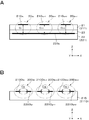
- FIG. 1 is a schematic cross-sectional view illustrating a configuration example of an input device according to the first embodiment of the present technology.
- FIG. 2 is an exploded perspective view illustrating a configuration example of the input device according to the first embodiment of the present technology.
- FIG. 3 is a schematic cross-sectional view illustrating a configuration example of a main part of the input device according to the first embodiment of the present technology.
- FIG. 4 is a block diagram illustrating a configuration example of an electronic device using the input device according to the first embodiment of the present technology.
- FIG. 5A is a schematic cross-sectional view illustrating a configuration example of a conductor layer according to the input device according to the first embodiment of the present technology.
- FIG. 5B is a schematic cross-sectional view showing a modification of the conductor layer.
- FIG. 5C is a schematic cross-sectional view showing a modification of the conductor layer.
- FIG. 5D is a schematic cross-sectional view showing a modification of the conductor layer.
- FIG. 5E is a schematic cross-sectional view showing a modification of the conductor layer.
- FIG. 6A is a schematic cross-sectional view for describing a configuration of a detection unit according to the input device according to the first embodiment of the present technology.
- FIG. 6B is a schematic cross-sectional view for explaining a configuration of a modified example of the detection unit.
- FIG. 6A is a schematic cross-sectional
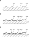
- FIG. 7A is a schematic cross-sectional view illustrating an example of a method of forming a first support according to the input device according to the first embodiment of the present technology.
- FIG. 7B is a schematic cross-sectional view showing an example of a method for forming the first support.
- FIG. 7C is a schematic cross-sectional view illustrating an example of a method for forming the first support.
- FIG. 8 is a schematic cross-sectional view illustrating an example of a method for forming the second support according to the input device according to the first embodiment of the present technology.
- FIG. 9A is a schematic cross-sectional view showing a modification of the method for forming the first or second support.
- FIG. 9B is a schematic cross-sectional view showing a modification of the method for forming the first or second support.
- FIG. 10A is a schematic diagram illustrating an arrangement example of the first and second electrode lines.
- FIG. 10B is a schematic diagram illustrating a configuration example of the first and second electrode lines.
- FIG. 10C is a schematic diagram for explaining a unit detection region.
- FIG. 11A is a schematic plan view illustrating an arrangement example of the first and second structures, the first electrode line (Y electrode), and the second electrode line (X electrode).
- FIG. 11B is a schematic plan view showing another arrangement example of the first and second structures, the first electrode line (Y electrode), and the second electrode line (X electrode).
- FIG. 12 is a schematic cross-sectional view showing the state of the force applied to the first and second structures when the point on the first surface of the input device is pressed downward in the Z-axis direction by the operator.
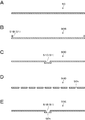
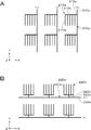
- FIG. 13A and FIG. 13B are diagrams for explaining advantages obtained by configuring the first and second electrodes with sub-electrodes.
- FIG. 14A and FIG. 14B are diagrams for explaining advantages obtained by configuring the first and second electrodes with sub-electrodes.
- FIG. 15 is a schematic cross-sectional view showing a main part of the input device when a point on the first structure of the first surface is operated by the operator, and the capacitance of each detection unit at that time. It is a figure which shows an example of variation
- FIG. 16 is a schematic cross-sectional view of the main part showing the aspect of the input device when a point on the first space portion of the first surface is operated by the operator, and the capacity of each detection unit at that time It is a figure which shows an example of variation
- FIG. 17 is a schematic cross-sectional view of an essential part showing an aspect of the input device when the first surface receives an operation with a stylus, and an example of a capacitance change amount of each detection unit at that time.
- FIG. 18 is a schematic cross-sectional view of an essential part showing an aspect of the input device when the first surface receives an operation with a finger, and a diagram showing an example of a capacitance change amount of each detection unit at that time.
- FIG. 17 is a schematic cross-sectional view of an essential part showing an aspect of the input device when the first surface receives an operation with a stylus, and an example of a capacitance change amount of each detection unit at that time.
- FIG. 18 is a
- FIG. 19A is a diagram illustrating an ideal capacity change rate distribution.
- FIG. 19B is a diagram showing an actual capacity change rate distribution.
- FIG. 20A is a schematic cross-sectional view illustrating an example of mounting the input device according to the first embodiment of the present technology on an electronic device.
- FIG. 20B is a schematic cross-sectional view illustrating a first modification example of mounting the input device according to the first embodiment of the present technology on an electronic device.
- FIG. 20C is a schematic cross-sectional view showing a second modification of the example of mounting the input device according to the first embodiment of the present technology on the electronic device.
- FIG. 21A is a plan view showing a modification of the first electrode line.
- FIG. 21B is a plan view showing a modification of the second electrode line.
- FIG. 22A to 22P are schematic views showing examples of the shape of the unit electrode body.
- FIG. 23 is a schematic cross-sectional view showing a modified example of the input device according to the first embodiment of the present technology.
- FIG. 24 is a schematic cross-sectional view illustrating a configuration example of the input device according to the second embodiment of the present technology.
- 25A and 25B are schematic cross-sectional views for explaining the cause of the occurrence of two split peaks in the capacity change rate distribution.
- 26A and 26B are schematic cross-sectional views for explaining the reason why the accuracy of coordinate calculation can be improved by including two or more first structures in the unit detection region.
- FIG. 27A is a plan view showing a first example of a symmetrical arrangement.
- FIG. 27A is a plan view showing a first example of a symmetrical arrangement.
- FIG. 27B is a plan view showing a second example of a symmetrical arrangement.
- FIG. 28A is a plan view showing a third example of a symmetrical arrangement.
- FIG. 28B is a plan view showing a fourth example of a symmetrical arrangement.
- FIG. 29A is a plan view showing a fifth example of a symmetrical arrangement.
- FIG. 29B is a plan view showing a sixth example of the symmetrical arrangement.
- FIG. 30 is a schematic cross-sectional view illustrating a configuration example of the input device according to the fifth embodiment of the present technology.
- FIG. 31A is a schematic cross-sectional view illustrating a configuration example of an operation member according to an input device according to a fifth embodiment of the present technology.
- FIG. 31B is a schematic cross-sectional view showing a modified example of the operation member.
- FIG. 32 is a schematic cross-sectional view illustrating a configuration example of an electronic apparatus in which an input device according to the sixth embodiment of the present technology is incorporated.
- 33A and 33B are schematic diagrams showing the simulation conditions in Test Examples 1-1 to 1-7.
- FIG. 34A is a diagram showing the results of simulation in Test Examples 1-1-1 to 1-1-7.
- FIG. 34B is a diagram showing simulation results for Test Examples 1-2-1 to 1-2-7.
- FIG. 35A is a diagram illustrating simulation results of Test Examples 1-3-1 to 1-3-6.
- FIG. 35B is a diagram showing simulation results for Test Examples 1-4-1 to 1-4-6.
- FIG. 36A and 36B are schematic diagrams showing the simulation conditions in Test Examples 1-5-1 to 1-5-4.
- FIG. 37A is a diagram showing the results of simulation in Test Examples 1-5-1 to 1-5-4.
- FIG. 37B is a diagram showing simulation results for Test Examples 1-6-1 to 1-6-4.
- FIG. 38A is a schematic diagram showing simulation conditions in Test Example 2-1.
- FIG. 38B is a schematic diagram showing simulation conditions in Test Example 2-1.
- FIG. 39A is a schematic diagram showing simulation conditions in Test Example 2-1.
- FIG. 39B is a schematic diagram showing simulation conditions in Test Example 2-2.
- FIG. 40A is a diagram illustrating a simulation result of Test Example 2-1.
- FIG. 40B is a diagram showing simulation results for Test Examples 2-1 to 2-5.
- FIG. 41 is an enlarged view of a part of FIG. 40B.
- FIG. 42 is a diagram showing the results of simulation in Test Examples 2-1 to 2-5.
- FIG. 43 is a diagram showing the results of simulation in Test Examples 3-1 to 3-5.
- 44A and 44B are schematic cross-sectional views for explaining the reason why the accuracy of coordinate calculation can be improved by including two or more first structures in the unit detection region.
- FIG. 45A is a schematic cross-sectional view showing a modified example of the input device according to the first embodiment of the present technology.
- FIG. 45B is a schematic cross-sectional view of an essential part showing a mode of the input device when the first surface receives an operation with a finger.
- FIG. 46A is a schematic plan view illustrating an arrangement example of the first and second structures, the first electrode line (Y electrode), and the second electrode line (X electrode).
- FIG. 46B is a schematic plan view illustrating another arrangement example of the first and second structures, the first electrode line (Y electrode), and the second electrode line (X electrode).
- FIG. 47A is a plan view showing a first example of arrangement positions of a plurality of openings in the in-plane direction of the input device.
- FIG. 47B is a plan view showing a second example of the arrangement positions of the plurality of openings in the in-plane direction of the input device.
- FIG. 48 is a plan view illustrating an example in which a plurality of second structures are arranged in the top of the unit detection region and in the vicinity of the top.
- FIG. 49A is a schematic diagram illustrating a first example of ground connection of the input device.
- FIG. 49B is a schematic diagram illustrating a second example of ground connection of the input device.
- FIG. 50 is a schematic cross-sectional view showing a modified example of the input device according to the first embodiment of the present technology.
- FIG. 51A is a perspective view illustrating a shape example of an input device having a cylindrical shape.
- 51B is a cross-sectional view along the line AA in FIG. 51A.
- FIG. 52A is a perspective view showing a shape example of an input device having a curved surface shape.
- 52B is a cross-sectional view along the line AA in FIG. 51A.
- FIG. 53A is a cross-sectional view showing an example of the configuration of the input device according to the second embodiment of the present technology.
- FIG. 53B is a cross-sectional view illustrating a part of FIG. 53A in an enlarged manner.
- FIG. 54A is a plan view showing an example of the configuration of the Y electrode.
- FIG. 54B is a plan view showing an example of the configuration of the X electrode.
- FIG. 55A is a plan view showing an example of an arrangement of X electrodes and Y electrodes.
- 55B is a cross-sectional view along the line AA in FIG. 55A.
- FIG. 56A is a cross-sectional view illustrating a first example of the configuration of the input device according to the modified example of the second embodiment of the present technology.
- FIG. 56A is a cross-sectional view illustrating a first example of the configuration of the input device according to the modified example of the second embodiment of the present technology.
- FIG. 56B is a cross-sectional view showing a second example of the configuration of the input device according to the modified example of the second embodiment of the present technology.
- FIG. 57A is a plan view showing a first example of the configuration of the Y electrode.
- FIG. 57B is a plan view showing a first example of the configuration of the X electrode.
- FIG. 58A is a plan view showing a second example of the configuration of the Y electrode.
- FIG. 58B is a plan view showing a second example of the configuration of the X electrode.
- FIG. 59A is a cross-sectional view showing a first example of the configuration of the input device according to the third embodiment of the present technology.
- FIG. 60A is a cross-sectional view illustrating a first example of the configuration of the input device according to the first modification of the third embodiment of the present technology.
- FIG. 60B is a cross-sectional view illustrating a second example of the configuration of the input device according to the first modification of the third embodiment of the present technology.
- FIG. 61A is a plan view illustrating a first example of the configuration of the X and Y electrodes in the input device according to the second modification of the third embodiment of the present technology.
- FIG. 61B is a plan view illustrating a second example of the configuration of the X and Y electrodes in the input device according to the second modification of the third embodiment of the present technology.
- FIG. 62A is a plan view showing an arrangement example of the first electrode lines (Y electrodes).
- FIG. 62B is a plan view showing an arrangement example of the second electrode lines (X electrodes).
- FIG. 63A is a plan view showing an arrangement example of the first structures.
- FIG. 63B is a plan view showing an arrangement example of the second structures.
- FIG. 64 is a plan view showing the positional relationship between the first and second electrode lines and the first and second structures.
- FIG. 65 is a plan view showing an arrangement example of the first and second structures.
- the sensor device and the input device include, for example, a notebook personal computer, a touch panel display, a tablet computer, a mobile phone (for example, a smartphone), a digital camera, a digital video camera, an audio device (for example, a portable audio player), and a game device. It is suitable for application to electronic equipment such as.
- the conductor layer may be a conductive layer having electrical conductivity, for example, an inorganic conductive layer including an inorganic conductive material, an organic conductive layer including an organic conductive material, an inorganic conductive material, and an organic It is preferable to use an organic-inorganic conductive layer containing both conductive materials.
- the inorganic conductive material examples include metals and metal oxides.
- the metal is defined to include a semi-metal.
- metals include copper, silver, gold, platinum, palladium, nickel, tin, cobalt, rhodium, iridium, iron, ruthenium, osmium, manganese, molybdenum, tungsten, niobium, tantel, titanium, bismuth, antimony, lead, and the like. However, it is not limited to these.
- the metal oxide examples include indium tin oxide (ITO), zinc oxide, indium oxide, antimony-added tin oxide, fluorine-added tin oxide, aluminum-added zinc oxide, gallium-added zinc oxide, silicon-added zinc oxide, and zinc oxide- Examples thereof include, but are not limited to, a tin oxide system, an indium oxide-tin oxide system, and a zinc oxide-indium oxide-magnesium oxide system.
- ITO indium tin oxide
- zinc oxide indium oxide
- indium oxide antimony-added tin oxide
- fluorine-added tin oxide aluminum-added zinc oxide
- gallium-added zinc oxide gallium-added zinc oxide
- silicon-added zinc oxide silicon-added zinc oxide
- zinc oxide- Examples thereof include, but are not limited to, a tin oxide system, an indium oxide-tin oxide system, and a zinc oxide-indium oxide-magnesium oxide system.
- organic conductive materials include carbon materials and conductive polymers.
- the carbon material include, but are not limited to, carbon black, carbon fiber, fullerene, graphene, carbon nanotube, carbon microcoil, and nanohorn.
- the conductive polymer for example, substituted or unsubstituted polyaniline, polypyrrole, polythiophene, and one or two (co) polymers selected from these can be used, but are not limited thereto. is not.
- Embodiments of the present technology will be described in the following order. 1. First embodiment (example of input device) 2. Second embodiment (example of input device) 3. Third embodiment (example of input device) 4). Fourth Embodiment (Example of input device) 5. Fifth embodiment (example of input device) 6). Sixth Embodiment (Example of electronic device)
- FIG. 1 is a schematic cross-sectional view illustrating a configuration example of the input device 100 according to the first embodiment of the present technology
- FIG. 2 is an exploded perspective view illustrating a configuration example of the input device 100
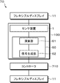
- FIG. FIG. 4 is a block diagram illustrating a configuration example of the electronic device 70 using the input device 100.
- FIG. Hereinafter, the configuration of the input device 100 of the present embodiment will be described.
- the X axis and Y axis indicate directions orthogonal to each other (in-plane direction of the input device 100)
- the Z axis indicates a direction orthogonal to the X axis and Y axis (thickness direction or vertical direction of the input device 100).
- the input device 100 includes a flexible display (display unit) 11 that receives a user's operation and a sensor device 1 that detects the user's operation.
- the input device 100 is configured as a flexible touch panel display, for example, and is incorporated in an electronic device 70 described later.
- the sensor device 1 and the flexible display 11 have a flat plate shape extending in a direction perpendicular to the Z axis.
- the flexible display 11 has a first surface 110 and a second surface 120 opposite to the first surface 110.
- the flexible display 11 has both a function as an input operation unit in the input device 100 and a function as a display unit. That is, the flexible display 11 causes the first surface 110 to function as an input operation surface and a display surface, and displays an image corresponding to an operation by the user from the first surface 110 facing upward in the Z-axis direction.
- On the first surface 110 for example, an image corresponding to a keyboard, a GUI (Graphical User Interface), and the like are displayed. Examples of the operator that performs an operation on the flexible display 11 include a finger f shown in FIG. 18 and a stylus s shown in FIG.
- the specific configuration of the flexible display 11 is not particularly limited.
- the flexible display 11 so-called electronic paper, an organic EL (electroluminescence) panel, an inorganic EL panel, a liquid crystal panel, or the like can be employed.
- the thickness of the flexible display 11 is not particularly limited, and is, for example, 0.1 mm to 1 mm.
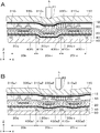
- the sensor device 1 includes a metal film (first conductor layer (conductive layer)) 12, a conductor layer (second conductor layer (conductive layer)) 50, an electrode substrate 20, a first support 30, A second support 40 is included.
- the sensor device 1 is disposed on the second surface 120 side of the flexible display 11.
- the metal film 12 has flexibility and is configured in a deformable sheet shape, for example.
- the conductor layer 50 is disposed to face the metal film 12.
- the electrode substrate 20 has flexibility, is arranged to face the plurality of first electrode lines 210 and the plurality of first electrode lines 210, and intersects the plurality of first electrode lines 210.
- the electrode substrate 20 has a plurality of second electrode lines 220 that intersect with the plurality of first electrode lines 210.
- the electrode substrate 20 is disposed so as to be deformable between the metal film 12 and the conductor layer 50, and can detect electrostatically a change in distance between the metal film 12 and the conductor layer 50.
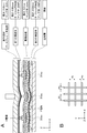
- the first support 30 is, for example, a first structure 310 that is formed between the plurality of first structures 310 that connect the metal film 12 and the electrode substrate 20 and the plurality of first structures 310. And a space 330.
- the metal film 12 and the electrode substrate 20 are separated from each other by the plurality of first structures 310.
- the second support body 40 includes, for example, a plurality of second structure bodies 410 that are respectively disposed between a plurality of adjacent first structure bodies 310 and connect between the conductor layer 50 and the electrode substrate 20. And a second space 430 formed between the second structures 410.
- the conductor layers 50 and the electrode substrate 20 are separated from each other by the plurality of second structures 410.
- the first space 330 and the second space 430 may be filled with a medium such as liquid or gel. Moreover, gas other than air may be filled.
- the sensor device 1 (input device 100) according to the present embodiment is provided between the metal film 12 and the electrode substrate 20 by the input operation on the first surface 110 of the flexible display 11, and between the conductor layer 50 and the electrode substrate 20.
- the input operation is detected by electrostatically detecting a change in the distance.
- the input operation is not limited to a conscious pressing (push) operation on the first surface 110 but may be a contact (touch) operation. That is, the input device 100 can detect even a minute pressing force (for example, about several tens of g) applied by a general touch operation, as will be described later.
- the touch operation is configured to be possible.
- the input device 100 includes a control unit 60, and the control unit 60 includes a calculation unit 61 and a signal generation unit 62.
- the calculation unit 61 detects an operation by the user based on the change in the capacitance of the detection unit 20s.
- the signal generator 62 generates an operation signal based on the detection result by the calculator 61.
- the electronic device 70 illustrated in FIG. 4 includes a controller 710 that performs processing based on an operation signal generated by the signal generation unit 62 of the input device 100.
- the operation signal processed by the controller 710 is output to the flexible display 11 as an image signal, for example.
- the flexible display 11 is connected to a drive circuit mounted on the controller 710 via a flexible wiring board 113 (see FIG. 2).
- the drive circuit may be mounted on the wiring board 113.
- the flexible display 11 is configured as a part of the operation member 10 of the input device 100 in the present embodiment. That is, the input device 100 includes the operation member 10, the electrode substrate 20, the first support body 30, the second support body 40, and the conductor layer 50. Hereinafter, each of these elements will be described.
- the operation member 10 has a laminated structure of the flexible display 11 including the first surface 110 and the second surface 120 and the metal film 12. That is, the operation member 10 has a first surface 110 that receives an operation by the user, and a second surface 120 that is formed with the metal film 12 and is opposite to the first surface 110, and has a deformable sheet shape. Composed.
- the metal film 12 is provided on the second surface 120 side facing the conductor layer 50.
- the metal film 12 is formed in a sheet shape that can be deformed following the deformation of the flexible display 11, and is formed of a metal foil such as Cu (copper), Al (aluminum), stainless steel (SUS), or a mesh material. . Moreover, it may be composed of a vapor-deposited film or a sputtered film of a conductor formed on a sheet-like substrate, or may be a coating film such as a conductive paste.
- the metal film 12 may function as a conductive layer, and may be an oxide conductor such as ITO (indium tin oxide) or an organic conductor such as carbon nanotube.
- the thickness of the metal film 12 is not particularly limited, and is, for example, several tens of nm to several tens of ⁇ m.
- the metal film 12 is connected to a ground potential, for example. Thereby, the metal film 12 exhibits a function as an electromagnetic shield layer when mounted on the electronic device 70. That is, for example, the invasion of electromagnetic waves from the flexible display 11, the invasion of electromagnetic waves from other electronic components mounted on the electronic device 70, and the leakage of electromagnetic waves from the input device 100 are suppressed, and the operation as the electronic device 70 is suppressed. It can contribute to stability. Moreover, in order to reinforce the function as such an electromagnetic shielding layer, the metal film 12 may be a plurality of layers.
- the metal film 12 is formed by attaching an adhesive layer 13 such as an adhesive resin film on which a metal foil is formed to the flexible display 11.
- an adhesive layer 13 such as an adhesive resin film on which a metal foil is formed
- it may be composed of a vapor deposition film or a sputtered film directly formed on the flexible display 11, or may be a coating film such as a conductive paste printed on the surface of the flexible display 11.
- a nonconductive film may be formed on the surface of the metal film 12 opposite to the flexible display 11.
- a scratch-resistant hard coat layer or a corrosion-resistant antioxidant film can be formed.
- the conductor layer 50 constitutes the lowermost part of the input device 100 and is disposed to face the metal film 12 in the Z-axis direction.
- the conductor layer 50 functions as a support plate of the input device 100, for example, and is configured to have higher bending rigidity than the operation member 10 and the electrode substrate 20, for example.
- the conductor layer 50 may be made of a conductor plate such as a metal plate containing Al alloy, Mg (magnesium) alloy or other metal material, or carbon fiber reinforced plastic.
- the conductor layer 50 may have a laminated structure in which a conductor film such as a plating film, a vapor deposition film, a sputtering film, or a metal foil is formed on an insulator layer such as a plastic material.
- the thickness of the conductor layer 50 is not specifically limited, For example, it is about 0.3 mm.
- FIGS. 5B, 5C, and 5E are schematic cross-sectional views showing examples of the configuration of the conductor layer 50.
- FIG. The conductor layer 50 is not limited to the example configured in a flat plate shape as shown in FIG. 5A, and may have a stepped portion 51 shown in FIGS. 5B, 5C, and 5E. Alternatively, the conductor layer 50 may be configured in a mesh shape.
- the conductor layer 50B shown in FIG. 5B has a stepped portion 51B formed by bending the peripheral portion upward in the Z-axis direction, and the conductor layers 50C and 50E shown in FIGS. 5C and 5E are both Step portions 51C and 51E are formed in the center and recessed downward.
- a stepped portion 51 can increase the bending rigidity of the conductor layer 50 in the Z-axis direction.
- one or a plurality of openings 50h are provided in the conductor layers 50D and 50E shown in FIGS. 5D and 5E.
- the openings 50h in the conductor layer 50 in this manner, it is possible to improve heat dissipation while maintaining rigidity, suppress problems of the input device 100, and improve reliability.
- the volume of the conductor layer 50 is reduced, and the weight of the input device 100 can be reduced.
- the opening 50h in the conductor layer 50 as described above air easily flows when the volume of the second space 430 changes due to deformation, and the response time of the electrode substrate 20 is shortened.
- the response time refers to the time from when the weight applied to the operation member 10 changes until the capacity of the sensor device 1 actually changes.
- the shape of the opening 50h examples include a polygonal shape such as a triangle and a quadrangle, a circular shape, an elliptical shape, an oval shape, an indefinite shape, and a slit shape, and these shapes may be used alone or in combination of two or more.
- the plurality of openings 50h are provided in the conductor layer 50, the plurality of openings 50h are arranged in a regular or irregular pattern. From the viewpoint of uniformity of sensor sensitivity, the regular pattern is preferable.
- the array may be a one-dimensional array or a two-dimensional array.
- the conductor layer 50 provided with the plurality of openings 50h may have a mesh shape or a stripe shape as a whole, or the plurality of openings 50h as a whole. It may constitute a geometric pattern.
- the opening 50h is provided in the conductor layer 50, it is preferable that the opening 50h is provided in a position or a region that does not face the second structure 410 or any of the second structures 410 constituting the group. That is, the opening 50h and the second structure 410 are provided so as to be shifted in the in-plane (XY plane) direction so as not to overlap with the Z-axis direction (that is, the thickness direction of the input device 100). Is preferred. This is because the electrode substrate 20 and the conductor layer 50 are stably connected by the second structure 410.
- the position of the opening 50h in the conductor layer 50 is preferably a position that does not face an intersecting region (detection unit 20s) of a plurality of electrode groups 21w and a plurality of electrode groups 22w described later. That is, it is preferable that the opening 50h and the detection unit 20s are provided so as to be shifted in the in-plane (XY plane) direction so as not to overlap with the Z-axis direction (that is, the thickness direction of the input device 100).
- the detection unit is compared with the case where the opening 50h of the conductor layer 50 is not disposed at a position facing the detection unit 20s. This is because the initial capacity and the capacity change rate of 20 s change, and the sensor sensitivity in the input device 100 becomes non-uniform.
- the arrangement positions of the openings 50h are all the same in each unit detection region 20r. However, the unit detection region 20r near the outermost periphery and the outermost periphery of the input device 100 is excluded. This is to prevent the sensor sensitivity from becoming uneven in the input device 100 as described above. Details of the unit detection area 20r will be described later. From the viewpoint of preventing the sensor sensitivity from becoming nonuniform, the opening 50h is preferably arranged symmetrically with respect to the center of the detection portion (intersection region) 20s. More specifically, the opening 50 h is preferably arranged symmetrically with respect to the center lines of the first and second electrode lines 210 and 220.
- FIG. 47A and 47B are plan views showing examples of arrangement positions of the plurality of openings 50h in the in-plane (XY plane) direction of the input device 100.
- FIG. FIG. 47A shows an example in which the opening 50h has an oval shape
- FIG. 47B shows an example in which the opening 50h has a circular shape.
- the plurality of openings 50h are disposed on the outer periphery (periphery) of the unit detection region 20r when viewed from the Z-axis direction (that is, the thickness direction of the input device 100), and the second structure 410 and the detection unit 20s.
- the opening 50h, the second structure 410, and the detection unit 20s are shifted in the in-plane (XY plane) direction so as not to overlap with each other in the Z-axis direction.
- the conductor layer 50 is connected to a ground potential, for example. Thereby, the conductor layer 50 exhibits a function as an electromagnetic shield layer when mounted on the electronic device 70. That is, for example, intrusion of electromagnetic waves from other electronic components mounted on the electronic device 70 and leakage of electromagnetic waves from the input device 100 can be suppressed, contributing to the stability of operation as the electronic device 70.
- the ground potential connection method of the metal film 12 and the conductor layer 50 is preferably as follows. .
- the metal film 12 and the conductor layer 50 it is preferable to connect the metal film 12 and the conductor layer 50 not only to the ground of the control unit 60 but also to the ground of the controller 710.
- the flexible display 11 is connected to the controller 710, and the shielding effect of the metal film 12 can be enhanced by connecting directly to the noise source. Further, the effect is high when the metal film 12 and the conductor layer 50 are coupled by many contacts.
- the ground connection of the conductor layer 50 is the control unit 60, a plurality of metal films 12 are arranged, and the metal film 12 provided closest to the flexible display 11 among these metal films 12. May be connected to the controller 710. Further, the ground connection of the metal film 12 provided closest to the electrode substrate 20 among the metal films 12 may be connected to both the control unit 60 and the controller 710.
- FIG. 57B shows an example in which two metal films 12 are provided.
- An adhesive layer 13 may be provided between the flexible display 11 and the metal film 12.
- the adhesive layer 13 is made of, for example, an insulating adhesive or pressure-sensitive adhesive tape.
- the adhesive for example, one or more selected from the group consisting of an acrylic adhesive, a silicone adhesive, a urethane adhesive, and the like can be used.
- pressure sensitive adhesion is defined as a kind of adhesion. According to this definition, the adhesive layer is regarded as a kind of adhesive layer.
- the entire surface of the flexible display 11 and the metal film 12 may be adhered by the adhesive layer 13. In this case, strong adhesion and uniform sensitivity can be obtained over the entire surface of the flexible display 11 and the metal film 12.
- the outer peripheral portion of the flexible display 11 and the metal film 12 may be bonded by the adhesive layer 13, and it is particularly preferable that both are bonded only at the upper portion of the first frame 320.
- the first frame member 320 has a stronger adhesive force than the first structure member 310, and when a force that causes the flexible display 11 to be pulled upward is applied, the first structure member 310 is destroyed. In addition, peeling of the metal film 12 and the first structure 310 can be suppressed, and peeling of the electrode substrate 20 and the first structure 310 can be suppressed.
- the flexible display 11 may be adhered by the adhesive layer 13.
- the adhesive layer 13 When wiring, FPC, a driver, etc. are attached to the outer peripheral part of the flexible display 11, damage to the flexible display 11 can be prevented, and the step on the outer peripheral part of the flexible display 11 can be bonded. It is possible to prevent an abnormality from occurring in the sensitivity of surrounding sensors.
- the step of the outer peripheral portion of the flexible display 11 is large or when warping is large, the flexible display 11 may be joined only inside the display area (effective area).
- the adhesive layer 13 for example, an adhesive layer continuously provided with a substantially uniform thickness between the flexible display 11 and the metal film 12, or a predetermined in-plane direction of the flexible display 11 and the metal film 12.
- An adhesive layer having the following pattern can be used.
- the pattern of the adhesive layer 13 may be either a one-dimensional pattern in which a predetermined adhesive pattern is repeated in one direction or a two-dimensional pattern in which a predetermined adhesive pattern is repeated in two directions.
- Specific examples of the pattern shape include a columnar shape, a stripe shape, and a lattice shape, but are not limited thereto.
- the thickness of the adhesive layer 13 is preferably thinner than the thickness of the metal film 12.
- the adhesive layer 13 is preferably higher definition than the first structure 310. That is, the size of the pattern of the adhesive layer 13 is preferably smaller than the size of the first structure 310. In this case, the size of the pattern of the adhesive layer 13 is preferably 1/10 or less of the size of the first structure 310.
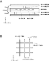
- the electrode substrate 20 is configured by a laminate of a first wiring substrate 21 having first electrode lines 210 and a second wiring substrate 22 having second electrode lines 220.
- the first wiring board 21 includes a first base material 211 (see FIG. 2) and a plurality of first electrode lines (Y electrodes) 210.
- the first substrate 211 is made of, for example, a flexible sheet material, specifically, an electrically insulating plastic sheet (film) such as PET, PEN, PC, PMMA, or polyimide.
- the thickness of the first base material 211 is not particularly limited, and is, for example, several tens of ⁇ m to several hundreds of ⁇ m.
- the plurality of first electrode wires 210 are integrally provided on one surface of the first base material 211.
- the plurality of first electrode lines 210 are arranged at a predetermined interval along the X-axis direction and are formed substantially linearly along the Y-axis direction.
- Each of the first electrode wires 210 is drawn out to the edge of the first base material 211 and connected to a different terminal.
- each of the first electrode wires 210 is electrically connected to the control unit 60 via these terminals.
- each of the plurality of first electrode lines 210 includes a plurality of electrode groups 21w (see FIG. 10B) arranged along the X-axis direction.
- the plurality of electrode lines constituting each electrode group 21w may be connected to a common terminal or may be divided into two or more different terminals.
- the second wiring board 22 includes a second base material 221 (see FIG. 2) and a plurality of second electrode wires (X electrodes) 220.
- the second substrate 221 is made of, for example, a flexible sheet material like the first substrate 211, and specifically, an electrically insulating plastic sheet (such as PET, PEN, PC, PMMA, polyimide) Film).
- the thickness of the second base material 221 is not particularly limited and is, for example, several tens of ⁇ m to several hundreds of ⁇ m.
- the second wiring board 22 is disposed to face the first wiring board 21.
- the plurality of second electrode lines 220 are configured in the same manner as the plurality of first electrode lines 210. That is, the plurality of second electrode lines 220 are arranged at a predetermined interval along the Y-axis direction and are formed substantially linearly along the X-axis direction. Each of the plurality of second electrode lines 220 includes a plurality of electrode groups 22w (see FIG. 10B) arranged along the Y-axis direction.
- Each of the second electrode wires 220 is drawn out to the edge of the second base material 221 and connected to a different terminal.
- the plurality of electrode lines constituting each electrode group 22w may be connected to a common terminal or may be divided and connected to two or more different terminals.
- each of the second electrode lines 210 is electrically connected to the control unit 60 via these terminals.
- the first and second electrode lines 210 and 220 may be formed of a conductive paste or the like by a printing method such as screen printing, gravure offset printing, or ink jet printing, or a metal foil or metal layer photolithography technique is used. It may be formed by a patterning method. Moreover, it can be set as the structure which has flexibility as the electrode substrate 20 whole because both the 1st and 2nd base materials 211 and 221 are comprised with the sheet
- the electrode substrate 20 has an adhesive layer 23 that joins the first wiring substrate 21 and the second wiring substrate 22 to each other.
- the adhesive layer 23 has electrical insulation and is made of, for example, an adhesive material such as a cured adhesive or an adhesive tape.
- the electrode substrate 20 is formed in the intersection region of the first electrode line 210 and the second electrode line 220, respectively, and each of the metal film (first conductor layer) 12 and the conductor layer (second conductor layer) 50.
- the plurality of detection units 20s whose capacity is variable according to the relative distance between them.
- a plurality of first structures 310 may constitute a group associated with each detection unit 20s.
- a plurality of second structures 410 may constitute a group associated with each detection unit 20s.
- the plurality of first and second structures 310 and 410 constituting each of these groups may be arranged symmetrically with respect to the center of the detection unit 20 (intersection region) s. More specifically, the first and second electrode lines 210 and 220 may be arranged symmetrically with respect to the center line.
- FIG. 6A is a schematic cross-sectional view for explaining the configuration of the detection unit 20s.
- the detection unit 20 s includes a first electrode line 210, a second electrode line 220 facing the first electrode line 210, and a dielectric layer provided between the first and second electrode lines 210 and 220. It is comprised with the capacitive element of a mutual capacitance system which has.
- FIGS. 6A and 6B description will be made assuming that each of the first and second electrode lines 210 and 220 is constituted by a single electrode line.
- FIG. 6A shows an example in which the first electrode lines 210 (210x i , 210x i + 1 , 210x i + 2 ) and the second electrode lines 220 (220y) are arranged facing each other in the Z-axis direction. Show.
- the first wiring board 21 and the second wiring board 22 are bonded to each other by the adhesive layer 23, and the first base material 211 and the adhesive layer 23 of the first wiring board 21 are Constitutes the dielectric layer.
- the detection units 20s i , 20s i + 1 , and 20s i are respectively provided in the intersecting regions where the first electrode lines 210x i , 210x i + 1 , 210x i + 2 and the second electrode line 220y are capacitively coupled. +2 is formed, and these capacitances C i , C i + 1 , C i + 2 are respectively connected to the metal film 12 and the conductor layer 50 and the first electrode lines 210x i , 210x i + 1 , 210x i +. 2 , configured to change according to capacitive coupling with the second electrode line 220y.
- the initial capacity of the detection unit 20s is, for example, the facing area between the first and second electrode lines 210 and 220, the facing distance between the first and second electrode lines 210 and 220, and the dielectric constant of the adhesive layer 23.
- FIG. 6B shows a modified example of the configuration of the detection unit 20s.
- the first electrode line 210D (210Dx i , 210Dx i + 1 , 210Dx i + 2 ) and the second electrode line 220D (220Dy i , 220Dy i). +1 , 220Dy i + 2 ) are arranged in the same plane on the first base material 211D and capacitively coupled in the XY plane.
- the first base material 211D constitutes a dielectric layer of the detection unit 20Ds (20Ds i , 20Ds i + 1 , 20Ds i + 2 ).
- the detection unit 20Ds i, 20Ds i + 1, 20Ds i + 2 of the capacitance Ca i, Ca i + 1, Ca i + 2 and the metal film 12 and the conductor layer 50 and each second It is variably configured according to capacitive coupling with the first and second electrode lines 210Dx and 220Dy. Further, the above configuration eliminates the need for the second base material and the adhesive layer, and can contribute to the thinning of the input device 100.
- each of the plurality of detection units 20s may be arranged to face the first structure 310 or a group formed by the first structure 310 in the Z-axis direction.
- the second structure body 410 or a group formed by the second structure body 410 may be disposed to face the Z-axis direction.
- the first wiring board 21 is stacked so as to be an upper layer than the second wiring board 22.
- the present invention is not limited to this, and the second wiring board 22 is formed from the first wiring board 21. May be laminated so as to be an upper layer.
- the controller 60 is electrically connected to the electrode substrate 20. More specifically, the control unit 60 is connected to each of the plurality of first and second electrode wires 210 and 220 via terminals.
- the control unit 60 configures a signal processing circuit capable of generating information (signal) related to an input operation on the first surface 110 based on the outputs of the plurality of detection units 20s.
- the control unit 60 acquires the capacitance change amount of each detection unit 20s while scanning each of the plurality of detection units 20s at a predetermined period, and generates information (signal) related to the input operation based on the capacitance change amount.
- the control unit 60 is typically composed of a computer having a CPU / MPU, a memory, and the like.
- the control unit 60 may be composed of a single chip component or a plurality of circuit components.
- the control unit 60 may be mounted on the input device 100 or may be mounted on the electronic device 70 in which the input device 100 is incorporated. In the former case, for example, it is mounted on a flexible wiring board connected to the electrode substrate 20. In the latter case, the electronic device 70 may be integrated with the controller 710.
- the control unit 60 includes the calculation unit 61 and the signal generation unit 62 as described above, and executes various functions according to a program stored in a storage unit (not shown).
- the computing unit 61 determines the operation position in the XY coordinate system on the first surface 110 based on electrical signals (input signals) output from the first and second electrode lines 210 and 220 of the electrode substrate 20.
- the signal generation unit 62 calculates and generates an operation signal based on the result. Thereby, an image based on an input operation on the first surface 110 can be displayed on the flexible display 11.
- the calculation unit 61 detects each of the detection units 20 s formed in the intersecting region of each Y electrode 210 and X electrode 220 based on the amount of change in capacitance obtained from each Y electrode 210 and X electrode 220. The amount of change in capacitance at is calculated.
- the XY coordinates of the operation position by the operator can be calculated based on the ratio of the change amount of the capacitance of each detection unit 20s.
- the calculation unit 61 can determine whether or not the first surface 110 is being operated. Specifically, for example, when the amount of change in the capacitance of the entire detection unit 20s or the amount of change in the capacitance of each detection unit 20s is equal to or greater than a predetermined threshold, the first surface 110 receives an operation. Can be determined. Further, by providing two or more threshold values, for example, it is possible to distinguish and determine a touch operation and a (conscious) push operation. Furthermore, it is also possible to calculate the pressing force based on the amount of change in capacitance of the detection unit 20s.
- the calculation unit 61 can output these calculation results to the signal generation unit 62.
- the signal generation unit 62 generates a predetermined operation signal based on the calculation result of the calculation unit 61.
- the operation signal is, for example, an image control signal for generating a display image to be output to the flexible display 11, an operation signal corresponding to a key of a keyboard image displayed at an operation position on the flexible display 11, or a GUI (Graphical User An operation signal related to an operation corresponding to (Interface) may be used.
- the input device 100 is configured to cause a change in the distance between the metal film 12 and the conductor layer 50 and the electrode substrate 20 (the detection unit 20s) by an operation on the first surface 110.
- Two supports 30, 40 are provided. Hereinafter, the first and second supports 30 and 40 will be described.
- the first support 30 is disposed between the operation member 10 and the electrode substrate 20.
- the first support 30 has a plurality of first structures 310, a first frame 320, and a first space 330.
- the 1st support body 30 is joined on the electrode substrate 20 via the contact bonding layer 35 (refer FIG. 3).
- the adhesive layer 35 may be an adhesive or may be composed of an adhesive material such as an adhesive tape.
- the first support 30 is formed at a predetermined position on the base material 31, the structural layer 32 provided on the surface (upper surface) of the base material 31, and the structural layer 32.
- a stacked structure of a plurality of bonded portions 341 is provided.
- the base material 31 is made of an electrically insulating plastic sheet such as PET, PEN, or PC.
- the thickness of the base material 31 is not particularly limited, and is, for example, several ⁇ m to several 100 ⁇ m.
- the structural layer 32 is made of an electrically insulating resin material such as UV resin, and forms a plurality of first convex portions 321, second convex portions 322, and concave portions 323 on the base material 31.
- Each of the first convex portions 321 has, for example, a columnar shape, a prismatic shape, a frustum shape, or the like protruding in the Z-axis direction, and is arranged on the substrate 31 at a predetermined interval.
- the second convex portion 322 is formed with a predetermined width so as to surround the periphery of the base material 31.
- the structural layer 32 is made of a material having a relatively high rigidity so that the electrode substrate 20 can be deformed by an input operation on the first surface 110, but the operation member 10 is at the time of the input operation. Further, it may be made of a deformable elastic material. That is, the elastic modulus of the structural layer 32 is not particularly limited, and can be appropriately selected as long as the desired operational feeling and detection sensitivity can be obtained.
- the concave portion 323 is configured by a flat surface formed between the first and second convex portions 321 and 322. That is, the space area on the recess 323 constitutes the first space 330. Further, an adhesion preventing layer 342 made of a UV resin having low adhesiveness may be formed on the recess 323 (not shown in FIG. 3). The shape of the adhesion preventing layer 342 is not particularly limited, and may be formed in an island shape, or may be formed as a flat film on the recess 323.
- each of the first structures 310 includes a stacked body of the first convex portion 321 and the joint portion 341 formed thereon, and each of the first frame bodies 320 includes the second convex portion 322. And a joined body 341 formed thereon.
- the thickness (height) of the first structure 310 and the first frame 320 is configured to be substantially the same, and is, for example, several ⁇ m to several hundred ⁇ m in the present embodiment.
- the height of the adhesion preventing layer 342 is not particularly limited as long as it is lower than the height of the first structure 310 and the first frame 320, and is lower than, for example, the first and second convex portions 321 and 322. Formed to be.
- the plurality of first structures 310 are arranged corresponding to the arrangement of the detection unit 20s or the unit detection region 20r, for example.
- the plurality of first structures 310 are disposed, for example, facing the plurality of detection units 20s or the unit detection regions 20r in the Z-axis direction.
- the first frame 320 is formed along the periphery of the electrode substrate 20 so as to surround the first support 30.
- the length in the short direction, that is, the width of the first frame 320 is not particularly limited as long as the strength of the entire first support 30 and the input device 100 can be sufficiently secured.
- the second support body 40 is disposed between the electrode substrate 20 and the conductor layer 50.
- the second support 40 includes a plurality of second structures 410, a second frame 420, and a second space 430.
- the second support 40 includes a second structure 410 and a second frame 420 that are directly formed on the conductor layer 50.
- the second structure body 410 and the second frame body 420 are made of, for example, an insulative resin material having adhesiveness, and also serve as a joint that joins between the conductor layer 50 and the electrode substrate 20.
- the thicknesses of the second structural body 410 and the second frame body 420 are not particularly limited, and are, for example, several ⁇ m to several hundred ⁇ m. Note that the thickness of the second structure body 410 is preferably smaller than the thickness of the first structure body 310. This is because the electrode substrate 20 is deformed until it bottoms on the conductor layer 50 as shown in FIG.
- the second structures 410 are respectively disposed between the adjacent first structures 310. That is, the second structures 410 are arranged corresponding to the arrangement of the detection units 20s, and are arranged between the adjacent detection units 20s in the present embodiment.
- the second frame 420 is formed so as to surround the periphery of the second support 40 along the periphery of the conductor layer 50.
- the width of the second frame body 420 is not particularly limited as long as the strength of the second support body 40 and the input device 100 as a whole can be sufficiently ensured.
- the elastic modulus of the second structural body 410 is not particularly limited as in the structural layer 32 constituting the first structural body 310. That is, it can be appropriately selected within a range in which a desired operation feeling and detection sensitivity can be obtained, and may be made of an elastic material that can be deformed together with the electrode substrate 20 during an input operation.
- the second space 430 is formed between the second structures 410 and constitutes a space region around the second structures 410 and the second frame 420.
- the second space 430 accommodates each detection unit 20s and each first structure 310 when viewed from the Z-axis direction.
- the first and second supports 30 and 40 configured as described above are formed as follows.
- (Method for forming first and second supports) 7A, 7 ⁇ / b> B, and 7 ⁇ / b> C are schematic cross-sectional views illustrating an example of a method for forming the first support 30.
- a UV resin is arranged on the base material 31a, and a predetermined pattern is formed on the resin.
- a structural layer 32a having a plurality of first and second convex portions 321a and 322a and a concave portion 323a is formed.
- the UV resin a solid sheet material or a liquid UV curable material may be used. Further, the pattern forming method is not particularly limited.
- the concave / convex pattern of the mold is transferred to the UV resin by a roll-shaped mold on which a predetermined concave / convex pattern is formed, and UV irradiation is performed from the substrate 31a side.
- a method of curing the UV resin by performing the above can be applied.
- it may be formed by general thermoforming (for example, press molding or injection molding) or by discharging a resin material with a dispenser or the like.
- a UV resin having low adhesiveness is applied in a predetermined pattern to the recess 323a by, for example, a screen printing method to form an adhesion preventing layer 342a.
- an adhesion preventing layer 342a may not be formed when the resin material forming the structural layer 32a has low adhesion.
- a joint 341a made of UV resin having high adhesiveness is formed on the convex portion 321a by, for example, a screen printing method.
- the first support 30 and the metal film 12 are bonded by the bonding portion 341a.
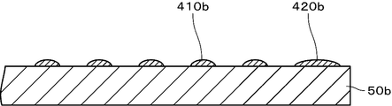
- FIG. 8 is a schematic cross-sectional view showing an example of a method for forming the second support 40.
- UV resin or the like having high adhesion is applied in a predetermined pattern directly on the conductor layer 50b by, for example, screen printing to form the second structure 410b and the second frame 420b.
- the number of processes can be greatly reduced and productivity can be increased.
- first support 30 may be formed by the method shown in FIG. 8, or the second support 40 may be formed by the method shown in FIG. Further, the first and second supports 30 and 40 can also be formed by the method shown in FIG. 9 below.
- FIG. 9A and FIG. 9B are schematic cross-sectional views showing a modification of the method for forming the first and second supports 30 and 40.
- description will be made with reference numerals corresponding to the first support 30.
- UV resin etc. are apply
- a joining portion 341c made of UV resin having high adhesiveness is formed on the first convex portion 311c and the second convex portion 312c, for example, by a screen printing method.
- the first structure 310 (second structure 410) configured by the first convex portion 311c and the joint portion 341c, and the first structure configured by the second convex portion 312c and the joint portion 341c.
- the frame body 320 (or the second frame body 420) can be formed.
- FIG. 10A is a schematic diagram illustrating an arrangement example of the first and second electrode lines 210 and 220.
- the first electrode line 210 is a Y electrode extending in the Y-axis direction and provided in a stripe shape.
- the second electrode line 220 is an X electrode extending in the X-axis direction and provided in a stripe shape.
- the first electrode line 210 and the second electrode line 220 are arranged so as to be orthogonal to each other.
- FIG. 10B is a schematic diagram illustrating a configuration example of the first and second electrode wires 210 and 220.
- the first electrode line 210 is constituted by an electrode group 21w composed of a group of a plurality of first sub-electrodes (first electrode elements) 21z.
- the first sub electrode 21z is, for example, a linear conductive member that extends in the Y-axis direction.
- the second electrode line 220 is composed of an electrode group 22w composed of a group of a plurality of second sub-electrodes (second electrode elements) 22z.
- the second sub electrode 22z is, for example, a linear conductive member that extends in the X-axis direction.
- the configuration of the first and second electrode lines 210 and 220 is not limited to this, and one of the first and second electrode lines 210 and 220 may be formed of a sub-electrode.
- a plurality of first electrode lines 210 are provided between the plurality of second electrode lines 220 and the metal film 12, and the first and second electrode lines 210 and 220 are A configuration in which the first electrode line 210 includes a plurality of sub-electrodes 21z may be employed.
- FIG. 10C is a schematic diagram for explaining the unit detection region 20r.
- a plurality of unit detection regions 20r are provided corresponding to the intersections of the first and second electrode lines 210 and 220.
- the unit detection region 20r includes a detection unit 20s provided at the intersection of the first and second electrode lines 210 and 220.
- the plurality of unit detection areas 20r are, for example, two-dimensionally filled and arranged in the X-axis direction (first direction) and the Y-axis direction (second direction).
- the unit detection region 20r has, for example, a square shape or a rectangular shape including a set of sides extending in the X axis direction and a set of sides extending in the Y axis direction.
- the filling arrangement of the plurality of unit detection regions 20r is a lattice-like (matrix-like) filling arrangement.
- the plurality of second structures 410 are arranged, for example, between the adjacent unit detection regions 20r. That is, the plurality of second structures 410 are arranged on the outer periphery (periphery) of the unit detection region 20r, for example. Further, the plurality of second structures 410 are arranged symmetrically with respect to the center of the unit detection region 20r, for example.
- the arrangement position of the second structure 410 includes the midpoint of each side forming the unit detection region 20r, and the top portions (corner portions) of the unit detection region 20r. And the vicinity of each apex (corner) of the unit detection region 20r, etc., and two or more of these arrangement positions may be combined.
- FIG. 10C shows an example in which the second structure 410 is arranged at each apex (corner) of the unit detection region 20r.
- the arrangement position of the second structure 410 is preferably the midpoint of each side forming the unit detection region 20r and each apex (corner portion) of the unit detection region 20r. More preferably, the position of the midpoint of each side forming the unit detection region 20r, more preferably the position of each apex (corner) of the unit detection region 20r. From the viewpoint of improving the adhesive force between the second structure 410 and the surfaces of the electrode substrate 20 and the conductor layer 50, the arrangement positions of the second structure 410 are the top portions (corner portions) of the unit detection region 20r. And the vicinity of each apex (corner) are preferred.
- the arrangement position of the second structure 410 is not limited to the above arrangement example, and the second structure 410 is arranged on the outer periphery (periphery) of the unit detection region 20r other than the above arrangement example. You may do it.
- FIG. 48 is a plan view showing an example in which a plurality of second structures 410 are arranged in the vicinity of each apex (corner) and each apex (corner) of the unit detection region 20r.
- the plurality of second structures 410 are arranged in a cross shape with the position ⁇ as an intersection.
- the position ⁇ is a position where each vertex of the four adjacent unit detection areas 20r is in contact.
- the arrangement intervals (arrangement intervals in the X-axis direction and the Y-axis direction) of the plurality of second structures 410 arranged in a cross shape are selected, for example, at equal intervals.
- FIG. 11A and FIG. 11B are schematic diagrams illustrating an arrangement example of the first and second structures 310 and 410, the first electrode line (Y electrode) 210, and the second electrode line (X electrode) 220. It is a top view. 11A and 11B show examples in which each Y electrode 210 and each X electrode 220 have electrode groups 21w and 22w, respectively. In addition, since each detection unit 20s is formed in the intersecting region of the Y electrode 210 and the X electrode 220 as described above, for example, six detection units 20s are arranged in FIGS. 11A and 11B. Note that the black circles illustrated in FIGS. 11A and 11B indicate the first structure 310, and the white circles indicate the second structure 410.
- the first electrode line (Y electrode) 210 and the first electrode line (X electrode) 220 overlap each other when viewed from the Z-axis direction (that is, the thickness direction of the input device 100). It is an area. Specifically, the formation region of the detection unit 20s in the X-axis direction configures the other end from the outer end surface of the first sub-electrode 21z that configures one end in the width direction of the first electrode line (Y electrode) 210. This is the range up to the outer end face of the first sub electrode 21z.
- the formation region of the detection unit 20 s in the Y-axis direction is the second that forms the other end from the outer end surface of the second sub-electrode 22 z that forms one end in the width direction of the second electrode line (X electrode) 220.
- This is a range up to the outer end face of the sub-electrode 22z.
- the outer end face of the first sub-electrode 21z means an end face far from the center of the detection unit 20s among both end faces of the first sub-electrode 21z in the x-axis direction.
- the outer end surface of the second sub-electrode 22z means an end surface far from the center of the detection unit 20s among both end surfaces of the second sub-electrode 22z in the y-axis direction.
- a unit detection area (unit sensor area) 20r is provided corresponding to the intersection of the Y electrode 210 and the X electrode 220.
- a detection unit 20s is provided in the unit detection region 20r.
- a plurality of second structures 410 are arranged on the outer periphery of the unit detection region 20r.
- the unit detection region 20r is a region obtained by equally dividing the main surface of the input device 100 so as to correspond to the intersection of the Y electrode 210 and the X electrode 220.
- the unit detection area 20r is defined as (A) or (B) below.
- the second structure 410 defines a unit. This is the position of each side (for example, the midpoint of each side) and / or the top (corner) of the detection region 20r.
- FIG. 11A shows an example in which the number of first structures 310 and second structures 410 is substantially the same. That is, the first structure 310 is disposed substantially at the center of the detection unit 20s.
- the pitch in the X-axis direction and the Y-axis direction of the first structure 310 is the same as the pitch in the X-axis direction and the Y-axis direction of the detection unit 20s, and is P1.
- the second structure 410 has the same pitch P1 as that of the first structure 310, and the first structure 310 and the detection unit 20s adjacent to each other in an oblique direction that forms approximately 45 ° with each of the X-axis and Y-axis directions. Are arranged at equal intervals.
- FIG. 11B shows an example in which the number of first structures 310 and second structures 410 is different. That is, the first structure 310 is arranged at a pitch P1 substantially on the center of the detection unit 20s, as in the example shown in FIG. 11A.
- the second structure body 410 is different in arrangement and number from FIG. 11A and is arranged at a pitch P2 that is 1 ⁇ 2 times the pitch P1 of the first structure 310, and is viewed from the Z-axis direction.
- the second structure 410 is disposed around the first structure 310 and the detection unit 20s.
- the metal film 12 and the conductor layer 50 with respect to the pressing force can be obtained so as to obtain a desired operation feeling and detection sensitivity.
- the amount of change in the distance between each and the detection unit 20s can be adjusted.
- the first and second supports 30 and 40 are (1) the first and second structures 310 and 410 and the first and second spaces 330 and 430. (2) The first structure 310 and the second structure 410 do not overlap each other when viewed from the Z-axis direction, and the first structure 310 is disposed on the second space 430. It has the feature that. Therefore, as shown below, the metal film 12 and the conductor layer 50 can be deformed even by a minute pressing force of about several tens of grams during operation.
- FIG. 12 is a schematic cross-section showing the state of the force applied to the first and second structures 310 and 410 when the point P on the first surface 110 is pressed downward in the Z-axis direction by the operating element h.
- FIG. The white arrow in the figure schematically shows the magnitude of the force downward in the Z-axis direction (hereinafter simply referred to as “downward”).
- FIG. 12 aspects such as the bending of the metal film 12 and the electrode substrate 20 and the elastic deformation of the first and second structures 310 and 410 are not shown.
- these input operations will be collectively described as “pressing”.
- the metal film 12 immediately below the point P bends downward.
- the first structures 310 i and 310 i + 1 adjacent to the first space 330 i receive the force F1, and elastically deform in the Z-axis direction to slightly reduce the thickness.
- the bending of the metal film 12, the first structure 310 i-1 adjacent to the structure 310 i, 310 i + 1 first, 310 i + 2 is also subjected to F1 less force F2.
- force is applied to the electrode substrate 20 by the forces F1 and F2, and the electrode substrate 20 bends downward about the region immediately below the first structures 310 i and 310 i + 1 .
- the second structure 410 i disposed between the first structures 310 i and 310 i + 1 receives the force F3 and is elastically deformed in the Z-axis direction to slightly reduce the thickness.
- the second structure 410 i-1 disposed between the first structures 310 i-1 and 310 i and the first structure 310 i + 1 and 310 i + 2 are disposed.
- the second structures 410 i + 1 also receive F4 smaller than F3.
- force can be transmitted in the thickness direction by the first and second structures 310 and 410, and the electrode substrate 20 can be easily deformed. Further, the metal film 12 and the electrode substrate 20 are bent, and the influence of the pressing force is exerted in the in-plane direction (direction parallel to the X-axis direction and the Y-axis direction). A force can also be exerted on the nearby first and second structures 310, 410.
- the metal film 12 and the electrode substrate 20 can be easily deformed by the first and second space portions 330 and 430. Furthermore, the first and second structures 310 and 410 formed of columns or the like can apply a high pressure to the electrode substrate 20 with respect to the pressing force of the operation element h, and the electrode substrate 20 can be flexed efficiently. I can do it.
- the first structure 310 since the first and second structures 310 and 410 are not overlapped when viewed from the Z-axis direction, the first structure 310 has a second space portion below it.
- the electrode substrate 20 can be easily bent toward the conductor layer 50 via 430.
- 13A and 13B schematically show a configuration of an input device in which the first and second electrode lines 210 and 220 are configured by the first and second sub-electrodes 21z and 22z.
- 14A and 14B schematically show the configuration of an input device in which the first and second electrode lines 210 and 220 are configured by a single plate-shaped first and second electrodes 21y and 22y.
- 13A and 14A show a state where the metal film 12 is not pressed
- FIGS. 13B and 14B show a state where the metal film 12 is pressed.
- the solid line La and the broken line Lb indicate electrode lines
- the broken line Lb of the solid line La and broken line Lb is the first and second sub-electrodes 21z, 22z
- this corresponds to a change in capacitance due to the first and second electrodes 21 y and 22 y approaching the conductor layer 50.
- illustration of members of the input device 100 is partially omitted for easy explanation.
- the capacitance changes by the amount that the metal film (GND) 12 and the conductor layer (GND) 50 absorb the electric field leaking from the ends of the first and second electrode lines 210 and 220. Is decided. That is, the capacity change becomes larger as the first and second electrode wires 210 and 220 have more ends.
- first and second electrode lines 210 and 220 are constituted by the first and second sub-electrodes 21z and 22z, the end portions of the first and second electrode lines 210 and 220 are increased, so that the capacitance change is large. Become.
- first and second electrode lines 210 and 220 are constituted by a single plate-shaped first and second sub-electrodes 21z and 22z, end portions of the first and second electrode lines 210 and 220 are formed. The coupling between the first and second electrode lines 210 and 220 is too strong, and the capacitance change is small.
- FIGS. 15 and 16 are schematic cross-sectional views showing the main part of the input device 100 when the first surface 110 is operated by the operator h, and the capacitance change amount of each detection unit 20s at that time. It is a figure which shows an example.
- the bar graphs shown along the X-axis in FIGS. 15 and 16 schematically show the amount of change from the reference value of the capacitance in each detection unit 20s.
- FIG. 15 shows a mode when the operator h presses the center of the unit detection region 20r, that is, the first structure 310 (310 i + 1 )
- FIG. 16 shows the unit detected by the operator h.
- a mode in which the middle of the region 20r and the adjacent unit detection region 20r, that is, the first space 330 (330 i + 1 ) is pressed is shown.
- the first structure 310 i + 1 immediately below the operation position receives the most force, and the first structure 310 i + 1 itself is elastically deformed and displaced downward. Due to the displacement, the detection unit 20s i + 1 immediately below the first structure 310 i + 1 is displaced downward. Thereby, the detection unit 20s i + 1 and the conductor layer 50 come close to or in contact with each other through the second space portion 430 i + 1 . That is, the detection unit 20s i + 1 obtains the change amount C i + 1 of the capacitance by changing the distance to the metal film 12 slightly and changing the distance to the conductor layer 50 greatly.
- the first structures 310 i and 310 i + 2 are also slightly displaced downward due to the influence of the bending of the metal film 12, and the amount of change in capacitance in the detection units 20s i and 20s i + 2 is as follows. , C i and C i +2 , respectively.
- C i + 1 is the largest, and C i and C i + 2 are substantially the same and smaller than C i + 1 . That is, as shown in FIG. 15, the capacitance changes C i , C i + 1 , and C i + 2 indicate mountain-shaped distributions having C i + 1 as the apex.
- the calculation unit 61 can calculate the center of gravity or the like based on the ratio of C i , C i + 1 , and C i + 2 , and can calculate the XY coordinates on the detection unit 20s i + 1 as the operation position. .
- the first structures 310 i + 1 and 310 i + 2 near the operation position are slightly elastically deformed and displaced downward due to the bending of the metal film 12. Due to the displacement, the electrode substrate 20 is bent, and the detection units 20s i + 1 and 20s i + 1 immediately below the first structures 310 i + 1 and 310 i + 2 are displaced downward. As a result, the detection units 20s i + 1 and 20s i + 2 and the conductor layer 50 come close to or in contact with each other through the second space portions 430 i + 1 and 430 i + 2 .
- each of the detection units 20s i + 1 and 20s i + 2 has a slight change in the distance from the metal film 12 and a relatively large change in the distance from the conductor layer 50.
- C i + 1 and C i + 2 are obtained.
- C i + 1 and C i + 2 are substantially the same.
- the calculating part 61 can calculate the XY coordinate between detection part 20s i + 1 and 20s i + 2 as an operation position.
- the capacitance of the detection unit 20s since both the thickness of the detection unit 20s and the metal film 12, and the detection unit 20s and the conductor layer 50 are variable depending on the pressing force, the capacitance of the detection unit 20s The amount of change can be made larger. As a result, it is possible to increase the detection sensitivity of the input operation.
- a finger and a stylus are often used as an operator.
- operation pressure a pressure against the pressing force
- the stylus has a small contact area.
- the amount of capacitive coupling with a sensor element is small and the detection sensitivity is low. According to the present embodiment, an input operation can be detected with high accuracy even when any of these operators is used.
- FIGS. 17 and 18 a description will be given with reference to FIGS. 17 and 18.
- FIG. 17 and 18 are schematic cross-sectional views showing the main part of the input device 100 when the first surface 110 is operated by a stylus or a finger, and an output signal output from the detection unit 20s at that time.
- FIG. 17 shows a case where the operation element is the stylus s
- FIG. 18 shows a case where the operation element is the finger f.
- the bar graphs shown along the X-axis in FIGS. 17 and 18 schematically show the amount of change from the reference value of the capacitance in each detection unit 20s, as in FIGS.
- the stylus s deforms the metal film 12 and exerts a pressing force on the first structure 310 i + 1 immediately below the operation position.
- the stylus s since the stylus s has a small contact area, a large operating pressure can be exerted on the metal film 12 and the first structure 310 i + 1 .
- the metal film 12 can be greatly deformed, and as a result, a large capacitance change can be caused as indicated by the capacitance change amount C i + 1 of the detection unit 20s i + 1. It becomes possible.
- the capacitance changes C i , C i + 1 , C i + 2 of the detection units 20s i , 20s i + 1 , 20s i + 2 are distributed in a mountain shape with C i + 1 as the vertex. It becomes.
- the input device 100 can detect the amount of change in capacitance based on the in-plane distribution of the operating pressure. This is because the input device 100 does not detect the amount of change in capacitance due to direct capacitive coupling with the operation element, but the amount of change in capacitance via the deformable metal film 12 and the electrode substrate 20. By detecting. Therefore, even with an operator such as the stylus s having a small contact area, the operation position and the pressing force can be detected with high accuracy.
- the input device 100 detects the amount of change in capacitance based on capacitive coupling between the metal film 12 and the conductor layer 50 and the detection unit 20s as described above, the finger f Even with an operator having a large contact area as described above, a sufficient change in capacitance can be caused.
- determining whether or not an operation has been performed for example, a value obtained by summing the amount of change in capacitance of all the detection units 20s i , 20s i + 1 , and 20s i + 2 in which changes in capacitance have occurred.
- the operation position and the like are detected using capacitive coupling between the operation element and the X and Y electrodes. That is, when a conductor is disposed between the operation element and the X and Y electrodes, it is difficult to detect an input operation due to capacitive coupling between the conductor and the X and Y electrodes. Further, in the configuration in which the thickness between the operation element and the X and Y electrodes is large, there is a problem that the amount of capacitive coupling between them becomes small and the detection sensitivity decreases. Under these circumstances, it is necessary to dispose the sensor device on the display surface of the display, and the display quality of the display deteriorates.
- the input device 100 (sensor device 1) according to the present embodiment uses capacitive coupling between the metal film 12 and the conductor layer 50 and the X and Y electrodes 220 and 210, between the operating element and the sensor device. Even if a conductor is disposed on the surface, there is no influence on the detection sensitivity. Further, it is only necessary that the metal film 12 can be deformed by the pressing force of the operation element, and there are few restrictions on the thickness between the operation element and the X and Y electrodes. Therefore, even when the sensor device 1 is arranged on the back surface of the flexible display 11, the operation position and the pressing force can be detected with high accuracy, and deterioration of display characteristics of the flexible display 11 can be suppressed.
- the thickness of the insulator dielectric material
- the detection sensitivity does not decrease. Therefore, it is possible to contribute to improvement of user convenience.
- FIG. 19A is a diagram illustrating an ideal capacity change rate distribution.
- C i and C i + 1 indicate the center positions of the unit detection areas 20r i and 20r i + 1 (detectors 20s i and 20s i + 1 ), respectively.
- L i, L i + 1, respectively, the unit detection area 20r with respect to the X-axis direction i, 20r i + 1 (detector 20s i, 20s i + 1) represents the rate of change in capacitance distribution.
- the capacitance change rate distribution is the ideal distribution shown in FIG. 19A.
- the distribution tends to be as shown in FIG. 19B. That is, the unit detection area 20r i, 20r i + 1 of the center position C i, the peak of the rate of change of capacity distribution C i + 1 rather than appear one its center position C i, a C i + 1 as the center There is a tendency for the peak to appear in two. The regions R i and R i + 1 between the two peaks split in this way cause a shift in coordinate calculation.
- FIG. 44A when the position P1 corresponding to the center of the unit detection region 20ri + 1 in the first surface 110 is pressed by the operator h, the metal film 12 and the electrode substrate 20 have substantially the same shape. Transforms into Thereby, even after pressing, the distance between the metal film 12 and the electrode substrate 20 is kept substantially constant.
- FIG. 44B when the position P2 between the unit detection areas 20r i + 1 and 20r i + 2 in the first surface 110 is pressed by the operating element h, the vicinity of the pressed position P2 Only the metal film 12 is greatly deformed.
- FIG. 25A and FIG. 25B by adopting a configuration in which the first sub-electrode 21z and the second sub-electrode 22z are gathered near the center of the unit detection region 20r, The reason why the occurrence of the peak can be suppressed will be described.
- FIG. 25A when the position P1 corresponding to the center of the unit detection region 20ri + 1 in the first surface 110 is pressed by the operator h, the metal film 12 and the electrode substrate 20 have substantially the same shape. Transforms into Thereby, even after pressing, the distance between the metal film 12 and the electrode substrate 20 is kept substantially constant.
- FIG. 25A when the position P1 corresponding to the center of the unit detection region 20ri + 1 in the first surface 110 is pressed by the operator h, the metal film 12 and the electrode substrate 20 have substantially the same shape. Transforms into Thereby, even after pressing, the distance between the metal film 12 and the electrode substrate 20 is kept substantially constant.
- FIG. 25A when the position P1 corresponding to the center of the
- the density of the electrode intersections of the first and second sub-electrodes 21z and 22z is the peripheral part (detection part) of the intersection region of the first and second electrode lines 210 and 220. It is preferable that the central portion is higher than the peripheral portion of 20s. Thereby, compared with the case where the density of a sub electrode intersection is made constant, the magnitude
- the density of the intersections of the sub-electrodes is preferably higher in the position or region facing the first structure 310 or the group of the first structure 310 than the position or region facing the second structure 410. .
- the position or region facing the group of the first structures 310 means “the circumference (periphery) of the polygon having the plurality of first structures 310 constituting the group as vertices. It means “opposing position or region”. Examples of the polygonal shape include a square and a rectangle, but are not limited thereto.
- the sub electrode intersection is preferably not provided at a position or a region facing the second structure 410.
- the magnitude of the two peaks generated in the capacity change rate distribution can be reduced as compared with the case where the sub-electrode intersection is provided at a position or region facing the second structure 410.
- the sub-electrode intersection is preferably provided in a region facing the first structure 310 or the group of the first structures 310, or inside the region.
- the load sensitivity can be improved because the first sub-electrode 21z and the second sub-electrode 22z are gathered near the center of the unit detection region 20r.
- the first sub-electrode 21z and the second sub-electrode 22z are gathered in the vicinity of the center of the unit detection region 20r. The reason why it can be improved will be described.
- FIG. 44A shows an example of the input device 100 that includes one first structure 310 in the unit detection region 20r, and the density of the sub electrode intersections is substantially constant in the unit detection region 20r. .
- the capacity change rate was calculated by the following formula.
- (Capacity change rate) [%] [(Initial capacity C 0 ) ⁇ (Capacity after change C 1 )] / (Initial capacity C 0 )
- “initial capacity C 0 ” and “changed capacity C 1 ” specifically show the following contents.
- Initial capacitance C 0 Capacitance of the input device when no weight is applied to the surface of the operating member
- Changed capacitance C 1 Capacitance of the input device after applying a weight to the surface of the operating member
- the unit detection region 20r includes one first structure 310, and the first sub-electrode 21z and the second sub-electrode 22z are gathered near the center of the unit detection region 20r.
- An example of the input device 100 is shown. In the input device 100 shown in this example, when the position P1 corresponding to the center of the unit detection region 20ri + 1 in the first surface 110 is pressed by the operator h, as shown in FIG. Only the electrode substrate 20 directly under the structure 310 is locally deformed toward the conductor layer 50.
- the capacitance change at the intersection of the sub-electrodes immediately below the first structure 310 is very large, and the intersections of the sub-electrodes are densely located immediately below the first structure 310, so that the entire detection unit 20s
- the capacitance change rate is larger than when the density of the sub-electrode intersections is substantially constant in the unit detection region 20r.
- the amount of change in capacity when the position P2 corresponding to the center of the unit detection region 20ri + 1 is pressed by the operation element h increases.
- the maximum capacity change rate and sensitivity are higher than when the density of the intersection of the sub-electrodes is constant.
- the sensitivity load sensitivity
- the maximum capacity change rate and sensitivity can be further improved by not providing the sub-electrode intersection at the position facing the second structure.
- the sub-electrode intersection should not be provided at the position facing the second structure.
- the maximum capacity change rate and the sensitivity can be further improved by providing the sub electrode intersections within the range of 1/3 of the width Lx, Ly of the unit detection region. Can do.
- FIG. 26A two or more first structures 310 are included in the unit detection region 20r, and the first sub-electrode 21z and the second sub-electrode 22z are included in a plurality of first structure groups.
- An example of an input device 100 is shown that is confronted or gathered inside the region.
- the electrode substrate 20 in a wide range surrounded by the first structure 310 near the center of the unit detection region 20ri + 1 is deformed toward the conductor layer 50.
- the capacitance change in a wider range surrounded by the first structure 310 in the vicinity of the center of the unit detection region 20ri + 1 is very large, and the intersections of the sub electrodes are dense within this range.
- the capacity change rate of the entire portion 20s the capacity change rate is larger than when the density of the sub-electrode intersections is substantially constant in the unit detection region 20r.
- the amount of change in capacity when the position P2 corresponding to the center of the unit detection region 20ri + 1 is pressed by the operation element h increases. Further, compared to the case of FIG.
- the electrode substrate 20 in a wider range is deformed, a region where the density of the sub-electrode intersections is large can be taken in a wide range, so that the first sub-electrode 21z and the second sub-electrode 22z The number of can be increased.
- the initial capacity C 0 can be increased while increasing the capacity change rate, and the S / N is improved.
- FIG. 20A, 20B, and 20C are diagrams illustrating examples of mounting the input device 100 according to the present embodiment on the electronic device 70.
- FIG. An electronic device 70a according to FIG. 20A includes a housing 720a including an opening 721a in which the input device 100 is disposed.
- a support portion 722a is formed in the opening 721a and supports the peripheral portion of the conductor layer 50 through a joint portion 723a such as an adhesive tape.
- the joining method of the conductor layer 50 and the support part 722a is not limited to the above, For example, you may fix with a screw
- the input device 100 can maintain a stable strength even during mounting.
- the electronic device 70b according to FIG. 20B has substantially the same configuration as the electronic device 70a, and includes a housing 720b including an opening 721a and a support 722a. The difference is that it has at least one auxiliary support portion 724 b that supports the back surface of the conductor layer 50.
- the auxiliary support part 724b supports the input device 100 from the back surface of the conductor layer 50 to the periphery of the detection unit 20s or at a position facing the first structure 310 from the back surface of the conductor layer 50. With this configuration, the input device 100 can be supported more stably.
- the auxiliary support part 724b may be joined to the conductor layer 50 with an adhesive tape or the like, or may not be joined.
- An electronic device 70b according to FIG. 20C has substantially the same configuration as the electronic device 70b and includes a housing 720b including an opening 721a and a support 722a. The difference is that an auxiliary support portion 724 b that supports the back surface of the conductor layer 50 is disposed under the second structure 410.
- the auxiliary support part 724b may be joined to the conductor layer 50 with an adhesive tape or the like, or may not be joined.
- the input device 100 receives a load from the auxiliary support portion 724b, and the load is mainly transmitted to the second structure 410 immediately above, and the second structure 410 deforms the electrode substrate.
- the density of the sub-electrode intersection of the portion deformed by the second structure 410 is It is small and the amount of capacitance change is small.
- the auxiliary support portion 724b exists near the center of the unit detection region 20ri + 1 as shown in FIG. 20B, the conductor layer 50 is deformed by receiving a load from the auxiliary support portion 724b, and the deformation is detected by unit detection. Detection is performed at a sub-electrode intersection near the center of the region 20r. Therefore, the input device 100 can be more stably supported by the configuration in which the auxiliary support portion 724 b that supports the back surface of the conductor layer 50 is disposed under the second structure 410.
- the input device 100 detects the amount of change in capacitance based on capacitive coupling between the metal film 12 and the conductor layer 50 and the detection unit 20s as described above, the finger f Even with an operator having a large contact area as described above, a sufficient change in capacitance can be caused.
- determining whether or not an operation has been performed for example, a value obtained by summing the amount of change in capacitance of all the detection units 20s i , 20s i + 1 , and 20s i + 2 in which changes in capacitance have occurred.
- the initial capacity and the capacity change rate can be increased.
- the signal-to-noise ratio of the input device 100 can be improved.
- the capacity change rate in this way, it is possible to improve the operation sensitivity of the input device.
- the operation position and the like are detected using capacitive coupling between the operation element and the X and Y electrodes. That is, when a conductor is disposed between the operation element and the X and Y electrodes, it is difficult to detect an input operation due to capacitive coupling between the conductor and the X and Y electrodes. Further, in the configuration in which the thickness between the operation element and the X and Y electrodes is large, there is a problem that the amount of capacitive coupling between them becomes small and the detection sensitivity decreases. Under these circumstances, it is necessary to dispose the sensor device on the display surface of the display, and the display quality of the display deteriorates.
- the input device 100 uses capacitive coupling between the metal film 12 and the conductor layer 50 and the X and Y electrodes 210 and 220, and therefore, between the operator and the sensor device. Even if a conductor is disposed on the surface, there is no influence on the detection sensitivity. Further, it is only necessary that the metal film 12 can be deformed by the pressing force of the operation element, and there are few restrictions on the thickness between the operation element and the X and Y electrodes. Therefore, even when the sensor device 1 is arranged on the back surface of the flexible display 11, the operation position and the pressing force can be detected with high accuracy, and deterioration of display characteristics of the flexible display 11 can be suppressed.
- FIG. 21A is a plan view showing a modification of the first electrode wire 210.
- the first electrode line 210 includes a plurality of unit electrode bodies 210m and a plurality of connecting portions 210n that connect the plurality of unit electrode bodies 210m to each other.
- the unit electrode body 210m is composed of an electrode group composed of a group of a plurality of sub-electrodes (electrode elements), and these sub-electrodes have a regular or irregular pattern.
- the unit electrode body 210m is composed of an assembly of a plurality of linear electrode patterns extending radially from the center.
- the connecting portion 210n extends in the Y-axis direction and connects adjacent unit electrode bodies 210m.
- FIG. 21B is a plan view showing a modification of the second electrode wire 220.
- the second electrode line 220 includes a plurality of unit electrode bodies 220m and a plurality of connecting portions 220n that connect the plurality of unit electrode bodies 220m to each other.
- the unit electrode body 220m is composed of an electrode group composed of a group of a plurality of sub-electrodes (electrode elements), and these sub-electrodes have a regular or irregular pattern.
- the unit electrode body 220m is composed of an assembly of a plurality of linear electrode patterns extending radially from the center.
- the connecting portion 220n extends in the X-axis direction and connects adjacent unit electrode bodies 220m.
- the first and second electrode lines 210 and 220 are arranged so as to intersect each other so that the unit electrode body 210m and the unit electrode body 220m overlap each other when viewed from the Z-axis direction.
- 22 (A) to 22 (P) are schematic views showing examples of shapes of the unit electrode bodies 210m and 220m.
- 22A to 22P show the shapes at the intersections of the first and second electrode lines 210 and 220, and the shapes of the other portions are not particularly limited. For example, it may be linear.
- the combination of the shapes of the unit electrode bodies 210m and 220m of the first and second electrode wires 210 and 220 is two sets of the same type in FIG. 10 (B) or FIG. 22 (A) to FIG. 22 (P). However, two different sets may be used.
- FIG. 22A corresponds to the unit electrode bodies 210m and 220m in FIGS. 21A and 21B.
- FIG. 22B shows an example in which one of the radial line electrodes shown in the example of FIG. 21A is formed thicker than the other line electrodes. Thereby, the electrostatic capacitance change amount on a thick line electrode can be made higher than on other line electrodes.
- FIGS. 22C and 22D show an example in which an annular linear electrode is disposed substantially at the center, and the radial linear electrodes are formed therefrom. Thereby, the concentration of the linear electrodes in the central portion can be suppressed, and the occurrence of the sensitivity reduction region can be prevented.
- 22 (E) to 22 (H) show examples in which an aggregate is formed by combining a plurality of linear electrodes formed in an annular shape or a rectangular annular shape. As a result, the density of the electrodes can be adjusted, and the formation of the sensitivity reduction region can be suppressed.
- 22 (I) to 22 (L) each show an example in which an aggregate is formed by combining a plurality of linear electrodes arranged in the X-axis direction or the Y-axis direction. By adjusting the shape, length, pitch, and the like of the linear electrode, a desired electrode density can be obtained.
- 22 (M) to 22 (P) are examples in which the line electrodes are arranged asymmetrically in the X-axis direction or the Y-axis direction.
- FIG. 23 is a schematic cross-sectional view illustrating a modified example of the input device 100 according to the first embodiment of the present technology.
- the plurality of second supports 40 are not provided between the electrode substrate 20 and the conductor layer 50, and the electrode substrate 20 and the conductor layer 50 are provided adjacent to each other. Other points are the same as those in the first embodiment.
- the first structure 310 is disposed at the center of the detection unit 20s, but may be disposed between adjacent detection units 20s.
- FIG. 50 is a schematic cross-sectional view showing a modified example of the input device 100 according to the first embodiment of the present technology.
- the plurality of first supports 30 are not provided between the electrode substrate 20 and the metal film 12, and the electrode substrate 20 and the metal film 12 are provided adjacent to each other. Other points are the same as those in the first embodiment.
- the second structure 410 is disposed between the adjacent detection units 20s, but may be disposed at the center of the detection unit 20s.
- Modification 4 Arrangement position between the layers of the first and second structures 310 and 410 in the first embodiment (position between the metal film 12 and the electrode substrate 20 and between the conductor layer 50 and the electrode substrate 20) May be interchanged.
- the input device 100 having such a switched configuration will be described.
- FIG. 45A is a schematic cross-sectional view showing a modified example of the input device 100 according to the first embodiment of the present technology.
- the first structure 310a is obtained by providing the second structure 410 in the first embodiment between the metal film 12 and the electrode substrate 20, and other points (that is, the arrangement position in the in-plane direction).
- the second structure 410 is the same as the second structure 410 in the first embodiment.
- the second structure 410a is obtained by providing the first structure 310 in the first embodiment between the conductor layer 50 and the electrode substrate 20, and other points (that is, arrangement positions in the in-plane direction).
- Configuration, material, formation method, and the like are the same as those of the first structure 310 in the first embodiment.
- the detection unit 20s may be arranged to face the second structure 410a or a group formed by the second structure 410 in the Z-axis direction.
- FIG. 45B is a schematic cross-sectional view of an essential part showing an aspect of the input device 100 when the first surface 110 receives an operation with the finger f.
- the operation member 10 metal film 12
- the operation member 10 metal film 12
- the operation member 10 metal film 12 in the immediate vicinity and the vicinity thereof is deformed toward the electrode substrate 20, Proximity or contact with 20.
- the variations of the operating member 10 the first structure 310a i, unit detection area 20r i, 20r i + 1 and between the unit detection area 20r i + 1 of the electrode substrate 20 through the 310a i + 1, A force is applied to a portion corresponding to 20 r i + 2 , and the portion is deformed toward the conductor layer 50 and comes close to the conductor layer 50.
- the density of the intersections of the sub electrodes is preferably higher in the position or region facing the second structure 410 or the group of the second structure 410 than in the position or region facing the first structure 310. .
- the position or region facing the group of the second structure 410 means “the circumference (periphery) of a polygon having a plurality of second structures 410 constituting the group as vertices. It means “opposing position or region”. Examples of the polygonal shape include a square and a rectangle, but are not limited thereto.
- the sub electrode intersection is not provided at a position or a region facing the first structure 310. Thereby, the magnitude of the two peaks generated in the capacitance change rate distribution can be reduced as compared with the case where the sub-electrode intersection is provided at a position or region facing the first structure 310.
- the sub-electrode intersection is preferably provided in a region facing the second structure 410 or the group of the second structures 410 or inside the region.
- the shape of the input device 100 is not limited to this.
- the input device 100 may have a cylindrical shape, a curved surface shape, a belt shape, an indefinite shape, or the like.
- the curved surface include a curved surface having a cross section such as an arc, an elliptical arc, or a parabola.
- the entire input device 100 may have rigidity or may have flexibility. When the entire input device 100 has flexibility, the input device 100 may be a wearable device.
- FIG. 51A is a perspective view showing a shape example of the input device 100 having a cylindrical shape.
- 51B is a cross-sectional view along the line AA in FIG. 51A.
- the thickness of the input device 100 is shown larger than that of FIG. 51A.
- the flexible display 11 is provided on the outer peripheral surface side of the input device 100, and the conductor layer 50 is provided on the inner peripheral surface side. Therefore, the outer peripheral surface side of the input device 100 functions as an input operation surface and a display surface.
- the input device 100 may be used by fitting it to a support body 100j having a cylindrical shape or a human body such as a wrist. Further, the belt-like input device 100 may be used by being wound around a support body 100j having a cylindrical shape or a human body such as a wrist.
- FIG. 52A is a perspective view showing a shape example of the input device 100 having a curved surface shape.
- FIG. 52B is a cross-sectional view along the line AA in FIG. 52A.
- the thickness of the input device 100 is shown larger than that of FIG. 52A.
- FIG. 52B shows an example where the convex curved surface side functions as an input operation surface and a display surface by providing the flexible display 11 on the convex curved surface side and providing the conductor layer 50 on the concave curved surface side.
- the concave curved surface side functions as an input operation surface and a display surface. Also good.
- the input device 100 may be used by being fitted to a support body 100k having a convex curved surface or a human body such as a wrist. Further, the belt-like input device 100 may be mounted and used so as to follow a human body such as a support 100k having a convex curved surface or a wrist.
- FIG. 24 is a schematic cross-sectional view illustrating a configuration example of the input device according to the second embodiment of the present technology.
- the input device 100C according to the second embodiment is different from the input device 100 according to the first embodiment in that two or more first structures 310 are included in the unit detection region 20r.
- the first structure 310 when the first structure 310 is arranged on the outer periphery of the unit detection region 20r, one first structure existing inside the unit detection region 20r to which attention is focused with the outer periphery as a boundary. It is defined that a part of the body 310 is counted as the number of the first structures 310. Specifically, for example, when the first structures 310 are arranged so as to be divided into two on the side constituting the unit detection region 20r, the number of the first structures 310 is “ 1/2 ". Further, when the first structures 310 are arranged at the top (corner) of the square or rectangular unit detection region 20r, the number of the first structures 310 is “1/4”. Define.
- the input device 100 since the input device 100 includes two or more first structures in the unit detection region, the occurrence of two peaks in the capacity change rate distribution (see FIG. 19B) is suppressed, and coordinate calculation is performed. Accuracy can be improved.
- FIG. 44A when the position P1 corresponding to the center of the unit detection region 20ri + 1 in the first surface 110 is pressed by the operator h, the metal film 12 and the electrode substrate 20 have substantially the same shape. Transforms into Thereby, even after pressing, the distance between the metal film 12 and the electrode substrate 20 is kept substantially constant.
- FIG. 44B when the position P2 between the unit detection areas 20r i + 1 and 20r i + 2 in the first surface 110 is pressed by the operating element h, the vicinity of the pressed position P2 Only the metal film 12 is greatly deformed.
- FIGS. 26A and 26B the reason why the occurrence of two peaks can be suppressed by including two or more first structures 310 in the unit detection region 20r will be described with reference to FIGS. 26A and 26B.
- FIG. 26A when the position P1 corresponding to the center of the unit detection region 20ri + 1 in the first surface 110 is pressed by the operator h, the metal film 12 and the electrode substrate 20 have substantially the same shape. Transforms into Thereby, even after pressing, the distance between the metal film 12 and the electrode substrate 20 is kept substantially constant.
- FIG. 26A when the position P1 corresponding to the center of the unit detection region 20ri + 1 in the first surface 110 is pressed by the operator h, the metal film 12 and the electrode substrate 20 have substantially the same shape. Transforms into Thereby, even after pressing, the distance between the metal film 12 and the electrode substrate 20 is kept substantially constant.
- FIG. 26A when the position P1 corresponding to the center of the unit detection region 20ri + 1 in the first surface 110 is pressed
- Example of arrangement of first and second structures 46A and 46B are schematic diagrams showing examples of arrangement of the first and second structures 310 and 410, the first electrode line (Y electrode) 210, and the second electrode line (X electrode) 220. It is a top view. Two or more first structures 310 are included in the unit detection region 20r. Thereby, the precision of the coordinate calculation of the input device 100 can be improved. In addition, the weighted sensitivity of the input device 100 can be improved.
- the first structure 310 is included means not only the case where the entire first structure 310 is included, but also the case where a part of the first structure 310 is included. To do. For example, when the first structure 310 is disposed on the outer periphery (circumference) of the unit detection region 20r, the outer periphery of the first structure 310 disposed on the outer periphery is the boundary. It is defined that a part of one first structure 310 existing inside the unit detection region 20r of interest is counted as the number of first structures 310. Note that “including the first structure 310” is also used in the same meaning as described above.
- Examples of the positional relationship between the outer periphery Cr of the unit detection region 20r, the outer periphery Cs of the detection unit (intersection) 20s, and the arrangement position of the first structure 310 included in the unit detection region 20r include, for example, the following positions: The relations (a) and (b) are mentioned, and the positional relation (b) is preferable from the viewpoint of improving characteristics such as the capacity change rate.
- these positional relationships mean positional relationships when the input device 100 is viewed from the Z-axis direction (that is, the direction perpendicular to the first surface 110).
- the outer periphery Cs of the detection unit 20s is inside the outer periphery Cr of the unit detection region 20r, and the first structure 310 is arranged inside the outer periphery Cs of the detection unit 20s (see FIG. 46A).
- the outer periphery Cs of the detection unit 20s is inside the outer periphery Cr of the unit detection region 20r, and the first structure 310 is disposed between the outer periphery Cs of the detection unit 20s and the outer periphery Cr of the unit detection region 20r. (See FIG. 46B).
- the first and second structures 310 and 410 are symmetrical with respect to the center of the unit detection region 20r (the lines pass through the center of the unit detection region 20r and are parallel to the two arrangement directions of the unit detection regions 20r, respectively). It is preferable to arrange them symmetrically.
- the plurality of first structures 310, the plurality of second structures 410, the plurality of first electrode elements 21z, the plurality of first electrodes in the unit detection region 20r in the detection unit 20s near the outermost periphery or the outermost periphery.
- the configuration of the two electrode elements 22z and the like may be asymmetric with respect to the center of the unit detection region 20r.
- FIG. 27A is a plan view showing a first example of a symmetrical arrangement.
- the first example is an example of a symmetrical arrangement including a total of two first structures 310 in the unit detection region 20r and a total of one second structure 410 in the unit detection region 20r. is there.
- the unit cell Uc is virtually set to describe the arrangement of the first structure 310 and the second structure 410.
- the area of the unit grid Uc matches the unit detection area 20r. Further, the center position of the unit detection region 20 r matches the center position of the intersection of the Y electrode 210 and the X electrode 220.
- the unit lattice Uc is a square lattice will be described as an example.
- the unit lattice Uc is not limited to this example, and for example, an orthorhombic lattice, a rhombus lattice, a rectangular lattice, an isosceles triangular lattice, A rectangular lattice, a hexagonal lattice, a regular triangular lattice, or the like may be used.
- the first structure 310 is arranged at the midpoint of each side of the unit cell Uc.
- the distance (arrangement pitch) between the first structures 310 in the diagonal direction of the unit cell Uc is (1/2) ⁇ ⁇ (Lx 2 + Ly 2 ).
- ⁇ (Lx 2 + Ly 2 ) means the square root of (Lx 2 + Ly 2 ).
- FIG. 27B is a plan view showing a second example of a symmetrical arrangement.
- the second example is an example of a symmetrical arrangement including a total of three first structures 310 in the unit detection region 20r and a total of one second structure 410 in the unit detection region 20r. is there.
- the second example is different from the first example in that one first structure 310 is further arranged at the center of the unit cell Uc.
- the structure 310 is included.
- FIG. 28A is a plan view showing a third example of a symmetrical arrangement.
- the third example is an example of a symmetrical arrangement including a total of four first structures 310 in the unit detection region 20r and a total of one second structure 410 in the unit detection region 20r. is there. Since the arrangement of the second structures 410 is the same as that of the first example of the above-described symmetrical arrangement, the description thereof is omitted.
- One first structure 310 is arranged at a position between the center position of the unit cell Uc and each vertex.
- the position between the center position of the unit cell Uc and each vertex is, for example, the midpoint between the center position of the unit cell Uc and each vertex.
- the distance (arrangement pitch) between the first structures 310 in the X-axis direction is Lx / 2
- the distance (arrangement pitch) between the first structures 310 in the Y-axis direction is Ly / 2.
- FIG. 28B is a plan view showing a fourth example of a symmetrical arrangement.
- the fourth example is an example of a symmetrical arrangement including a total of four first structures 310 in the unit detection region 20r and a total of one second structure 410 in the unit detection region 20r. is there.
- the fourth example is different from the second example in that the first structures 310 are further arranged at the positions of the respective vertices (each lattice point) of the unit lattice Uc.
- FIG. 29A is a plan view showing a fifth example of a symmetrical arrangement.
- the fifth example is an example of a symmetrical arrangement including a total of four first structures 310 in the unit detection region 20r and a total of one second structure 410 in the unit detection region 20r. is there. Since the arrangement of the second structures 410 is the same as that of the first example of the above-described symmetrical arrangement, the description thereof is omitted.
- One first structure 310 is arranged at a position between the center position of the unit cell Uc and the midpoint of each side.
- the position between the center position of the unit grid Uc and the midpoint of each side is, for example, the midpoint between the center position of the unit grid Uc and the midpoint of each side.
- the distance (arrangement pitch) between the first structures 310 in the X-axis direction is Lx / 2
- the distance (arrangement pitch) between the first structures 310 in the Y-axis direction is Ly / 2.
- FIG. 29B is a plan view showing a sixth example of the symmetrical arrangement.
- the sixth example is an example of a symmetrical arrangement including a total of five first structures 310 in the unit detection region 20r and a single second structure 410 in the unit detection region 20r. is there.
- the sixth example is different from the third example in that one first structure 310 is further arranged at the center of the unit cell Uc.
- the metal film 12 and the conductor layer 50 with respect to the pressing force are obtained so that the intended operational feeling and detection sensitivity can be obtained.
- the amount of change in the distance to the detection unit 20s can be adjusted.
- the deformation of the operation member 10 is reduced by the square of the distance between the adjacent first structures 310. If the four first structures 310 are arranged in the unit detection region 20r, the deformation of the operation member 10 becomes 1 ⁇ 4.
- FIG. 53A is a cross-sectional view showing an example of the configuration of the input device 100 according to the third embodiment of the present technology.
- FIG. 53B is a cross-sectional view illustrating a part of FIG. 53A in an enlarged manner.
- the third embodiment is different from the first embodiment in that the electrode substrate 20 includes a wiring substrate 20g.
- the wiring board 20g includes a base material 211g, and a plurality of first electrode lines (Y electrodes) 210s and a plurality of second electrode lines (X electrodes) 220s provided on the same main surface of the base material 211g. I have.
- the first electrode line 210s includes an electrode line portion 210p, a plurality of unit electrode bodies 210m, and a plurality of connection portions 210z.
- the electrode line portion 210p extends in the Y-axis direction.
- the plurality of unit electrode bodies 210m are arranged at regular intervals in the Y-axis direction.
- the electrode wire portion 210p and the unit electrode body 210m are disposed with a predetermined distance therebetween, and the two are connected by a connecting portion 210z.
- the connection part 210z may be omitted, and a configuration in which the unit electrode body 210m is directly provided on the electrode line part 210p may be employed.
- the unit electrode body 210m has a comb-like shape as a whole. Specifically, the unit electrode body 210m includes a plurality of sub-electrodes 210w and a coupling portion 210v. The plurality of sub-electrodes 210w extend in the Y-axis direction. Adjacent sub-electrodes 210w are separated by a predetermined distance. One ends of the plurality of sub-electrodes 210w are connected to a coupling portion 210v extending in the X-axis direction.
- the second electrode line 220s includes an electrode line portion 220p, a plurality of unit electrode bodies 220m, and a plurality of connection portions 220z.
- the electrode wire portion 220p extends in the X-axis direction.
- the plurality of unit electrode bodies 220m are arranged at regular intervals in the X-axis direction.
- the electrode wire portion 220p and the unit electrode body 220m are arranged with a predetermined distance therebetween, and the two are connected by a connecting portion 220z.
- the unit electrode body 220m has a comb-like shape as a whole. Specifically, the unit electrode body 220m includes a plurality of sub-electrodes 220w and a coupling part 220v. The plurality of sub-electrodes 220w extend in the Y-axis direction. Adjacent sub-electrodes 220w are separated by a predetermined distance. One end of the plurality of sub-electrodes 220w is connected to a coupling portion 220v that extends in the X-axis direction.
- the comb-shaped unit electrode bodies 210m and 220m are arranged to face each other so as to mesh the sub-electrodes 210w and 220w corresponding to the comb-tooth portions.
- the plurality of sub-electrodes 210w of the unit electrode body 210m and the plurality of sub-electrodes 220w of the unit electrode body 220m are alternately arranged in the X-axis direction.
- the sub-electrodes 210w and 220w are separated from each other for a predetermined period.
- an insulating layer 210r is provided on the electrode line portion 220p of the second electrode line 220s.
- a jumper wiring 210q is provided so as to straddle the insulating layer 210r.
- the electrode wire portion 210p is connected by the jumper wiring 210q.
- the second support 40 is provided between the electrode substrate 20 and the conductor layer 50 has been described (see FIGS. 53A and 53B), but as shown in FIG. 56A.
- the second support 40 may be omitted, and the electrode substrate 20 and the conductor layer 50 may be adjacent to each other.
- the first structure 310 is disposed in the center of the detection unit 20s, but may be disposed in the middle of the adjacent detection units 20s.
- the example in which the first support 30 is provided between the metal film 12 and the electrode substrate 20 has been described (see FIGS. 53A and 53B).
- the first support 30 may be omitted, and the metal film 12 and the electrode substrate 20 may be adjacent to each other.
- the second structure 410 is arranged in the middle of the adjacent detection units 20s, but may be arranged in the center of the detection unit 20s.
- one unit electrode body of the first electrode line 210 and the second electrode line 220 is configured by a sub-electrode, whereas the other unit electrode body is configured by the other electrode.
- the unit electrode body is constituted by a flat electrode.
- the fourth embodiment is the same as Modification 1 of the first embodiment in other points.
- the unit electrode body 210m of the first electrode line 210 is composed of a plurality of sub-electrodes 210w.
- the unit electrode body 220m of the second electrode line 220 is composed of a flat electrode.
- the conductor facing the second electrode line 220 through the second support 40 The layer 50 (see FIG. 1) may be omitted, or the polymer resin layer 50a may be employed instead of the conductor layer 50.
- the reason why the conductor layer 50 can be omitted in this manner is that the plate-like electrode (unit electrode body 220m) included in the second electrode wire 220 has a shielding effect against external noise (external electric field).
- the conductor layer 50 by using it in combination with the conductor layer 50, it is possible to give a strong shielding effect and to make the detection unit 20s stable against external noise.
- the unit electrode body 210m of the first electrode wire 210 is constituted by a flat electrode.
- the unit electrode body 220m of the second electrode line 220 includes a plurality of sub-electrodes 220w.
- the metal facing the first electrode line 210 through the first support 30 The film 12 (see FIG. 1) may be omitted.
- the reason why the metal film 12 can be omitted in this manner is that the plate-like electrode (unit electrode body 210m) included in the first electrode wire 210 has a shielding effect against external noise (external electric field).
- the metal film 12 it is possible to give a strong shielding effect and to make the detection unit 20s stable against external noise.
- the configuration of the first and second electrode lines 210 and 220 is not limited to this, and the unit electrode body 210m of the first electrode line 210 and the unit electrode body 42m of the second electrode line 220 are not limited thereto. Both may be constituted by flat electrodes.
- Modification 1 In the first configuration example described above, the example in which the second support body 40 is provided between the electrode substrate 20 and the conductor layer 50 has been described (see FIG. 59A). However, as illustrated in FIG. The support body 40 may be omitted, and the electrode substrate 20 and the conductor layer 50 may be adjacent to each other.
- the example in which the first support 30 is provided between the flexible display 11 and the electrode substrate 20 has been described (see FIG. 59B), but as shown in FIG. 60B, The first support 30 may be omitted, and the flexible display 11 and the electrode substrate 20 may be adjacent to each other.
- one of the first electrode line 210 and the second electrode line 220 is configured by a plurality of sub-electrodes, whereas the other is configured by one flat electrode. You may be made to do.
- the first electrode line 210 is composed of a plurality of sub-electrodes 210w, while the second electrode line 220 is composed of a plate-like electrode.
- the second electrode 40 is interposed via the second support 40 in the same manner as the first configuration example of the fourth embodiment.
- the conductor layer 50 (see FIG. 1) facing the electrode wire 220 may be omitted, or a polymer resin layer 50a may be employed instead of the conductor layer 50.
- the first electrode line 210 is composed of a plate-like electrode, whereas the second electrode line 220 is composed of a plurality of sub-electrodes 220w.
- the first electrode 30 is interposed via the first support 30 as in the second configuration example of the fourth embodiment.
- the metal film 12 (see FIG. 1) facing the electrode line 210 may be omitted.
- the configuration of the first and second electrode lines 210 and 220 is not limited to this, and both the first and second electrode lines 210 and 220 are configured by a single flat electrode. May be.
- FIG. 30 is a schematic cross-sectional view illustrating a configuration example of the input device 100A according to the fifth embodiment of the present technology.
- the configuration other than the operation member 10A of the input device 100A according to this embodiment is the same as that of the first embodiment, and the description thereof is omitted as appropriate.
- FIG. 30 is a diagram corresponding to FIG. 1 according to the first embodiment.
- An input device 100A includes a flexible sheet 11A instead of the flexible display, and a sensor device 1 similar to that of the first embodiment. As will be described later, a plurality of key areas 111A are arranged on the flexible sheet 11A, and the input device 100A is used as a keyboard device as a whole.
- the (Input device) 11 A of flexible sheets are comprised with the insulating plastic sheet which has flexibility, such as PET (polyethylene terephthalate), PEN (polyethylene naphthalate), PMMA (polymethyl methacrylate), PC (polycarbonate), PI (polyimide), for example.
- the thickness of the flexible sheet 11A is not particularly limited, and is, for example, 0.1 mm to 1 mm.
- the flexible sheet 11A is not limited to a single-layer structure, and may have a structure in which two or more sheets are laminated.
- an insulating plastic sheet having flexibility such as PET, PEN, PMMA, PC, and PI may be laminated as a base material.
- the flexible sheet 11A has a first surface 110A as an operation surface and a second surface 120A on the back surface of the first surface 110A.
- a plurality of key areas 111A are arranged on the first surface 110A.
- the metal film 12 may be laminated on the second surface 120A.
- the flexible sheet 11A and the metal film 12 may be configured by a composite sheet or the like in which a metal foil is previously attached to the surface of the resin sheet, or may be a vapor deposition film or a sputtered film formed on the second surface 120A. It may be configured. Alternatively, it may be a coating film such as a conductive paste printed on the second surface 120A.
- Each key area 111A corresponds to a key top pressed by the user, and has a shape and a size corresponding to the type of key.
- Each key area 111A may have an appropriate key display.
- the key display may display a key type or display the position (outline) of each key. It is also possible to display both of them.
- an appropriate printing method such as screen printing, flexographic printing, gravure printing, or the like can be employed.
- the first surface 110A has a form in which a groove 112A is formed around the key region 111A.
- Appropriate processing techniques such as press molding, etching, and laser processing can be employed to form the uneven surface corresponding to the key region 111A.
- the flexible sheet 11A having an uneven surface may be formed by a molding technique such as injection molding.
- FIGS. 31A and 31B are diagrams schematically illustrating a modification of the flexible sheet 11A.
- a flexible sheet 11Aa shown in FIG. 31A shows an example in which the first surface 110A is a flat surface.
- each key area (not shown) may be described by printing or the like, or may be used as a touch sensor without the key area.
- the flexible sheet 11Ab shown in FIG. 31B the flexible sheet 11A is formed by press molding or the like, and each key region 111Ab is configured to be independently deformable in the vertical direction (sheet thickness direction).
- the flexible sheet 11A may be made of a conductive material such as metal. Thereby, the metal film 12 becomes unnecessary and the operation member 10A can be thinned. In this case, the flexible sheet 11A also has a function as the metal film 12, and is connected to a ground potential, for example.
- the first electrode line 210 may be configured by an electrode group 21w including a group of a plurality of first electrode elements 21z.
- the first electrode element 21z is a linear conductive member that extends in the Y-axis direction, for example.
- the second electrode line 220 may be configured by an electrode group 22w including a group of a plurality of second electrode elements 22z.
- the second electrode element 22z is, for example, a linear conductive member that extends in the X-axis direction.
- the plurality of first electrode lines 210 may be configured by a single electrode element (that is, configured by a group of the plurality of first electrode elements 21z). A single thick electrode). This is to shield electrical noise from the outside (outside) of the flexible sheet 11A.
- the first and second structures 310 and 410 and the detection unit 20s can be arranged as follows.
- the first structure 310 of the first support 30 may be disposed below the groove 112A.
- the detection unit 20 s is disposed at a position overlapping the first structure 310 as viewed from the Z-axis direction, and the second structure 310 is disposed between the adjacent first structures 310.
- the metal film 12 and the detection unit 20 s come close to each other when the first space 330 is pressed during the key input operation. Further, the first structure 310 adjacent to the first space 330 immediately below the operation position is displaced downward and the electrode substrate 20 is bent, so that the second structure 410 is also slightly elastically deformed. Therefore, each of the metal film 12 and the conductor layer 50 and the detection unit 20s are close to each other, and the capacitance change of the detection unit 20s can be obtained.
- the shape of the first structure 310 is not limited to the cylindrical body shown in FIGS. 11A and 11B, and may be arranged in a wall shape along the groove 112A, for example. In this case, each first structure 310 is arranged along a boundary between the plurality of key regions 111A.
- the second structure 410 may be disposed below the groove 112A.
- the first structure 310 is disposed between the adjacent second structures 410.
- the detection unit 20s is disposed at a position overlapping the first structure 310 when viewed from the Z-axis direction. .
- the position on the first structure 310 is pressed during the key input operation. Also by this, as explained in FIG. 15, each of the metal film 12 and the conductor layer 50 and the detection unit 20s are close to each other, and a change in the capacitance of the detection unit 20s can be obtained.
- positioning of the detection part 20s is not limited above, For example, you may arrange
- FIG. 62A is a plan view showing an arrangement example of the first electrode lines (Y electrodes) 210.
- the first electrode line 210 includes a plurality of unit electrode bodies 210m and a plurality of connecting portions 210n that connect the plurality of unit electrode bodies 210m to each other.
- the unit electrode body 210m is composed of an electrode group composed of a group of a plurality of sub-electrodes (electrode elements) 210w.
- the plurality of sub-electrodes 210w have a regular or irregular pattern corresponding to the key layout.
- FIG. 62A shows an example in which the plurality of sub-electrodes 210w have an irregular pattern corresponding to the key layout.
- the plurality of sub-electrodes 210w are linear conductive members extending in the Y-axis direction, and these conductive members are arranged in stripes.
- FIG. 62B is a plan view showing an arrangement example of the second electrode lines (X electrodes) 220.
- the second electrode line (X electrode) 220 is an elongated rectangular electrode extending in the X-axis direction and having a substantially constant width.
- the rectangular electrode is composed of an electrode group composed of a group of a plurality of sub-electrodes (electrode elements) 220w.
- the sub electrode 220w is, for example, a linear conductive member that extends in the X-axis direction.
- a part of the plurality of second electrode lines (X electrodes) 220 includes a plurality of unit electrode bodies 220m and a plurality of connection portions 220n that connect the plurality of unit electrode bodies 220m to each other. May be provided.
- the first electrode line (Y electrode) 210 is provided on the metal film 12 side (upper side), and the second electrode line (X electrode) 220 is provided on the conductor layer 50 side (lower side).
- the second electrode line 220 may be provided on the metal film 12 side (upper side), and the first electrode line 210 may be provided on the conductor layer 50 side.
- FIG. 63A is a plan view showing an arrangement example of the first structures 310.
- FIG. FIG. 63B is a plan view showing an arrangement example of the second structures 410.
- the plurality of first and second structures 310 and 410 are two-dimensionally arranged in a predetermined pattern corresponding to the key layout.
- the first structure 310 may have a different size or shape depending on the arrangement position.
- the size and shape of the second structure 410 may be different depending on the arrangement position.
- FIG. 64 is a plan view showing a positional relationship between the first and second electrode lines 210 and 220 and the first and second structures 310 and 410.
- the plurality of unit electrode bodies 210m of the first electrode line (Y electrode) 210 are provided so as to overlap the rectangular second electrode line (X electrode) 220 when viewed from the Z-axis direction.
- the deformation of the metal film 12 and the electrode substrate 20 when the key area 111A is pressed does not propagate to the adjacent key area 111A, unlike drawing with an operator such as a stylus.
- the first and second structures s4 and u10, and the first and second structures s8 and u9 are respectively in the Z-axis direction.
- the first structure may be provided so as to overlap the second structures s2 and s6 when viewed from the Z-axis direction. In this case, the propagation of deformation in the Y-axis direction (upper limit direction) also decreases.
- the first structure is the second structures s1, s3, s5, s7 when viewed from the Z-axis direction. You may provide so that it may overlap. In this case, propagation of deformation in the direction between the X-axis direction and the Y-axis direction (oblique direction) is also reduced.
- a plurality of first structures u5 to u8 are provided in the unit detection region 20r.
- the portion of the electrode substrate 20 corresponding to the unit detection region 20r is deformed by the plurality of first structures u5 to u8, so that the sensitivity when the key region 111A is pressed is improved. Therefore, the sensitivity difference between when the key area 111A is pressed with a finger and when pressed with a nail is reduced.
- intersections of the sub-electrodes 210w and 220w gather near the center of the unit detection region 20r and exist inside the region defined by the first structures u5 to u8. This is because load sensitivity can be improved.
- the difference in sensitivity between the case where the center of the key area 111A is pressed and the case where the end of the key area 111A is pressed is small.
- the first structures u1 to u4, u9, u10 and the second structures s1 to s8 are arranged around the unit detection region 20r, the amount of deformation at the center of the unit detection region 20r is large, and the sensitivity Tend to be higher.
- the second structure s9 in the center of the unit detection area 20r, the sensitivity of the center of the unit detection area 20r is relatively reduced, and the center of the key area 111A and the key area 111A It is preferable to reduce the sensitivity difference from the end. Furthermore, it is preferable that the intersection point of the sub-electrodes 210w and 220w exist to the outside of the key region 111A so that sufficient sensitivity can be obtained even at the end of the key region 111A.
- the first structures u1 to u4, u9, u10 and the second structures s1 to s8 provided in the periphery of the unit detection region 20r are the first structures u4 to u provided in the center of the unit detection region 20r. It is preferably larger than u7 and the second structure s9. This is because the adhesive force between the metal film 12 and the electrode substrate 20 and between the conductor layer 50 and the electrode substrate 20 can be improved.
- each key area 111A (unit detection area 20r) is not isolated and air can sufficiently move between the key areas 111A without resistance. This is because the internal pressure of the input device 100A is increased in each key area 111A, and a decrease in sensitivity, occurrence of a return delay, and the like can be suppressed.
- the control unit 60 includes the calculation unit 61 and the signal generation unit 62 as described above, and is electrically connected to the electrode substrate 20.
- the control unit 60 is configured to be able to generate information related to an input operation for each of the plurality of key regions 111A based on the outputs of the plurality of detection units 20s. That is, the calculation unit 61 operates in the XY coordinate system on the first surface 110 based on the electrical signals (input signals) output from the first and second electrode lines 210 and 220 of the electrode substrate 20. The position is calculated, and the key area 111A assigned to the operation position is determined. The signal generator 62 generates an operation signal corresponding to the key area 111A where the press is detected.
- the input device 100A can be applied as a keyboard device as described above by being incorporated in an electronic device such as a notebook personal computer or a mobile phone.
- the input device 100A includes a communication unit (not illustrated), and is configured to be electrically connected to another electronic device such as a personal computer by wire or wirelessly and to perform an input operation for controlling the electronic device. May be.
- the input device 100A can also be used as a pointing device. That is, two or more threshold values are set for the output of each detection unit 20s, and the calculation unit 61 determines a touch operation and a push operation, whereby an input device that serves as both a pointing device and a keyboard can be obtained. is there.
- FIG. 32 is a schematic cross-sectional view illustrating a configuration example of an electronic apparatus 70B in which the input device 100B according to the sixth embodiment of the present technology is incorporated.
- the configuration other than the operation member 10B of the input device 100B according to this embodiment is the same as that of the first embodiment, and the description thereof will be omitted as appropriate.
- a part of the housing 720B of the electronic device 70B constitutes a part of the operation member 10B. That is, the input device 100B includes an operation region 721B that constitutes a part of the housing 720B and the sensor device 1 similar to that of the first embodiment.
- the electronic device 70B for example, a personal computer equipped with a touch sensor can be applied.
- the operating member 10B has a laminated structure of a deformable operation region 721B including the first surface 110B and the second surface 120B and the metal film 12. That is, the first surface 110B is one surface of the housing 720B, and the second surface 120B is the back surface (inner surface) of the one surface.
- the operation area 721B may be made of the same material as the other areas of the housing 720B, for example, a conductive material such as an aluminum alloy or a magnesium alloy, or a plastic material. In this case, when the user performs a touch operation or push operation, It is composed of a deformable thickness.
- the operation region 721B may be made of a material different from that of the other region of the housing 720B. In this case, a material having rigidity smaller than that of the other region can be used.
- a metal film 12 such as a metal foil formed on the adhesive layer 13 such as an adhesive resin film is formed on the second surface 120B.
- the metal film 12 becomes unnecessary and the operation member 10B can be reduced in thickness.
- the operation region 721B also has a function as the metal film 12, and is connected to, for example, a ground potential.
- the input device 100B can be configured using a part of the housing 720B made of a conductive material or the like. As described above, this is because the input device 100B does not detect the input operation by using the capacitive coupling between the operation element and the X and Y electrodes, but the metal film 12 pressed by the operation element and the conductor opposed thereto. This is because the capacitive coupling between each of the layers 50 and the detection unit 20s is used. Therefore, according to the input device 100B, it is possible to reduce the number of parts of the electronic device 70B and further increase the productivity.
- the input device 100B according to the present embodiment includes the sensor device 1 similar to that of the first embodiment described above, the operation position and the pressing force can be accurately detected even with a small pressing force. it can. Therefore, according to this embodiment, there are few restrictions about the material of operation area 721B, and input device 100B with high detection sensitivity can be provided.
- Table 1 shows the configurations of the first and second electrodes of Test Examples 1-1-1 to 1-1-7 and Test Examples 1-3-1 to 1-3-6.
- Table 2 shows the configurations of the first and second electrodes in Test Examples 1-5-1 to 1-5-4.
- Table 3 shows the configuration of the detection units of Test Examples 2-1 to 2-5.
- the corresponding portions of the sub-electrode widths W x and W y, the sub-electrode intervals d x and d y , and the electrode widths E x and E y in Table 3 are shown in FIGS. 10A, 10B, and 38B. Street.
- the sub electrode intervals d x and dy are the center intervals (center line intervals) of the sub electrodes.
- First electrode constituted by sub-electrode A combination with a second electrode of a single configuration 2 a density of intersections of sub-electrodes 3 a combination of an electrode configured with sub-electrodes and an arrangement position of a structure
- FIG. 33A and 33B are schematic diagrams showing the simulation conditions in Test Examples 1-1 to 1-7.
- the 1st conductor layer, 1st structure, electrode substrate, 2nd structure, and 2nd conductor layer which comprise an input device were set.
- the first and second electrodes included in the electrode substrate are formed by the first and second sub-electrodes, and they are crossed in a 3 ⁇ 3 mesh shape. Set to configuration.
- the capacitance (hereinafter referred to as “initial capacitance”) C 0 of the input device set to the above-described conditions was obtained.
- the result is shown in FIG. 34A.
- Test Examples 1-2-1 to 1-2-7 The distance between the first conductor layer and the electrode substrate (the width of the first space) is changed to 40 ⁇ m, and the distance between the second conductor layer and the electrode substrate (the width of the second space) is changed to 2 ⁇ m.
- the capacity hereinafter referred to as “capacitance after change”
- the capacity change rate was determined by the following equation. The result is shown in FIG. 34B.
- the capacitance change rate on the vertical axis is the capacitance change rate per intersection of the sub-electrodes.
- (Capacity change rate) [%] [(Initial capacity C 0 ) ⁇ (Capacity after change C 1 )] / (Initial capacity C 0 )
- FIG. 34A is a diagram showing the results of simulation in Test Examples 1-1-1 to 1-1-7.
- FIG. 34B is a diagram showing simulation results for Test Examples 1-2-1 to 1-2-7.
- the initial capacity on the vertical axis is the initial capacity per sub-electrode intersection.
- the initial capacity and the capacity change rate can be increased by forming the first and second electrodes by the first and second sub-electrodes and crossing them in a mesh shape at the intersection.
- the distance between the first and second sub-electrodes is 0.1 mm
- the distance is equal to the width of the first sub-electrode and the width of the second sub-electrode, that is, the first and second electrodes are
- a single plate electrode means a configuration.
- the interval between the first and second sub-electrodes means the distance between the centers of the first and second sub-electrodes.
- the initial capacitance and the capacitance are compared with the case where the first and second electrodes are constituted by a single plate electrode.
- the rate of change can be greatly improved.
- the degree of improvement in the initial capacity and the capacity change rate is large.
- the initial capacity per unit detection area decreases with the square of the distance between the first and second sub-electrodes, and the rate of change in capacity per unit detection area changes. There is no relationship. If the unit detection area is a square of 6 mm ⁇ 6 mm, the distance between the first and second sub-electrodes (horizontal axis in FIGS. 34A and 34B) and the number of intersections of the sub-electrodes per unit detection area Has the relationship shown in Table 1.
- the distance between the first and second sub-electrodes is 0.2 mm or more and 0.00. It is preferably within a range of 4 mm or less, and most preferably about 0.3 mm.
- Test Examples 1-3-1 to 1-3-6 The initial capacitance C 0 of the input device was obtained in the same manner as in Test Examples 1-1-2 to 1-1-7 except that the widths of the first and second sub-electrodes were changed to 0.2 mm. The result is shown in FIG. 35A.
- Test Examples 1-4-1 to 1-4-6 The capacitance change rate of the input device was obtained in the same manner as in Test Examples 1-2-2 to 1-2-7 except that the widths of the first and second sub-electrodes were changed to 0.2 mm. The result is shown in FIG. 35B.
- FIG. 35A is a diagram illustrating simulation results of Test Examples 1-3-1 to 1-3-6.
- FIG. 35B is a diagram showing simulation results for Test Examples 1-4-1 to 1-4-6.
- the initial capacity on the vertical axis is the initial capacity per sub-electrode intersection.
- the capacity change rate on the vertical axis is the capacity change rate per sub-electrode intersection.
- the initial capacity and the capacity change rate can be increased by forming the first and second electrodes by the first and second sub-electrodes and crossing them in a mesh shape at the intersection.
- the distance between the first and second sub-electrodes is 0.2 mm, the distance is equal to the width of the first sub-electrode and the width of the second sub-electrode, that is, the first and second electrodes are It means that it is composed of a single-structured plate-like electrode.
- the initial capacitance and the capacitance are compared with the case where the first and second electrodes are constituted by a single plate electrode.
- the rate of change can be greatly improved.
- the degree of improvement in the initial capacity and the capacity change rate is large.
- the width of the first and second sub-electrodes is 0.1 mm
- the distance between the first and second sub-electrodes is preferably 0.3 mm or more.
- the width of the first and second sub-electrodes is 0.2 mm
- the distance between the sub-electrodes is preferably 0.4 mm or more.
- 36A and 36B are schematic diagrams showing the simulation conditions in Test Examples 1-5-1 to 1-5-4.
- a first conductor layer, a first structure body, an electrode substrate, and a second conductor layer constituting the input device were set.
- the first electrode included in the electrode substrate was formed by the first sub-electrode, and the second electrode was set to have a single-structure plate-like electrode.
- Test Examples 1-6-1 to 1-6-4 The capacitance after change is the same as in Test Examples 1-5-1 to 1-5-4 described above except that the distance between the first conductor layer and the electrode substrate (the width of the first space) is changed to 6 ⁇ m. C 1 was determined.
- FIG. 37A is a diagram showing the results of simulation in Test Examples 1-5-1 to 1-5-4.
- FIG. 37B is a diagram showing simulation results for Test Examples 1-6-1 to 1-6-4.
- the initial capacity on the vertical axis is the electrostatic capacity per sub-electrode intersection.
- the capacity change rate on the vertical axis is the capacity change rate per sub-electrode intersection.
- the initial capacity and the rate of change in capacity can also be increased when the first electrode is composed of the first sub-electrode and the second electrode is composed of a single-structured plate-like electrode.
- the distance between the first and second sub-electrodes is 0.1 mm, the distance is equal to the width of the first sub-electrode and the width of the second sub-electrode, that is, the first and second electrodes are It means that it is composed of a single-structured plate-like electrode.
- the initial capacitance and the rate of change in capacitance are higher than when the first and second electrodes are configured by a single plate electrode. Can greatly improve.
- the distance between the sub-electrodes is 0.3 mm or more, the degree of improvement in the initial capacity and the capacity change rate is large.
- FIG. 38A, FIG. 38B, and FIG. 39A are schematic diagrams showing simulation conditions in Test Example 2-1.
- the numerical values of the operation member, the first structure, the electrode substrate, the second structure, and the conductor layer constituting the input device were set.
- the configuration of the detection unit included in the electrode substrate the configuration of the detection unit 1 shown in FIG. 38B and Table 3 was used.
- the first structure and the second structure were arranged as shown in FIG. 39A.
- the capacity change rate was calculated by the following formula.
- (Capacity change rate) [%] [(Initial capacity C 0 ) ⁇ (Capacity after change C 1 )] / (Initial capacity C 0 )
- “initial capacity C 0 ” and “changed capacity C 1 ” specifically show the following contents.
- Initial capacitance C 0 Capacitance of the input device when no weight is applied to the surface of the operating member
- Changed capacitance C 1 Capacitance of the input device after applying a weight to the surface of the operating member
- Test Example 2-2 The configuration of the detection unit 2 shown in FIG. 38B and Table 3 was used as the configuration of the detection unit included in the electrode substrate. Except for this, the above analyzes (2) and (3) were performed by simulation in the same manner as in Test Example 2-1. The results are shown in FIG. 40B, FIG. 41, and FIG.
- Test Example 2-3 As the configuration of the detection unit included in the electrode substrate, the configuration of the detection unit 3 shown in FIG. 38B and Table 3 was used. Except for this, the above analyzes (2) and (3) were performed by simulation in the same manner as in Test Example 2-1. The results are shown in FIG. 40B, FIG. 41, and FIG.
- Test Example 2-4 As the configuration of the detection unit included in the electrode substrate, the configuration of the detection unit 4 shown in FIG. 38B and Table 3 was used. Except for this, the above analyzes (2) and (3) were performed by simulation in the same manner as in Test Example 2-1. The results are shown in FIG. 40B, FIG. 41, and FIG.
- Test Example 2-5 As the configuration of the detection unit included in the electrode substrate, the configuration of the detection unit 5 shown in FIG. 38B and Table 3 was used. Except for this, the above analyzes (2) and (3) were performed by simulation in the same manner as in Test Example 2-1. The results are shown in FIG. 40B, FIG. 41, and FIG.
- Test Example 2-1 (Table 3: Configuration 1 of intersections): The density of the intersections of the sub-electrodes is constant regardless of the position of the intersecting region of the first and second electrodes.
- Test Example 2-2 (Table 3: Configuration 2 of intersection points): The density of the intersections of the sub-electrodes is higher in the central portion than in the peripheral portion of the intersection region of the first and second electrodes.
- Test Example 2-3 (Table 3: Configuration 3 of intersection points): The sub electrode intersection does not exist at a position facing the second structure. That is, the density of the sub-electrode intersection is “0” at the position facing the second structure.
- the widths Ex and Ey of the first and second electrodes are present only in regions within 2/3 of the unit region sizes Lx and Ly, respectively.
- Test Example 2-4 (Table 3: Configuration 4 of intersecting points): The sub electrode intersecting point does not exist at a position facing the second structure. That is, the density of the sub-electrode intersection is “0” at the position facing the second structure.
- the widths Ex and Ey of the first and second electrodes are present only in regions within 2/3 of the unit region sizes Lx and Ly, respectively.
- Test Example 2-5 (Table 3: Configuration 5 of intersection points): Sub electrode intersection points (that is, the widths Ex and Ey of the first and second electrodes) are within a range of 1/3 or less of the widths Lx and Ly of the unit detection regions Exists only in
- FIG. 40A is a diagram illustrating a simulation result of Test Example 2-1.
- a curve with a symbol L11 indicates a deformed position of the operation member when a weight is applied to the center of the unit detection region, and a curve with a symbol L12 applies a weight between adjacent unit detection regions.
- the deformation position of the operation member at the time is shown.
- a curve labeled L21 indicates the deformation position of the electrode substrate when a weight is applied to the center of the unit detection area, and a curve labeled L22 applies a weight between adjacent unit detection areas.
- the deformation position of the electrode substrate is shown.
- FIGS. 42 and 43 are diagrams showing the results of simulations in Test Examples 2-1 to 2-5.
- FIG. 42 is an enlarged view of a part of FIG. 41B.
- the curves with the symbols L1, L2, L3, L4, and L5 indicate the simulation results of Test Examples 2-1, 2-2, 2-3, 2-4, and 2-5, respectively. .
- FIG. 41A In the case where one first structure is arranged in the unit detection region, when a load is applied to the center of the unit detection region, only the portion of the electrode substrate corresponding to the center of the unit detection region is localized. Deforms downward. When one first structure is arranged in the unit detection area, when a load is applied between the adjacent unit detection areas, the operation member at the position where the load is applied is greatly deformed locally. .
- Test Example 2-1 (see curve L1): When the density at the intersection of the sub-electrodes is made constant, two peaks are generated in the capacity change rate distribution.
- Test Example 2-2 (see curve L2): When the density of the intersection of the sub-electrodes is made higher in the center than the periphery of the intersection of the first and second electrodes, the density of the intersection of the sub-electrodes is constant As compared with the above, it is possible to reduce the size of the two peaks generated in the capacity change rate distribution. In addition, the maximum capacity change rate and sensitivity can be improved as compared with the case where the density of the sub-electrode intersections is constant.
- the sensitivity means the slope of the curve of the capacity change rate distribution near the load “0 gf”.
- Test Example 2-3 (see curve L3): Capacitance change rate distribution compared to the case where the density of the sub electrode intersections is made constant by not providing the sub electrode intersections at the position facing the second structure. It is possible to reduce the size of the two peaks generated in the. In addition, the maximum capacity change rate and sensitivity can be improved as compared with the case where the density of the sub-electrode intersection is constant.
- Test Example 2-4 (see curve L4): The sub-electrode intersection is formed on the second structure.
- Test Example 2-5 (see curve L5): The width of the unit detection region Lx, Ly By providing in the range within 1/3, it is possible to almost completely suppress the occurrence of two peaks in the capacity change rate distribution.
- the maximum capacity change rate and sensitivity can be improved as compared with the case where the density of the sub-electrode intersections is constant.
- Test Examples 3-1 to 3-5 The first structure and the second structure were arranged as shown in FIG. 39B. Except for this, the analysis of the above (3) was performed by simulation in the same manner as in Test Examples 2-1 to 2-5. The result is shown in FIG. 39B.
- Test Example 3-1 The density at the intersection of the sub-electrodes is constant regardless of the position of the intersecting region of the first and second electrodes.
- Test Example 3-2 The density of the sub-electrode intersection is higher in the central portion than in the peripheral portion of the intersecting region of the first and second electrodes. Specifically, the density of the sub-electrode intersection near the position facing the first structure is higher than the density of the sub-electrode intersection near the position facing the second structure.
- Test Example 3-3 The sub-electrode intersection does not exist at a position facing the second structure.
- the sub-electrode intersection exists within 2/3 of the width Lx, Ly of the unit detection region. That is, the widths Ex and Ey of the first and second electrodes are 2/3 or less of the widths Lx and Ly of the unit detection region, respectively.
- Test Example 3-4 The sub-electrode intersections are gathered in a region facing the plurality of first structure groups or inside the region.
- Test Example 3-5 The sub-electrode intersection exists at 1/3 or less of the width Lx, Ly of the unit detection region. That is, the widths Ex and Ey of the first and second electrodes are each 1/3 or less of the widths Lx and Ly of the unit detection region.
- FIG. 43 is a diagram showing the results of simulation in Test Examples 3-1 to 3-5.
- the curves with the symbols L1, L2, L3, L4, and L5 indicate the simulation results of Test Examples 3-1, 3-2, 3-3, 3-4, and 3-5, respectively.
- Test Example 3-2 (see curve L2): The density of the sub-electrode intersection is made constant by increasing the density of the sub-electrode intersection at the center compared to the periphery of the intersection region of the first and second electrodes. Compared to the case, the maximum capacity change rate and sensitivity can be improved.
- Test Example 3-3 (see curve L3): The maximum capacity change rate compared to the case where the density of the sub-electrode intersection is constant by not providing the sub-electrode intersection at the position facing the second structure. And the sensitivity can be improved.
- Test Example 3-5 (see curve L4): The maximum capacity change rate and the sensitivity can be improved by collecting the sub-electrode intersections in the region facing the plurality of first structure groups or in the region. it can.
- Test Example 3-4 (see curve L5): Maximum capacity compared to the case where the density of the sub electrode intersection is made constant by providing the sub electrode intersection at 1/3 or less of the width Lx, Ly of the unit detection region The rate of change and sensitivity can be improved. The maximum capacity change rate and the degree of improvement in sensitivity increase in the order of Test Examples 3-1, 3-2, 3-3, 3-4, and 3-5. Further, comparing FIG. 42 and FIG. 43, two or more first structures 310 are provided in the unit detection region 20r as compared with the case where one first structure is provided in the unit detection region. When included, it can be seen that the maximum capacity change rate and sensitivity are high.
- the input device may not have a metal film, and may detect a change in capacitance of the detection unit due to capacitive coupling between the operation element, each of the conductor layers, and the X and Y electrodes.
- a flexible sheet made of an insulating material can be used as the operation member.
- the first and second supports can change the distance between the operation element, each of the conductor layers, and the detection unit, and an input device with high detection accuracy of the operation position and the pressing force can be obtained.
- the detection unit constitutes a mutual capacitance type capacitive element, but a self capacitance type capacitive element may be constructed.
- the input operation can be detected based on the amount of change in capacitance between the metal film and the conductor layer and the electrode layer included in the detection unit.
- the input device is not limited to a flat plate-like configuration, and may be incorporated in an electronic device such that the first surface is a curved surface, for example. That is, since the sensor device of the present technology has a flexible configuration as a whole, a mounting method with a high degree of freedom is possible.
- the present technology can also employ the following configurations.
- Both the first electrode and the second electrode include a plurality of sub-electrodes, The plurality of sub-electrodes included in the first electrode and the second electrode intersect in a mesh shape at the intersection of the first electrode and the second electrode (1) to (2) The sensor device according to any one of the above.
- the electrode substrate includes a plurality of detection portions respectively formed at intersections of the plurality of first electrodes and the plurality of second electrodes. (1) to (4) Sensor device.
- a unit region is provided corresponding to each intersection of the plurality of first electrodes and the plurality of second electrodes, The sensor unit according to (5), wherein the detection unit is provided to face the first structure or the group of the first structures, and is included in the unit region.
- a unit region is provided corresponding to each intersection of the plurality of first electrodes and the plurality of second electrodes, The sensor unit according to (5), wherein the detection unit is provided to face the second structure or the group of the second structures, and is included in the unit region.
- a first frame provided along the periphery of the electrode substrate between the first conductor layer and the electrode substrate; (2) The sensor device according to (2), further including a second frame body provided along a peripheral edge of the electrode substrate between the second conductor layer and the electrode substrate. (9) The sensor device according to (2), wherein the second conductor layer has a stepped portion. (10) The second conductor layer has a plurality of openings, The sensor device according to (2), wherein the opening is disposed in a region that does not face the second structure or a region that does not face any of the second structures constituting the group.
- the second conductor layer has a plurality of openings, The said opening is a sensor apparatus as described in (5) arrange
- the sensor device according to (5) wherein the density of the intersection formed by the intersection of the plurality of sub-electrodes is higher in the center than in the periphery of the detection unit.
- the density of the intersection formed by the intersection of the plurality of sub-electrodes is a region facing the first structure or the group of the first structure compared to a region facing the second structure.
- the sensor device according to (6) which is high in 1.
- the density of the intersection formed by the intersection of the plurality of sub-electrodes is a region facing the second structure or the group of second structures compared to a region facing the first structure.
- the sensor device according to (7) which is high in 1.
- the intersection defined by the intersection of the plurality of sub-electrodes is not provided in a region facing the second structure, according to (13).
- the intersection defined by the intersections of the plurality of sub-electrodes is not provided in a region facing the first structure (14).
- the intersection formed by the intersection of the plurality of sub-electrodes is provided in a region facing the first structure or the group of the first structure, or provided inside the region (13).
- Sensor device is provided.
- the intersection formed by the intersection of the plurality of sub-electrodes is provided in an area facing the second structure or the group of the second structures, or provided inside the area (14).
- Sensor device (19) The sensor device according to (12), wherein the sensor device is supported by a peripheral portion of the detection unit from a back surface of the second conductor layer. (20) The sensor device according to (13), wherein the sensor device is supported at a position facing the second structure from the back surface of the second conductor layer. (21) The sensor device according to (14), wherein the sensor device is supported at a position facing the first structure from a back surface of the second conductor layer.
- the plurality of first electrodes are provided between the plurality of second electrodes and the first conductor layer,
- the sensor device according to any one of (1) to (21), wherein the first electrode of the first electrode and the second electrode includes a plurality of sub-electrodes.
- a flexible operating member ; An electrode substrate; A plurality of first structures separating the operation member and the electrode substrate; With The electrode substrate includes a plurality of first electrodes and a plurality of second electrodes intersecting with the plurality of first electrodes, An input device in which at least one of the first electrode and the second electrode includes a plurality of sub-electrodes.
- the operation member includes a plurality of key regions.
- the electrode substrate includes a plurality of detection units respectively formed at intersections of the plurality of first electrodes and the plurality of second electrodes.
- the input device according to (26), wherein the plurality of second structures are provided along a boundary between the plurality of key regions.
- a flexible operating member An electrode substrate; A plurality of first structures separating the operation member and the electrode substrate; A control unit that generates a signal corresponding to an input operation on the operation member based on a change in capacitance of the electrode substrate;
- the electrode substrate includes a plurality of first electrodes and a plurality of second electrodes intersecting with the plurality of first electrodes, At least one of the first electrode and the second electrode is an electronic apparatus including a plurality of sub-electrodes.
- the present technology can also employ the following configurations.
- the electrode substrate includes a plurality of first electrodes and a plurality of second electrodes intersecting with the plurality of first electrodes, At least one of the first electrode and the second electrode includes a plurality of sub-electrodes.
- Both the first electrode and the second electrode include a plurality of sub-electrodes, The plurality of sub-electrodes included in the first electrode and the second electrode intersect in a mesh shape at the intersection between the first electrode and the second electrode (1) or (2) The sensor device according to 1.
- the electrode substrate includes a plurality of detection units respectively formed at intersections of the plurality of first electrodes and the plurality of second electrodes. (1) to (4) Sensor device.
- a unit region is provided corresponding to each intersection of the plurality of first electrodes and the plurality of second electrodes, The sensor unit according to (5), wherein the detection unit is provided to face the first structure or the group of the first structures, and is included in the unit region.
- a unit region is provided corresponding to each intersection of the plurality of first electrodes and the plurality of second electrodes, The sensor unit according to (5), wherein the detection unit is provided to face the second structure or the group of the second structures, and is included in the unit region.
- a first frame provided along the periphery of the electrode substrate between the first conductor layer and the electrode substrate; (2) The sensor device according to (2), further including a second frame body provided along a peripheral edge of the electrode substrate between the second conductor layer and the electrode substrate. (9) The sensor device according to (2), wherein the second conductor layer has a stepped portion. (10) The second conductor layer has a plurality of openings, The sensor device according to (2), wherein the opening is disposed in a region that does not face the second structure or a region that does not face any of the second structures constituting the group.
- the second conductor layer has a plurality of openings, The said opening is a sensor apparatus as described in (5) arrange
- the sensor device according to (5) wherein the density of the intersection formed by the intersection of the plurality of sub-electrodes is higher in the center than in the periphery of the detection unit.
- the density of the intersection formed by the intersection of the plurality of sub-electrodes is a region facing the first structure or the group of the first structure compared to a region facing the second structure.
- the sensor device according to (6) which is high in 1.
- the density of the intersection formed by the intersection of the plurality of sub-electrodes is a region facing the second structure or the group of second structures compared to a region facing the first structure.
- the sensor device according to (7) which is high in 1.
- the intersection defined by the intersection of the plurality of sub-electrodes is not provided in a region facing the second structure, according to (13).
- the intersection defined by the intersections of the plurality of sub-electrodes is not provided in a region facing the first structure (14).
- the intersection formed by the intersection of the plurality of sub-electrodes is provided in a region facing the first structure or the group of the first structure, or provided inside the region (13).
- Sensor device is provided.
- the intersection formed by the intersection of the plurality of sub-electrodes is provided in a region facing the second structure or the group of the second structures, or provided inside the region (14).
- Sensor device (19) The sensor device according to (12), wherein the sensor device is supported by a peripheral portion of the detection unit from a back surface of the second conductor layer. (20) The sensor device according to (13), wherein the sensor device is supported at a position facing the second structure from the back surface of the second conductor layer. (21) The sensor device according to (14), wherein the sensor device is supported at a position facing the first structure from a back surface of the second conductor layer.
- the plurality of first electrodes are provided between the plurality of second electrodes and the first conductor layer,
- the electrode substrate includes a plurality of first electrodes and a plurality of second electrodes intersecting with the plurality of first electrodes, An input device in which at least one of the first electrode and the second electrode includes a plurality of sub-electrodes.
- the electrode substrate includes a plurality of detection units respectively formed at intersections of the plurality of first electrodes and the plurality of second electrodes.
- An operation member including a conductor layer; An electrode substrate; A plurality of first structures separating the operation member and the electrode substrate; A control unit that generates a signal corresponding to an input operation on the operation member based on a change in capacitance of the electrode substrate; At least one of the first conductor layer and the electrode substrate has flexibility,
- the electrode substrate includes a plurality of first electrodes and a plurality of second electrodes intersecting with the plurality of first electrodes, At least one of the first electrode and the second electrode is an electronic apparatus including a plurality of sub-electrodes.
- the electrode substrate includes a plurality of first electrodes and a plurality of second electrodes intersecting with the plurality of first electrodes, At least one of the first electrode and the second electrode includes a plurality of sub-electrodes.
- the electrode substrate includes a plurality of first electrodes and a plurality of second electrodes intersecting with the plurality of first electrodes, An input device in which at least one of the first electrode and the second electrode includes a plurality of sub-electrodes.
- the electrode substrate includes a plurality of first electrodes and a plurality of second electrodes intersecting with the plurality of first electrodes, At least one of the first electrode and the second electrode is an electronic apparatus including a plurality of sub-electrodes.
- the electrode substrate includes a plurality of first electrodes having a plurality of first unit electrode bodies, and a plurality of second electrodes having a plurality of second unit electrode bodies, At least one of the first unit electrode body and the second unit electrode body includes a plurality of sub-electrodes.
- SYMBOLS 1 Sensor apparatus 100, 100A, 100B, 100C ... Input device 10, 10A, 10B ... Operation member 11 ... Flexible display (display part) 12 ... Metal film (first conductor layer) DESCRIPTION OF SYMBOLS 20 ... Electrode substrate 20s ... Detection part 20r ... Unit detection area 210 ... 1st electrode wire 220 ... 2nd electrode wire 30 ... 1st support body 310 ... 1st structure 320 ... 1st frame 330 ... 1st space part 40 ... 2nd support body 410 ... 2nd structure 420 ... 2nd frame 430 ... 2nd space part 50 ... Conductive layer (2nd conductive layer) 51 ... Step part 60 ... Control part 70, 70B ... Electronic device 710 ... Controller
Abstract
Description
第1の導体層と、
電極基板と、
第1の導体層および電極基板を離間する複数の第1の構造体と、
を備え、
第1の導体層および電極基板の少なくとも一方は可撓性を有し、
電極基板は、複数の第1の電極と、該複数の第1の電極と交差する複数の第2の電極とを含み、
第1の電極および第2の電極の少なくとも一方は、複数のサブ電極を含んでいるセンサ装置である。 In order to solve the above-mentioned problem, the first technique is:
A first conductor layer;
An electrode substrate;
A plurality of first structures separating the first conductor layer and the electrode substrate;
With
At least one of the first conductor layer and the electrode substrate has flexibility,
The electrode substrate includes a plurality of first electrodes and a plurality of second electrodes intersecting with the plurality of first electrodes,
At least one of the first electrode and the second electrode is a sensor device including a plurality of sub-electrodes.
これにより、第1の導体層上から押圧した際に第1および第2の導体層各々と電極基板との間の相対距離がそれぞれ変化し、その距離の変化に基づいて押圧などの入力操作を静電的に検出することが可能となる。したがって、入力操作に対する静電容量の変化量を大きくすることができ、検出感度を高めることが可能となる。また、これにより、意識的な押圧操作のみならず接触操作時の微小な押圧力も検出可能となり、タッチセンサとしても使用することが可能となる。 The sensor device according to the first technique includes a second conductor layer provided to face the first conductor layer, and a plurality of second structures that separate the electrode substrate and the second conductor layer. In addition, the electrode substrate is preferably flexible.
As a result, the relative distance between each of the first and second conductor layers and the electrode substrate changes when pressed from the first conductor layer, and an input operation such as pressing is performed based on the change in the distance. It becomes possible to detect electrostatically. Therefore, the amount of change in capacitance with respect to the input operation can be increased, and the detection sensitivity can be increased. In addition, this makes it possible to detect not only a conscious pressing operation but also a minute pressing force during a contact operation, and can also be used as a touch sensor.
これにより、第1および第2の電極間の静電容量変化量に基づいて検出を行う、いわゆる相互キャパシタンス方式で入力操作の検出が可能となる。したがって、マルチタッチ操作における2点以上の同時検出も容易となる。 The electrode substrate is formed at each of the intersecting regions of the plurality of first electrodes and the plurality of second electrodes, and a plurality of detection units whose capacitance is variable according to the relative distance between each of the first and second conductor layers. May be included.
Accordingly, it is possible to detect an input operation by a so-called mutual capacitance method in which detection is performed based on the capacitance change amount between the first and second electrodes. Accordingly, simultaneous detection of two or more points in the multi-touch operation is facilitated.
導体層を含む、操作部材と、
電極基板と、
操作部材および電極基板を離間する複数の第1の構造体と、
を備え、
第1の導体層および電極基板の少なくとも一方は可撓性を有し、
電極基板は、複数の第1の電極と、該複数の第1の電極と交差する複数の第2の電極とを含み、
第1の電極および第2の電極の少なくとも一方は、複数のサブ電極を含んでいる入力装置である。 The second technology is
An operation member including a conductor layer;
An electrode substrate;
A plurality of first structures separating the operation member and the electrode substrate;
With
At least one of the first conductor layer and the electrode substrate has flexibility,
The electrode substrate includes a plurality of first electrodes and a plurality of second electrodes intersecting with the plurality of first electrodes,
At least one of the first electrode and the second electrode is an input device including a plurality of sub-electrodes.
これにより、操作部材上から押圧した際に操作部材および導体層各々と電極基板との間の相対距離がそれぞれ変化し、その距離の変化に基づいて押圧などの入力操作を静電的に検出することが可能となる。したがって、入力操作に基づく静電容量の変化量を大きくすることができ、検出感度を高めることが可能となる。これにより、入力装置は、意識的な押圧操作のみならず、接触操作時の微小な押圧力も検出可能となり、タッチセンサを備えた入力装置としても使用することが可能となる。 The input device of the second technique further includes a conductor layer provided facing the operation member, and a plurality of second structures that separate the electrode substrate and the conductor layer, and the electrode substrate is flexible. It is preferable to have the property.
As a result, when the operation member is pressed from above, the relative distance between the operation member and each of the conductor layers and the electrode substrate changes, and an input operation such as pressing is electrostatically detected based on the change in the distance. It becomes possible. Therefore, the amount of change in capacitance based on the input operation can be increased, and the detection sensitivity can be increased. Thereby, the input device can detect not only a conscious pressing operation but also a minute pressing force at the time of a contact operation, and can also be used as an input device provided with a touch sensor.
検出基板は、金属膜と導体層との距離の変化をそれぞれ静電的に検出するようにしてもよい。
これにより、操作子と電極基板の各電極とが直接容量結合する構成ではなく、金属膜を介して入力操作を行うため、手袋を装着した指や先の細いスタイラスなどの操作子を用いた場合でも、精度よく入力操作を検出することが可能となる。 The operation member includes a metal film,
The detection substrate may detect each change in the distance between the metal film and the conductor layer electrostatically.
As a result, the operation element and each electrode on the electrode substrate are not directly capacitively coupled, but the input operation is performed through a metal film, so that an operation element such as a finger wearing a glove or a thin stylus is used. However, it is possible to detect the input operation with high accuracy.
上述の通り入力装置は、操作子との電極基板の各電極とが直接容量結合する構成ではないため、電極基板と操作子との間に導体材料を含む表示部が配置された場合であっても、精度よく入力操作を検出することができる。すなわち、表示部の裏面にセンサ装置を配置した構成とすることができ、表示部の表示品質の劣化を抑制することができる。 Furthermore, the operation member may include a display unit.
As described above, since the input device is not configured to directly capacitively couple each electrode of the electrode substrate to the operation element, the display unit including a conductive material is disposed between the electrode substrate and the operation element. In addition, the input operation can be detected with high accuracy. That is, it can be set as the structure which has arrange | positioned the sensor apparatus on the back surface of a display part, and deterioration of the display quality of a display part can be suppressed.
これにより、入力装置をキーボード装置として適用することができる。 The operation member may include a plurality of key areas.
Thereby, the input device can be applied as a keyboard device.
これにより、入力装置は、制御部により、入力操作が行われたキー領域に対応する制御を行うことができる。 Furthermore, a control unit that is electrically connected to the electrode substrate and can generate a signal corresponding to each of the plurality of key regions based on a change in capacitance of the plurality of detection units may be further included.
Thereby, the input device can perform control corresponding to the key area where the input operation is performed by the control unit.
これにより、各キー領域が空間部と対向する構成とすることができる。したがって、キー領域内への入力操作により、操作部材と電極基板との間の距離を容易に変化させることができ、当該入力操作の検出感度を高めることができる。 Each of the plurality of second structures may be arranged along a boundary between the plurality of key regions.
Thereby, it can be set as the structure where each key area | region opposes a space part. Therefore, the distance between the operation member and the electrode substrate can be easily changed by an input operation into the key area, and the detection sensitivity of the input operation can be increased.
導体層を含む、操作部材と、
電極基板と、
操作部材および電極基板を離間する複数の第1の構造体と、
電極基板の静電容量の変化に基づいて、操作部材に対する入力操作に応じた信号を生成する制御部と
を備え、
第1の導体層および電極基板の少なくとも一方は可撓性を有し、
電極基板は、複数の第1の電極と、該複数の第1の電極と交差する複数の第2の電極とを含み、
第1の電極および第2の電極の少なくとも一方は、複数のサブ電極を含んでいる電子機器である。 The third technology is
An operation member including a conductor layer;
An electrode substrate;
A plurality of first structures separating the operation member and the electrode substrate;
A control unit that generates a signal corresponding to an input operation to the operation member based on a change in capacitance of the electrode substrate,
At least one of the first conductor layer and the electrode substrate has flexibility,
The electrode substrate includes a plurality of first electrodes and a plurality of second electrodes intersecting with the plurality of first electrodes,
At least one of the first electrode and the second electrode is an electronic device including a plurality of sub-electrodes.
可撓性を有する第1の導体層と、
電極基板と、
第1の導体層および電極基板を離間する複数の第1の構造体と、
を備え、
電極基板は、複数の第1の電極と、該複数の第1の電極と交差する複数の第2の電極とを含み、
第1の電極および第2の電極の少なくとも一方は、複数のサブ電極を含んでいるセンサ装置である。 The fourth technology is
A first conductor layer having flexibility;
An electrode substrate;
A plurality of first structures separating the first conductor layer and the electrode substrate;
With
The electrode substrate includes a plurality of first electrodes and a plurality of second electrodes intersecting with the plurality of first electrodes,
At least one of the first electrode and the second electrode is a sensor device including a plurality of sub-electrodes.
第1の層と、
第2の層と、
第1の層および第2の層の間に設けられた電極基板と、
第1の層および電極基板の間、および第2の層および電極基板の間の少なくとも一方を離間する複数の構造体と、
を備え、
第1の層および第2の層のうち少なくとも一方が、導体層を含み、
第1の層および電極基板の少なくとも一方は可撓性を有し、
電極基板は、複数の第1の電極と、該複数の第1の電極と交差する複数の第2の電極とを含み、
第1の電極および第2の電極の少なくとも一方は、複数のサブ電極を含んでいるセンサ装置である。 The fifth technology is
A first layer;
A second layer;
An electrode substrate provided between the first layer and the second layer;
A plurality of structures that separate at least one between the first layer and the electrode substrate and between the second layer and the electrode substrate;
With
At least one of the first layer and the second layer includes a conductor layer;
At least one of the first layer and the electrode substrate has flexibility,
The electrode substrate includes a plurality of first electrodes and a plurality of second electrodes intersecting with the plurality of first electrodes,
At least one of the first electrode and the second electrode is a sensor device including a plurality of sub-electrodes.
操作部材を含む第1の層と、
第2の層と、
第1の層および第2の層の間に設けられた電極基板と、
第1の層および電極基板の間、および第2の層および電極基板の間の少なくとも一方を離間する複数の構造体と、
を備え、
第1の層および電極基板の少なくとも一方は可撓性を有し、
電極基板は、複数の第1の電極と、該複数の第1の電極と交差する複数の第2の電極とを含み、
第1の電極および第2の電極の少なくとも一方は、複数のサブ電極を含んでいる入力装置である。 The sixth technology is
A first layer including an operating member;
A second layer;
An electrode substrate provided between the first layer and the second layer;
A plurality of structures that separate at least one between the first layer and the electrode substrate and between the second layer and the electrode substrate;
With
At least one of the first layer and the electrode substrate has flexibility,
The electrode substrate includes a plurality of first electrodes and a plurality of second electrodes intersecting with the plurality of first electrodes,
At least one of the first electrode and the second electrode is an input device including a plurality of sub-electrodes.
操作部材を含む第1の層と、
第2の層と、
第1の層および第2の層の間に設けられた電極基板と、
第1の層および電極基板の間、および第2の層および電極基板の間の少なくとも一方を離間する複数の構造体と、
電極基板の静電容量の変化に基づいて、操作部材に対する入力操作に応じた信号を生成する制御部と
を備え、
第1の層および電極基板の少なくとも一方は可撓性を有し、
電極基板は、複数の第1の電極と、該複数の第1の電極と交差する複数の第2の電極とを含み、
第1の電極および第2の電極の少なくとも一方は、複数のサブ電極を含んでいる電子機器である。 The seventh technology is
A first layer including an operating member;
A second layer;
An electrode substrate provided between the first layer and the second layer;
A plurality of structures that separate at least one between the first layer and the electrode substrate and between the second layer and the electrode substrate;
A control unit that generates a signal corresponding to an input operation to the operation member based on a change in capacitance of the electrode substrate,
At least one of the first layer and the electrode substrate has flexibility,
The electrode substrate includes a plurality of first electrodes and a plurality of second electrodes intersecting with the plurality of first electrodes,
At least one of the first electrode and the second electrode is an electronic device including a plurality of sub-electrodes.
第1の層と、
第2の層と、
第1の層および第2の層の間に設けられた電極基板と、
第1の層および電極基板の間、および第2の層および電極基板の間の少なくとも一方を離間する複数の構造体と、
を備え、
第1の層および第2の層のうち少なくとも一方が、導体層を含み、
第1の層および電極基板の少なくとも一方は可撓性を有し、
電極基板は、複数の第1の単位電極体を有する複数の第1の電極と、複数の第2の単位電極体を有する複数の第2の電極とを含み、
第1の単位電極体および第2の単位電極体の少なくとも一方は、複数のサブ電極を含んでいるセンサ装置である。 The eighth technology is
A first layer;
A second layer;
An electrode substrate provided between the first layer and the second layer;
A plurality of structures that separate at least one between the first layer and the electrode substrate and between the second layer and the electrode substrate;
With
At least one of the first layer and the second layer includes a conductor layer;
At least one of the first layer and the electrode substrate has flexibility,
The electrode substrate includes a plurality of first electrodes having a plurality of first unit electrode bodies, and a plurality of second electrodes having a plurality of second unit electrode bodies,
At least one of the first unit electrode body and the second unit electrode body is a sensor device including a plurality of sub-electrodes.
1.第1の実施形態(入力装置の例)
2.第2の実施形態(入力装置の例)
3.第3の実施形態(入力装置の例)
4.第4の実施形態(入力装置の例)
5.第5の実施形態(入力装置の例)
6.第6の実施形態(電子機器の例) Embodiments of the present technology will be described in the following order.
1. First embodiment (example of input device)
2. Second embodiment (example of input device)
3. Third embodiment (example of input device)
4). Fourth Embodiment (Example of input device)
5. Fifth embodiment (example of input device)
6). Sixth Embodiment (Example of electronic device)
図1は本技術の第1の実施形態に係る入力装置100の一構成例を示す概略断面図、図2は入力装置100の一構成例を示す分解斜視図、図3は入力装置100の要部の一構成例を示す概略断面図、図4は入力装置100を用いた電子機器70の一構成例を示すブロック図である。以下、本実施形態の入力装置100の構成について説明する。なお、図中のX軸およびY軸は相互に直交する方向(入力装置100の面内方向)を示し、Z軸はX軸およびY軸に直交する方向(入力装置100の厚み方向または上下方向)を示している。 <1 First Embodiment>
1 is a schematic cross-sectional view illustrating a configuration example of the
入力装置100は、ユーザによる操作を受け付けるフレキシブルディスプレイ(表示部)11と、ユーザの操作を検出するセンサ装置1とを有する。入力装置100は、例えばフレキシブルなタッチパネルディスプレイとして構成され、後述する電子機器70に組み込まれる。センサ装置1およびフレキシブルディスプレイ11は、Z軸に垂直な方向に延びる平板状である。 [Input device]
The
操作部材10は、第1の面110と第2の面120とを含むフレキシブルディスプレイ11と、金属膜12との積層構造を有する。すなわち、操作部材10は、ユーザによる操作を受け付ける第1の面110と、金属膜12が形成され第1の面110の反対側の第2の面120とを有し、変形可能なシート状に構成される。金属膜12は、導体層50に対向する第2の面120の側に設けられている。 (Operation member)
The
導体層50は、入力装置100の最下部を構成し、金属膜12とZ軸方向に対向して配置される。導体層50は、例えば入力装置100の支持プレートとしても機能し、例えば操作部材10および電極基板20よりも高い曲げ剛性を有するように構成される。導体層50は、例えばAl合金、Mg(マグネシウム)合金その他の金属材料を含む金属板またはカーボン繊維強化型プラスチックなどの導体板で構成されてもよい。あるいは導体層50は、プラスチック材料などの絶縁体層上にメッキ膜や蒸着膜、スパッタリング膜、金属箔などの導体膜が形成された積層構造を有してもよい。また、導体層50の厚みは特に限定されず、例えば約0.3mm程度である。 (Conductor layer)
The
フレキシブルディスプレイ11と金属膜12との間に、接着層13が設けられていてもよい。接着層13は、例えば、絶縁性を有する接着剤または粘着テープにより構成される。接着剤としては、例えば、アクリル系接着剤、シリコーン系接着剤およびウレタン系接着剤などからなる群より選ばれる1種以上を用いることができる。本技術において、粘着(pressure sensitive adhesion)は接着(adhesion)の一種と定義する。この定義に従えば、粘着層は接着層の一種と見なされる。 (Adhesive layer)
An
電極基板20は、第1の電極線210を有する第1の配線基板21と、第2の電極線220を有する第2の配線基板22との積層体で構成される。 (Electrode substrate)
The
制御部60は、電極基板20に電気的に接続される。より詳細には、制御部60は、複数の第1および第2の電極線210、220各々に端子を介してそれぞれ接続される。制御部60は、複数の検出部20sの出力に基づいて第1の面110に対する入力操作に関する情報(信号)を生成することが可能な信号処理回路を構成する。制御部60は、所定の周期で複数の検出部20s各々をスキャンしながら各検出部20sの容量変化量を取得し、その容量変化量に基づいて入力操作に関する情報(信号)を生成する。 (Control part)
The
第1の支持体30は、操作部材10と電極基板20との間に配置される。第1の支持体30は、複数の第1の構造体310と、第1の枠体320と、第1の空間部330とを有する。本実施形態において第1の支持体30は、接着層35を介して電極基板20の上に接合されている(図3参照)。接着層35は、接着剤であっても良いし、粘着テープなどの粘着材料で構成されてもよい。 (Basic configuration of first and second supports)
The
図7A、図7B、図7Cは、第1の支持体30の形成方法の一例を示す概略断面図である。まず、基材31aの上にUV樹脂を配置し、当該樹脂に所定のパターンを形成する。これにより、図7Aに示すように、複数の第1および第2の凸部321a、322aおよび凹部323aを有する構造層32aを形成する。上記UV樹脂としては、固形のシート材料を用いても、液状のUV硬化性材料を用いてもよい。また、パターン形成方法は特に限定されず、例えば所定の凹凸形状のパターンが形成されたロール状の金型によりUV樹脂に金型の凹凸形状のパターンを転写するとともに、基材31a側からUV照射を行ってUV樹脂を硬化させる方法を適用することができる。また、UV樹脂を用いた成型以外でも、例えば、一般的な熱成形(例えばプレス成形や射出成形)によって形成しても、ディスペンサなどによる樹脂材料の吐出によって形成してもよい。 (Method for forming first and second supports)
7A, 7 </ b> B, and 7 </ b> C are schematic cross-sectional views illustrating an example of a method for forming the
図10Aは、第1および第2の電極線210、220の配置例を示す概略図である。第1の電極線210は、Y軸方向に延在され、ストライプ状に設けられたY電極である。第2の電極線220は、X軸方向に延在され、ストライプ状に設けられたX電極である。第1の電極線210と第2の電極線220とは、互いに直交するように配置されている。 (First and second electrode lines)
FIG. 10A is a schematic diagram illustrating an arrangement example of the first and
図11A、図11Bは、第1および第2の構造体310、410と、第1の電極線(Y電極)210および第2の電極線(X電極)220との配置例を示す模式的な平面図である。図11A、図11Bでは、各Y電極210、各X電極220がそれぞれ電極群21w、22wを有している例を示す。また各検出部20sは、上述のようにY電極210、X電極220の交差領域に形成されるため、図11A、図11Bにおいては例えば6つの検出部20sが配置されている。なお、図11A、図11Bに示す黒丸は、第1の構造体310を示し、白丸は、第2の構造体410を示す。 (Example of arrangement of first and second structures)
FIG. 11A and FIG. 11B are schematic diagrams illustrating an arrangement example of the first and
ここで、第2の構造体410により規定されるのは、単位検出領域20rの各辺(例えば各辺の中点)および/または各頂部(角部)の位置である。
(B)Y電極210の中心線とX電極220の中心線の各交点を原点Oとした場合に、下記の2つの式を満たす領域
-Lx/2≦X<+Lx/2
-Ly/2≦Y<+Ly/2
(但し、式中、Lx:Y電極210の中心間隔、Ly:X電極220の中心間隔である。) (A) Region defined by a plurality of
(B) A region that satisfies the following two expressions when the intersection of the center line of the
-Ly / 2 ≦ Y <+ Ly / 2
(However, in the formula, Lx is the center interval of the
図12は、操作子hにより第1の面110上の点PをZ軸方向下方へ押圧した際の、第1および第2の構造体310、410へ付加される力の様子を示す概略断面図である。図中の白抜き矢印は、Z軸方向下方(以下、単に「下方」とする)への力の大きさを模式的に示している。図12においては、金属膜12および電極基板20等の撓み、第1および第2の構造体310、410の弾性変形等の態様は示していない。なお以下の説明において、ユーザが押圧を意識しないタッチ操作を行った場合でも、実際には微小な押圧力が付加されることから、これらの入力操作を一括して「押圧」として説明する。 (Operation of the first and second supports)
FIG. 12 is a schematic cross-section showing the state of the force applied to the first and
以下、第1および第2の電極線210、220を第1および第2のサブ電極21z、22zにより構成することで得られる利点について説明する。 (Advantages of sub-electrodes)
Hereinafter, advantages obtained by configuring the first and
図15、図16は、第1の面110が操作子hによる操作を受けたときの入力装置100の態様を示す模式的な要部断面図と、そのときの各検出部20sの容量変化量の一例を示す図である。図15、図16におけるX軸に沿って示す棒グラフは、各検出部20sにおける静電容量の基準値からの変化量を模式的に示している。また、図15は、操作子hが単位検出領域20rの中心、つまり第1の構造体310(310i+1)上を押圧した際の態様を示し、図16は、操作子hが単位検出領域20rと隣り合う単位検出領域20rとの中間、つまり第1の空間部330(330i+1)上を押圧した際の態様を示す。 (Example of detector output)
FIGS. 15 and 16 are schematic cross-sectional views showing the main part of the
図19Aは、理想的な容量変化率分布を示す図である。図19Aにおいて、Ci、Ci+1はそれぞれ、単位検出領域20ri、20ri+1(検出部20si、20si+1)の中心位置を示している。また、Li、Li+1はそれぞれ、X軸方向に対する単位検出領域20ri、20ri+1(検出部20si、20si+1)の容量変化率分布を示している。 (Occurrence and cause of misalignment of coordinate calculation)
FIG. 19A is a diagram illustrating an ideal capacity change rate distribution. In FIG. 19A, C i and C i + 1 indicate the center positions of the
サブ電極交点の密度は、第2の構造体410と対向する位置または領域に比べて、第1の構造体310、または第1の構造体310のグループに対向する位置もしくは領域において高いことが好ましい。これにより、サブ電極交点の密度を一定にした場合に比して、容量変化率分布に発生する2つのピークの大きさを低減することができる。ここで、「第1の構造体310のグループに対向する位置または領域」とは、「グループを構成している複数の第1の構造体310を各頂点とする多角形の周(外周)が対向する位置または領域」を意味する。この多角形の形状としては、例えば、正方形、長方形などが挙げられるが、これに限定されるものではない。
サブ電極交点は、第2の構造体410に対向する位置または領域には設けられていないことが好ましい。これにより、サブ電極交点を第2の構造体410に対向する位置または領域に設けた場合に比して、容量変化率分布に発生する2つのピークの大きさを低減することができる。
サブ電極交点は、第1の構造体310、または第1の構造体310のグループに対向する領域、もしくは該領域の内側に設けられていることが好ましい。
サブ電極交点を単位検出領域20rの幅Lx、Lyの1/3以内の範囲に設けることで、容量変化率分布に2つのピークが発生することを略完全に抑制することができる。 The density of the electrode intersections of the first and second sub-electrodes 21z and 22z (hereinafter referred to as “sub-electrode intersections” as appropriate) is the peripheral part (detection part) of the intersection region of the first and
The density of the intersections of the sub-electrodes is preferably higher in the position or region facing the
The sub electrode intersection is preferably not provided at a position or a region facing the
The sub-electrode intersection is preferably provided in a region facing the
By providing the sub-electrode intersection in a range within 1/3 of the widths Lx and Ly of the
本実施形態に係る入力装置100では、第1のサブ電極21zと第2のサブ電極22zとが、単位検出領域20rの中央部付近に集まっていることで、荷重感度を向上することができる。
ここで、図44A、図25A、図26Aを参照して、第1のサブ電極21zと第2のサブ電極22zとが、単位検出領域20rの中央部付近に集まっていることで、荷重感度を向上できる理由について説明する。
図44Aでは、単位検出領域20r内に第1の構造体310を1個含み、サブ電極交点の密度が単位検出領域20r内で略一定になっている、入力装置100の例が示されている。この例に示した入力装置100では、第1の面110のうち、単位検出領域20ri+1の中心に対応する位置P1を操作子hにより押圧すると、図44Aに示すように、第1の構造体310の直下の電極基板20のみが導体層50に向けて局所的に変形する。このとき、第1の構造体310の直下のサブ電極交点の容量変化は非常に大きいが、単位検出領域20rの周辺部のサブ電極交点の容量変化は小さい。よって、1つの検出部20s全体での容量変化率を考えた場合には、その検出部20s内のサブ電極交点すべてで平均化され、容量変化率としては小さくなってしまう。 [Improvement of load sensitivity]
In the
Here, referring to FIG. 44A, FIG. 25A, and FIG. 26A, the first sub-electrode 21z and the second sub-electrode 22z are gathered in the vicinity of the center of the
FIG. 44A shows an example of the
(容量変化率)[%]=[(初期容量C0)-(変化後容量C1)]/(初期容量C0)
上記式中、「初期容量C0」および「変化後容量C1」は、具体的には以下の内容を示す。
初期容量C0:操作部材の表面に加重を加えていない状態における入力装置の静電容量
変化後容量C1:操作部材の表面に加重を加えた後の入力装置の静電容量 The capacity change rate was calculated by the following formula.
(Capacity change rate) [%] = [(Initial capacity C 0 ) − (Capacity after change C 1 )] / (Initial capacity C 0 )
In the above formula, “initial capacity C 0 ” and “changed capacity C 1 ” specifically show the following contents.
Initial capacitance C 0 : Capacitance of the input device when no weight is applied to the surface of the operating member Changed capacitance C 1 : Capacitance of the input device after applying a weight to the surface of the operating member
サブ電極交点を第2の構造体に対向する位置には設けないことで、さらに最大容量変化率および感度を向上することができる
サブ電極交点は第2の構造体に対向する位置に設けないことで、さらに最大容量変化率および感度を向上することができる
サブ電極交点を単位検出領域の幅Lx、Lyの1/3以内の範囲に設けることで、最大容量変化率および感度をさらに向上することができる。 When the density of the intersection of the sub-electrodes is made higher in the center than in the periphery of the intersecting region of the first and second electrodes, the maximum capacity change rate and sensitivity are higher than when the density of the intersection of the sub-electrodes is constant. Can be improved. Here, the sensitivity (load sensitivity) means the slope of the curve of the capacity change rate distribution near the load “0 gf”.
The maximum capacity change rate and sensitivity can be further improved by not providing the sub-electrode intersection at the position facing the second structure. The sub-electrode intersection should not be provided at the position facing the second structure. In order to further improve the maximum capacity change rate and sensitivity, the maximum capacity change rate and the sensitivity can be further improved by providing the sub electrode intersections within the range of 1/3 of the width Lx, Ly of the unit detection region. Can do.
図20A、図20B、図20Cは、本実施形態に係る入力装置100の電子機器70への実装例を示す図である。図20Aに係る電子機器70aは、入力装置100が配置される開口部721aを含む筐体720aを有する。また、開口部721aには支持部722aが形成され、粘着テープ等の接合部723aを介して導体層50の周縁部を支持する。また導体層50と支持部722aとの接合方法は上記に限定されず、例えばネジ等で固定してもよい。 [Electronic equipment (back side insensitive)]
20A, 20B, and 20C are diagrams illustrating examples of mounting the
本実施形態に係る入力装置100は、上述のように金属膜12および導体層50各々と検出部20sとの間の双方の容量結合に基づく静電容量の変化量を検出であるため、指fのような大きな接触面積の操作子であっても、十分な静電容量の変化を生じさせることができる。また、操作が行われたか否かの判定においては、例えば静電容量の変化が生じた検出部20si、20si+1、20si+2全ての静電容量の変化量を合計した値を用いることで、たとえ操作圧力が小さい場合であっても、第1の面110全体の押圧力に基づいて精度よく接触を判定することができる。さらに、第1の面110内の操作圧力分布に基づいて静電容量が変化するため、これらの変化量の比率などに基づいて、ユーザの直感に即した操作位置を算出することができる。 [effect]
Since the
上述の第1の実施形態では、第1および第2の電極線210、220を直線状の複数の電極群21w、22wで構成する例について説明したが(図10B参照)、第1および第2の電極線210、220の構成はこの例に限定されるものではない。 (Modification 1)
In the above-described first embodiment, the example in which the first and
図23は、本技術の第1の実施形態に係る入力装置100の変形例を示す概略断面図である。この入力装置100は、電極基板20と導体層50との間に複数の第2の支持体40が設けられておらず、電極基板20と導体層50とが隣接して設けられている。これ以外の点では、上述の第1の実施形態と同様である。図23では、第1の構造体310は、検出部20sの中央に配置されているが、隣り合う検出部20sの間に配置されていても良い。 (Modification 2)
FIG. 23 is a schematic cross-sectional view illustrating a modified example of the
図50は、本技術の第1の実施形態に係る入力装置100の変形例を示す概略断面図である。この入力装置100は、電極基板20と金属膜12との間に複数の第1の支持体30が設けられておらず、電極基板20と金属膜12とが隣接して設けられている。これ以外の点では、上述の第1の実施形態と同様である。図50では、第2の構造体410は、隣り合う検出部20sの間に配置されているが、検出部20sの中央に配置されていても良い。 (Modification 3)
FIG. 50 is a schematic cross-sectional view showing a modified example of the
第1の実施形態における第1および第2の構造体310、410の互いの層間の配置位置(金属膜12と電極基板20との間の配置位置、および導体層50と電極基板20との間の配置位置)を入れ替えてもよい。以下に、このような入れ替えをした構成を有する入力装置100について説明をする。 (Modification 4)
Arrangement position between the layers of the first and
サブ電極交点は、第1の構造体310に対向する位置または領域には設けられていないことが好ましい。これにより、サブ電極交点を第1の構造体310に対向する位置または領域に設けた場合に比して、容量変化率分布に発生する2つのピークの大きさを低減することができる。
サブ電極交点は、第2の構造体410、または第2の構造体410のグループに対向する領域、もしくは該領域の内側に設けられていることが好ましい。 The density of the intersections of the sub electrodes is preferably higher in the position or region facing the
It is preferable that the sub electrode intersection is not provided at a position or a region facing the
The sub-electrode intersection is preferably provided in a region facing the
第1の実施形態では、入力装置100が平板状を有する場合を例として説明したが、入力装置100の形状はこれに限定されるものではない。例えば、入力装置100が、筒状、曲面状、帯状、不定形状などを有していてもよい。曲面状としては、例えば、円弧状、楕円弧状、放物線状などの断面を有する曲面が挙げられる。また、入力装置100の全体は、剛性を有していてもよいし、フレキシブル性を有していてもよい。入力装置100の全体がフレキシブル性を有する場合、入力装置100がウエアラブルな装置であってもよい。 (Modification 5)
Although the case where the
図24は、本技術の第2の実施形態に係る入力装置の一構成例を示す概略断面図である。第2の実施形態に係る入力装置100Cは、単位検出領域20r内に第1の構造体310を2個以上含んでいる点において、第1の実施形態に係る入力装置100とは異なっている。 <2 Second Embodiment>
FIG. 24 is a schematic cross-sectional view illustrating a configuration example of the input device according to the second embodiment of the present technology. The
図46A、図46Bは、第1および第2の構造体310、410と、第1の電極線(Y電極)210および第2の電極線(X電極)220との配置例を示す模式的な平面図である。単位検出領域20r内には、第1の構造体310が2個以上含まれている。これにより、入力装置100の座標計算の精度を向上することができる。また、入力装置100の加重感度を向上することができる。 (Example of arrangement of first and second structures)
46A and 46B are schematic diagrams showing examples of arrangement of the first and
(a)検出部20sの外周Csが単位検出領域20rの外周Crの内側にあり、かつ、第1の構造体310が検出部20sの外周Csの内側に配置されている(図46A参照)。
(b)検出部20sの外周Csが単位検出領域20rの外周Crの内側にあり、かつ、第1の構造体310が検出部20sの外周Csと単位検出領域20rの外周Crとの間に配置されている(図46B参照)。 Examples of the positional relationship between the outer periphery Cr of the
(A) The outer periphery Cs of the
(B) The outer periphery Cs of the
図27Aは、対称配置の第1の例を示す平面図である。第1の例は、単位検出領域20r内に合計で2個の第1の構造体310と、単位検出領域20r内に合計で1個の第2の構造体410とを含む対称配置の例である。 (First arrangement example)
FIG. 27A is a plan view showing a first example of a symmetrical arrangement. The first example is an example of a symmetrical arrangement including a total of two
図27Bは、対称配置の第2の例を示す平面図である。第2の例は、単位検出領域20r内に合計で3個の第1の構造体310と、単位検出領域20r内に合計で1個の第2の構造体410とを含む対称配置の例である。第2の例は、単位格子Ucの中心に1個の第1の構造体310がさらに配置されている点において、第1の例と異なっている。 (Second arrangement example)
FIG. 27B is a plan view showing a second example of a symmetrical arrangement. The second example is an example of a symmetrical arrangement including a total of three
図28Aは、対称配置の第3の例を示す平面図である。第3の例は、単位検出領域20r内に合計で4個の第1の構造体310と、単位検出領域20r内に合計で1個の第2の構造体410とを含む対称配置の例である。第2の構造体410の配置は、上述の対称配置の第1の例と同様であるので、説明を省略する。 (Third arrangement example)
FIG. 28A is a plan view showing a third example of a symmetrical arrangement. The third example is an example of a symmetrical arrangement including a total of four
図28Bは、対称配置の第4の例を示す平面図である。第4の例は、単位検出領域20r内に合計で4個の第1の構造体310と、単位検出領域20r内に合計で1個の第2の構造体410とを含む対称配置の例である。第4の例は、単位格子Ucの各頂点(各格子点)の位置にそれぞれ第1の構造体310がさらに配列されている点において、第2の例と異なっている。 (Fourth arrangement example)
FIG. 28B is a plan view showing a fourth example of a symmetrical arrangement. The fourth example is an example of a symmetrical arrangement including a total of four
図29Aは、対称配置の第5の例を示す平面図である。第5の例は、単位検出領域20r内に合計で4個の第1の構造体310と、単位検出領域20r内に合計で1個の第2の構造体410とを含む対称配置の例である。第2の構造体410の配置は、上述の対称配置の第1の例と同様であるので、説明を省略する。 (Fifth arrangement example)
FIG. 29A is a plan view showing a fifth example of a symmetrical arrangement. The fifth example is an example of a symmetrical arrangement including a total of four
図29Bは、対称配置の第6の例を示す平面図である。第6の例は、単位検出領域20r内に合計で5個の第1の構造体310と、単位検出領域20r内に合計で1個の第2の構造体410とを含む対称配置の例である。第6の例は、単位格子Ucの中心に1個の第1の構造体310がさらに配置されている点において、第3の例と異なっている。 (Sixth arrangement example)
FIG. 29B is a plan view showing a sixth example of the symmetrical arrangement. The sixth example is an example of a symmetrical arrangement including a total of five
図53Aは、本技術の第3の実施形態に係る入力装置100の構成の一例を示す断面図である。図53Bは、図53Aの一部を拡大して表す断面図である。第3の実施形態は、電極基板20が配線基板20gを含む点において、第1の実施形態とは異なっている。配線基板20gは、基材211gと、この基材211gの同一の主面に設けられた複数の第1の電極線(Y電極)210sおよび複数の第2の電極線(X電極)220sとを備えている。 <3. Third Embodiment>
FIG. 53A is a cross-sectional view showing an example of the configuration of the
上述の第3の実施形態では、電極基板20と導体層50との間に第2の支持体40が設けられた例について説明したが(図53A、図53B参照)、図56Aに示すように、第2の支持体40を省略して、電極基板20と導体層50とが隣接するようにしてもよい。図56Aでは、第1の構造体310は、検出部20sの中央に配置されているが、隣り合う検出部20sの中間に配置されていても良い。 (Modification)
In the third embodiment described above, the example in which the
本技術の第4の実施形態に係る入力装置100では、第1の電極線210および第2の電極線220のうちの一方の単位電極体がサブ電極により構成されるのに対して、他方の単位電極体が平板状の電極により構成される。第4の実施形態は、これ以外の点においては第1の実施形態の変形例1と同様である。 <4. Fourth Embodiment>
In the
図57Aに示すように、第1の電極線210の単位電極体210mは、複数のサブ電極210wにより構成されている。一方、図57Bに示すように、第2の電極線220の単位電極体220mは、平板状の電極により構成されている。 (First configuration example)
As shown in FIG. 57A, the
図58Aに示すように、第1の電極線210の単位電極体210mは、平板状の電極により構成されている。一方、図58Bに示すように、第2の電極線220の単位電極体220mは、複数のサブ電極220wにより構成されている。 (Second configuration example)
As shown in FIG. 58A, the
上述の第1の構成例では、電極基板20と導体層50との間に第2の支持体40が設けられた例について説明したが(図59A参照)、図60Aに示すように、第2の支持体40を省略して、電極基板20と導体層50とが隣接するようにしてもよい。 (Modification 1)
In the first configuration example described above, the example in which the
上述の第4の実施形態において、第1の電極線210および第2の電極線220のうちの一方が複数のサブ電極により構成されるのに対して、他方が1つの平板状の電極により構成されるようにしてもよい。 (Modification 2)
In the above-described fourth embodiment, one of the
図61Aに示すように、第1の電極線210は、複数のサブ電極210wにより構成されているのに対して、第2の電極線220は、平板状の電極により構成されている。第1および第2の電極線210、220の構成としてこのような構成を採用する場合、第4の実施形態の第1の構成例と同様に、第2の支持体40を介して第2の電極線220と対向する導体層50(図1参照)を省略する、もしくは導体層50に代えて、高分子樹脂層50aを採用するようにしてもよい。 (First configuration example)
As shown in FIG. 61A, the
図61Bに示すように、第1の電極線210は、平板状の電極により構成されているのに対して、第2の電極線220は、複数のサブ電極220wにより構成されている。第1および第2の電極線210、220の構成としてこのような構成を採用する場合、第4の実施形態の第2の構成例と同様に、第1の支持体30を介して第1の電極線210と対向する金属膜12(図1参照)を省略するようにしてもよい。 (Second configuration example)
As shown in FIG. 61B, the
図30は、本技術の第5の実施形態に係る入力装置100Aの一構成例を示す概略断面図である。本実施形態に係る入力装置100Aの操作部材10A以外の構成は、第1の実施形態と同様であり、適宜その説明を省略する。図30は、第1の実施形態に係る図1に対応する図である。 <5 Fifth Embodiment>
FIG. 30 is a schematic cross-sectional view illustrating a configuration example of the
本実施形態に係る入力装置100Aは、フレキシブルディスプレイに替えてフレキシブルシート11Aと、第1の実施形態と同様のセンサ装置1を有する。フレキシブルシート11Aには、後述するように複数のキー領域111Aが配置されており、入力装置100Aは、全体としてキーボード装置として用いられる。 (overall structure)
An
フレキシブルシート11Aは、例えばPET(ポリエチレンテレフタレート)、PEN(ポリエチレンナフタレート)、PMMA(ポリメタクリル酸メチル)、PC(ポリカーボネート)、PI(ポリイミド)などのフレキシブル性を有する絶縁性のプラスチックシートで構成される。フレキシブルシート11Aの厚みは特に限定されず、例えば0.1mm~1mmである。 (Input device)
11 A of flexible sheets are comprised with the insulating plastic sheet which has flexibility, such as PET (polyethylene terephthalate), PEN (polyethylene naphthalate), PMMA (polymethyl methacrylate), PC (polycarbonate), PI (polyimide), for example. The The thickness of the
例えば図30に示すように、第1の支持体30の第1の構造体310は、溝部112Aの下方に配置されてもよい。この場合に検出部20sは、Z軸方向から見て第1の構造体310と重複した位置に配置され、第2の構造体310は、隣り合う第1の構造体310間に配置される。 (Arrangement example 1)
For example, as shown in FIG. 30, the
また、第2の構造体410が、溝部112Aの下方に配置されてもよい。この場合に第1の構造体310は、隣り合う第2の構造体410間に配置され、例えば検出部20sは、Z軸方向から見て第1の構造体310と重複した位置に配置される。 (Arrangement example 2)
Further, the
図32は、本技術の第6の実施形態に係る入力装置100Bが組み込まれた電子機器70Bの一構成例を示す概略断面図である。本実施形態に係る入力装置100Bの操作部材10B以外の構成は、第1の実施形態と同様であり、適宜その説明を省略する。 <6 Sixth Embodiment>
FIG. 32 is a schematic cross-sectional view illustrating a configuration example of an


1 サブ電極により構成された電極
1.1 サブ電極により構成された第1の電極と、サブ電極により構成された第2の電極との組合せ
1.2 サブ電極により構成された第1の電極と、単一構成の第2の電極との組合せ
2 サブ電極交点の密度
3 サブ電極により構成された電極と、構造体の配置位置との組合せ Examples of the present technology will be described in the following order.
1 Electrode constituted by sub-electrode 1.1 Combination of first electrode constituted by sub-electrode and second electrode constituted by sub-electrode 1.2 First electrode constituted by sub-electrode , A combination with a second electrode of a single configuration 2 a density of intersections of sub-electrodes 3 a combination of an electrode configured with sub-electrodes and an arrangement position of a structure
<1.1 サブ電極により構成された第1の電極と、サブ電極により構成された第2の電極との組合せ>
まず、サブ電極により構成された第1の電極と、サブ電極により構成された第2の電極とを組合せた入力装置の特性について、シミュレーションにより検討した。 <1 Electrode composed of sub-electrodes>
<1.1 Combination of the first electrode constituted by the sub-electrode and the second electrode constituted by the sub-electrode>
First, the characteristics of the input device in which the first electrode constituted by the sub-electrode and the second electrode constituted by the sub-electrode were combined were examined by simulation.
図33A、図33Bは、試験例1-1~1-7におけるシミュレーションの条件を示す概略図である。まず、図33Aに示すように、入力装置を構成する第1の導体層、第1の構造体、電極基板、第2の構造体、および第2の導体層を設定した。また、図33Bおよび表1に示すように、電極基板に含まれる第1および第2の電極を第1および第2のサブ電極により形成するとともに、それらを3×3のメッシュ状に交差させた構成に設定した。 (Test Examples 1-1-1 to 1-1-7)
33A and 33B are schematic diagrams showing the simulation conditions in Test Examples 1-1 to 1-7. First, as shown to FIG. 33A, the 1st conductor layer, 1st structure, electrode substrate, 2nd structure, and 2nd conductor layer which comprise an input device were set. Further, as shown in FIG. 33B and Table 1, the first and second electrodes included in the electrode substrate are formed by the first and second sub-electrodes, and they are crossed in a 3 × 3 mesh shape. Set to configuration.
第1の導体層と電極基板との距離(第1の空間の幅)を40μm、および第2の導体層と電極基板との距離(第2の空間の幅)を2μmに変更すること以外は、上述の試験例1-1-1~1-1-7と同様にして容量(以下「変化後容量」と適宜称する。)C1を求めた。 (Test Examples 1-2-1 to 1-2-7)
The distance between the first conductor layer and the electrode substrate (the width of the first space) is changed to 40 μm, and the distance between the second conductor layer and the electrode substrate (the width of the second space) is changed to 2 μm. In the same manner as in Test Examples 1-1-1 to 1-1-7 described above, the capacity (hereinafter referred to as “capacitance after change”) C 1 was obtained.
(容量変化率)[%]=[(初期容量C0)-(変化後容量C1)]/(初期容量C0) Next, the capacity change rate was determined by the following equation. The result is shown in FIG. 34B. In FIG. 34B, the capacitance change rate on the vertical axis is the capacitance change rate per intersection of the sub-electrodes.
(Capacity change rate) [%] = [(Initial capacity C 0 ) − (Capacity after change C 1 )] / (Initial capacity C 0 )
図34Aは、試験例1-1-1~1-1-7のシミュレーションの結果を示す図である。図34Bは、試験例1-2-1~1-2-7のシミュレーションの結果を示す図である。なお、図34Aにおいて、縦軸の初期容量は、サブ電極交点一つ当たりの初期容量である。 (Simulation results)
FIG. 34A is a diagram showing the results of simulation in Test Examples 1-1-1 to 1-1-7. FIG. 34B is a diagram showing simulation results for Test Examples 1-2-1 to 1-2-7. In FIG. 34A, the initial capacity on the vertical axis is the initial capacity per sub-electrode intersection.
第1および第2の電極を第1および第2のサブ電極により構成し、それらを交点にてメッシュ状に交差させることで、初期容量および容量変化率を増大できることがわかる。
第1および第2のサブ電極の間隔が0.1mmである場合は、間隔が第1のサブ電極の幅、第2のサブ電極の幅と等しい、つまりは、第1および第2の電極を単一構成の平板状の電極により構成を意味している。なお、本明細書では、第1および第2のサブ電極の間隔とは、第1および第2のサブ電極の中心間距離を意味する。
第1および第2のサブ電極の間隔が0.2mm以上である場合には、第1および第2の電極を単一構成の平板状の電極により構成した場合に比して、初期容量および容量変化率を大きく向上できる。特に、第1および第2のサブ電極の間隔が0.3mm以上である場合には、初期容量および容量変化率の向上の度合いが大きい。このように初期容量を増大させることで、入力装置のSN比(Signal-to-Noise Ratio)を向上することができる。また、このように容量変化率を増大させることで、入力装置の感度を向上することができる。 The following can be understood from FIGS. 34A and 34B.
It can be seen that the initial capacity and the capacity change rate can be increased by forming the first and second electrodes by the first and second sub-electrodes and crossing them in a mesh shape at the intersection.
When the distance between the first and second sub-electrodes is 0.1 mm, the distance is equal to the width of the first sub-electrode and the width of the second sub-electrode, that is, the first and second electrodes are A single plate electrode means a configuration. In this specification, the interval between the first and second sub-electrodes means the distance between the centers of the first and second sub-electrodes.
In the case where the distance between the first and second sub-electrodes is 0.2 mm or more, the initial capacitance and the capacitance are compared with the case where the first and second electrodes are constituted by a single plate electrode. The rate of change can be greatly improved. In particular, when the distance between the first and second sub-electrodes is 0.3 mm or more, the degree of improvement in the initial capacity and the capacity change rate is large. By increasing the initial capacity in this way, the signal-to-noise ratio (SNR) of the input device can be improved. Further, the sensitivity of the input device can be improved by increasing the capacity change rate in this way.
第1および第2のサブ電極の幅を0.2mmに変更する以外は試験例1-1-2~1-1-7と同様にして、入力装置の初期容量C0を求めた。その結果を図35Aに示す。 (Test Examples 1-3-1 to 1-3-6)
The initial capacitance C 0 of the input device was obtained in the same manner as in Test Examples 1-1-2 to 1-1-7 except that the widths of the first and second sub-electrodes were changed to 0.2 mm. The result is shown in FIG. 35A.
第1および第2のサブ電極の幅を0.2mmに変更する以外は試験例1-2-2~1-2-7と同様にして、入力装置の容量変化率を求めた。その結果を図35Bに示す。 (Test Examples 1-4-1 to 1-4-6)
The capacitance change rate of the input device was obtained in the same manner as in Test Examples 1-2-2 to 1-2-7 except that the widths of the first and second sub-electrodes were changed to 0.2 mm. The result is shown in FIG. 35B.
図35Aは、試験例1-3-1~1-3-6のシミュレーションの結果を示す図である。図35Bは、試験例1-4-1~1-4-6のシミュレーションの結果を示す図である。なお、図35Aにおいて、縦軸の初期容量は、サブ電極交点一つ当たりの初期容量である。また、図35Bにおいて、縦軸の容量変化率は、サブ電極交点一つ当たりの容量変化率である。 (Simulation results)
FIG. 35A is a diagram illustrating simulation results of Test Examples 1-3-1 to 1-3-6. FIG. 35B is a diagram showing simulation results for Test Examples 1-4-1 to 1-4-6. In FIG. 35A, the initial capacity on the vertical axis is the initial capacity per sub-electrode intersection. In FIG. 35B, the capacity change rate on the vertical axis is the capacity change rate per sub-electrode intersection.
第1および第2の電極を第1および第2のサブ電極により構成し、それらを交点にてメッシュ状に交差させることで、初期容量および容量変化率を増大できることがわかる。
第1および第2のサブ電極の間隔が0.2mmである場合は、間隔が第1のサブ電極の幅、第2のサブ電極の幅と等しい、つまりは、第1および第2の電極を単一構成の平板状の電極により構成したことを意味している。
第1および第2のサブ電極の間隔が0.3mm以上である場合には、第1および第2の電極を単一構成の平板状の電極により構成した場合に比して、初期容量および容量変化率を大きく向上できる。特に、第1および第2のサブ電極の間隔が0.4mm以上である場合には、初期容量および容量変化率の向上の度合いが大きい。 The following can be understood from FIGS. 35A and 35B.
It can be seen that the initial capacity and the capacity change rate can be increased by forming the first and second electrodes by the first and second sub-electrodes and crossing them in a mesh shape at the intersection.
When the distance between the first and second sub-electrodes is 0.2 mm, the distance is equal to the width of the first sub-electrode and the width of the second sub-electrode, that is, the first and second electrodes are It means that it is composed of a single-structured plate-like electrode.
In the case where the distance between the first and second sub-electrodes is 0.3 mm or more, the initial capacitance and the capacitance are compared with the case where the first and second electrodes are constituted by a single plate electrode. The rate of change can be greatly improved. In particular, when the distance between the first and second sub-electrodes is 0.4 mm or more, the degree of improvement in the initial capacity and the capacity change rate is large.
第1および第2のサブ電極間の空間の幅(=(第1または第2のサブ電極の間隔)-(第1または第2のサブ電極の幅))は、0.2mm以上であることが好ましい。 By summing up the above results, the following can be understood. That is, when the width of the first and second sub-electrodes is 0.1 mm, the distance between the first and second sub-electrodes is preferably 0.3 mm or more. Further, when the width of the first and second sub-electrodes is 0.2 mm, the distance between the sub-electrodes is preferably 0.4 mm or more. Considering these results,
The width of the space between the first and second sub-electrodes (= (the interval between the first or second sub-electrodes) − (the width of the first or second sub-electrodes)) is 0.2 mm or more. Is preferred.
次に、サブ電極により構成された第1の電極と、単一構成の第2の電極とを組合せた入力装置の特性について、シミュレーションにより検討した。 <1.2 Combination of a first electrode constituted by sub-electrodes and a second electrode having a single structure>
Next, the characteristics of the input device in which the first electrode constituted by sub-electrodes and the second electrode having a single structure were combined were examined by simulation.
図36A、図36Bは、試験例1-5-1~1-5-4におけるシミュレーションの条件を示す概略図である。まず、図36Aに示すように、入力装置を構成する第1の導体層、第1の構造体、電極基板、および第2の導体層を設定した。また、図36Bおよび表2に示すように、電極基板に含まれる第1の電極を第1のサブ電極により形成し、第2の電極を単一構成の平板状電極とする構成に設定した。 (Test Examples 1-5-1 to 1-5-4)
36A and 36B are schematic diagrams showing the simulation conditions in Test Examples 1-5-1 to 1-5-4. First, as shown in FIG. 36A, a first conductor layer, a first structure body, an electrode substrate, and a second conductor layer constituting the input device were set. In addition, as shown in FIG. 36B and Table 2, the first electrode included in the electrode substrate was formed by the first sub-electrode, and the second electrode was set to have a single-structure plate-like electrode.
第1の導体層と電極基板との距離(第1の空間の幅)を6μmに変更すること以外は、上述の試験例1-5-1~1-5-4と同様にして変化後容量C1を求めた。 (Test Examples 1-6-1 to 1-6-4)
The capacitance after change is the same as in Test Examples 1-5-1 to 1-5-4 described above except that the distance between the first conductor layer and the electrode substrate (the width of the first space) is changed to 6 μm. C 1 was determined.
図37Aは、試験例1-5-1~1-5-4のシミュレーションの結果を示す図である。図37Bは、試験例1-6-1~1-6-4のシミュレーションの結果を示す図である。なお、図37Aにおいて、縦軸の初期容量は、サブ電極交点一つ当たりの静電容量である。また、図37Bにおいて、縦軸の容量変化率は、サブ電極交点一つ当たりの容量変化率である。 (Simulation results)
FIG. 37A is a diagram showing the results of simulation in Test Examples 1-5-1 to 1-5-4. FIG. 37B is a diagram showing simulation results for Test Examples 1-6-1 to 1-6-4. In FIG. 37A, the initial capacity on the vertical axis is the electrostatic capacity per sub-electrode intersection. In FIG. 37B, the capacity change rate on the vertical axis is the capacity change rate per sub-electrode intersection.
第1の電極を第1のサブ電極により構成し、第2の電極を単一構成の平板状の電極により構成した場合にも、初期容量および容量変化率を増大できることがわかる。
第1および第2のサブ電極の間隔が0.1mmである場合は、間隔が第1のサブ電極の幅、第2のサブ電極の幅と等しい、つまりは、第1および第2の電極を単一構成の平板状の電極により構成したことを意味している。
第1のサブ電極の間隔が0.2mm以上である場合には、第1および第2の電極を単一構成の平板状の電極により構成した場合に比して、初期容量および容量変化率を大きく向上できる。特に、サブ電極の間隔が0.3mm以上である場合には、初期容量および容量変化率の向上の度合いが大きい。 The following can be understood from FIGS. 37A and 37B.
It can be seen that the initial capacity and the rate of change in capacity can also be increased when the first electrode is composed of the first sub-electrode and the second electrode is composed of a single-structured plate-like electrode.
When the distance between the first and second sub-electrodes is 0.1 mm, the distance is equal to the width of the first sub-electrode and the width of the second sub-electrode, that is, the first and second electrodes are It means that it is composed of a single-structured plate-like electrode.
When the interval between the first sub-electrodes is 0.2 mm or more, the initial capacitance and the rate of change in capacitance are higher than when the first and second electrodes are configured by a single plate electrode. Can greatly improve. In particular, when the distance between the sub-electrodes is 0.3 mm or more, the degree of improvement in the initial capacity and the capacity change rate is large.
次に、サブ電極交点の密度を種々変更して、入力装置の特性についてシミュレーションにより検討した。 <2 Sub electrode intersection density>
Next, the density of the sub electrode intersections was changed variously, and the characteristics of the input device were examined by simulation.
図38A、図38B、図39Aは、試験例2-1におけるシミュレーションの条件を示す概略図である。図38Aに示すように、入力装置を構成する操作部材、第1の構造体、電極基板、第2の構造体、および導体層の各数値を設定した。電極基板に含まれる検出部の構成としては、図38Bおよび表3に示した検出部1の構成を用いた。第1の構造体および第2の構造体を、図39Aに示すように配置した。 (Test Example 2-1)
38A, FIG. 38B, and FIG. 39A are schematic diagrams showing simulation conditions in Test Example 2-1. As shown in FIG. 38A, the numerical values of the operation member, the first structure, the electrode substrate, the second structure, and the conductor layer constituting the input device were set. As the configuration of the detection unit included in the electrode substrate, the configuration of the
(1)操作部材の表面のうち、単位検出領域の中心に対応する位置に加重を加えたときの操作部材および電極基板の変形位置(図38A:XZ断面内の変形位置)
操作部材の表面のうち、隣接する単位検出領域の間に対応する位置に加重を加えたときの操作部材および電極基板の変形位置(図38A:XZ断面内の変形位置)
(2)加重位置に対する検出部20s1、20s2、20s3の容量変化率分布の変化
(3)操作部材の表面のうち、単位検出領域の中心に対応する位置に加重を加えたときの、容量変化率(最大容量変化率)の荷重依存性 With respect to the input device set to the above-described conditions, the following analyzes (1) to (3) were performed by simulation. The results are shown in FIGS. 40A, 40B, 41, and 42.
(1) Deformation position of the operation member and the electrode substrate when a load is applied to a position corresponding to the center of the unit detection region on the surface of the operation member (FIG. 38A: Deformation position in the XZ cross section)
Deformation position of the operation member and the electrode substrate when a load is applied to the corresponding position between adjacent unit detection areas on the surface of the operation member (FIG. 38A: Deformation position in the XZ cross section)
(2) Change in the capacity change rate distribution of the
(容量変化率)[%]=[(初期容量C0)-(変化後容量C1)]/(初期容量C0)
上記式中、「初期容量C0」および「変化後容量C1」は、具体的には以下の内容を示す。
初期容量C0:操作部材の表面に加重を加えていない状態における入力装置の静電容量
変化後容量C1:操作部材の表面に加重を加えた後の入力装置の静電容量 The capacity change rate was calculated by the following formula.
(Capacity change rate) [%] = [(Initial capacity C 0 ) − (Capacity after change C 1 )] / (Initial capacity C 0 )
In the above formula, “initial capacity C 0 ” and “changed capacity C 1 ” specifically show the following contents.
Initial capacitance C 0 : Capacitance of the input device when no weight is applied to the surface of the operating member Changed capacitance C 1 : Capacitance of the input device after applying a weight to the surface of the operating member
電極基板に含まれる検出部の構成として、図38Bおよび表3に示した検出部2の構成を用いた。これ以外のことは試験例2-1と同様にして、上述の(2)および(3)の解析をシミュレーションにより行った。その結果を図40B、図41、図42に示す。 (Test Example 2-2)
The configuration of the
電極基板に含まれる検出部の構成として、図38Bおよび表3に示した検出部3の構成を用いた。これ以外のことは試験例2-1と同様にして、上述の(2)および(3)の解析をシミュレーションにより行った。その結果を図40B、図41、図42に示す。 (Test Example 2-3)
As the configuration of the detection unit included in the electrode substrate, the configuration of the detection unit 3 shown in FIG. 38B and Table 3 was used. Except for this, the above analyzes (2) and (3) were performed by simulation in the same manner as in Test Example 2-1. The results are shown in FIG. 40B, FIG. 41, and FIG.
電極基板に含まれる検出部の構成として、図38Bおよび表3に示した検出部4の構成を用いた。これ以外のことは試験例2-1と同様にして、上述の(2)および(3)の解析をシミュレーションにより行った。その結果を図40B、図41、図42に示す。 (Test Example 2-4)
As the configuration of the detection unit included in the electrode substrate, the configuration of the
電極基板に含まれる検出部の構成として、図38Bおよび表3に示した検出部5の構成を用いた。これ以外のことは試験例2-1と同様にして、上述の(2)および(3)の解析をシミュレーションにより行った。その結果を図40B、図41、図42に示す。 (Test Example 2-5)
As the configuration of the detection unit included in the electrode substrate, the configuration of the
試験例2-1(表3:交点の構成1):サブ電極交点の密度は、第1および第2電極の交差領域の位置に依存せず一定である。
試験例2-2(表3:交点の構成2):サブ電極交点の密度は、第1および第2電極の交差領域の周辺部に比して中央部において高い。
試験例2-3(表3:交点の構成3):サブ電極交点は第2の構造体に対向する位置には存在しない。すなわち、サブ電極交点の密度は、第2の構造体に対向する位置において「0」である。具体的には、第1および第2の電極の幅Ex、Eyがそれぞれ単位領域のサイズLx、Lyの2/3以内の領域にのみ存在する。
試験例2-4(表3:交点の構成4):サブ電極交点は第2の構造体に対向する位置には存在しない。すなわち、サブ電極交点の密度は、第2の構造体に対向する位置において「0」である。具体的には、第1および第2の電極の幅Ex、Eyがそれぞれ単位領域のサイズLx、Lyの2/3以内の領域にのみ存在する。
試験例2-5(表3:交点の構成5):サブ電極交点(すなわち第1および第2の電極の幅Ex、Ey)が、単位検出領域の幅Lx、Lyの1/3以下の範囲にのみ存在する。 The specific configuration of the sub electrode intersections in Test Examples 2-1 to 2-5 is as follows.
Test Example 2-1 (Table 3:
Test Example 2-2 (Table 3:
Test Example 2-3 (Table 3: Configuration 3 of intersection points): The sub electrode intersection does not exist at a position facing the second structure. That is, the density of the sub-electrode intersection is “0” at the position facing the second structure. Specifically, the widths Ex and Ey of the first and second electrodes are present only in regions within 2/3 of the unit region sizes Lx and Ly, respectively.
Test Example 2-4 (Table 3:
Test Example 2-5 (Table 3:
図40Aは、試験例2-1のシミュレーションの結果を示す図である。図41A中、符号L11を付した曲線は、単位検出領域の中心に加重を加えたときの操作部材の変形位置を示し、符号L12を付した曲線は、隣接する単位検出領域間に加重を加えたときの操作部材の変形位置を示している。図41A中、符号L21を付した曲線は、単位検出領域の中心に加重を加えたときの電極基板の変形位置を示し、符号L22を付した曲線は、隣接する単位検出領域間に加重を加えたときの電極基板の変形位置を示している。 (Simulation results)
FIG. 40A is a diagram illustrating a simulation result of Test Example 2-1. In FIG. 41A, a curve with a symbol L11 indicates a deformed position of the operation member when a weight is applied to the center of the unit detection region, and a curve with a symbol L12 applies a weight between adjacent unit detection regions. The deformation position of the operation member at the time is shown. In FIG. 41A, a curve labeled L21 indicates the deformation position of the electrode substrate when a weight is applied to the center of the unit detection area, and a curve labeled L22 applies a weight between adjacent unit detection areas. The deformation position of the electrode substrate is shown.
単位検出領域内に1個の第1の構造体が配置されている場合には、単位検出領域の中心に荷重が加わると、電極基板のうち単位検出領域の中心に対応する部分のみが局所的に下方に向かって変形する。
単位検出領域内に1個の第1の構造体が配置されている場合には、隣接する単位検出領域間に荷重が加わると、その荷重を加えた箇所の操作部材が局所的に大きく変形する。 The following can be understood from FIG. 41A.
In the case where one first structure is arranged in the unit detection region, when a load is applied to the center of the unit detection region, only the portion of the electrode substrate corresponding to the center of the unit detection region is localized. Deforms downward.
When one first structure is arranged in the unit detection area, when a load is applied between the adjacent unit detection areas, the operation member at the position where the load is applied is greatly deformed locally. .
試験例2-1(曲線L1参照):サブ電極交点の密度を一定にすると、容量変化率分布に2つのピークが発生する。
試験例2-2(曲線L2参照):サブ電極交点の密度を、第1および第2電極の交差領域の周辺部に比して中央部において高くすると、サブ電極交点の密度を一定にした場合に比して、容量変化率分布に発生する2つのピークの大きさを低減することができる。また、サブ電極交点の密度を一定にした場合に比して、最大容量変化率および感度を向上することができる。ここで、感度(荷重感度)とは、荷重「0gf」近傍での容量変化率分布の曲線の傾きを意味する。
試験例2-3(曲線L3参照):サブ電極交点を第2の構造体に対向する位置には設けないことで、サブ電極交点の密度を一定にした場合に比して、容量変化率分布に発生する2つのピークの大きさを低減することができる。また、サブ電極交点の密度を一定にした場合に比して、最大容量変化率および感度を向上することができる
試験例2-4(曲線L4参照):サブ電極交点は第2の構造体に対向する位置に設けないことで、サブ電極交点の密度を一定にした場合に比して、容量変化率分布に発生する2つのピークの大きさを低減することができる。また、サブ電極交点の密度一定の場合に比して、最大容量変化率および感度を向上することができる
試験例2-5(曲線L5参照):サブ電極交点を単位検出領域の幅Lx、Lyの1/3以内の範囲に設けることで、容量変化率分布に2つのピークが発生することを略完全に抑制することができる。また、サブ電極交点の密度を一定にした場合に比して、最大容量変化率および感度を向上することができる。
なお、容量変化率分布に2つのピークが発生することを抑制である効果の度合いは、試験例2-1、2-2、2-3、2-4、2-5の順番で大きくなる。
また、最大容量変化率および感度を向上できる効果の度合いも同様に、試験例2-1、2-2、2-3、2-4、2-5の順番で大きくなる。 The following can be understood from FIGS. 41B, 42, and 43.
Test Example 2-1 (see curve L1): When the density at the intersection of the sub-electrodes is made constant, two peaks are generated in the capacity change rate distribution.
Test Example 2-2 (see curve L2): When the density of the intersection of the sub-electrodes is made higher in the center than the periphery of the intersection of the first and second electrodes, the density of the intersection of the sub-electrodes is constant As compared with the above, it is possible to reduce the size of the two peaks generated in the capacity change rate distribution. In addition, the maximum capacity change rate and sensitivity can be improved as compared with the case where the density of the sub-electrode intersections is constant. Here, the sensitivity (load sensitivity) means the slope of the curve of the capacity change rate distribution near the load “0 gf”.
Test Example 2-3 (see curve L3): Capacitance change rate distribution compared to the case where the density of the sub electrode intersections is made constant by not providing the sub electrode intersections at the position facing the second structure. It is possible to reduce the size of the two peaks generated in the. In addition, the maximum capacity change rate and sensitivity can be improved as compared with the case where the density of the sub-electrode intersection is constant. Test Example 2-4 (see curve L4): The sub-electrode intersection is formed on the second structure. By not providing them at the opposing positions, it is possible to reduce the size of the two peaks generated in the capacity change rate distribution as compared with the case where the density of the sub electrode intersections is constant. Further, the maximum capacity change rate and the sensitivity can be improved as compared with the case where the density of the sub-electrode intersection is constant. Test Example 2-5 (see curve L5): The width of the unit detection region Lx, Ly By providing in the range within 1/3, it is possible to almost completely suppress the occurrence of two peaks in the capacity change rate distribution. In addition, the maximum capacity change rate and sensitivity can be improved as compared with the case where the density of the sub-electrode intersections is constant.
The degree of the effect of suppressing the occurrence of two peaks in the capacity change rate distribution increases in the order of Test Examples 2-1, 2-2, 2-3, 2-4, and 2-5.
Similarly, the degree of the effect of improving the maximum capacity change rate and sensitivity increases in the order of Test Examples 2-1, 2-2, 2-3, 2-4, and 2-5.
次に、サブ電極により構成された電極と、構造体の配置位置との関係を種々変更して、入力装置の特性についてシミュレーションにより検討した。 <Combination of the electrode constituted by 3 sub-electrodes and the arrangement position of the structure>
Next, the characteristics of the input device were examined by simulation by changing various relations between the electrodes constituted by the sub-electrodes and the arrangement positions of the structures.
第1の構造体および第2の構造体を、図39Bに示すように配置した。これ以外のことは試験例2-1~2-5と同様にして、上述の(3)の解析をシミュレーションにより行った。その結果を図43に示す。 (Test Examples 3-1 to 3-5)
The first structure and the second structure were arranged as shown in FIG. 39B. Except for this, the analysis of the above (3) was performed by simulation in the same manner as in Test Examples 2-1 to 2-5. The result is shown in FIG.
試験例3-1:サブ電極交点の密度は、第1および第2電極の交差領域の位置に依存せず一定である。
試験例3-2:サブ電極交点の密度は、第1および第2電極の交差領域の周辺部に比して中央部において高い。具体的には、第1の構造体に対向する位置付近のサブ電極交点の密度は、第2の構造体に対向する位置付近のサブ電極交点の密度よりも高い。
試験例3-3:サブ電極交点は、第2の構造体に対向する位置には存在しない。具体的には、サブ電極交点は、単位検出領域の幅Lx、Lyの2/3以内に存在する。すなわち、第1および第2の電極の幅Ex、Eyそれぞれが単位検出領域の幅Lx、Lyの2/3以下である。
試験例3-4:サブ電極交点は、複数の第1の構造体のグループに対向する領域、または該領域の内側に集まっている。
試験例3-5:サブ電極交点は、単位検出領域の幅Lx、Lyの1/3以下に存在する。すなわち、第1および第2の電極の幅Ex、Eyそれぞれが単位検出領域の幅Lx、Lyの1/3以下である。 The specific configuration of the sub electrode intersections in Test Examples 3-1 to 3-5 is as follows.
Test Example 3-1: The density at the intersection of the sub-electrodes is constant regardless of the position of the intersecting region of the first and second electrodes.
Test Example 3-2: The density of the sub-electrode intersection is higher in the central portion than in the peripheral portion of the intersecting region of the first and second electrodes. Specifically, the density of the sub-electrode intersection near the position facing the first structure is higher than the density of the sub-electrode intersection near the position facing the second structure.
Test Example 3-3: The sub-electrode intersection does not exist at a position facing the second structure. Specifically, the sub-electrode intersection exists within 2/3 of the width Lx, Ly of the unit detection region. That is, the widths Ex and Ey of the first and second electrodes are 2/3 or less of the widths Lx and Ly of the unit detection region, respectively.
Test Example 3-4: The sub-electrode intersections are gathered in a region facing the plurality of first structure groups or inside the region.
Test Example 3-5: The sub-electrode intersection exists at 1/3 or less of the width Lx, Ly of the unit detection region. That is, the widths Ex and Ey of the first and second electrodes are each 1/3 or less of the widths Lx and Ly of the unit detection region.
図43は、試験例3-1~3-5のシミュレーションの結果を示す図である。図43中、符号L1、L2、L3、L4、L5を付した曲線はそれぞれ、試験例3-1、3-2、3-3、3-4、3-5のシミュレーション結果を示す。 (Simulation results)
FIG. 43 is a diagram showing the results of simulation in Test Examples 3-1 to 3-5. In FIG. 43, the curves with the symbols L1, L2, L3, L4, and L5 indicate the simulation results of Test Examples 3-1, 3-2, 3-3, 3-4, and 3-5, respectively.
試験例3-2(曲線L2参照):サブ電極交点の密度を第1および第2電極の交差領域の周辺部に比して中央部において高くすることで、サブ電極交点の密度を一定にした場合に比して、最大容量変化率および感度を向上することができる。
試験例3-3(曲線L3参照):サブ電極交点を第2の構造体に対向する位置には設けないことで、サブ電極交点の密度を一定にした場合に比して、最大容量変化率および感度を向上することができる。
試験例3-5(曲線L4参照):サブ電極交点を複数の第1の構造体のグループに対向する領域、または該領域の内側に集めることで、最大容量変化率および感度を向上することができる。
試験例3-4(曲線L5参照):サブ電極交点を単位検出領域の幅Lx、Lyの1/3以下に設けることで、サブ電極交点の密度を一定にした場合に比して、最大容量変化率および感度を向上することができる。
なお、最大容量変化率および感度を向上できる度合いは、試験例3-1、3-2、3-3、3-4、3-5の順番で大きくなる。また、図42と図43を比較すると、単位検出領域内に1個の第1の構造体が配置されている場合に比べて、単位検出領域20r内に第1の構造体310が2個以上含まれている場合は、最大容量変化率および感度が高いことが分かる。 The following can be understood from FIG.
Test Example 3-2 (see curve L2): The density of the sub-electrode intersection is made constant by increasing the density of the sub-electrode intersection at the center compared to the periphery of the intersection region of the first and second electrodes. Compared to the case, the maximum capacity change rate and sensitivity can be improved.
Test Example 3-3 (see curve L3): The maximum capacity change rate compared to the case where the density of the sub-electrode intersection is constant by not providing the sub-electrode intersection at the position facing the second structure. And the sensitivity can be improved.
Test Example 3-5 (see curve L4): The maximum capacity change rate and the sensitivity can be improved by collecting the sub-electrode intersections in the region facing the plurality of first structure groups or in the region. it can.
Test Example 3-4 (see curve L5): Maximum capacity compared to the case where the density of the sub electrode intersection is made constant by providing the sub electrode intersection at 1/3 or less of the width Lx, Ly of the unit detection region The rate of change and sensitivity can be improved.
The maximum capacity change rate and the degree of improvement in sensitivity increase in the order of Test Examples 3-1, 3-2, 3-3, 3-4, and 3-5. Further, comparing FIG. 42 and FIG. 43, two or more
(1)
可撓性を有する第1の導体層と、
電極基板と、
上記第1の導体層および上記電極基板を離間する複数の第1の構造体と、
を備え、
上記電極基板は、複数の第1の電極と、該複数の第1の電極と交差する複数の第2の電極とを含み、
上記第1の電極および上記第2の電極の少なくとも一方は、複数のサブ電極を含んでいるセンサ装置。
(2)
上記第1の導体層に対向して設けられた第2の導体層と、
上記電極基板および上記第2の導体層を離間する複数の第2の構造体と
をさらに備え、
上記電極基板は、可撓性を有している(1)に記載のセンサ装置。
(3)
上記第1の電極および上記第2の電極の両方が、複数のサブ電極を含み、
上記第1の電極および上記第2の電極に含まれる複数のサブ電極は、上記第1の電極と上記第2の電極との交差部においてメッシュ状に交差している(1)から(2)のいずれかに記載のセンサ装置。
(4)
上記電極基板は、上記第1の導体層および上記第2の導体層各々との距離の変化を静電的に検出することが可能である(2)に記載のセンサ装置。
(5)
上記電極基板は、上記複数の第1の電極と上記複数の第2の電極との交差部に各々形成された複数の検出部を含んでいる(1)から(4)のいずれかに記載のセンサ装置。
(6)
上記複数の第1の電極と上記複数の第2の電極との各交差部に対応して、単位領域が設けられ、
上記検出部は、上記第1の構造体、または上記第1の構造体のグループと対向して設けられ、上記単位領域に含まれている(5)に記載のセンサ装置。
(7)
上記複数の第1の電極と上記複数の第2の電極との各交差部に対応して、単位領域が設けられ、
上記検出部は、上記第2の構造体、または上記第2の構造体のグループと対向して設けられ、上記単位領域に含まれている(5)に記載のセンサ装置。
(8)
上記第1の導体層と上記電極基板との間に、上記電極基板の周縁に沿って設けられた第1の枠体と、
上記第2の導体層と上記電極基板との間に、上記電極基板の周縁に沿って設けられた第2の枠体とをさらに備える(2)に記載のセンサ装置。
(9)
上記第2の導体層は、段差部を有する(2)に記載のセンサ装置。
(10)
上記第2の導体層は、複数の開口を有しており、
上記開口は、上記第2の構造体と対向しない領域、またはグループを構成する上記第2の構造体のいずれのものとも対向しない領域に配置されている(2)に記載のセンサ装置。
(11)
上記第2の導体層は、複数の開口を有しており、
上記開口は、上記検出部と対向しない領域に配置されている(5)に記載のセンサ装置。
(12)
上記複数のサブ電極の交差により構成される交点の密度は、上記検出部の周辺部に比べて中心部において高い(5)に記載のセンサ装置。
(13)
上記複数のサブ電極の交差により構成される交点の密度は、上記第2の構造体と対向する領域に比べて、上記第1の構造体、または上記第1の構造体のグループに対向する領域において高い(6)に記載のセンサ装置。
(14)
上記複数のサブ電極の交差により構成される交点の密度は、上記第1の構造体と対向する領域に比べて、上記第2の構造体、または上記第2の構造体のグループに対向する領域において高い(7)に記載のセンサ装置。
(15)
上記複数のサブ電極の交差により構成される交点は、上記第2の構造体に対向する領域には設けられていない(13)に記載のセンサ装置。
(16)
上記複数のサブ電極の交差により構成される交点は、上記第1の構造体に対向する領域には設けられていない(14)に記載のセンサ装置。
(17)
上記複数のサブ電極の交差により構成される交点は、上記第1の構造体、または上記第1の構造体のグループに対向する領域、もしくは該領域の内側に設けられている(13)に記載のセンサ装置。
(18)
上記複数のサブ電極の交差により構成される交点は、上記第2の構造体、または上記第2の構造体のグループに対向する領域、もしくは該領域の内側に設けられている(14)に記載のセンサ装置。
(19)
上記センサ装置は、上記第2の導体層の裏面から上記検出部の周辺部で支持されている(12)に記載のセンサ装置。
(20)
上記センサ装置は、上記第2の導体層の裏面から上記第2の構造体に対向した位置で支持されている(13)に記載のセンサ装置。
(21)
上記センサ装置は、上記第2の導体層の裏面から上記第1の構造体に対向した位置で支持されている(14)に記載のセンサ装置。
(22)
上記複数の第1の電極は、上記複数の第2の電極と上記第1の導体層との間に設けられ、
上記第1の電極および上記第2の電極のうち上記第1の電極が、複数のサブ電極を含んでいる(1)から(21)のいずれかに記載のセンサ装置。
(23)
可撓性を有する操作部材と、
電極基板と、
上記操作部材および上記電極基板を離間する複数の第1の構造体と、
を備え、
上記電極基板は、複数の第1の電極と、該複数の第1の電極と交差する複数の第2の電極とを含み、
上記第1の電極および上記第2の電極の少なくとも一方は、複数のサブ電極を含んでいる入力装置。
(24)
上記操作部材は、上記電極基板に対して対向する面に設けられた金属膜を含んでいる(23)に記載の入力装置。
(25)
上記操作部材は、表示部を含んでいる(23)に記載の入力装置。
(26)
上記操作部材は、複数のキー領域を含んでいる(23)に記載の入力装置。
(27)
上記電極基板は、上記複数の第1の電極と上記複数の第2の電極との交差部に各々形成された複数の検出部を含んでいる(26)に記載の入力装置。
(28)
上記複数の検出部の静電容量の変化に基づいて、上記複数のキー領域各々に対する入力操作に応じた信号を生成する制御部をさらに備える(27)に記載の入力装置。
(29)
上記複数の第2の構造体は、上記複数のキー領域間の境界に沿って設けられている(26)に記載の入力装置。
(30)
可撓性を有する操作部材と、
電極基板と、
上記操作部材および上記電極基板を離間する複数の第1の構造体と、
上記電極基板の静電容量の変化に基づいて、上記操作部材に対する入力操作に応じた信号を生成する制御部と
を備え、
上記電極基板は、複数の第1の電極と、該複数の第1の電極と交差する複数の第2の電極とを含み、
上記第1の電極および上記第2の電極の少なくとも一方は、複数のサブ電極を含んでいる電子機器。 The present technology can also employ the following configurations.
(1)
A first conductor layer having flexibility;
An electrode substrate;
A plurality of first structures separating the first conductor layer and the electrode substrate;
With
The electrode substrate includes a plurality of first electrodes and a plurality of second electrodes intersecting with the plurality of first electrodes,
At least one of the first electrode and the second electrode includes a plurality of sub-electrodes.
(2)
A second conductor layer provided opposite to the first conductor layer;
A plurality of second structures that separate the electrode substrate and the second conductor layer; and
The electrode device according to (1), wherein the electrode substrate has flexibility.
(3)
Both the first electrode and the second electrode include a plurality of sub-electrodes,
The plurality of sub-electrodes included in the first electrode and the second electrode intersect in a mesh shape at the intersection of the first electrode and the second electrode (1) to (2) The sensor device according to any one of the above.
(4)
(2) The sensor device according to (2), wherein the electrode substrate can electrostatically detect a change in distance between each of the first conductor layer and the second conductor layer.
(5)
The electrode substrate includes a plurality of detection portions respectively formed at intersections of the plurality of first electrodes and the plurality of second electrodes. (1) to (4) Sensor device.
(6)
A unit region is provided corresponding to each intersection of the plurality of first electrodes and the plurality of second electrodes,
The sensor unit according to (5), wherein the detection unit is provided to face the first structure or the group of the first structures, and is included in the unit region.
(7)
A unit region is provided corresponding to each intersection of the plurality of first electrodes and the plurality of second electrodes,
The sensor unit according to (5), wherein the detection unit is provided to face the second structure or the group of the second structures, and is included in the unit region.
(8)
A first frame provided along the periphery of the electrode substrate between the first conductor layer and the electrode substrate;
(2) The sensor device according to (2), further including a second frame body provided along a peripheral edge of the electrode substrate between the second conductor layer and the electrode substrate.
(9)
The sensor device according to (2), wherein the second conductor layer has a stepped portion.
(10)
The second conductor layer has a plurality of openings,
The sensor device according to (2), wherein the opening is disposed in a region that does not face the second structure or a region that does not face any of the second structures constituting the group.
(11)
The second conductor layer has a plurality of openings,
The said opening is a sensor apparatus as described in (5) arrange | positioned in the area | region which does not oppose the said detection part.
(12)
The sensor device according to (5), wherein the density of the intersection formed by the intersection of the plurality of sub-electrodes is higher in the center than in the periphery of the detection unit.
(13)
The density of the intersection formed by the intersection of the plurality of sub-electrodes is a region facing the first structure or the group of the first structure compared to a region facing the second structure. The sensor device according to (6), which is high in 1.
(14)
The density of the intersection formed by the intersection of the plurality of sub-electrodes is a region facing the second structure or the group of second structures compared to a region facing the first structure. The sensor device according to (7), which is high in 1.
(15)
The intersection defined by the intersection of the plurality of sub-electrodes is not provided in a region facing the second structure, according to (13).
(16)
The intersection defined by the intersections of the plurality of sub-electrodes is not provided in a region facing the first structure (14).
(17)
The intersection formed by the intersection of the plurality of sub-electrodes is provided in a region facing the first structure or the group of the first structure, or provided inside the region (13). Sensor device.
(18)
The intersection formed by the intersection of the plurality of sub-electrodes is provided in an area facing the second structure or the group of the second structures, or provided inside the area (14). Sensor device.
(19)
The sensor device according to (12), wherein the sensor device is supported by a peripheral portion of the detection unit from a back surface of the second conductor layer.
(20)
The sensor device according to (13), wherein the sensor device is supported at a position facing the second structure from the back surface of the second conductor layer.
(21)
The sensor device according to (14), wherein the sensor device is supported at a position facing the first structure from a back surface of the second conductor layer.
(22)
The plurality of first electrodes are provided between the plurality of second electrodes and the first conductor layer,
The sensor device according to any one of (1) to (21), wherein the first electrode of the first electrode and the second electrode includes a plurality of sub-electrodes.
(23)
A flexible operating member;
An electrode substrate;
A plurality of first structures separating the operation member and the electrode substrate;
With
The electrode substrate includes a plurality of first electrodes and a plurality of second electrodes intersecting with the plurality of first electrodes,
An input device in which at least one of the first electrode and the second electrode includes a plurality of sub-electrodes.
(24)
The input device according to (23), wherein the operation member includes a metal film provided on a surface facing the electrode substrate.
(25)
The input device according to (23), wherein the operation member includes a display unit.
(26)
The input device according to (23), wherein the operation member includes a plurality of key regions.
(27)
The input device according to (26), wherein the electrode substrate includes a plurality of detection units respectively formed at intersections of the plurality of first electrodes and the plurality of second electrodes.
(28)
The input device according to (27), further comprising a control unit that generates a signal corresponding to an input operation on each of the plurality of key regions based on changes in capacitance of the plurality of detection units.
(29)
The input device according to (26), wherein the plurality of second structures are provided along a boundary between the plurality of key regions.
(30)
A flexible operating member;
An electrode substrate;
A plurality of first structures separating the operation member and the electrode substrate;
A control unit that generates a signal corresponding to an input operation on the operation member based on a change in capacitance of the electrode substrate;
The electrode substrate includes a plurality of first electrodes and a plurality of second electrodes intersecting with the plurality of first electrodes,
At least one of the first electrode and the second electrode is an electronic apparatus including a plurality of sub-electrodes.
(1)
第1の導体層と、
電極基板と、
上記第1の導体層および上記電極基板を離間する複数の第1の構造体と、
を備え、
上記第1の導体層および上記電極基板の少なくとも一方は可撓性を有し、
上記電極基板は、複数の第1の電極と、該複数の第1の電極と交差する複数の第2の電極とを含み、
上記第1の電極および上記第2の電極の少なくとも一方は、複数のサブ電極を含んでいるセンサ装置。
(2)
第2の導体層と、
上記電極基板および上記第2の導体層を離間する複数の第2の構造体と
をさらに備え、
上記電極基板は、可撓性を有している(1)に記載のセンサ装置。
(3)
上記第1の電極および上記第2の電極の両方が、複数のサブ電極を含み、
上記第1の電極および上記第2の電極に含まれる複数のサブ電極は、上記第1の電極と上記第2の電極との交差部においてメッシュ状に交差している(1)または(2)に記載のセンサ装置。
(4)
上記電極基板は、上記第1の導体層および上記第2の導体層各々との距離の変化を静電的に検出することが可能である(2)に記載のセンサ装置。
(5)
上記電極基板は、上記複数の第1の電極と上記複数の第2の電極との交差部に各々形成された複数の検出部を含んでいる(1)から(4)のいずれかに記載のセンサ装置。
(6)
上記複数の第1の電極と上記複数の第2の電極との各交差部に対応して、単位領域が設けられ、
上記検出部は、上記第1の構造体、または上記第1の構造体のグループと対向して設けられ、上記単位領域に含まれている(5)に記載のセンサ装置。
(7)
上記複数の第1の電極と上記複数の第2の電極との各交差部に対応して、単位領域が設けられ、
上記検出部は、上記第2の構造体、または上記第2の構造体のグループと対向して設けられ、上記単位領域に含まれている(5)に記載のセンサ装置。
(8)
上記第1の導体層と上記電極基板との間に、上記電極基板の周縁に沿って設けられた第1の枠体と、
上記第2の導体層と上記電極基板との間に、上記電極基板の周縁に沿って設けられた第2の枠体とをさらに備える(2)に記載のセンサ装置。
(9)
上記第2の導体層は、段差部を有する(2)に記載のセンサ装置。
(10)
上記第2の導体層は、複数の開口を有しており、
上記開口は、上記第2の構造体と対向しない領域、またはグループを構成する上記第2の構造体のいずれのものとも対向しない領域に配置されている(2)に記載のセンサ装置。
(11)
上記第2の導体層は、複数の開口を有しており、
上記開口は、上記検出部と対向しない領域に配置されている(5)に記載のセンサ装置。
(12)
上記複数のサブ電極の交差により構成される交点の密度は、上記検出部の周辺部に比べて中心部において高い(5)に記載のセンサ装置。
(13)
上記複数のサブ電極の交差により構成される交点の密度は、上記第2の構造体と対向する領域に比べて、上記第1の構造体、または上記第1の構造体のグループに対向する領域において高い(6)に記載のセンサ装置。
(14)
上記複数のサブ電極の交差により構成される交点の密度は、上記第1の構造体と対向する領域に比べて、上記第2の構造体、または上記第2の構造体のグループに対向する領域において高い(7)に記載のセンサ装置。
(15)
上記複数のサブ電極の交差により構成される交点は、上記第2の構造体に対向する領域には設けられていない(13)に記載のセンサ装置。
(16)
上記複数のサブ電極の交差により構成される交点は、上記第1の構造体に対向する領域には設けられていない(14)に記載のセンサ装置。
(17)
上記複数のサブ電極の交差により構成される交点は、上記第1の構造体、または上記第1の構造体のグループに対向する領域、もしくは該領域の内側に設けられている(13)に記載のセンサ装置。
(18)
上記複数のサブ電極の交差により構成される交点は、上記第2の構造体、または上記第2の構造体のグループに対向する領域、もしくは該領域の内側に設けられている(14)に記載のセンサ装置。
(19)
上記センサ装置は、上記第2の導体層の裏面から上記検出部の周辺部で支持されている(12)に記載のセンサ装置。
(20)
上記センサ装置は、上記第2の導体層の裏面から上記第2の構造体に対向した位置で支持されている(13)に記載のセンサ装置。
(21)
上記センサ装置は、上記第2の導体層の裏面から上記第1の構造体に対向した位置で支持されている(14)に記載のセンサ装置。
(22)
上記複数の第1の電極は、上記複数の第2の電極と上記第1の導体層との間に設けられ、
上記第1の電極および上記第2の電極のうち上記第1の電極が、複数のサブ電極を含んでいる(1)に記載のセンサ装置。
(23)
導体層を含む、操作部材と、
電極基板と、
上記操作部材および上記電極基板を離間する複数の第1の構造体と、
を備え、
上記第1の導体層および上記電極基板の少なくとも一方は可撓性を有し、
上記電極基板は、複数の第1の電極と、該複数の第1の電極と交差する複数の第2の電極とを含み、
上記第1の電極および上記第2の電極の少なくとも一方は、複数のサブ電極を含んでいる入力装置。
(24)
上記操作部材は、表示部を含んでいる(23)に記載の入力装置。
(25)
上記操作部材は、複数のキー領域を含んでいる(23)または(24)に記載の入力装置。
(26)
上記電極基板は、上記複数の第1の電極と上記複数の第2の電極との交差部に各々形成された複数の検出部を含んでいる(25)に記載の入力装置。
(27)
上記複数の検出部の静電容量の変化に基づいて、上記複数のキー領域各々に対する入力操作に応じた信号を生成する制御部をさらに備える(26)に記載の入力装置。
(28)
上記複数の第2の構造体は、上記複数のキー領域間の境界に沿って設けられている(25)に記載の入力装置。
(29)
導体層を含む、操作部材と、
電極基板と、
上記操作部材および上記電極基板を離間する複数の第1の構造体と、
上記電極基板の静電容量の変化に基づいて、上記操作部材に対する入力操作に応じた信号を生成する制御部と
を備え、
上記第1の導体層および上記電極基板の少なくとも一方は可撓性を有し、
上記電極基板は、複数の第1の電極と、該複数の第1の電極と交差する複数の第2の電極とを含み、
上記第1の電極および上記第2の電極の少なくとも一方は、複数のサブ電極を含んでいる電子機器。
(30)
可撓性を有する第1の導体層と、
電極基板と、
上記第1の導体層および上記電極基板を離間する複数の第1の構造体と、
を備え、
上記電極基板は、複数の第1の電極と、該複数の第1の電極と交差する複数の第2の電極とを含み、
上記第1の電極および上記第2の電極の少なくとも一方は、複数のサブ電極を含んでいるセンサ装置。
(31)
第1の層と、
第2の層と、
上記第1の層および上記第2の層の間に設けられた電極基板と、
上記第1の層および上記電極基板の間、および上記第2の層および上記電極基板の間の少なくとも一方を離間する複数の構造体と、
を備え、
上記第1の層および上記第2の層のうち少なくとも一方が、導体層を含み、
上記第1の層および上記電極基板の少なくとも一方は可撓性を有し、
上記電極基板は、複数の第1の電極と、該複数の第1の電極と交差する複数の第2の電極とを含み、
上記第1の電極および上記第2の電極の少なくとも一方は、複数のサブ電極を含んでいるセンサ装置。
(32)
操作部材を含む第1の層と、
第2の層と、
上記第1の層および上記第2の層の間に設けられた電極基板と、
上記第1の層および上記電極基板の間、および上記第2の層および上記電極基板の間の少なくとも一方を離間する複数の構造体と、
を備え、
上記第1の層および上記電極基板の少なくとも一方は可撓性を有し、
上記電極基板は、複数の第1の電極と、該複数の第1の電極と交差する複数の第2の電極とを含み、
上記第1の電極および上記第2の電極の少なくとも一方は、複数のサブ電極を含んでいる入力装置。
(33)
操作部材を含む第1の層と、
第2の層と、
上記第1の層および上記第2の層の間に設けられた電極基板と、
上記第1の層および上記電極基板の間、および上記第2の層および上記電極基板の間の少なくとも一方を離間する複数の構造体と、
上記電極基板の静電容量の変化に基づいて、上記操作部材に対する入力操作に応じた信号を生成する制御部と
を備え、
上記第1の層および上記電極基板の少なくとも一方は可撓性を有し、
上記電極基板は、複数の第1の電極と、該複数の第1の電極と交差する複数の第2の電極とを含み、
上記第1の電極および上記第2の電極の少なくとも一方は、複数のサブ電極を含んでいる電子機器。
(34)
第1の層と、
第2の層と、
上記第1の層および上記第2の層の間に設けられた電極基板と、
上記第1の層および上記電極基板の間、および上記第2の層および上記電極基板の間の少なくとも一方を離間する複数の構造体と、
を備え、
上記第1の層および上記第2の層のうち少なくとも一方が、導体層を含み、
上記第1の層および上記電極基板の少なくとも一方は可撓性を有し、
上記電極基板は、複数の第1の単位電極体を有する複数の第1の電極と、複数の第2の単位電極体を有する複数の第2の電極とを含み、
上記第1の単位電極体および上記第2の単位電極体の少なくとも一方は、複数のサブ電極を含んでいるセンサ装置。
(35)
上記第1の電極体および上記第2の電極体の組により検出部が構成されている(34)に記載のセンサ装置。
(36)
上記第1の電極体および上記第2の電極体は、対向して配置されている(34)に記載のセンサ装置。
(37)
上記複数の第1の電極と上記複数の第2の電極とは、交差している(34)から(36)のいずれかに記載のセンサ装置。
(38)
上記第1の単位電極体は、複数の第1のサブ電極を含み、
上記第2の単位電極体は、複数の第2のサブ電極を含み、
上記複数の第1のサブ電極および上記複数の第2のサブ電極は、同一平面に交互に配置されている(34)または(35)に記載のセンサ装置。 The present technology can also employ the following configurations.
(1)
A first conductor layer;
An electrode substrate;
A plurality of first structures separating the first conductor layer and the electrode substrate;
With
At least one of the first conductor layer and the electrode substrate has flexibility,
The electrode substrate includes a plurality of first electrodes and a plurality of second electrodes intersecting with the plurality of first electrodes,
At least one of the first electrode and the second electrode includes a plurality of sub-electrodes.
(2)
A second conductor layer;
A plurality of second structures that separate the electrode substrate and the second conductor layer; and
The electrode device according to (1), wherein the electrode substrate has flexibility.
(3)
Both the first electrode and the second electrode include a plurality of sub-electrodes,
The plurality of sub-electrodes included in the first electrode and the second electrode intersect in a mesh shape at the intersection between the first electrode and the second electrode (1) or (2) The sensor device according to 1.
(4)
(2) The sensor device according to (2), wherein the electrode substrate can electrostatically detect a change in distance between each of the first conductor layer and the second conductor layer.
(5)
The electrode substrate includes a plurality of detection units respectively formed at intersections of the plurality of first electrodes and the plurality of second electrodes. (1) to (4) Sensor device.
(6)
A unit region is provided corresponding to each intersection of the plurality of first electrodes and the plurality of second electrodes,
The sensor unit according to (5), wherein the detection unit is provided to face the first structure or the group of the first structures, and is included in the unit region.
(7)
A unit region is provided corresponding to each intersection of the plurality of first electrodes and the plurality of second electrodes,
The sensor unit according to (5), wherein the detection unit is provided to face the second structure or the group of the second structures, and is included in the unit region.
(8)
A first frame provided along the periphery of the electrode substrate between the first conductor layer and the electrode substrate;
(2) The sensor device according to (2), further including a second frame body provided along a peripheral edge of the electrode substrate between the second conductor layer and the electrode substrate.
(9)
The sensor device according to (2), wherein the second conductor layer has a stepped portion.
(10)
The second conductor layer has a plurality of openings,
The sensor device according to (2), wherein the opening is disposed in a region that does not face the second structure or a region that does not face any of the second structures constituting the group.
(11)
The second conductor layer has a plurality of openings,
The said opening is a sensor apparatus as described in (5) arrange | positioned in the area | region which does not oppose the said detection part.
(12)
The sensor device according to (5), wherein the density of the intersection formed by the intersection of the plurality of sub-electrodes is higher in the center than in the periphery of the detection unit.
(13)
The density of the intersection formed by the intersection of the plurality of sub-electrodes is a region facing the first structure or the group of the first structure compared to a region facing the second structure. The sensor device according to (6), which is high in 1.
(14)
The density of the intersection formed by the intersection of the plurality of sub-electrodes is a region facing the second structure or the group of second structures compared to a region facing the first structure. The sensor device according to (7), which is high in 1.
(15)
The intersection defined by the intersection of the plurality of sub-electrodes is not provided in a region facing the second structure, according to (13).
(16)
The intersection defined by the intersections of the plurality of sub-electrodes is not provided in a region facing the first structure (14).
(17)
The intersection formed by the intersection of the plurality of sub-electrodes is provided in a region facing the first structure or the group of the first structure, or provided inside the region (13). Sensor device.
(18)
The intersection formed by the intersection of the plurality of sub-electrodes is provided in a region facing the second structure or the group of the second structures, or provided inside the region (14). Sensor device.
(19)
The sensor device according to (12), wherein the sensor device is supported by a peripheral portion of the detection unit from a back surface of the second conductor layer.
(20)
The sensor device according to (13), wherein the sensor device is supported at a position facing the second structure from the back surface of the second conductor layer.
(21)
The sensor device according to (14), wherein the sensor device is supported at a position facing the first structure from a back surface of the second conductor layer.
(22)
The plurality of first electrodes are provided between the plurality of second electrodes and the first conductor layer,
The sensor device according to (1), wherein the first electrode of the first electrode and the second electrode includes a plurality of sub-electrodes.
(23)
An operation member including a conductor layer;
An electrode substrate;
A plurality of first structures separating the operation member and the electrode substrate;
With
At least one of the first conductor layer and the electrode substrate has flexibility,
The electrode substrate includes a plurality of first electrodes and a plurality of second electrodes intersecting with the plurality of first electrodes,
An input device in which at least one of the first electrode and the second electrode includes a plurality of sub-electrodes.
(24)
The input device according to (23), wherein the operation member includes a display unit.
(25)
The input device according to (23) or (24), wherein the operation member includes a plurality of key regions.
(26)
The input device according to (25), wherein the electrode substrate includes a plurality of detection units respectively formed at intersections of the plurality of first electrodes and the plurality of second electrodes.
(27)
The input device according to (26), further comprising a control unit that generates a signal corresponding to an input operation on each of the plurality of key regions based on changes in capacitance of the plurality of detection units.
(28)
The input device according to (25), wherein the plurality of second structures are provided along a boundary between the plurality of key regions.
(29)
An operation member including a conductor layer;
An electrode substrate;
A plurality of first structures separating the operation member and the electrode substrate;
A control unit that generates a signal corresponding to an input operation on the operation member based on a change in capacitance of the electrode substrate;
At least one of the first conductor layer and the electrode substrate has flexibility,
The electrode substrate includes a plurality of first electrodes and a plurality of second electrodes intersecting with the plurality of first electrodes,
At least one of the first electrode and the second electrode is an electronic apparatus including a plurality of sub-electrodes.
(30)
A first conductor layer having flexibility;
An electrode substrate;
A plurality of first structures separating the first conductor layer and the electrode substrate;
With
The electrode substrate includes a plurality of first electrodes and a plurality of second electrodes intersecting with the plurality of first electrodes,
At least one of the first electrode and the second electrode includes a plurality of sub-electrodes.
(31)
A first layer;
A second layer;
An electrode substrate provided between the first layer and the second layer;
A plurality of structures that separate at least one between the first layer and the electrode substrate and between the second layer and the electrode substrate;
With
At least one of the first layer and the second layer includes a conductor layer,
At least one of the first layer and the electrode substrate has flexibility,
The electrode substrate includes a plurality of first electrodes and a plurality of second electrodes intersecting with the plurality of first electrodes,
At least one of the first electrode and the second electrode includes a plurality of sub-electrodes.
(32)
A first layer including an operating member;
A second layer;
An electrode substrate provided between the first layer and the second layer;
A plurality of structures that separate at least one between the first layer and the electrode substrate and between the second layer and the electrode substrate;
With
At least one of the first layer and the electrode substrate has flexibility,
The electrode substrate includes a plurality of first electrodes and a plurality of second electrodes intersecting with the plurality of first electrodes,
An input device in which at least one of the first electrode and the second electrode includes a plurality of sub-electrodes.
(33)
A first layer including an operating member;
A second layer;
An electrode substrate provided between the first layer and the second layer;
A plurality of structures that separate at least one between the first layer and the electrode substrate and between the second layer and the electrode substrate;
A control unit that generates a signal corresponding to an input operation on the operation member based on a change in capacitance of the electrode substrate;
At least one of the first layer and the electrode substrate has flexibility,
The electrode substrate includes a plurality of first electrodes and a plurality of second electrodes intersecting with the plurality of first electrodes,
At least one of the first electrode and the second electrode is an electronic apparatus including a plurality of sub-electrodes.
(34)
A first layer;
A second layer;
An electrode substrate provided between the first layer and the second layer;
A plurality of structures that separate at least one between the first layer and the electrode substrate and between the second layer and the electrode substrate;
With
At least one of the first layer and the second layer includes a conductor layer,
At least one of the first layer and the electrode substrate has flexibility,
The electrode substrate includes a plurality of first electrodes having a plurality of first unit electrode bodies, and a plurality of second electrodes having a plurality of second unit electrode bodies,
At least one of the first unit electrode body and the second unit electrode body includes a plurality of sub-electrodes.
(35)
The sensor device according to (34), wherein the detection unit is configured by a set of the first electrode body and the second electrode body.
(36)
The sensor device according to (34), wherein the first electrode body and the second electrode body are disposed to face each other.
(37)
The sensor device according to any one of (34) to (36), wherein the plurality of first electrodes and the plurality of second electrodes intersect each other.
(38)
The first unit electrode body includes a plurality of first sub-electrodes,
The second unit electrode body includes a plurality of second sub-electrodes,
The sensor device according to (34) or (35), wherein the plurality of first sub-electrodes and the plurality of second sub-electrodes are alternately arranged on the same plane.
100、100A、100B、100C…入力装置
10、10A、10B…操作部材
11…フレキシブルディスプレイ(表示部)
12…金属膜(第1の導体層)
20…電極基板
20s…検出部
20r…単位検出領域
210…第1の電極線
220…第2の電極線
30…第1の支持体
310…第1の構造体
320…第1の枠体
330…第1の空間部
40…第2の支持体
410…第2の構造体
420…第2の枠体
430…第2の空間部
50…導体層(第2の導体層)
51…段差部
60…制御部
70、70B…電子機器
710…コントローラ DESCRIPTION OF
12 ... Metal film (first conductor layer)
DESCRIPTION OF
51 ... Step
Claims (38)
- 第1の導体層と、
電極基板と、
上記第1の導体層および上記電極基板を離間する複数の第1の構造体と、
を備え、
上記第1の導体層および上記電極基板の少なくとも一方は可撓性を有し、
上記電極基板は、複数の第1の電極と、該複数の第1の電極と交差する複数の第2の電極とを含み、
上記第1の電極および上記第2の電極の少なくとも一方は、複数のサブ電極を含んでいるセンサ装置。 A first conductor layer;
An electrode substrate;
A plurality of first structures separating the first conductor layer and the electrode substrate;
With
At least one of the first conductor layer and the electrode substrate has flexibility,
The electrode substrate includes a plurality of first electrodes and a plurality of second electrodes intersecting with the plurality of first electrodes,
At least one of the first electrode and the second electrode includes a plurality of sub-electrodes. - 第2の導体層と、
上記電極基板および上記第2の導体層を離間する複数の第2の構造体と
をさらに備え、
上記電極基板は、可撓性を有している請求項1に記載のセンサ装置。 A second conductor layer;
A plurality of second structures that separate the electrode substrate and the second conductor layer; and
The sensor device according to claim 1, wherein the electrode substrate has flexibility. - 上記第1の電極および上記第2の電極の両方が、複数のサブ電極を含み、
上記第1の電極および上記第2の電極に含まれる複数のサブ電極は、上記第1の電極と上記第2の電極との交差部においてメッシュ状に交差している請求項1に記載のセンサ装置。 Both the first electrode and the second electrode include a plurality of sub-electrodes,
2. The sensor according to claim 1, wherein the plurality of sub-electrodes included in the first electrode and the second electrode intersect in a mesh shape at an intersection between the first electrode and the second electrode. apparatus. - 上記電極基板は、上記第1の導体層および上記第2の導体層各々との距離の変化を静電的に検出することが可能である請求項2に記載のセンサ装置。 3. The sensor device according to claim 2, wherein the electrode substrate is capable of electrostatically detecting a change in distance between the first conductor layer and the second conductor layer.
- 上記電極基板は、上記複数の第1の電極と上記複数の第2の電極との交差部に各々形成された複数の検出部を含んでいる請求項1に記載のセンサ装置。 2. The sensor device according to claim 1, wherein the electrode substrate includes a plurality of detection units respectively formed at intersections of the plurality of first electrodes and the plurality of second electrodes.
- 上記複数の第1の電極と上記複数の第2の電極との各交差部に対応して、単位領域が設けられ、
上記検出部は、上記第1の構造体、または上記第1の構造体のグループと対向して設けられ、上記単位領域に含まれている請求項5に記載のセンサ装置。 A unit region is provided corresponding to each intersection of the plurality of first electrodes and the plurality of second electrodes,
The sensor device according to claim 5, wherein the detection unit is provided to face the first structure or the group of the first structures, and is included in the unit region. - 上記複数の第1の電極と上記複数の第2の電極との各交差部に対応して、単位領域が設けられ、
上記検出部は、上記第2の構造体、または上記第2の構造体のグループと対向して設けられ、上記単位領域に含まれている請求項5に記載のセンサ装置。 A unit region is provided corresponding to each intersection of the plurality of first electrodes and the plurality of second electrodes,
The sensor device according to claim 5, wherein the detection unit is provided to face the second structure or the group of the second structures, and is included in the unit region. - 上記第1の導体層と上記電極基板との間に、上記電極基板の周縁に沿って設けられた第1の枠体と、
上記第2の導体層と上記電極基板との間に、上記電極基板の周縁に沿って設けられた第2の枠体とをさらに備える請求項2に記載のセンサ装置。 A first frame provided along the periphery of the electrode substrate between the first conductor layer and the electrode substrate;
The sensor device according to claim 2, further comprising a second frame body provided along a peripheral edge of the electrode substrate between the second conductor layer and the electrode substrate. - 上記第2の導体層は、段差部を有する請求項2に記載のセンサ装置。 The sensor device according to claim 2, wherein the second conductor layer has a stepped portion.
- 上記第2の導体層は、複数の開口を有しており、
上記開口は、上記第2の構造体と対向しない領域、またはグループを構成する上記第2の構造体のいずれのものとも対向しない領域に配置されている請求項2に記載のセンサ装置。 The second conductor layer has a plurality of openings,
The sensor device according to claim 2, wherein the opening is arranged in a region that does not face the second structure or a region that does not face any of the second structures constituting the group. - 上記第2の導体層は、複数の開口を有しており、
上記開口は、上記検出部と対向しない領域に配置されている請求項5に記載のセンサ装置。 The second conductor layer has a plurality of openings,
The sensor device according to claim 5, wherein the opening is disposed in a region that does not face the detection unit. - 上記複数のサブ電極の交差により構成される交点の密度は、上記検出部の周辺部に比べて中心部において高い請求項5に記載のセンサ装置。 6. The sensor device according to claim 5, wherein the density of the intersection formed by the intersection of the plurality of sub-electrodes is higher in the central part than in the peripheral part of the detection part.
- 上記複数のサブ電極の交差により構成される交点の密度は、上記第2の構造体と対向する領域に比べて、上記第1の構造体、または上記第1の構造体のグループに対向する領域において高い請求項6に記載のセンサ装置。 The density of the intersection formed by the intersection of the plurality of sub-electrodes is a region facing the first structure or the group of the first structure compared to a region facing the second structure. The sensor device according to claim 6, which is high.
- 上記複数のサブ電極の交差により構成される交点の密度は、上記第1の構造体と対向する領域に比べて、上記第2の構造体、または上記第2の構造体のグループに対向する領域において高い請求項7に記載のセンサ装置。 The density of the intersection formed by the intersection of the plurality of sub-electrodes is a region facing the second structure or the group of second structures compared to a region facing the first structure. 8. The sensor device according to claim 7, wherein the sensor device is high.
- 上記複数のサブ電極の交差により構成される交点は、上記第2の構造体に対向する領域には設けられていない請求項13に記載のセンサ装置。 14. The sensor device according to claim 13, wherein an intersection formed by the intersection of the plurality of sub-electrodes is not provided in a region facing the second structure.
- 上記複数のサブ電極の交差により構成される交点は、上記第1の構造体に対向する領域には設けられていない請求項14に記載のセンサ装置。 15. The sensor device according to claim 14, wherein an intersection formed by the intersection of the plurality of sub-electrodes is not provided in a region facing the first structure.
- 上記複数のサブ電極の交差により構成される交点は、上記第1の構造体、または上記第1の構造体のグループに対向する領域、もしくは該領域の内側に設けられている請求項13に記載のセンサ装置。 The intersection formed by the intersection of the plurality of sub-electrodes is provided in a region facing the first structure or the group of the first structures, or provided inside the region. Sensor device.
- 上記複数のサブ電極の交差により構成される交点は、上記第2の構造体、または上記第2の構造体のグループに対向する領域、もしくは該領域の内側に設けられている請求項14に記載のセンサ装置。 The intersection formed by the intersection of the plurality of sub-electrodes is provided in a region facing the second structure or the group of the second structures, or inside the region. Sensor device.
- 上記センサ装置は、上記第2の導体層の裏面から上記検出部の周辺部で支持されている請求項12に記載のセンサ装置。 The sensor device according to claim 12, wherein the sensor device is supported by a peripheral portion of the detection unit from a back surface of the second conductor layer.
- 上記センサ装置は、上記第2の導体層の裏面から上記第2の構造体に対向した位置で支持されている請求項13に記載のセンサ装置。 14. The sensor device according to claim 13, wherein the sensor device is supported at a position facing the second structure from the back surface of the second conductor layer.
- 上記センサ装置は、上記第2の導体層の裏面から上記第1の構造体に対向した位置で支持されている請求項14に記載のセンサ装置。 The sensor device according to claim 14, wherein the sensor device is supported at a position facing the first structure from the back surface of the second conductor layer.
- 上記複数の第1の電極は、上記複数の第2の電極と上記第1の導体層との間に設けられ、
上記第1の電極および上記第2の電極のうち上記第1の電極が、複数のサブ電極を含んでいる請求項1に記載のセンサ装置。 The plurality of first electrodes are provided between the plurality of second electrodes and the first conductor layer,
The sensor device according to claim 1, wherein the first electrode of the first electrode and the second electrode includes a plurality of sub-electrodes. - 導体層を含む、操作部材と、
電極基板と、
上記操作部材および上記電極基板を離間する複数の第1の構造体と、
を備え、
上記第1の導体層および上記電極基板の少なくとも一方は可撓性を有し、
上記電極基板は、複数の第1の電極と、該複数の第1の電極と交差する複数の第2の電極とを含み、
上記第1の電極および上記第2の電極の少なくとも一方は、複数のサブ電極を含んでいる入力装置。 An operation member including a conductor layer;
An electrode substrate;
A plurality of first structures separating the operation member and the electrode substrate;
With
At least one of the first conductor layer and the electrode substrate has flexibility,
The electrode substrate includes a plurality of first electrodes and a plurality of second electrodes intersecting with the plurality of first electrodes,
An input device in which at least one of the first electrode and the second electrode includes a plurality of sub-electrodes. - 上記操作部材は、表示部を含んでいる請求項23に記載の入力装置。 24. The input device according to claim 23, wherein the operation member includes a display unit.
- 上記操作部材は、複数のキー領域を含んでいる請求項23に記載の入力装置。 24. The input device according to claim 23, wherein the operation member includes a plurality of key areas.
- 上記電極基板は、上記複数の第1の電極と上記複数の第2の電極との交差部に各々形成された複数の検出部を含んでいる請求項25に記載の入力装置。 26. The input device according to claim 25, wherein the electrode substrate includes a plurality of detection units respectively formed at intersections of the plurality of first electrodes and the plurality of second electrodes.
- 上記複数の検出部の静電容量の変化に基づいて、上記複数のキー領域各々に対する入力操作に応じた信号を生成する制御部をさらに備える請求項26に記載の入力装置。 27. The input device according to claim 26, further comprising a control unit that generates a signal corresponding to an input operation on each of the plurality of key regions based on changes in capacitance of the plurality of detection units.
- 上記複数の第2の構造体は、上記複数のキー領域間の境界に沿って設けられている請求項25に記載の入力装置。 26. The input device according to claim 25, wherein the plurality of second structures are provided along a boundary between the plurality of key areas.
- 導体層を含む、操作部材と、
電極基板と、
上記操作部材および上記電極基板を離間する複数の第1の構造体と、
上記電極基板の静電容量の変化に基づいて、上記操作部材に対する入力操作に応じた信号を生成する制御部と
を備え、
上記第1の導体層および上記電極基板の少なくとも一方は可撓性を有し、
上記電極基板は、複数の第1の電極と、該複数の第1の電極と交差する複数の第2の電極とを含み、
上記第1の電極および上記第2の電極の少なくとも一方は、複数のサブ電極を含んでいる電子機器。 An operation member including a conductor layer;
An electrode substrate;
A plurality of first structures separating the operation member and the electrode substrate;
A control unit that generates a signal corresponding to an input operation on the operation member based on a change in capacitance of the electrode substrate;
At least one of the first conductor layer and the electrode substrate has flexibility,
The electrode substrate includes a plurality of first electrodes and a plurality of second electrodes intersecting with the plurality of first electrodes,
At least one of the first electrode and the second electrode is an electronic apparatus including a plurality of sub-electrodes. - 可撓性を有する第1の導体層と、
電極基板と、
上記第1の導体層および上記電極基板を離間する複数の第1の構造体と、
を備え、
上記電極基板は、複数の第1の電極と、該複数の第1の電極と交差する複数の第2の電極とを含み、
上記第1の電極および上記第2の電極の少なくとも一方は、複数のサブ電極を含んでいるセンサ装置。 A first conductor layer having flexibility;
An electrode substrate;
A plurality of first structures separating the first conductor layer and the electrode substrate;
With
The electrode substrate includes a plurality of first electrodes and a plurality of second electrodes intersecting with the plurality of first electrodes,
At least one of the first electrode and the second electrode includes a plurality of sub-electrodes. - 第1の層と、
第2の層と、
上記第1の層および上記第2の層の間に設けられた電極基板と、
上記第1の層および上記電極基板の間、および上記第2の層および上記電極基板の間の少なくとも一方を離間する複数の構造体と、
を備え、
上記第1の層および上記第2の層のうち少なくとも一方が、導体層を含み、
上記第1の層および上記電極基板の少なくとも一方は可撓性を有し、
上記電極基板は、複数の第1の電極と、該複数の第1の電極と交差する複数の第2の電極とを含み、
上記第1の電極および上記第2の電極の少なくとも一方は、複数のサブ電極を含んでいるセンサ装置。 A first layer;
A second layer;
An electrode substrate provided between the first layer and the second layer;
A plurality of structures that separate at least one between the first layer and the electrode substrate and between the second layer and the electrode substrate;
With
At least one of the first layer and the second layer includes a conductor layer,
At least one of the first layer and the electrode substrate has flexibility,
The electrode substrate includes a plurality of first electrodes and a plurality of second electrodes intersecting with the plurality of first electrodes,
At least one of the first electrode and the second electrode includes a plurality of sub-electrodes. - 操作部材を含む第1の層と、
第2の層と、
上記第1の層および上記第2の層の間に設けられた電極基板と、
上記第1の層および上記電極基板の間、および上記第2の層および上記電極基板の間の少なくとも一方を離間する複数の構造体と、
を備え、
上記第1の層および上記電極基板の少なくとも一方は可撓性を有し、
上記電極基板は、複数の第1の電極と、該複数の第1の電極と交差する複数の第2の電極とを含み、
上記第1の電極および上記第2の電極の少なくとも一方は、複数のサブ電極を含んでいる入力装置。 A first layer including an operating member;
A second layer;
An electrode substrate provided between the first layer and the second layer;
A plurality of structures that separate at least one between the first layer and the electrode substrate and between the second layer and the electrode substrate;
With
At least one of the first layer and the electrode substrate has flexibility,
The electrode substrate includes a plurality of first electrodes and a plurality of second electrodes intersecting with the plurality of first electrodes,
An input device in which at least one of the first electrode and the second electrode includes a plurality of sub-electrodes. - 操作部材を含む第1の層と、
第2の層と、
上記第1の層および上記第2の層の間に設けられた電極基板と、
上記第1の層および上記電極基板の間、および上記第2の層および上記電極基板の間の少なくとも一方を離間する複数の構造体と、
上記電極基板の静電容量の変化に基づいて、上記操作部材に対する入力操作に応じた信号を生成する制御部と
を備え、
上記第1の層および上記電極基板の少なくとも一方は可撓性を有し、
上記電極基板は、複数の第1の電極と、該複数の第1の電極と交差する複数の第2の電極とを含み、
上記第1の電極および上記第2の電極の少なくとも一方は、複数のサブ電極を含んでいる電子機器。 A first layer including an operating member;
A second layer;
An electrode substrate provided between the first layer and the second layer;
A plurality of structures that separate at least one between the first layer and the electrode substrate and between the second layer and the electrode substrate;
A control unit that generates a signal corresponding to an input operation on the operation member based on a change in capacitance of the electrode substrate;
At least one of the first layer and the electrode substrate has flexibility,
The electrode substrate includes a plurality of first electrodes and a plurality of second electrodes intersecting with the plurality of first electrodes,
At least one of the first electrode and the second electrode is an electronic apparatus including a plurality of sub-electrodes. - 第1の層と、
第2の層と、
上記第1の層および上記第2の層の間に設けられた電極基板と、
上記第1の層および上記電極基板の間、および上記第2の層および上記電極基板の間の少なくとも一方を離間する複数の構造体と、
を備え、
上記第1の層および上記第2の層のうち少なくとも一方が、導体層を含み、
上記第1の層および上記電極基板の少なくとも一方は可撓性を有し、
上記電極基板は、複数の第1の単位電極体を有する複数の第1の電極と、複数の第2の単位電極体を有する複数の第2の電極とを含み、
上記第1の単位電極体および上記第2の単位電極体の少なくとも一方は、複数のサブ電極を含んでいるセンサ装置。 A first layer;
A second layer;
An electrode substrate provided between the first layer and the second layer;
A plurality of structures that separate at least one between the first layer and the electrode substrate and between the second layer and the electrode substrate;
With
At least one of the first layer and the second layer includes a conductor layer,
At least one of the first layer and the electrode substrate has flexibility,
The electrode substrate includes a plurality of first electrodes having a plurality of first unit electrode bodies, and a plurality of second electrodes having a plurality of second unit electrode bodies,
At least one of the first unit electrode body and the second unit electrode body includes a plurality of sub-electrodes. - 上記第1の電極体および上記第2の電極体の組により検出部が構成されている請求項34に記載のセンサ装置。 35. The sensor device according to claim 34, wherein the detection unit is configured by a set of the first electrode body and the second electrode body.
- 上記第1の電極体および上記第2の電極体は、対向して配置されている請求項34に記載のセンサ装置。 35. The sensor device according to claim 34, wherein the first electrode body and the second electrode body are disposed to face each other.
- 上記複数の第1の電極と上記複数の第2の電極とは、交差している請求項36に記載のセンサ装置。 37. The sensor device according to claim 36, wherein the plurality of first electrodes and the plurality of second electrodes intersect each other.
- 上記第1の単位電極体は、複数の第1のサブ電極を含み、
上記第2の単位電極体は、複数の第2のサブ電極を含み、
上記複数の第1のサブ電極および上記複数の第2のサブ電極は、同一平面に交互に配置されている請求項34に記載のセンサ装置。 The first unit electrode body includes a plurality of first sub-electrodes,
The second unit electrode body includes a plurality of second sub-electrodes,
The sensor device according to claim 34, wherein the plurality of first sub-electrodes and the plurality of second sub-electrodes are alternately arranged on the same plane.
Priority Applications (3)
| Application Number | Priority Date | Filing Date | Title |
|---|---|---|---|
| CN201480014359.2A CN105190492B (en) | 2013-03-18 | 2014-02-06 | Sensor device, input unit and electronic equipment |
| JP2015506572A JP6288073B2 (en) | 2013-03-18 | 2014-02-06 | Sensor device, input device and electronic device |
| US14/774,732 US10055067B2 (en) | 2013-03-18 | 2014-02-06 | Sensor device, input device, and electronic apparatus |
Applications Claiming Priority (4)
| Application Number | Priority Date | Filing Date | Title |
|---|---|---|---|
| JP2013-055782 | 2013-03-18 | ||
| JP2013055782 | 2013-03-18 | ||
| JP2013-188831 | 2013-09-11 | ||
| JP2013188831 | 2013-09-11 |
Publications (1)
| Publication Number | Publication Date |
|---|---|
| WO2014147943A1 true WO2014147943A1 (en) | 2014-09-25 |
Family
ID=51579648
Family Applications (1)
| Application Number | Title | Priority Date | Filing Date |
|---|---|---|---|
| PCT/JP2014/000632 WO2014147943A1 (en) | 2013-03-18 | 2014-02-06 | Sensor device, input device, and electronic device |
Country Status (5)
| Country | Link |
|---|---|
| US (1) | US10055067B2 (en) |
| JP (1) | JP6288073B2 (en) |
| CN (1) | CN105190492B (en) |
| TW (1) | TW201502904A (en) |
| WO (1) | WO2014147943A1 (en) |
Cited By (5)
| Publication number | Priority date | Publication date | Assignee | Title |
|---|---|---|---|---|
| WO2016101310A1 (en) * | 2014-12-24 | 2016-06-30 | 深圳市华星光电技术有限公司 | Flexible touch panel |
| WO2016143241A1 (en) * | 2015-03-09 | 2016-09-15 | ソニー株式会社 | Input device and electrical apparatus |
| KR20180005790A (en) * | 2016-07-06 | 2018-01-17 | 삼성디스플레이 주식회사 | Display device |
| WO2018052096A1 (en) * | 2016-09-14 | 2018-03-22 | ソニー株式会社 | Sensor, input device, and electronic device |
| JPWO2019188066A1 (en) * | 2018-03-30 | 2021-03-25 | ソニー株式会社 | Input devices and electronic devices |
Families Citing this family (37)
| Publication number | Priority date | Publication date | Assignee | Title |
|---|---|---|---|---|
| JP6014978B2 (en) | 2011-09-22 | 2016-10-26 | ソニー株式会社 | Liquid crystal display element and liquid crystal display device |
| JP6102646B2 (en) | 2013-01-23 | 2017-03-29 | ソニー株式会社 | Input device, electronic device and sensor sheet |
| JP6119518B2 (en) | 2013-02-12 | 2017-04-26 | ソニー株式会社 | Sensor device, input device and electronic apparatus |
| US10615793B2 (en) | 2013-04-04 | 2020-04-07 | Sony Corporation | Deformable input apparatus and electronic apparatus including key regions |
| JP6142745B2 (en) | 2013-09-10 | 2017-06-07 | ソニー株式会社 | Sensor device, input device and electronic apparatus |
| JP2015185281A (en) | 2014-03-20 | 2015-10-22 | ソニー株式会社 | Key board cover and electronic apparatus |
| JP2015190859A (en) | 2014-03-28 | 2015-11-02 | ソニー株式会社 | Sensor device, input device, and electronic apparatus |
| KR102355326B1 (en) * | 2014-07-24 | 2022-01-26 | 삼성디스플레이 주식회사 | Touch screen panel and fabrication method of the same |
| US10963117B2 (en) * | 2014-09-30 | 2021-03-30 | Apple Inc. | Configurable force-sensitive input structure for electronic devices |
| CN104571756B (en) * | 2014-12-04 | 2017-11-10 | 上海天马微电子有限公司 | A kind of touch display panel and its driving method, touching device |
| WO2016122385A1 (en) | 2015-01-28 | 2016-08-04 | Flatfrog Laboratories Ab | Dynamic touch quarantine frames |
| US10496227B2 (en) | 2015-02-09 | 2019-12-03 | Flatfrog Laboratories Ab | Optical touch system comprising means for projecting and detecting light beams above and inside a transmissive panel |
| KR102543916B1 (en) * | 2015-09-21 | 2023-06-16 | 삼성디스플레이 주식회사 | Flexible electronic device |
| WO2017099657A1 (en) | 2015-12-09 | 2017-06-15 | Flatfrog Laboratories Ab | Improved stylus identification |
| US20170242506A1 (en) | 2016-02-19 | 2017-08-24 | Apple Inc. | Force Sensing Architectures |
| KR101800798B1 (en) * | 2016-02-19 | 2017-11-29 | 엘지디스플레이 주식회사 | Driving circuit, touch display device, and method for driving the touch display device |
| US20170249030A1 (en) * | 2016-02-29 | 2017-08-31 | Stmicroelectronics Asia Pacific Pte Ltd | Force sensor patterns |
| TWI581169B (en) * | 2016-04-28 | 2017-05-01 | 友達光電股份有限公司 | Dual-mode capacitive touch display panel |
| EP4152132A1 (en) | 2016-12-07 | 2023-03-22 | FlatFrog Laboratories AB | An improved touch device |
| US10963104B2 (en) | 2017-02-06 | 2021-03-30 | Flatfrog Laboratories Ab | Optical coupling in touch-sensing systems |
| US10606414B2 (en) | 2017-03-22 | 2020-03-31 | Flatfrog Laboratories Ab | Eraser for touch displays |
| CN110663015A (en) | 2017-03-28 | 2020-01-07 | 平蛙实验室股份公司 | Touch sensitive device and method for assembly |
| GB2567403B (en) | 2017-06-03 | 2021-12-15 | Zedsen Ltd | Air pressure sensor |
| KR102360850B1 (en) * | 2017-06-30 | 2022-02-10 | 삼성디스플레이 주식회사 | Touch sensor and display device including the touch sensor |
| CN111052058B (en) | 2017-09-01 | 2023-10-20 | 平蛙实验室股份公司 | Improved optical component |
| US10656762B2 (en) * | 2017-11-22 | 2020-05-19 | Egalax_Empia Technology Inc. | Touch sensitive keyboard system and processing apparatus and method thereof |
| KR102529149B1 (en) * | 2017-12-27 | 2023-05-04 | 엘지디스플레이 주식회사 | Foldable Display Device |
| US11567610B2 (en) | 2018-03-05 | 2023-01-31 | Flatfrog Laboratories Ab | Detection line broadening |
| KR102550593B1 (en) | 2018-04-30 | 2023-07-04 | 삼성전자주식회사 | Electronic device for detecting biometric information |
| CN108958539B (en) * | 2018-06-28 | 2021-09-14 | 武汉天马微电子有限公司 | Touch display panel and touch display device |
| CN113167663B (en) * | 2018-12-06 | 2023-08-29 | 索尼公司 | Pressure sensor and electronic device |
| WO2020153890A1 (en) | 2019-01-25 | 2020-07-30 | Flatfrog Laboratories Ab | A videoconferencing terminal and method of operating the same |
| KR20210016983A (en) * | 2019-08-06 | 2021-02-17 | 삼성전자주식회사 | Electronic device including flexible display assembly |
| WO2021162602A1 (en) | 2020-02-10 | 2021-08-19 | Flatfrog Laboratories Ab | Improved touch-sensing apparatus |
| TWI761001B (en) * | 2020-12-25 | 2022-04-11 | 禾瑞亞科技股份有限公司 | Pressure calibration method and touch sensitive process apparatus and touch system implementing the method |
| WO2022186637A1 (en) * | 2021-03-05 | 2022-09-09 | 삼성전자 주식회사 | Electronic device comprising foldable flexible plate |
| TWI793881B (en) * | 2021-11-29 | 2023-02-21 | 英業達股份有限公司 | Input interface device |
Citations (6)
| Publication number | Priority date | Publication date | Assignee | Title |
|---|---|---|---|---|
| JPS63121219A (en) * | 1986-11-10 | 1988-05-25 | ダイセル化学工業株式会社 | Transparent touch panel |
| JP2007272898A (en) * | 2006-03-30 | 2007-10-18 | Apple Computer Inc | Force imaging input device and system |
| JP2008181438A (en) * | 2007-01-26 | 2008-08-07 | Hitachi Displays Ltd | Display module with touch panel |
| JP2011065515A (en) * | 2009-09-18 | 2011-03-31 | Hitachi Displays Ltd | Display device |
| JP2011175528A (en) * | 2010-02-25 | 2011-09-08 | Hitachi Displays Ltd | Display device having touch panel |
| JP2013015976A (en) * | 2011-07-01 | 2013-01-24 | Saga Univ | Multifunction sensor |
Family Cites Families (70)
| Publication number | Priority date | Publication date | Assignee | Title |
|---|---|---|---|---|
| US4687885A (en) | 1985-03-11 | 1987-08-18 | Elographics, Inc. | Electrographic touch sensor with Z-axis capability |
| JPH07120292B2 (en) | 1989-06-19 | 1995-12-20 | 日本電気株式会社 | Information processing system |
| JPH04125722A (en) | 1990-09-18 | 1992-04-27 | Fujitsu Ltd | Display device with touch panel |
| EP0551117A2 (en) * | 1992-01-08 | 1993-07-14 | Mitsubishi Denki Kabushiki Kaisha | Large scale integrated circuit device and thin film forming method and apparatus for the same |
| US5815141A (en) | 1996-04-12 | 1998-09-29 | Elo Touch Systems, Inc. | Resistive touchscreen having multiple selectable regions for pressure discrimination |
| WO1997040482A1 (en) | 1996-04-24 | 1997-10-30 | Logitech, Inc. | Touch and pressure sensing method and apparatus |
| US6094981A (en) | 1998-09-25 | 2000-08-01 | Itt Automotive Electrical Systems, Inc. | Capacitive rain sensor for windshield |
| JP2002181550A (en) | 2000-10-02 | 2002-06-26 | Ngk Insulators Ltd | Angular-velocity measuring apparatus |
| JP4701505B2 (en) | 2001-01-29 | 2011-06-15 | パナソニック株式会社 | Inertial transducer |
| WO2002073252A1 (en) | 2001-03-14 | 2002-09-19 | Fuji Photo Film Co., Ltd. | Phase difference plate comprising polymer film containing compound having rod-shaped molecular structure |
| US6605789B2 (en) | 2001-12-18 | 2003-08-12 | Eturbotouch Technology Inc. | Polarizing device integrated with touch sensor |
| JP4238724B2 (en) | 2003-03-27 | 2009-03-18 | 株式会社デンソー | Semiconductor device |
| JP2005283393A (en) | 2004-03-30 | 2005-10-13 | Fujitsu Media Device Kk | Inertia sensor |
| JP2005331258A (en) | 2004-05-18 | 2005-12-02 | Denso Corp | Vibration angular-velocity sensor |
| JP4442339B2 (en) | 2004-07-08 | 2010-03-31 | 株式会社デンソー | Angular velocity detector |
| US20060147701A1 (en) | 2004-12-30 | 2006-07-06 | 3M Innovative Properties Company | Conductive polymer layer articles and method |
| CN101137956A (en) * | 2005-03-10 | 2008-03-05 | 皇家飞利浦电子股份有限公司 | System and method for detecting the location, size and shape of multiple objects that interact with a touch screen display |
| US7609178B2 (en) * | 2006-04-20 | 2009-10-27 | Pressure Profile Systems, Inc. | Reconfigurable tactile sensor input device |
| JP4832802B2 (en) | 2005-05-30 | 2011-12-07 | Okiセミコンダクタ株式会社 | Semiconductor acceleration sensor device and manufacturing method thereof |
| US7571647B2 (en) | 2005-08-30 | 2009-08-11 | Oki Semiconductor Co., Ltd. | Package structure for an acceleration sensor |
| US8063886B2 (en) | 2006-07-18 | 2011-11-22 | Iee International Electronics & Engineering S.A. | Data input device |
| US20080202251A1 (en) | 2007-02-27 | 2008-08-28 | Iee International Electronics & Engineering S.A. | Capacitive pressure sensor |
| WO2009031285A1 (en) | 2007-09-03 | 2009-03-12 | Panasonic Corporation | Inertia force sensor |
| KR100904960B1 (en) | 2007-11-09 | 2009-06-26 | 엘지전자 주식회사 | Portable terminal |
| JP4616324B2 (en) | 2007-11-16 | 2011-01-19 | Smk株式会社 | Touch sensor |
| JP2009169523A (en) | 2008-01-11 | 2009-07-30 | Citizen Holdings Co Ltd | Liquid crystal display device |
| JP2009211531A (en) | 2008-03-05 | 2009-09-17 | Toshiba Mobile Display Co Ltd | Display device |
| KR100943989B1 (en) | 2008-04-02 | 2010-02-26 | (주)엠아이디티 | Capacitive Touch Screen |
| US20090256825A1 (en) | 2008-04-11 | 2009-10-15 | Gunnar Klinghult | Pen stylus enabled capacitive touch system and method |
| JP5345336B2 (en) * | 2008-04-15 | 2013-11-20 | 株式会社ジャパンディスプレイ | Input device and display device including the same |
| US9128568B2 (en) | 2008-07-30 | 2015-09-08 | New Vision Display (Shenzhen) Co., Limited | Capacitive touch panel with FPC connector electrically coupled to conductive traces of face-to-face ITO pattern structure in single plane |
| US8256288B2 (en) | 2008-12-16 | 2012-09-04 | Seiko Epson Corporation | Sensor device |
| JP4642158B2 (en) | 2008-12-25 | 2011-03-02 | 日本写真印刷株式会社 | Touch panel having pressure detection function and pressure sensor for touch panel |
| US20120070614A1 (en) | 2009-05-21 | 2012-03-22 | Hiroshi Takahashi | Anti-newton-ring film and touch panel |
| JP4752952B2 (en) | 2009-06-03 | 2011-08-17 | 株式会社デンソー | Mechanical quantity sensor and method of manufacturing the mechanical quantity sensor |
| TWI395127B (en) | 2009-09-29 | 2013-05-01 | Mstar Semiconductor Inc | Capacitive sensing apparatus and method applied to touch screen |
| JP5346769B2 (en) | 2009-10-21 | 2013-11-20 | 株式会社ジャパンディスプレイ | Touch panel and display device including the same |
| JP5347913B2 (en) | 2009-11-06 | 2013-11-20 | ソニー株式会社 | SENSOR DEVICE, ELECTRONIC DEVICE, AND METHOD FOR MANUFACTURING SENSOR DEVICE |
| JP5403815B2 (en) * | 2010-01-27 | 2014-01-29 | 株式会社ジャパンディスプレイ | Input device and display device including the same |
| TWI381303B (en) | 2010-02-09 | 2013-01-01 | Oji Paper Co | Conductive laminate and touch panel made there of |
| JP5413235B2 (en) | 2010-02-19 | 2014-02-12 | ソニー株式会社 | Sensor device and information processing device |
| KR101156880B1 (en) | 2010-02-26 | 2012-06-20 | 삼성전기주식회사 | The method and apparatus for the production of touch screen |
| JP2011222167A (en) | 2010-04-06 | 2011-11-04 | Sony Corp | Transparent conducting film and photoelectric conversion device |
| US8599165B2 (en) | 2010-08-16 | 2013-12-03 | Perceptive Pixel Inc. | Force and true capacitive touch measurement techniques for capacitive touch sensors |
| US9459736B2 (en) | 2010-10-12 | 2016-10-04 | Parade Technologies, Ltd. | Flexible capacitive sensor array |
| US9454268B2 (en) | 2010-10-12 | 2016-09-27 | Parade Technologies, Ltd. | Force sensing capacitive hybrid touch sensor |
| JP5496851B2 (en) | 2010-10-22 | 2014-05-21 | 株式会社ジャパンディスプレイ | Touch panel |
| JP2012103797A (en) | 2010-11-08 | 2012-05-31 | Sony Corp | Input device, coordinate detection method and program |
| JP2012133580A (en) | 2010-12-21 | 2012-07-12 | Dainippon Printing Co Ltd | Touch panel sensor with protective cover |
| TWI411842B (en) * | 2010-12-29 | 2013-10-11 | Au Optronics Corp | Touch panel and fabrication method thereof |
| JP2012178093A (en) | 2011-02-28 | 2012-09-13 | Japan Display East Co Ltd | Touch panel device |
| KR101328832B1 (en) | 2011-03-14 | 2013-11-13 | 삼성전자주식회사 | Touch panel and touch screen having the same |
| JP5748274B2 (en) | 2011-07-08 | 2015-07-15 | 株式会社ワコム | Position detection sensor, position detection device, and position detection method |
| US8698769B2 (en) | 2011-08-01 | 2014-04-15 | Sharp Kabushiki Kaisha | Dual mode capacitive touch panel |
| JP6014978B2 (en) | 2011-09-22 | 2016-10-26 | ソニー株式会社 | Liquid crystal display element and liquid crystal display device |
| JP5646433B2 (en) | 2011-10-31 | 2014-12-24 | 日本写真印刷株式会社 | Conductive sheet and manufacturing method thereof |
| JP2013105275A (en) | 2011-11-11 | 2013-05-30 | Kyocera Display Corp | Touch panel |
| IN2014DN07355A (en) * | 2012-03-09 | 2015-04-24 | Sony Corp | |
| JP6016228B2 (en) | 2012-07-03 | 2016-10-26 | ソニーセミコンダクタソリューションズ株式会社 | Sensor device |
| JP2015180978A (en) | 2012-07-27 | 2015-10-15 | シャープ株式会社 | Touch panel and display device |
| JP6102646B2 (en) | 2013-01-23 | 2017-03-29 | ソニー株式会社 | Input device, electronic device and sensor sheet |
| JP6119518B2 (en) | 2013-02-12 | 2017-04-26 | ソニー株式会社 | Sensor device, input device and electronic apparatus |
| CN105009045B (en) * | 2013-03-13 | 2018-10-12 | 索尼公司 | Sensor device, input unit and electronic equipment |
| US10615793B2 (en) | 2013-04-04 | 2020-04-07 | Sony Corporation | Deformable input apparatus and electronic apparatus including key regions |
| JP5719864B2 (en) | 2013-04-09 | 2015-05-20 | 長岡産業株式会社 | Transparent conductive film |
| KR101452302B1 (en) | 2013-07-29 | 2014-10-22 | 주식회사 하이딥 | Touch sensor panel |
| JP6142745B2 (en) | 2013-09-10 | 2017-06-07 | ソニー株式会社 | Sensor device, input device and electronic apparatus |
| JP2015185281A (en) | 2014-03-20 | 2015-10-22 | ソニー株式会社 | Key board cover and electronic apparatus |
| JP2015190859A (en) | 2014-03-28 | 2015-11-02 | ソニー株式会社 | Sensor device, input device, and electronic apparatus |
| JP2015194948A (en) | 2014-03-31 | 2015-11-05 | ソニー株式会社 | Information processor, input device, information processing method and program |
-
2014
- 2014-02-06 CN CN201480014359.2A patent/CN105190492B/en active Active
- 2014-02-06 JP JP2015506572A patent/JP6288073B2/en active Active
- 2014-02-06 WO PCT/JP2014/000632 patent/WO2014147943A1/en active Application Filing
- 2014-02-06 US US14/774,732 patent/US10055067B2/en active Active
- 2014-02-20 TW TW103105714A patent/TW201502904A/en unknown
Patent Citations (6)
| Publication number | Priority date | Publication date | Assignee | Title |
|---|---|---|---|---|
| JPS63121219A (en) * | 1986-11-10 | 1988-05-25 | ダイセル化学工業株式会社 | Transparent touch panel |
| JP2007272898A (en) * | 2006-03-30 | 2007-10-18 | Apple Computer Inc | Force imaging input device and system |
| JP2008181438A (en) * | 2007-01-26 | 2008-08-07 | Hitachi Displays Ltd | Display module with touch panel |
| JP2011065515A (en) * | 2009-09-18 | 2011-03-31 | Hitachi Displays Ltd | Display device |
| JP2011175528A (en) * | 2010-02-25 | 2011-09-08 | Hitachi Displays Ltd | Display device having touch panel |
| JP2013015976A (en) * | 2011-07-01 | 2013-01-24 | Saga Univ | Multifunction sensor |
Cited By (13)
| Publication number | Priority date | Publication date | Assignee | Title |
|---|---|---|---|---|
| WO2016101310A1 (en) * | 2014-12-24 | 2016-06-30 | 深圳市华星光电技术有限公司 | Flexible touch panel |
| US10620757B2 (en) | 2015-03-09 | 2020-04-14 | Sony Corporation | Input device and electrical apparatus |
| WO2016143241A1 (en) * | 2015-03-09 | 2016-09-15 | ソニー株式会社 | Input device and electrical apparatus |
| CN107407972A (en) * | 2015-03-09 | 2017-11-28 | 索尼公司 | Input unit and electrical equipment |
| JPWO2016143241A1 (en) * | 2015-03-09 | 2017-12-21 | ソニー株式会社 | Input device and electrical equipment |
| KR20180005790A (en) * | 2016-07-06 | 2018-01-17 | 삼성디스플레이 주식회사 | Display device |
| KR102522033B1 (en) * | 2016-07-06 | 2023-04-18 | 삼성디스플레이 주식회사 | Display device |
| CN109690269A (en) * | 2016-09-14 | 2019-04-26 | 索尼公司 | Sensor, input unit and electronic equipment |
| US11402283B2 (en) | 2016-09-14 | 2022-08-02 | Sony Corporation | Sensor, input device, and electronic apparatus |
| WO2018052096A1 (en) * | 2016-09-14 | 2018-03-22 | ソニー株式会社 | Sensor, input device, and electronic device |
| US11867580B2 (en) | 2016-09-14 | 2024-01-09 | Sony Group Corporation | Sensor, input device, and electronic apparatus |
| JPWO2019188066A1 (en) * | 2018-03-30 | 2021-03-25 | ソニー株式会社 | Input devices and electronic devices |
| JP7331838B2 (en) | 2018-03-30 | 2023-08-23 | ソニーグループ株式会社 | Input devices and electronics |
Also Published As
| Publication number | Publication date |
|---|---|
| JPWO2014147943A1 (en) | 2017-02-16 |
| CN105190492B (en) | 2019-09-27 |
| TW201502904A (en) | 2015-01-16 |
| CN105190492A (en) | 2015-12-23 |
| US20160026297A1 (en) | 2016-01-28 |
| US10055067B2 (en) | 2018-08-21 |
| JP6288073B2 (en) | 2018-03-07 |
Similar Documents
| Publication | Publication Date | Title |
|---|---|---|
| JP6288073B2 (en) | Sensor device, input device and electronic device | |
| JP6304235B2 (en) | Sensor device, input device and electronic device | |
| US10936128B2 (en) | Sensor device, input device, and electronic apparatus | |
| US10282041B2 (en) | Sensor device, input device, and electronic apparatus | |
| US9811226B2 (en) | Sensor device, input device, and electronic apparatus | |
| JP6561835B2 (en) | Sensor device, input device and electronic apparatus | |
| US10394339B2 (en) | Sensor, input device, keyboard, and electronic device | |
| JP6314986B2 (en) | Sensor, input device and electronic device | |
| JP6806183B2 (en) | Sensor device and input device | |
| CN116761991A (en) | Force input positioning |
Legal Events
| Date | Code | Title | Description |
|---|---|---|---|
| WWE | Wipo information: entry into national phase |
Ref document number: 201480014359.2 Country of ref document: CN |
|
| 121 | Ep: the epo has been informed by wipo that ep was designated in this application |
Ref document number: 14767551 Country of ref document: EP Kind code of ref document: A1 |
|
| ENP | Entry into the national phase |
Ref document number: 2015506572 Country of ref document: JP Kind code of ref document: A |
|
| WWE | Wipo information: entry into national phase |
Ref document number: 14774732 Country of ref document: US |
|
| NENP | Non-entry into the national phase |
Ref country code: DE |
|
| 122 | Ep: pct application non-entry in european phase |
Ref document number: 14767551 Country of ref document: EP Kind code of ref document: A1 |