JP6014978B2 - Liquid crystal display element and liquid crystal display device - Google Patents
Liquid crystal display element and liquid crystal display device Download PDFInfo
- Publication number
- JP6014978B2 JP6014978B2 JP2011207987A JP2011207987A JP6014978B2 JP 6014978 B2 JP6014978 B2 JP 6014978B2 JP 2011207987 A JP2011207987 A JP 2011207987A JP 2011207987 A JP2011207987 A JP 2011207987A JP 6014978 B2 JP6014978 B2 JP 6014978B2
- Authority
- JP
- Japan
- Prior art keywords
- liquid crystal
- crystal display
- display element
- light
- layer
- Prior art date
- Legal status (The legal status is an assumption and is not a legal conclusion. Google has not performed a legal analysis and makes no representation as to the accuracy of the status listed.)
- Expired - Fee Related
Links
Images


Classifications
-
- G—PHYSICS
- G02—OPTICS
- G02F—OPTICAL DEVICES OR ARRANGEMENTS FOR THE CONTROL OF LIGHT BY MODIFICATION OF THE OPTICAL PROPERTIES OF THE MEDIA OF THE ELEMENTS INVOLVED THEREIN; NON-LINEAR OPTICS; FREQUENCY-CHANGING OF LIGHT; OPTICAL LOGIC ELEMENTS; OPTICAL ANALOGUE/DIGITAL CONVERTERS
- G02F1/00—Devices or arrangements for the control of the intensity, colour, phase, polarisation or direction of light arriving from an independent light source, e.g. switching, gating or modulating; Non-linear optics
- G02F1/01—Devices or arrangements for the control of the intensity, colour, phase, polarisation or direction of light arriving from an independent light source, e.g. switching, gating or modulating; Non-linear optics for the control of the intensity, phase, polarisation or colour
- G02F1/13—Devices or arrangements for the control of the intensity, colour, phase, polarisation or direction of light arriving from an independent light source, e.g. switching, gating or modulating; Non-linear optics for the control of the intensity, phase, polarisation or colour based on liquid crystals, e.g. single liquid crystal display cells
- G02F1/133—Constructional arrangements; Operation of liquid crystal cells; Circuit arrangements
- G02F1/1333—Constructional arrangements; Manufacturing methods
- G02F1/1335—Structural association of cells with optical devices, e.g. polarisers or reflectors
- G02F1/133553—Reflecting elements
-
- G—PHYSICS
- G02—OPTICS
- G02F—OPTICAL DEVICES OR ARRANGEMENTS FOR THE CONTROL OF LIGHT BY MODIFICATION OF THE OPTICAL PROPERTIES OF THE MEDIA OF THE ELEMENTS INVOLVED THEREIN; NON-LINEAR OPTICS; FREQUENCY-CHANGING OF LIGHT; OPTICAL LOGIC ELEMENTS; OPTICAL ANALOGUE/DIGITAL CONVERTERS
- G02F1/00—Devices or arrangements for the control of the intensity, colour, phase, polarisation or direction of light arriving from an independent light source, e.g. switching, gating or modulating; Non-linear optics
- G02F1/01—Devices or arrangements for the control of the intensity, colour, phase, polarisation or direction of light arriving from an independent light source, e.g. switching, gating or modulating; Non-linear optics for the control of the intensity, phase, polarisation or colour
- G02F1/13—Devices or arrangements for the control of the intensity, colour, phase, polarisation or direction of light arriving from an independent light source, e.g. switching, gating or modulating; Non-linear optics for the control of the intensity, phase, polarisation or colour based on liquid crystals, e.g. single liquid crystal display cells
- G02F1/133—Constructional arrangements; Operation of liquid crystal cells; Circuit arrangements
- G02F1/1333—Constructional arrangements; Manufacturing methods
- G02F1/1343—Electrodes
- G02F1/13439—Electrodes characterised by their electrical, optical, physical properties; materials therefor; method of making
-
- G—PHYSICS
- G02—OPTICS
- G02F—OPTICAL DEVICES OR ARRANGEMENTS FOR THE CONTROL OF LIGHT BY MODIFICATION OF THE OPTICAL PROPERTIES OF THE MEDIA OF THE ELEMENTS INVOLVED THEREIN; NON-LINEAR OPTICS; FREQUENCY-CHANGING OF LIGHT; OPTICAL LOGIC ELEMENTS; OPTICAL ANALOGUE/DIGITAL CONVERTERS
- G02F1/00—Devices or arrangements for the control of the intensity, colour, phase, polarisation or direction of light arriving from an independent light source, e.g. switching, gating or modulating; Non-linear optics
- G02F1/01—Devices or arrangements for the control of the intensity, colour, phase, polarisation or direction of light arriving from an independent light source, e.g. switching, gating or modulating; Non-linear optics for the control of the intensity, phase, polarisation or colour
- G02F1/13—Devices or arrangements for the control of the intensity, colour, phase, polarisation or direction of light arriving from an independent light source, e.g. switching, gating or modulating; Non-linear optics for the control of the intensity, phase, polarisation or colour based on liquid crystals, e.g. single liquid crystal display cells
- G02F1/133—Constructional arrangements; Operation of liquid crystal cells; Circuit arrangements
- G02F1/1333—Constructional arrangements; Manufacturing methods
- G02F1/1345—Conductors connecting electrodes to cell terminals
-
- G—PHYSICS
- G02—OPTICS
- G02F—OPTICAL DEVICES OR ARRANGEMENTS FOR THE CONTROL OF LIGHT BY MODIFICATION OF THE OPTICAL PROPERTIES OF THE MEDIA OF THE ELEMENTS INVOLVED THEREIN; NON-LINEAR OPTICS; FREQUENCY-CHANGING OF LIGHT; OPTICAL LOGIC ELEMENTS; OPTICAL ANALOGUE/DIGITAL CONVERTERS
- G02F1/00—Devices or arrangements for the control of the intensity, colour, phase, polarisation or direction of light arriving from an independent light source, e.g. switching, gating or modulating; Non-linear optics
- G02F1/01—Devices or arrangements for the control of the intensity, colour, phase, polarisation or direction of light arriving from an independent light source, e.g. switching, gating or modulating; Non-linear optics for the control of the intensity, phase, polarisation or colour
- G02F1/13—Devices or arrangements for the control of the intensity, colour, phase, polarisation or direction of light arriving from an independent light source, e.g. switching, gating or modulating; Non-linear optics for the control of the intensity, phase, polarisation or colour based on liquid crystals, e.g. single liquid crystal display cells
- G02F1/133—Constructional arrangements; Operation of liquid crystal cells; Circuit arrangements
- G02F1/1333—Constructional arrangements; Manufacturing methods
- G02F1/133388—Constructional arrangements; Manufacturing methods with constructional differences between the display region and the peripheral region
-
- G—PHYSICS
- G02—OPTICS
- G02F—OPTICAL DEVICES OR ARRANGEMENTS FOR THE CONTROL OF LIGHT BY MODIFICATION OF THE OPTICAL PROPERTIES OF THE MEDIA OF THE ELEMENTS INVOLVED THEREIN; NON-LINEAR OPTICS; FREQUENCY-CHANGING OF LIGHT; OPTICAL LOGIC ELEMENTS; OPTICAL ANALOGUE/DIGITAL CONVERTERS
- G02F1/00—Devices or arrangements for the control of the intensity, colour, phase, polarisation or direction of light arriving from an independent light source, e.g. switching, gating or modulating; Non-linear optics
- G02F1/01—Devices or arrangements for the control of the intensity, colour, phase, polarisation or direction of light arriving from an independent light source, e.g. switching, gating or modulating; Non-linear optics for the control of the intensity, phase, polarisation or colour
- G02F1/13—Devices or arrangements for the control of the intensity, colour, phase, polarisation or direction of light arriving from an independent light source, e.g. switching, gating or modulating; Non-linear optics for the control of the intensity, phase, polarisation or colour based on liquid crystals, e.g. single liquid crystal display cells
- G02F1/133—Constructional arrangements; Operation of liquid crystal cells; Circuit arrangements
- G02F1/136—Liquid crystal cells structurally associated with a semi-conducting layer or substrate, e.g. cells forming part of an integrated circuit
- G02F1/1362—Active matrix addressed cells
- G02F1/136209—Light shielding layers, e.g. black matrix, incorporated in the active matrix substrate, e.g. structurally associated with the switching element
Description
本開示は、液晶表示素子、およびそれを備えた液晶表示装置に関する。 The present disclosure relates to a liquid crystal display element and a liquid crystal display device including the same.
近年、プロジェクションディスプレイの高精細化、小型化、および高輝度化が進むにつれて、そのディスプレイデバイスとして、小型、高精細が可能で高い光利用効率が期待できる反射型デバイスが注目され実用化されている。反射型デバイスとしては、対向配置された一対の基板間に液晶を注入したアクティブ型の反射型液晶表示素子が知られている。この場合、一対の基板としては、一方が、ガラス基板上に透明電極が積層形成された透明電極基板、もう一方が、例えばCMOS(Complementary-Metal Oxide Semiconductor)
型の半導体回路からなるシリコン(Si)基板を活用した駆動素子基板が用いられている。駆動素子基板の上には、光の反射と液晶への電圧印加を行うための、金属の反射型の画素電極が配置され、これにより全体として画素電極基板を構成している。反射型の画素電極は、一般にはLSI(Large Scale Integrated)プロセスで用いられている、アルミニウムを主成分とした金属材料で構成されている。
In recent years, as the resolution of projection displays has been increased in size, size, and brightness, reflection-type devices that can be reduced in size and in high definition and can be expected to have high light utilization efficiency have been attracting attention and put into practical use. . As a reflection type device, an active reflection type liquid crystal display element in which liquid crystal is injected between a pair of opposed substrates is known. In this case, as a pair of substrates, one is a transparent electrode substrate in which transparent electrodes are laminated on a glass substrate, and the other is, for example, a CMOS (Complementary-Metal Oxide Semiconductor).
A drive element substrate utilizing a silicon (Si) substrate made of a type semiconductor circuit is used. On the drive element substrate, a metal reflective pixel electrode for reflecting light and applying a voltage to the liquid crystal is disposed, thereby constituting the pixel electrode substrate as a whole. The reflective pixel electrode is made of a metal material mainly composed of aluminum, which is generally used in an LSI (Large Scale Integrated) process.
このような反射型液晶表示素子では、透明電極基板上に設けられた透明電極と駆動素子基板上に設けられた反射型の画素電極とに電圧を加えることで、液晶に対して電圧が印加される。このとき、液晶はそれらの電極間の電位差に応じて光学的な特性が変化し、入射した光を変調させる。この変調により階調表現が可能となり、映像表示が行われる。このような反射型液晶表示素子のうち、特に、垂直配向液晶を注入したアクティブ型の反射型液晶表示デバイスは、コントラストが高く、応答速度も速いため、プロジェクションデバイスとして近年注目されている(例えば特許文献1参照)。 In such a reflective liquid crystal display element, a voltage is applied to the liquid crystal by applying a voltage to the transparent electrode provided on the transparent electrode substrate and the reflective pixel electrode provided on the drive element substrate. The At this time, the optical characteristics of the liquid crystal change according to the potential difference between the electrodes, and the incident light is modulated. This modulation enables gradation expression and video display. Among such reflective liquid crystal display elements, in particular, an active reflective liquid crystal display device in which vertically aligned liquid crystal is injected has attracted attention as a projection device in recent years because of its high contrast and fast response speed (for example, patents). Reference 1).
ところで、最近、上記のようなプロジェクションデバイスに用いられる液晶表示素子に対し、小型化および薄型化の要求が強まっている。このため、駆動素子基板(あるいは画素電極基板)においては、レイアウト上の制約から、動作時において異なる電位に設定される複数の導電層が厚さ方向において極めて微小な間隔で配置されるようになってきている。したがって、例えば製造段階において何らかの異物が駆動素子基板(あるいは画素電極基板)に混入して導電層間での短絡を発生させてしまう懸念が強まっている。 Recently, there has been an increasing demand for miniaturization and thinning of liquid crystal display elements used in the above projection devices. For this reason, in the drive element substrate (or pixel electrode substrate), due to layout restrictions, a plurality of conductive layers set at different potentials during operation are arranged at extremely small intervals in the thickness direction. It is coming. Therefore, for example, there is a growing concern that some foreign matter may enter the drive element substrate (or pixel electrode substrate) during the manufacturing stage and cause a short circuit between the conductive layers.
本開示はかかる問題点に鑑みてなされたもので、その目的は、コンパクトな構成でありながら、短絡による動作不良を回避可能な液晶表示素子、およびそれを備えた液晶表示装置を提供することにある。 The present disclosure has been made in view of such problems, and an object of the present disclosure is to provide a liquid crystal display element capable of avoiding an operation failure due to a short circuit while having a compact configuration, and a liquid crystal display device including the same. is there.
本開示の液晶表示素子は、以下の(A)〜(C)の構成要素を備えたものである。
(A)透明基板と、その一方の面に形成された透明電極とを有する透明電極基板。
(B)液晶層。
(C)液晶層を挟んで透明電極と対向する領域に位置する複数の画素電極、およびそれ以外の領域に位置する第1の導電膜を含む第1の層と、第1の導電膜と重複する領域に位置する第2の導電膜を含む第2の層とを順に有する画素電極基板。
ここで、第1および第2の導電膜の少なくとも一方が電気的に孤立している。
The liquid crystal display element of the present disclosure includes the following components (A) to (C).
(A) A transparent electrode substrate having a transparent substrate and a transparent electrode formed on one surface thereof.
(B) Liquid crystal layer.
(C) a first layer including a plurality of pixel electrodes located in a region facing the transparent electrode across the liquid crystal layer, and a first conductive film located in a region other than the first electrode, and overlapping with the first conductive film A pixel electrode substrate having a second layer including a second conductive film located in a region to be sequentially formed.
Here, at least one of the first and second conductive films is electrically isolated.
本開示の液晶表示装置は、光源と、上記の液晶表示素子と、光源から発せられ液晶表示素子によって変調された光をスクリーンに投影する投影部とを備える。 The liquid crystal display device of the present disclosure includes a light source, the liquid crystal display element, and a projection unit that projects light emitted from the light source and modulated by the liquid crystal display element onto a screen.
本開示の液晶表示素子および液晶表示装置では、画素電極が占める有効領域とは異なる周辺領域に形成された第1および第2の導電膜の少なくとも一方が、電気的に孤立するようにした。このため、異なる層に形成された第1および第2の導電膜が異物の混入などに起因して相互に導通した場合であっても、短絡による動作不良が回避される。 In the liquid crystal display element and the liquid crystal display device of the present disclosure, at least one of the first and second conductive films formed in the peripheral region different from the effective region occupied by the pixel electrode is electrically isolated. For this reason, even when the first and second conductive films formed in different layers are electrically connected to each other due to foreign matter or the like, malfunction due to a short circuit is avoided.
本開示の液晶表示素子および液晶表示装置によれば、異物混入が生じやすい周辺領域に位置する第1および第2の導電膜の少なくとも一方を電気的に孤立させるようにしたので、異物混入などに起因する短絡を防止し、高い動作信頼性を確保することができる。 According to the liquid crystal display element and the liquid crystal display device of the present disclosure, since at least one of the first and second conductive films located in the peripheral region where foreign matter is likely to be mixed is electrically isolated, The resulting short circuit can be prevented and high operational reliability can be ensured.
以下、実施の形態について、図面を参照して詳細に説明する。なお、説明は以下の順序で行う。
1.実施態様(図1〜図7)
反射型液晶表示素子の説明
2.適用例(図8)
反射型液晶表示装置(プロジェクタ)の説明
Hereinafter, embodiments will be described in detail with reference to the drawings. The description will be given in the following order.
1. Embodiment (FIGS. 1-7)
1. Description of reflective liquid crystal display element Application example (Fig. 8)
Description of reflective liquid crystal display (projector)
<1.実施態様>
[表示素子の全体構成]
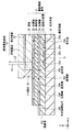
図1は、本実施態様としての反射型液晶表示素子1(以下、単に表示素子1という。)の全体構成を表す平面図である。図2は、表示素子1の要部を表す断面図であり、図1のII−II線に沿った矢視方向の断面を表している。また、図3は、表示素子1の駆動部の構成を表す概略図である。表示素子1は、対向配置された一対の基板間に液晶を封入したアクティブ型の反射型液晶表示素子である。具体的には、対向配置された透明電極基板10および画素電極基板20と、それらの間に挟まれ、シール部材32によって封入された液晶31とを備えたものである。シール部材32は、例えば図1に示したように透明電極基板10の外縁に沿って設けられており、透明電極基板10と画素電極基板20とを接合している。シール部材32によって囲まれた領域は、映像表示を行う表示領域(有効領域)60である。表示領域60には、複数の画素がマトリックス状に配列されている。
<1. Embodiment>
[Overall structure of display element]
FIG. 1 is a plan view showing an overall configuration of a reflective liquid crystal display element 1 (hereinafter simply referred to as a display element 1) according to this embodiment. FIG. 2 is a cross-sectional view illustrating a main part of the display element 1, and illustrates a cross-section in the arrow direction along the line II-II in FIG. FIG. 3 is a schematic diagram showing the configuration of the drive unit of the display element 1. The display element 1 is an active reflection type liquid crystal display element in which liquid crystal is sealed between a pair of substrates arranged opposite to each other. Specifically, the
図3に示したように、駆動部は、各画素内に形成される画素駆動回路61と、表示領域60の周辺に配置される、データドライバ62および走査ドライバ63などのロジック部とを有する。データドライバ62には、信号線64を介して外部からの画像信号Dが入力される。画素駆動回路61は、画素電極25Aの下層に形成され、例えばCMOSやNMOSなどのトランジスタTrと液晶に電圧を供給するキャパシタ(補助容量)Cとを含んでいる。
As shown in FIG. 3, the drive unit includes a
画素駆動回路61においては、列方向(Y軸方向)に延伸する複数のデータ線71が行方向(X軸方向)に並ぶように配置されると共に、行方向に延伸する複数の走査線72が列方向に並ぶように配置されている。各データ線71と各走査線72との交差点が、1画素に対応している。各トランジスタTrのソース電極はデータ線71に接続され、各トランジスタTrのゲート電極は走査線72に接続されている。各トランジスタTrのドレイン電極は、画素電極25Aと補助容量Cとにそれぞれ接続されている。各データ線71は、データドライバ62に接続され、このデータドライバ62から画像信号が供給されるようになっている。各走査線72は、走査ドライバ63に接続され、走査ドライバ63から走査信号が順次供給されるようになっている。なお、駆動部は、このようなアナログ駆動方式に限らず、デジタル駆動方式であってもよい。
In the
透明電極基板10は、ガラスやプラスチックなどの透明材料からなる透明基板11と、この透明基板11の内面、すなわち液晶31と接する面(画素電極基板20と対向する面)に形成された透明電極12とを有している。透明電極12は、表示領域60を全面的に占めるように設けられている。透明電極12の表面には、例えば配向膜(図示せず)が全面的に形成されていてもよい。透明電極12の構成材料としては、例えば酸化すず(SnO2)と酸化インジウム(In2O3)との固溶体物質であるITO(Indium Tin Oxide;インジウムすず酸化膜)などの光の透過作用のある電極材料が用いられる。透明電極12には、全ての画素において共通の電位(例えば接地電位)が印加されるようになっている。
The
画素電極基板20は、例えば単結晶シリコンなどからなる支持基板21の上に、回路形成層22、金属層23、絶縁層24および金属層25が順に積層形成されたものである。図4(A),4(B)は、金属層23,25の平面構成をそれぞれ表す平面図である。
The
回路形成層22における表示領域60には、画素駆動回路61が形成されている。また、回路形成層22における表示領域60を取り囲む周辺領域には、データドライバ62および走査ドライバ63などが形成されている。これらのデータドライバ62および走査ドライバ63は、例えば図5に示したように、所定の数からなる画素群ごとに対応して設けられた複数の回路ブロック60Bを有している。それらの各回路ブロック60Bには、例えばデジタル駆動方式の場合にはデジタル信号をデジタル駆動用の電圧に変換するインターフェイスとしてのLVDS(Low voltage differential signaling)回路などが含まれている。回路形成層22において、画素駆動回路61、データドライバ62および走査ドライバ63は、絶縁膜22Zによって埋設されている。
A
金属層23には、例えば図4(A)に示したように、それぞれ所定形状を有する遮光膜23A、複数の信号線23B、および複数の外部接続端子23Cが、それぞれ所定の位置に設けられている。遮光膜23A、信号線23B、および外部接続端子23Cは、例えばCu(銅)などの、高い導電率を示し、かつ遮光性にも優れた金属材料によって形成されており、それらの間隙を埋める絶縁層23Zによって相互に絶縁されている。遮光膜23Aは、例えば、金属層25に含まれる全ての画素電極25A(後出)と重複する領域、すなわち表示領域を一様に占めるように形成されたベタ膜である。なお、遮光膜23Aは、金属層25の遮光膜25C(後出)と重複する領域をも占めるように形成されていてもよい。遮光膜23Aは、透明電極基板10を透過して画素電極基板20に入射した光のうち画素電極25A同士の間隙を透過した光が、回路形成層22における駆動回路(特にトランジスタTr)に入射するのを防ぐように機能する。信号線23Bは、例えば外部からの画像信号D(後出)や駆動電圧を供給するための配線である。また、外部接続端子23Cは、例えば画素駆動回路61を構成するデータ線71もしくは走査線72と接続されている。
For example, as shown in FIG. 4A, the
金属層25には、例えば図4(B)に示したように、それぞれ所定形状を有する複数の画素電極25Aと遮光膜25B,25Cとが、それぞれ所定の位置に設けられている。
For example, as shown in FIG. 4B, the
画素電極25Aは、XY平面に広がる表示領域60に沿ってマトリックス状に複数配列されている。すなわち、一の画素電極25Aが透明電極12および液晶31などと共に一の画素を構成している。画素電極25Aは、透明電極基板10を透過した光を反射する反射型の画素電極である。すなわち、画素電極25Aは、光反射膜としての機能と、液晶31に電圧を印加する電極として機能との双方を有している。そのため、画素電極25Aは、例えばAl(アルミニウム)や銀(Ag)などの、高い導電率を示し、かつ光反射性能にも優れた金属材料によって形成されている。さらに反射率を上げるために誘電体ミラーのような多層膜による反射層を画素電極25Aの上に積層するようにしてもよい。また、画素電極25Aを保護するため、酸化物あるいは窒化物の膜によって複数の画素電極25Aを全面的に覆うようにしてもよい。
A plurality of
遮光膜25B,25Cは、遮光膜23Aと同様に、回路形成層22における駆動回路(特にトランジスタTr)への光の入射を妨げるものであり、例えば遮光膜23Aもしくは画素電極25Aと同様の金属材料によって形成されている。画素電極25Aおよび遮光膜25B,25Cは、それらの間隙を埋める絶縁層25Zによって相互に絶縁されている。なお、絶縁層25Zにおける金属層23の外部接続端子23Cと対応する領域には開口が設けられており、外部接続端子23Cが露出した状態となっている。
The
遮光膜25Bは、全ての画素電極25Aの周囲を取り囲むように、表示領域60の周辺の領域に形成されている。また、遮光膜25Bは、例えば図5に示したように、回路形成層22における回路ブロック60B同士の境界位置と異なる位置において分割された複数の部分25B1,25B2,・・・によって構成されていることが望ましい。遮光膜25Bは、絶縁層24および絶縁膜25Zと接しており、周囲から電気的に孤立した状態(フローティング状態)となっている。
The
遮光膜25Cは、画素電極25Aと、それを取り囲む遮光膜25Bとの間に形成されており、例えばその上にシール部材32が形成されている。また、遮光膜25Cは、透明電極12と同じ電位を有していることが望ましい。液晶31の内部に意図しない電位差が生じるのを回避し、液晶31の挙動を安定化させるためである。
The
[表示素子の動作]
次に、以上のように構成された表示素子1の動作を説明する。
[Operation of display element]
Next, the operation of the display element 1 configured as described above will be described.
この表示素子1では、透明電極基板10と液晶31とを順次通過した入射光L1を、反射型の画素電極25Aの反射機能により反射させる。画素電極25Aにおいて反射された光L1は、液晶31と透明電極基板10とを順次通過して外部へ射出される。このとき、液晶31は、対向する電極間の電位差(すなわち、画素電極25Aと透明電極12との電位差)に応じてその光学的な特性が変化し、通過する光L1を変調させる。この光変調により階調表現が可能となり、その変調された光L2が映像表示に利用される。
In the display element 1, incident light L1 that sequentially passes through the
液晶31への電圧印加は、図3に示した画素駆動回路61によって行われる。データドライバ62は、信号線64を介して入力された外部からの画像信号Dに応じて、データ線71に画像信号を供給する。走査ドライバ63は、所定のタイミングで各走査線72に走査信号を順次供給する。これにより、走査線72からの走査信号によって走査され、かつデータ線71からの画像信号が印加された部分の画素が選択的に駆動される。
The voltage application to the
[表示素子の作用・効果]
この表示素子1では、回路形成層22の上層として、遮光性もしくは光反射性能を有する画素電極25Aおよび遮光膜25B,25Cを含む金属層25を設けるようにしたので、画素駆動回路61、データドライバ62および走査ドライバ63などへの入射光L1の進入を防止することができる。特に、回路形成層22と金属層25との間に遮光膜23Aを設けるようにしたので、画素電極25A同士の間隙を透過する入射光L1を確実に遮断することができる。よって、駆動部の誤動作を確実に回避することができる。
[Operation and effect of display element]
In the display element 1, since the
ここで、金属層25における遮光膜25Bを周囲から電気的に孤立した状態としたので、例えば製造段階において生じた異物の混入に起因する、画素電極25Aおよび遮光膜25Cと、金属層23における信号線23Bとの短絡を回避することができる。具体的には、例えば図6(A)に示したように、何らかの要因で発生した導電性の異物81が遮光膜25Bから信号線23Bに至るまで突き刺さった場合、遮光膜25Bと信号線23Bとは導通した状態となる。しかしながら、遮光膜25Bを予め電気的に孤立した状態としておくことで、遮光膜25Bと信号線23Bとを同じ電位に安定させることができる。これに対し、例えば図6(B)に示した比較例のように、遮光膜25Bが遮光膜25Cと分離されておらず、透明電極12と同電位であると、異物81の進入によって遮光膜25Bと信号線23Bとの短絡が生じてしまう場合がある(第1の短絡モード)。本実施態様では、このような第1の短絡モードを回避することができる。
Here, since the
なお、上記のように遮光膜25Bを電気的に孤立した状態とした場合であっても、確率は低いながらも、例えば図7(A)に示したように異物混入が複数箇所において同時に生じると、2以上の信号線23B同士が一の遮光膜25Bを介して短絡する可能性がある(第2の短絡モード)。具体的には、図7(A)の比較例において、異物81により信号線23B1と遮光膜25Bとが導通すると共に異物82により信号線23B2と遮光膜25Bとが導通した場合、遮光膜25Bを介して異なる電位の信号線23B1および信号線23B2が短絡することとなる。そこで、本実施態様では遮光膜25Bを複数の部分に分割するようにしたので、このような第2の短絡モードを回避することができる。具体的には図7(B)に示したように、異物81により信号線23B1と遮光膜25B1とが導通すると共に異物82により信号線23B2と遮光膜25B2とが導通した場合であっても、信号線23B1と信号線23B2との短絡は生じない。遮光膜25B1と遮光膜25B2とが絶縁されているからである。さらに、本実施態様では、遮光膜25B同士の境界位置を、回路形成層22に形成された回路ブロック同士の境界位置と異なる位置としたので、回路ブロックの内部への入射光L1の進入をより確実に回避することができる。
Even when the
このように、本実施態様の表示素子1によれば、表示領域60を取り囲む、異物混入が生じやすい周辺領域に形成された遮光膜25Bを電気的に孤立させるようにした。このため、厚さ方向において重なり合う遮光膜25Bと信号線23Bとが異物混入などに起因して相互に導通した場合であっても、短絡による動作不良を回避することができる。また、遮光膜25Bなどにより、不要光の入射による駆動部の動作不良を回避することもできる。よって、全体構成の小型化を実現しつつ、高い動作信頼性を確保することができる。
As described above, according to the display element 1 of this embodiment, the
<2.適用例>
次に、上記した表示素子の適用例について説明する。
<2. Application example>
Next, application examples of the display element described above will be described.
本技術の表示素子は液晶表示装置に適用可能である。ここでは、図8に示したように、反射型液晶表示素子(表示素子1)をライトバルブとして使用した反射型液晶プロジェクタを例示して説明する。 The display element of the present technology can be applied to a liquid crystal display device. Here, as shown in FIG. 8 , a reflective liquid crystal projector using the reflective liquid crystal display element (display element 1) as a light valve will be described as an example.
図8に示した反射型液晶プロジェクタは、赤、緑および青の各色用の液晶ライトバルブ1R,1G,1Bを3枚用いてカラー画像表示を行う、いわゆる3板方式のものである。この反射型液晶プロジェクタは、光軸40に沿って、光源41と、ダイクロイックミラー42,43と、全反射ミラー44とを備えている。この反射型液晶プロジェクタは、さらに、偏光ビームスプリッタ45,46,47と、合成プリズム48と、投射レンズ49と、スクリーン50とを備えている。
The reflective liquid crystal projector shown in FIG. 8 is a so-called three-plate system that displays color images using three liquid
光源41は、カラー画像表示に必要とされる、赤色光(R)、青色光(B)および緑色光(G)を含んだ白色光を発するものであり、例えばハロゲンランプ、メタルハライドランプまたはキセノンランプなどにより構成されている。
The
ダイクロイックミラー42は、光源41からの光を、青色光とその他の色光とに分離する機能を有している。ダイクロイックミラー43は、ダイクロイックミラー42を通過した光を、赤色光と緑色光とに分離する機能を有している。全反射ミラー44は、ダイクロイックミラー42によって分離された青色光を、偏光ビームスプリッタ47に向けて反射するようになっている。
The
偏光ビームスプリッタ45,46,47は、それぞれ、赤色光、緑色光および青色光の光路に沿って設けられている。これらの偏光ビームスプリッタ45,46,47は、それぞれ、偏光分離面45A,46A,47Aを有し、この偏光分離面45A,46A,47Aにおいて、入射した各色光を互いに直交する2つの偏光成分に分離する機能を有している。偏光分離面45A,46A,47Aは、一方の偏光成分(例えばS偏光成分)を反射し、他方の偏光成分(例えばP偏光成分)は透過するようになっている。
The
液晶ライトバルブ1R,1G,1Bは、上述した構成の表示素子1(図1)と同様のものによって構成されている。これらの液晶ライトバルブ1R,1G,1Bには、偏光ビームスプリッタ45,46,47の偏光分離面45A,46A,47Aによって分離された所定の偏光成分(例えばS偏光成分)の色光が入射されるようになっている。液晶ライトバルブ1R,1G,1Bは、画像信号に基づいて与えられた駆動電圧に応じて駆動され、入射光を変調させると共に、その変調された光を偏光ビームスプリッタ45,46,47に向けて反射する機能を有している。
The liquid
合成プリズム48は、液晶ライトバルブ1R,1G,1Bから出射され、偏光ビームスプリッタ45,46,47を通過した所定の偏光成分(例えばP偏光成分)の色光を、合成する機能を有している。投射レンズ49は、合成プリズム48から出射された合成光を、スクリーン50に向けて投射する投射手段としての機能を有している。
The synthesizing
以上のように構成された反射型液晶プロジェクタにおいて、光源41から出射された白色光は、まず、ダイクロイックミラー42の機能によって青色光とその他の色光(赤色光および緑色光)とに分離される。このうち青色光は、全反射ミラー44の機能によって、偏光ビームスプリッタ47に向けて反射される。一方、赤色光および緑色光は、ダイクロイックミラー43の機能によって、さらに、赤色光と緑色光とに分離される。分離された赤色光および緑色光は、それぞれ、偏光ビームスプリッタ45,46に入射される。
In the reflection type liquid crystal projector configured as described above, the white light emitted from the
偏光ビームスプリッタ45,46,47は、入射した各色光を、偏光分離面45A,46A,47Aにおいて、互いに直交する2つの偏光成分に分離する。このとき、偏光分離面45A,46A,47Aは、一方の偏光成分(例えばS偏光成分)を液晶ライトバルブ1R,1G,1Bに向けて反射する。
The
液晶ライトバルブ1R,1G,1Bは、画像信号に基づいて与えられた駆動電圧に応じて駆動され、入射した所定の偏光成分の色光を画素単位で変調させる。このとき、液晶ライトバルブ1R,1G,1Bは、図1に示した表示素子1によって構成されているので、短絡や不要光の入射による動作不良を生じることなく、コンパクトな構成でありながら高い動作信頼性を発揮することができる。
The liquid
液晶ライトバルブ1R,1G,1Bは、変調した各色光を偏光ビームスプリッタ45,46,47に向けて反射する。偏光ビームスプリッタ45,46,47は、液晶ライトバルブ1R,1G,1Bからの反射光(変調光)のうち、所定の偏光成分(例えばP偏光成分)のみを通過させ、合成プリズム48に向けて出射する。合成プリズム48は、偏光ビームスプリッタ45,46,47を通過した所定の偏光成分の色光を合成し、投射レンズ49に向けて出射する。投射レンズ49は、合成プリズム48から出射された合成光を、スクリーン50に向けて投射する。これにより、スクリーン50に、液晶ライトバルブ1R,1G,1Bによって変調された光に応じた映像が投影され、所望の映像表示がなされる。
The liquid
以上説明したように、本実施態様に係る反射型液晶プロジェクタによれば、上記実施態様で説明した表示素子(図1)を、液晶ライトバルブ1R,1G,1Bとして用いるようにしたので、全体構成の小型化を図りつつ、高い動作信頼性を確保することができる。
As described above, according to the reflective liquid crystal projector according to this embodiment, the display element (FIG. 1) described in the above embodiment is used as the liquid
以上、実施態様を挙げて本技術を説明したが、本技術はこれらの実施態様等には限定されず、種々の変形が可能である。例えば上記実施態様では、画素電極基板20において、最上層に位置する金属層25に含まれる遮光膜25Bを電気的に孤立させるようにしたが、本技術はこれに限定されるものではない。例えば、金属層25の下方に位置する金属層23において電気的に孤立した金属膜を設けるようにしてもよい。すなわち、例えば図2において、金属層25が信号線23Bに相当する金属膜を含むようにすると共に、金属層23が遮光膜25Bに相当する金属膜を含むようにしてもよい。
While the present technology has been described with reference to the embodiments, the present technology is not limited to these embodiments and the like, and various modifications are possible. For example, in the above embodiment, in the
また、上記実施態様では、金属層25における遮光膜25Bを、信号線23Bの延伸方向において複数に分割するようにしたが、本技術はこれに限定されるものではなく適宜変更可能なものである。例えば、図9(A),9(B)に示したように、複数の信号線23Bが並ぶ方向において分割するようにしてもよい。そうすることにより、短絡発生の確率をよりいっそう低減することができる。
Moreover, in the said embodiment, although the
また、本技術は以下のような構成を取り得るものである。
(1)
透明基板と、その一方の面に形成された透明電極とを有する透明電極基板と、
液晶層と、
前記液晶層を挟んで前記透明電極と対向する領域に位置する複数の画素電極、およびそれ以外の領域に位置する第1の導電膜を含む第1の層と、前記第1の導電膜と重複する領域に位置する第2の導電膜を含む第2の層とを順に有する画素電極基板と
を備え、
前記第1および第2の導電膜の少なくとも一方が電気的に孤立している
液晶表示素子。
(2)
前記画素電極は、前記透明電極基板を透過した光を反射する導電材料からなる
上記(1)記載の液晶表示素子。
(3)
前記第1の導電膜は、前記複数の画素電極の周囲を取り囲むように形成されている
上記(1)または(2)に記載の液晶表示素子。
(4)
前記画素電極基板は、前記第2の層の前記透明電極基板と反対側に、前記画素電極と接続された駆動素子を複数含む回路形成層を有する
上記(1)から(3)のいずれか1つに記載の液晶表示素子。
(5)
前記回路形成層は、前記駆動素子としてのトランジスタをそれぞれ含む複数の回路ブロックが形成されている
上記(4)記載の液晶表示素子。
(6)
前記第1および第2の導電膜のうちの少なくとも一方は遮光性を有する
上記(5)記載の液晶表示素子。
(7)
前記第1および第2の導電膜のうちの少なくとも一方は、前記回路ブロック同士の境界位置と異なる位置において分割された複数の部分からなる
上記(6)記載の液晶表示素子。
(8)
前記第1の層は、前記第1の導電膜と前記画素電極との間に形成された第1の遮光膜を含む
上記(1)から(7)のいずれか1つに記載の液晶表示素子。
(9)
前記画素電極基板は、前記第1の遮光膜に設けられたシール部材によって前記透明電極基板と接合されている
上記(8)記載の液晶表示素子。
(10)
前記画素電極、第1の遮光膜および第1の導電膜は、全て同一材料からなり、互いに絶縁されている
上記(8)または(9)に記載の液晶表示素子。
(11)
前記第1の遮光膜は、前記透明電極と同じ電位を有する
上記(8)から(10)のいずれか1つに記載の液晶表示素子。
(12)
前記第2の層は、前記複数の画素電極と重複する領域に形成された第2の遮光膜を含む
上記(1)から(11)のいずれか1つに記載の液晶表示素子。
(13)
光源と、
上記(1)から(12)のいずれか1つに記載の液晶表示素子と、
前記光源から発せられ、前記液晶表示素子によって変調された光をスクリーンに投影する投影部と
を備えた液晶表示装置。
Moreover, this technique can take the following structures.
(1)
A transparent electrode substrate having a transparent substrate and a transparent electrode formed on one surface thereof;
A liquid crystal layer;
A first layer including a plurality of pixel electrodes located in a region facing the transparent electrode with the liquid crystal layer interposed therebetween, and a first conductive film located in a region other than the pixel electrode, and overlapping with the first conductive film A pixel electrode substrate having a second layer including a second conductive film located in a region to be sequentially arranged,
A liquid crystal display element, wherein at least one of the first and second conductive films is electrically isolated.
(2)
The liquid crystal display element according to (1), wherein the pixel electrode is made of a conductive material that reflects light transmitted through the transparent electrode substrate.
(3)
The liquid crystal display element according to (1) or (2), wherein the first conductive film is formed so as to surround a periphery of the plurality of pixel electrodes.
(4)
The pixel electrode substrate has a circuit formation layer including a plurality of driving elements connected to the pixel electrode on the opposite side of the second layer to the transparent electrode substrate. Any one of (1) to (3) The liquid crystal display element described in 1.
(5)
The liquid crystal display element according to (4), wherein the circuit forming layer includes a plurality of circuit blocks each including a transistor as the driving element.
(6)
The liquid crystal display element according to (5), wherein at least one of the first and second conductive films has a light shielding property.
(7)
The liquid crystal display element according to (6), wherein at least one of the first and second conductive films includes a plurality of portions divided at positions different from a boundary position between the circuit blocks.
(8)
The liquid crystal display element according to any one of (1) to (7), wherein the first layer includes a first light-shielding film formed between the first conductive film and the pixel electrode. .
(9)
The liquid crystal display element according to (8), wherein the pixel electrode substrate is bonded to the transparent electrode substrate by a sealing member provided on the first light shielding film.
(10)
The liquid crystal display element according to (8) or (9), wherein the pixel electrode, the first light shielding film, and the first conductive film are all made of the same material and insulated from each other.
(11)
The liquid crystal display element according to any one of (8) to (10), wherein the first light shielding film has the same potential as the transparent electrode.
(12)
The liquid crystal display element according to any one of (1) to (11), wherein the second layer includes a second light-shielding film formed in a region overlapping with the plurality of pixel electrodes.
(13)
A light source;
The liquid crystal display element according to any one of (1) to (12) above;
A liquid crystal display device comprising: a projection unit that projects light emitted from the light source and modulated by the liquid crystal display element onto a screen.
1…反射型液晶表示素子、10…透明電極基板、11…透明基板、12…透明電極、20…画素電極基板、22…回路形成層、23,25…金属層、23A…遮光膜、23B…信号線、25A…画素電極、25B…遮光膜、31…液晶、60…表示領域、61…画素駆動回路。 DESCRIPTION OF SYMBOLS 1 ... Reflective type liquid crystal display element, 10 ... Transparent electrode substrate, 11 ... Transparent substrate, 12 ... Transparent electrode, 20 ... Pixel electrode substrate, 22 ... Circuit formation layer, 23, 25 ... Metal layer, 23A ... Light shielding film, 23B ... Signal line, 25A ... pixel electrode, 25B ... light shielding film, 31 ... liquid crystal, 60 ... display region, 61 ... pixel drive circuit.
Claims (12)
液晶層と、
前記液晶層を挟んで前記透明電極と対向する表示領域に位置する複数の画素電極、および前記表示領域以外の周辺領域に位置する複数の第1の導電膜を含む第1の層と、前記第1の導電膜と重複する領域に位置する複数の第2の導電膜を含む第2の層とを順に有する画素電極基板と
を備え、
前記複数の第2の導電膜は、それぞれ第1の方向に延在すると共に前記第1の方向と直交する第2の方向において互いに離間して並んでおり、
前記複数の第1の導電膜は、前記第1の方向において互いに離間して並んでおり、
前記複数の第1の導電膜がそれぞれ電気的に孤立しており、
前記画素電極基板は、前記第2の層の前記透明電極基板と反対側に、前記画素電極と接続された駆動素子を複数含む回路形成層を有する
液晶表示素子。 A transparent electrode substrate having a transparent substrate and a transparent electrode formed on one surface thereof;
A liquid crystal layer;
A first layer including a plurality of pixel electrodes located in a display area facing the transparent electrode across the liquid crystal layer, and a plurality of first conductive films located in a peripheral area other than the display area; A pixel electrode substrate having a second layer including a plurality of second conductive films located in a region overlapping with the first conductive film in order,
The plurality of second conductive films each extend in a first direction and are spaced apart from each other in a second direction orthogonal to the first direction,
The plurality of first conductive films are spaced apart from each other in the first direction,
Each of the plurality of first conductive films is electrically isolated ;
The liquid crystal display element , wherein the pixel electrode substrate has a circuit forming layer including a plurality of driving elements connected to the pixel electrode on the opposite side of the second layer to the transparent electrode substrate .
請求項1記載の液晶表示素子。 The circuit-forming layer, a liquid crystal display device according to claim 1, wherein the plurality of circuit blocks are formed each including transistors as the driving element.
請求項2記載の液晶表示素子。 The liquid crystal display element according to claim 2, wherein at least one of the first conductive film and the second conductive film has a light shielding property.
請求項3記載の液晶表示素子。 The liquid crystal display element according to claim 3 , wherein at least one of a boundary position between the plurality of first conductive films and a boundary position between the plurality of second conductive films is different from a boundary position between the circuit blocks.
請求項1から請求項4のいずれか1項に記載の液晶表示素子。 The liquid crystal display element according to any one of claims 1 to 4 , wherein the pixel electrode is made of a conductive material that reflects light transmitted through the transparent electrode substrate.
請求項1から請求項5のいずれか1項に記載の液晶表示素子。 It said plurality of first conductive film, a liquid crystal display device according to any one of claims 1 to 5 which is formed so as to surround the plurality of pixel electrodes.
請求項1から請求項6のいずれか1項に記載の液晶表示素子。 Said first layer, the liquid crystal display device as claimed in any one of claims 6 including the first light shielding film formed between the pixel electrode and the first conductive film.
請求項7記載の液晶表示素子。 The liquid crystal display element according to claim 7 , wherein the pixel electrode substrate is bonded to the transparent electrode substrate by a sealing member provided on the first light shielding film.
請求項7または請求項8に記載の液晶表示素子。 The pixel electrode, the first light shielding film and the first conductive film are all made of the same material, the liquid crystal display device according to claim 7 or claim 8 are insulated from each other.
請求項7から請求項9のいずれか1項に記載の液晶表示素子。 The first light-shielding film has the same potential as the transparent electrode
The liquid crystal display element according to claim 7 .
請求項1から請求項10のいずれか1項に記載の液晶表示素子。 The second layer, the liquid crystal display device as claimed in any one of claims 10, including a second light shielding film formed in a region that overlaps with the plurality of pixel electrodes.
液晶表示素子と、
前記光源から発せられ、前記液晶表示素子によって変調された光をスクリーンに投影する投影部と
を備え、
前記液晶表示素子は、
透明基板と、その一方の面に形成された透明電極とを有する透明電極基板と、
液晶層と、
前記液晶層を挟んで前記透明電極と対向する表示領域に位置する複数の画素電極、および前記表示領域以外の周辺領域に位置する複数の第1の導電膜を含む第1の層と、前記第1の導電膜と重複する領域に位置する複数の第2の導電膜を含む第2の層とを順に有する画素電極基板と
を備え、
前記複数の第2の導電膜は、それぞれ第1の方向に延在すると共に前記第1の方向と直交する第2の方向において互いに離間して並んでおり、
前記複数の第1の導電膜は、前記第1の方向において互いに離間して並んでおり、
前記複数の第1の導電膜がそれぞれ電気的に孤立しており、
前記画素電極基板は、前記第2の層の前記透明電極基板と反対側に、前記画素電極と接続された駆動素子を複数含む回路形成層を有する
液晶表示装置。
A light source;
A liquid crystal display element;
A projection unit that projects light emitted from the light source and modulated by the liquid crystal display element onto a screen;
The liquid crystal display element is
A transparent electrode substrate having a transparent substrate and a transparent electrode formed on one surface thereof;
A liquid crystal layer;
A first layer including a plurality of pixel electrodes located in a display area facing the transparent electrode across the liquid crystal layer, and a plurality of first conductive films located in a peripheral area other than the display area; A pixel electrode substrate having a second layer including a plurality of second conductive films located in a region overlapping with the first conductive film in order,
The plurality of second conductive films each extend in a first direction and are spaced apart from each other in a second direction orthogonal to the first direction,
The plurality of first conductive films are spaced apart from each other in the first direction,
Each of the plurality of first conductive films is electrically isolated ;
The liquid crystal display device , wherein the pixel electrode substrate has a circuit forming layer including a plurality of drive elements connected to the pixel electrode on the opposite side of the second layer to the transparent electrode substrate .
Priority Applications (2)
| Application Number | Priority Date | Filing Date | Title |
|---|---|---|---|
| JP2011207987A JP6014978B2 (en) | 2011-09-22 | 2011-09-22 | Liquid crystal display element and liquid crystal display device |
| US13/608,048 US9664947B2 (en) | 2011-09-22 | 2012-09-10 | Liquid crystal display device and liquid crystal display |
Applications Claiming Priority (1)
| Application Number | Priority Date | Filing Date | Title |
|---|---|---|---|
| JP2011207987A JP6014978B2 (en) | 2011-09-22 | 2011-09-22 | Liquid crystal display element and liquid crystal display device |
Publications (3)
| Publication Number | Publication Date |
|---|---|
| JP2013068838A JP2013068838A (en) | 2013-04-18 |
| JP2013068838A5 JP2013068838A5 (en) | 2014-10-02 |
| JP6014978B2 true JP6014978B2 (en) | 2016-10-26 |
Family
ID=47910925
Family Applications (1)
| Application Number | Title | Priority Date | Filing Date |
|---|---|---|---|
| JP2011207987A Expired - Fee Related JP6014978B2 (en) | 2011-09-22 | 2011-09-22 | Liquid crystal display element and liquid crystal display device |
Country Status (2)
| Country | Link |
|---|---|
| US (1) | US9664947B2 (en) |
| JP (1) | JP6014978B2 (en) |
Families Citing this family (11)
| Publication number | Priority date | Publication date | Assignee | Title |
|---|---|---|---|---|
| JP6102646B2 (en) | 2013-01-23 | 2017-03-29 | ソニー株式会社 | Input device, electronic device and sensor sheet |
| JP6119518B2 (en) | 2013-02-12 | 2017-04-26 | ソニー株式会社 | Sensor device, input device and electronic apparatus |
| CN105190492B (en) | 2013-03-18 | 2019-09-27 | 索尼公司 | Sensor device, input unit and electronic equipment |
| JP6245257B2 (en) | 2013-04-04 | 2017-12-13 | ソニー株式会社 | Input device and electronic device |
| JP6142745B2 (en) | 2013-09-10 | 2017-06-07 | ソニー株式会社 | Sensor device, input device and electronic apparatus |
| JP2015185281A (en) | 2014-03-20 | 2015-10-22 | ソニー株式会社 | Key board cover and electronic apparatus |
| JP2015190859A (en) | 2014-03-28 | 2015-11-02 | ソニー株式会社 | Sensor device, input device, and electronic apparatus |
| JP2017009637A (en) * | 2015-06-17 | 2017-01-12 | 株式会社ジャパンディスプレイ | Liquid crystal display device |
| JP6631646B2 (en) * | 2018-02-27 | 2020-01-15 | セイコーエプソン株式会社 | Electro-optical devices and electronic equipment |
| JP7158899B2 (en) * | 2018-06-06 | 2022-10-24 | 株式会社ジャパンディスプレイ | electro-optical device |
| JP7028236B2 (en) * | 2019-12-05 | 2022-03-02 | セイコーエプソン株式会社 | Electro-optics and electronic devices |
Family Cites Families (27)
| Publication number | Priority date | Publication date | Assignee | Title |
|---|---|---|---|---|
| US6081305A (en) * | 1995-05-30 | 2000-06-27 | Hitachi, Ltd. | Liquid crystal light valve and projection type liquid crystal display using such valve |
| JP3513410B2 (en) * | 1998-12-24 | 2004-03-31 | キヤノン株式会社 | Image display device |
| JP3428511B2 (en) * | 1999-07-02 | 2003-07-22 | 日本電気株式会社 | Active matrix type liquid crystal display |
| US7432994B2 (en) * | 2003-11-20 | 2008-10-07 | Chunghwa Picture Tubes, Ltd. | Liquid crystal display device and fabrication method thereof |
| KR100964797B1 (en) * | 2003-12-23 | 2010-06-21 | 엘지디스플레이 주식회사 | Liquid Crystal Display Device and the fabrication method thereof |
| JP4058766B2 (en) * | 2004-03-23 | 2008-03-12 | ソニー株式会社 | Reflective liquid crystal display element and liquid crystal display device |
| JP2006267937A (en) * | 2005-03-25 | 2006-10-05 | Victor Co Of Japan Ltd | Reflection type liquid crystal display device |
| JP4386066B2 (en) | 2006-01-17 | 2009-12-16 | ソニー株式会社 | Wiring structure for display device and projection display device |
| US7439565B2 (en) * | 2006-06-08 | 2008-10-21 | Chunghwa Picture Tubes, Ltd. | Active devices array substrate and repairing method thereof |
| KR101252001B1 (en) * | 2006-06-15 | 2013-04-08 | 삼성디스플레이 주식회사 | Liquid crystal display and method of manufacturing thereof |
| TWI409778B (en) * | 2008-12-25 | 2013-09-21 | Innolux Corp | Liquid crystal display apparatus, liquid crystal display panel and driving method |
| JP5347913B2 (en) | 2009-11-06 | 2013-11-20 | ソニー株式会社 | SENSOR DEVICE, ELECTRONIC DEVICE, AND METHOD FOR MANUFACTURING SENSOR DEVICE |
| JP2011222167A (en) | 2010-04-06 | 2011-11-04 | Sony Corp | Transparent conducting film and photoelectric conversion device |
| KR101065323B1 (en) * | 2010-05-24 | 2011-09-16 | 삼성모바일디스플레이주식회사 | Liquid crystal display device |
| TW201200948A (en) * | 2010-06-22 | 2012-01-01 | Au Optronics Corp | Pixel structure and method for manufacturing the same |
| JP5853419B2 (en) * | 2010-10-25 | 2016-02-09 | セイコーエプソン株式会社 | Electro-optical device, electronic apparatus, and substrate for electro-optical device |
| JP2012103797A (en) | 2010-11-08 | 2012-05-31 | Sony Corp | Input device, coordinate detection method and program |
| JP5299872B2 (en) * | 2010-11-30 | 2013-09-25 | 株式会社ジャパンディスプレイ | Liquid crystal display |
| JP6016228B2 (en) | 2012-07-03 | 2016-10-26 | ソニーセミコンダクタソリューションズ株式会社 | Sensor device |
| JP6102646B2 (en) | 2013-01-23 | 2017-03-29 | ソニー株式会社 | Input device, electronic device and sensor sheet |
| JP6119518B2 (en) | 2013-02-12 | 2017-04-26 | ソニー株式会社 | Sensor device, input device and electronic apparatus |
| US20160011691A1 (en) | 2013-03-13 | 2016-01-14 | Sony Corporation | Sensor device, input device, and electronic apparatus |
| CN105190492B (en) | 2013-03-18 | 2019-09-27 | 索尼公司 | Sensor device, input unit and electronic equipment |
| JP6245257B2 (en) | 2013-04-04 | 2017-12-13 | ソニー株式会社 | Input device and electronic device |
| JP6142745B2 (en) | 2013-09-10 | 2017-06-07 | ソニー株式会社 | Sensor device, input device and electronic apparatus |
| JP2015190859A (en) | 2014-03-28 | 2015-11-02 | ソニー株式会社 | Sensor device, input device, and electronic apparatus |
| JP2015194948A (en) | 2014-03-31 | 2015-11-05 | ソニー株式会社 | Information processor, input device, information processing method and program |
-
2011
- 2011-09-22 JP JP2011207987A patent/JP6014978B2/en not_active Expired - Fee Related
-
2012
- 2012-09-10 US US13/608,048 patent/US9664947B2/en active Active
Also Published As
| Publication number | Publication date |
|---|---|
| US9664947B2 (en) | 2017-05-30 |
| JP2013068838A (en) | 2013-04-18 |
| US20130076994A1 (en) | 2013-03-28 |
Similar Documents
| Publication | Publication Date | Title |
|---|---|---|
| JP6014978B2 (en) | Liquid crystal display element and liquid crystal display device | |
| JP5786601B2 (en) | Electro-optical device and electronic apparatus | |
| JP6244802B2 (en) | Electro-optical device and electronic apparatus | |
| US9575371B2 (en) | Liquid crystal device and electronic apparatus | |
| JP6079077B2 (en) | Electro-optical device, method of manufacturing electro-optical device, and electronic apparatus | |
| US10761384B2 (en) | Electro-optical device and electronic apparatus | |
| JP4058766B2 (en) | Reflective liquid crystal display element and liquid crystal display device | |
| US10847741B2 (en) | Electro-optical device, manufacturing method for electro-optical device, and electronic apparatus | |
| US11662640B2 (en) | Electro-optical device with interlayer insulating layers and contact holes, and electronic apparatus | |
| JP2019184937A (en) | Electro-optic device, electronic apparatus, and method for manufacturing electro-optic device | |
| US20200312890A1 (en) | Electro-optical device and electronic apparatus | |
| JP2009122305A (en) | Liquid crystal device and electronic device | |
| JP2018045018A (en) | Liquid crystal device and electronic apparatus | |
| JP2012181308A (en) | Electro-optical device and electronic device | |
| JP2011191475A (en) | Electro-optic device and method for manufacturing the same, and electronic equipment | |
| US20190129263A1 (en) | Electro-optical device and electronic apparatus | |
| JP2020086343A (en) | Electro-optic device and electronic apparatus | |
| JP7447724B2 (en) | Electro-optical devices and electronic equipment | |
| JP7028236B2 (en) | Electro-optics and electronic devices | |
| JP2018163190A (en) | Electro-optical device, electronic apparatus, and manufacturing method for electro-optical device | |
| JP7409236B2 (en) | Electro-optical devices and electronic equipment | |
| US11899324B2 (en) | Electro-optical device and display apparatus | |
| US20230328210A1 (en) | Electro-optical device and display apparatus | |
| JP7028281B2 (en) | Electro-optics and electronic devices | |
| US20220413328A1 (en) | Electro-optical device and electronic apparatus |
Legal Events
| Date | Code | Title | Description |
|---|---|---|---|
| A521 | Request for written amendment filed |
Free format text: JAPANESE INTERMEDIATE CODE: A523 Effective date: 20140815 |
|
| A621 | Written request for application examination |
Free format text: JAPANESE INTERMEDIATE CODE: A621 Effective date: 20140815 |
|
| A977 | Report on retrieval |
Free format text: JAPANESE INTERMEDIATE CODE: A971007 Effective date: 20150522 |
|
| A131 | Notification of reasons for refusal |
Free format text: JAPANESE INTERMEDIATE CODE: A131 Effective date: 20150701 |
|
| A521 | Request for written amendment filed |
Free format text: JAPANESE INTERMEDIATE CODE: A523 Effective date: 20150821 |
|
| A131 | Notification of reasons for refusal |
Free format text: JAPANESE INTERMEDIATE CODE: A131 Effective date: 20160301 |
|
| A521 | Request for written amendment filed |
Free format text: JAPANESE INTERMEDIATE CODE: A523 Effective date: 20160420 |
|
| TRDD | Decision of grant or rejection written | ||
| A01 | Written decision to grant a patent or to grant a registration (utility model) |
Free format text: JAPANESE INTERMEDIATE CODE: A01 Effective date: 20160830 |
|
| A61 | First payment of annual fees (during grant procedure) |
Free format text: JAPANESE INTERMEDIATE CODE: A61 Effective date: 20160912 |
|
| R151 | Written notification of patent or utility model registration |
Ref document number: 6014978 Country of ref document: JP Free format text: JAPANESE INTERMEDIATE CODE: R151 |
|
| R250 | Receipt of annual fees |
Free format text: JAPANESE INTERMEDIATE CODE: R250 |
|
| R250 | Receipt of annual fees |
Free format text: JAPANESE INTERMEDIATE CODE: R250 |
|
| LAPS | Cancellation because of no payment of annual fees |