EP3042293B1 - Periodisches training für empfänger ungleicher signale - Google Patents
Periodisches training für empfänger ungleicher signale Download PDFInfo
- Publication number
- EP3042293B1 EP3042293B1 EP14843012.7A EP14843012A EP3042293B1 EP 3042293 B1 EP3042293 B1 EP 3042293B1 EP 14843012 A EP14843012 A EP 14843012A EP 3042293 B1 EP3042293 B1 EP 3042293B1
- Authority
- EP
- European Patent Office
- Prior art keywords
- training
- memory device
- memory
- controller
- signal
- Prior art date
- Legal status (The legal status is an assumption and is not a legal conclusion. Google has not performed a legal analysis and makes no representation as to the accuracy of the status listed.)
- Active
Links
Images



Classifications
-
- G—PHYSICS
- G05—CONTROLLING; REGULATING
- G05B—CONTROL OR REGULATING SYSTEMS IN GENERAL; FUNCTIONAL ELEMENTS OF SUCH SYSTEMS; MONITORING OR TESTING ARRANGEMENTS FOR SUCH SYSTEMS OR ELEMENTS
- G05B13/00—Adaptive control systems, i.e. systems automatically adjusting themselves to have a performance which is optimum according to some preassigned criterion
- G05B13/02—Adaptive control systems, i.e. systems automatically adjusting themselves to have a performance which is optimum according to some preassigned criterion electric
-
- G—PHYSICS
- G06—COMPUTING OR CALCULATING; COUNTING
- G06N—COMPUTING ARRANGEMENTS BASED ON SPECIFIC COMPUTATIONAL MODELS
- G06N20/00—Machine learning
-
- G—PHYSICS
- G11—INFORMATION STORAGE
- G11C—STATIC STORES
- G11C29/00—Checking stores for correct operation ; Subsequent repair; Testing stores during standby or offline operation
- G11C29/02—Detection or location of defective auxiliary circuits, e.g. defective refresh counters
- G11C29/022—Detection or location of defective auxiliary circuits, e.g. defective refresh counters in I/O circuitry
-
- G—PHYSICS
- G11—INFORMATION STORAGE
- G11C—STATIC STORES
- G11C29/00—Checking stores for correct operation ; Subsequent repair; Testing stores during standby or offline operation
- G11C29/02—Detection or location of defective auxiliary circuits, e.g. defective refresh counters
- G11C29/028—Detection or location of defective auxiliary circuits, e.g. defective refresh counters with adaption or trimming of parameters
-
- G—PHYSICS
- G11—INFORMATION STORAGE
- G11C—STATIC STORES
- G11C7/00—Arrangements for writing information into, or reading information out from, a digital store
- G11C7/10—Input/output [I/O] data interface arrangements, e.g. I/O data control circuits, I/O data buffers
- G11C7/1078—Data input circuits, e.g. write amplifiers, data input buffers, data input registers, data input level conversion circuits
- G11C7/1093—Input synchronization
-
- G—PHYSICS
- G11—INFORMATION STORAGE
- G11C—STATIC STORES
- G11C29/00—Checking stores for correct operation ; Subsequent repair; Testing stores during standby or offline operation
- G11C29/04—Detection or location of defective memory elements, e.g. cell constructio details, timing of test signals
- G11C2029/0409—Online test
-
- G—PHYSICS
- G11—INFORMATION STORAGE
- G11C—STATIC STORES
- G11C2207/00—Indexing scheme relating to arrangements for writing information into, or reading information out from, a digital store
- G11C2207/22—Control and timing of internal memory operations
- G11C2207/2254—Calibration
Definitions
- Embodiments of the invention are generally related to memory device writes, and more particularly to periodic training for timing control for writes in an unmatched architecture.
- I/O input/output
- standards e.g., between components of a memory subsystem.
- the I/O standards can relate to performance characteristics for I/O power, I/O latency, and I/O frequency.
- the standards or nominal values of I/O performance settings are set to values that can be achieved across different systems for compatibility and interoperability.
- power and latency there are tradeoffs between power and latency.
- using tight timing parameters can reduce power, but causes the I/O latency to be more negatively affected by temperature, voltage, and process variation.
- FIG. 1A is a block diagram of a known matched receiver circuit.
- amplifier 122 of the data path is matched to both amplifier 124 and clock distribution network 130 of the strobe path.
- the data path includes data input DQ[7:0] input into amplifier 122 with internal Vref signal 110.
- the data strobe path includes inputs for a strobe for p-type devices (DQS_P) and for a strobe for n-type devices (DQS_N).
- Amplifier 124 feeds into clock distribution network 130, which provides a network to distribute the clock signal to multiple recipient devices at the same time. Specifically shown is a signal going to elements 142 and 144 of sampling circuit 140.
- FIG. 1B is a block diagram of a known unmatched receiver circuit.
- unmatched architecture 104 the data (DQ) voltage is sampled directly at the pad. After being sampled, the system can amplify the signal without the tight timing constraints needed for matched architecture 102. Namely, amplification can occur over an entire UI (unit interval) or possibly more. Thus, the gain/bandwidth requirements of the unmatched receiver are lower than that of the matched receiver.
- DQ[7:0] and internal Vref 110 are fed directly to elements 162 and 164 of sampling circuit 160.
- the DQS path still requires a continuous time amplifier, amplifier 126, but the swing on DQS is typically larger than the swing on DQ, which means a lower gain amplifier 126 can be used, as it does not have to be matched to a high gain amplifier in the data path.
- Unmatched architecture 104 improves certain receiver bandwidth and voltage sensitivities with respect to matched architecture 102, but degrades the timing control.
- the delay on the DQS and DQ paths are not self-compensating in unmatched architecture 104.
- any change in TDQS, or the time to propagate a strobe signal through clock distribution network 130 will directly degrade the receiver timing budget.
- Existing training can correct the timing once, but any drift from the trained position will directly affect timing margin. Drift can occur across voltage, temperature, and/or aging, which will degrade timing margins and possibly create link failures.
- Periodic training is known in which training data is written across the link (e.g., from a memory controller to a DRAM (dynamic random access memory)) and checked for errors.
- periodic training suffers from complexity and load on the bus bandwidth. Additionally, the training would be most effective if a large number of samples were averaged, but averaging more samples directly conflicts with performance requirements and feedback loop bandwidth.
- known periodic training is inherently slow because of the iterative nature of the feedback loop of existing training methods.
- WO 2005/072355 A2 relates to data sampling clock edge placement training for high speed GPU-memory interface. It discloses training a phase shift circuit to provide a phase shift for improved data recovery. It provides a variable delay cell. A delay through the variable delay cell is changed while training patterns are received. The presence of errors in the received data pattern is tracked, and from the presence or absence of errors a preferred delay is selected and used for receiving data.
- WO 99/46775 A2 are known an apparatus and method for concurrently refreshing first and second rows of memory cells in a dynamic random access memory (DRAM) component that includes a plurality of banks of memory cells organized in rows.
- a command interface in the DRAM component receives activate request and precharge requests.
- a row register in the DRAM component indicates a row in the DRAM component.
- Logic in the DRAM component activates the row indicated by the row register in response to an activate request and precharges the row in response to a precharge request, the row being in a bank indicated by the activate request and by the precharge request.
- a pseudo random bit stream generator which has a fully programmable pseudo random polynomial up to the supported width of the CSRs, fully programmable tap selection for providing any specified combination of generator state taps, and fully programmable parallel sequence generation which determines the number of sequential bits calculated and how much the sequence generator advances per clock.
- a system for communicating data between a first integrated circuit device and a second integrated circuit device The first integrated circuit device transmits a timing signal to the second integrated circuit device, wherein the timing signal includes a first transition and a second transition. The first integrated circuit device then delays the data, so that the data is delayed relative to the timing signal by a first predetermined delay time. Next, the first integrated circuit device transmits the delayed data to the second integrated circuit device, which receives the timing signal and the delayed data. Next, the second integrated circuit device delays the first transition of the timing signal by a second predetermined delay time to generate a delayed version of the first transition. The second integrated circuit device then senses the data during a time interval between the delayed version of the first transition and the second transition.
- periodic training in a memory subsystem is performed during a training state or training mode.
- the training state is during a refresh cycle of the memory device.
- the memory device and/or memory controller can determine when to place the memory device in the training state or training mode to reduce performance effects of the training.
- the memory subsystem can train the I/O (input/output) during a time that will either not affect the performance of the memory device, or have a low effect on performance. For example, if the training is performed during a refresh state of the memory device, there may be no performance effect seeing that no read or write commands are issued to the memory device during refresh.
- I/O parameters are adjusted based on a number of errors detected in a received training signal.
- a controller device sends the training signal, and the memory device samples the training signal.
- the controller can be a central processing unit (CPU), memory controller, or other processor in the system.
- the memory device can be a single device, or configured in parallel with other memory devices.
- the system can adjust at least one I/O parameter. Either the controller or the memory device can perform the error detection, depending on the configuration of the system. Either an I/O parameter of the controller or an I/O parameter of the memory device can be adjusted, depending on the configuration of the system.
- a system can periodically track drift in the timing associated with a sampling strobe signal, T DQS , over time.
- Periodic compensation can allow the system to keep the sampling strobe signal (DQS) in the middle of the eye of the data signal (DQ).
- Periodic compensation training should be understood as supplemental and in addition to initial training or centering of the DQS signal on the DQ eye.
- the initial training is commonly performed via a process of a BIOS (basic input/output system) that boots and initializes the system in which the memory device and controller are located.
- BIOS basic input/output system
- the initial training can be assumed to be completed, and the periodic compensation training can track and compensate for drift in T DQS .
- Drift typically occurs due to changes in environmental conditions, such as temperature and/or voltage changes during operation of the system. Additionally, aging of the device can cause changes in performance of the device.
- the system can use a simple training pattern (e.g., 1010) for the periodic training.
- a simple training pattern should be sufficient to identify drift in the strobe signal relative to the data signal.
- the controller or transmitting device controls the training operations.
- the controller can separately track values that provide information on the data signal.
- the system employs phase interpolation to sub-divide the activity happening during each phase of the system clock. These values provide information about the specific location of the data signal and/or the strobe signal within the clock cycle.
- the logic used to track the phases can be referred to as a phase interpolator (PI), and values derived from the logic can be referred to as PI values.
- Typical sub-divisions can be 8, 16, or 32, but other binary values can be used.
- the controller separately tracks two PI values.
- One PI indicates conditions for normal operation, and represents the eye center for a worst case training pattern (e.g., as determined during initialization training).
- a second PI value indicates conditions with respect to the periodic training used to track an eye edge.
- the control logic e.g., at the controller, memory device, or some combination
- the control logic can detect how much the DQ edge moves relative to a previously stored value. Based on how much the edge moved, the control logic can determine how to offset the DQ center value. If the DQ edge is based on the training pattern, it should accurately capture the average DQ movements.
- the system can monitor the write path of an I/O interface from a controller to a memory device.
- the monitoring can provide details on the performance of the I/O interface.
- the system can generate enough samples to average to filter noise in the errors, with minimal impact to effective bus bandwidth.
- a test system or test engine can be used to test memory subsystems, and more specifically, the I/O (input/output) interface or communication between a platform component (e.g., a processor, a memory controller) and a memory device.
- the testing can implement the periodic testing described.
- Any memory subsystem that uses a memory controller with a scheduler or equivalent logic can implement at least one embodiment of a test engine.
- Reference made herein to memory devices can include different memory types. For example, memory subsystems commonly use DRAM, which is one example of a memory device as described herein.
- test engine described herein is compatible with any of a number of memory technologies, such as DDR3 (dual data rate version 3, original release by JEDEC (Joint Electronic Device Engineering Council) on June 27, 2007, currently on release 21), DDR4 (DDR version 4, initial specification published in September 2012 by JEDEC), LPDDR4 (low power dual data rate version 4, specification in development by JEDEC as of the filing of this application), WIO (Wide I/O, specification in development by JEDEC as of the filing of this application), and/or others, and technologies based on derivatives or extensions of such specifications.
- DDR3 dual data rate version 3, original release by JEDEC (Joint Electronic Device Engineering Council) on June 27, 2007, currently on release 21
- DDR4 DDR version 4, initial specification published in September 2012 by JEDEC
- LPDDR4 low power dual data rate version 4 specification in development by JEDEC as of the filing of this application
- WIO Wide I/O, specification in development by JEDEC as of the filing of this application
- others and technologies based on derivative
- operation of an I/O interface circuit can be further controlled via the use of empirical testing.
- a system can empirically test performance parameters of device I/O (input/output) to determine what parameter(s) to modify to adjust for the detected timing changes.
- the system can set the performance parameters specific to the system or device in which the inter-device communication takes place.
- the test system can set a value for each I/O circuit parameter, generate test traffic to stress test the communication with the parameter value(s), and measure an operating margin for the I/O performance characteristic.
- the test system can further execute a search function to determine values for each I/O circuit parameter at which the delay is compensated.
- the system sets runtime values for the I/O circuit parameters based on the search function.
- the settings can be dynamically changed for specific components of specific systems based on testing.
- unmatched architectures can provide significant improvements in bandwidth and frequency with respect to a matched architecture.
- traditional unmatched architectures suffer from degraded timing control.
- a system can manage timing control for an unmatched receiver architecture through use of periodic training. The system detects errors in reception of a training signal and determines one or more I/O parameters to adjust between the memory controller and/or the memory device to compensate for timing drift indicated by the error detection.
- the receiver circuit provides information back to a transmitter to cause the transmitter to adjust its operation based on the detected errors.
- delay changes can be compensated by changing the transmit behavior of the transmitter device.
- the receiver device can compute the I/O adjustment needed.
- the receiver device simply sends raw data to the transmitter, which can then compute an I/O adjustment based on the detected changes.
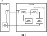
- FIG. 2 is a block diagram of an embodiment of a system having an unmatched receiver circuit that performs error checking on a training signal.
- System 200 includes device 210, which is shown with transmitting hardware TX 212, and device 220, which is shown with receiving hardware 222. It will be understood that in one embodiment device 220 could also send a transmission to device 210; thus device 220 can include transmitting hardware that is not explicitly shown, and device 210 can include receiving hardware that is not explicitly shown.
- the transmitting and receiving hardware is transceiver hardware, which allows interfacing by both transmitting and receiving.
- the devices are connected via one or more transmission lines, which are driven by a transmit driver.
- the transmission line can be any type of signal line (e.g., trace, wire) connecting I/O pins of device 210 with device 220.
- Device 220 includes receive controller 230, which represents hardware and other logic that performs the receiving operations for device 220.
- Receive controller 230 can include sampling circuitry 232 to sample the voltage levels of the received signal from RX 222. Sampling circuitry 232 is controlled by sample strobe 234 or other control signal, which indicates when to sample the incoming or received signal. Sample strobe 234 is generated as a separate signal by receive controller 230.
- Receive controller 230 includes timing control 236 to control the generation of sample strobe 234.
- receive controller 230 includes error checking 238, which includes hardware and/or other logic to determine if errors are detected in a received training signal.
- Drift either positive or negative
- Error checking 238 can determine if the sampling strobe is aligned with the data signal. If a threshold number of errors are received over a number of samples, the system can determine that drift has occurred in the receiver timing. Based on the drift, or the change in delay of the strobe signal or control signal with respect to the data signal, timing control 236 can adjust for the change.
- timing control 236 and/or other control logic adjusts for delay by signaling device 210 to change its transmit parameters to better match the sampling timing of sampling circuitry 232.
- timing control 214 of device 210 can adjust operation of TX 212.
- timing control 236 adjusts the timing of strobe sample 234 to adjust the timing of sampling circuitry 232.
- system 200 controls the timing of the receive circuitry of device 220 with respect to the transmit circuitry of device 210.
- error checking 238 generates an error count that is sent directly to control logic (timing control 214 and/or other logic) of device 210.
- timing control 214 and/or other control logic of device 210 can adjust the operation of device 210 and/or device 220 to compensate for drift.
- timing control 214 and/or timing control 236 could alternatively be labeled as I/O control, indicating that they include logic that adjusts the I/O performance of the devices. The I/O performance adjustment changes the timing of the I/O interface.
- system 200 relates to how to measure tDQS delay (the propagation delay of the data strobe signal), and adjust the controller/processor transmitter timing to compensate for changes in the delay.
- tDQS delay the propagation delay of the data strobe signal
- the I/O interface can be used to exchange a training signal without affecting throughput bandwidth of the I/O interface.
- receive controller 230 employs an unmatched receiver circuit architecture.
- Unmatched architectures are typically sensitive to voltage and temperature changes, so the behavior of the circuit (and specifically the timing) changes over time.
- error checking 2308 allows system 200 to adjust the I/O interface timing, which in turn adjusts the sampling point. Otherwise, the sampling point would drift causing sampling at the wrong part of the signal and result in receive errors.
- the periodic training simply tracks edge movement in the I/O interface, rather than testing the I/O interface performance with respect to worst-case scenario or worst-case pattern.
- the training may not be considered 'robust,' because the training simply determines how much change occurs relative to previously stored values.
- the changes in number of errors detected should indicate movement of the edges of the data signal with respect to the strobe signal.
- the memory device performs the error checking, which allows the testing to be done with fewer reads than writes. For example, the memory device can be configured to ignore or drop a write received during a training mode. Thus, the training can complete much more quickly with respect to having to perform a read for every write as with traditional periodic testing.
- a real read requires a save and a restore, as well as requiring active operation of the memory device, which interferes with real access bandwidth.
- the memory device can simply receive and sample the incoming signal, and then drop it instead of writing it to physical media.
- the memory device can write the incoming signal to a register or register(s) used in training mode for the training signal, and again, not write the data to the physical storage media array. Even in the case where the controller reads the register(s) to detect errors in the training signal, the save and restore is not required.
- the periodic training would preferentially be performed with a sufficient number of training signal samples to allow for averaging the number of errors detected. For example, a spurious condition during a single training signal sample could lead to incorrect results.
- monitoring the number of errors detected, on average, over 100 training signals can produce a more accurate reading of the number of errors. For example, a large number of training signals (e.g., 50 or 100), could be performed during a refresh cycle of the memory device without affecting the overall performance of the memory device.
- PI values or other error tracking values can be stored in a register and monitored with respect to subsequent trainings.
- Control logic can move the data signal edge right or left based on the results of the change in the currently read error tracking value with respect to a previous value.
- the system performs a search, as described below, to determine how to alter performance of the I/O interface to change the data edge.
- system 200 uses the error measurements as input to perform a search that specifically determines settings for the runtime system to improve I/O.
- search logic (which may be part of test logic, or may be separate logic) determines from measured values what settings to use for I/O between the devices.
- the search logic can use the measurements to generate one or more representative performance curves for I/O. Based on the representative curves, the search logic can perform a search function to determine what settings to use to satisfy better performance for at least one parameter, while at least maintaining required (by standard or configuration) performance for the others.
- the search logic can include any of n-dimensional search logic, 1-dimensional search logic (to perform n 1-dimensional searches), linear fit search logic, quadratic fit search logic, steepest descent search logic, curve fitting search logic, or others. It will be understood that n represents an integer indicating the number of combinations to search. In one embodiment, the search logic can also combine multiple measurements together to either reduce repeatability noise or extrapolate to worst case conditions. Thus, control logic can determine to cause an adjustment to a receive I/O parameter of the memory device, and/or a transmit I/O parameter of the controller.
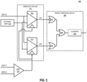
- FIG 3 is a block diagram of an embodiment of a system having an unmatched receiver circuit and error checking circuit that counts errors in a received training signal.
- Circuit 300 provides one example of sampling circuitry and error checking, such as illustrated in system 200 of Figure 2 .
- a memory device of which circuit 300 is a part enters a training mode to perform the training or I/O interface testing.
- the memory device can enter the training mode while an all bank refresh is occurring in the memory device.
- the training can occur approximately every 7.6 uS without consuming I/O bandwidth and impacting performance. It will be understood that training could be performed more frequently, but increased frequency would result in performing training at times other than during refresh, which can negatively impact available I/O bandwidth for memory access operations. It will be understood that performing training at times other than during a refresh can be computed to be during a time of lower load on memory device access, which can reduce the performance effects of the training.
- Circuit 300 is an unmatched receiver circuit, including sampling circuit 310, and unmatched amplifier 330.
- Amplifier 330 is connected to sampling circuit 310 by a clock distribution network, which has been eliminated for purposes of simplicity. However, the difference between the delay through the clock distribution network and the delay of sampling the received data signal DQ[7:0] is what identifies circuit 300 as an unmatched receiver. The change in the delay through the distribution network can cause the drift in the sampling signal as compared to the data signal.
- Sampling circuit 310 samples received data signal DQ[7:0] against an internal reference voltage Vref 320. It will be understood that the data signal can be more of fewer than 8 bits, depending on the configuration of the system in which circuit 300 is a part.
- Sampling circuit 310 includes element 312 to provide a sample of the input signal on the positive sample strobe, and element 314 to provide a sample of the input signal on the complementary portion of the sample strobe. Other configurations are possible.
- Elements 312 and 314 are sampling amplifiers, which sample the actual received signal, and amplify the sample. Thus, the amplification can be performed by a lower speed amplifier as compared to amplifying prior to sampling, as with a matched configuration.
- Amplifier 330 receives as inputs a pull-up strobe signal and a pull-down strobe signal.
- the clock distribution network distributes the strobe or sample signal to multiple different elements, for example, multiple different sampling elements (not shown). The exact number of levels of the distribution network will vary by implementation. Common distribution networks include binary tree (each additional level includes two branches) and H-tree (each additional level includes four branches and looks like an "H") distribution networks.
- the delay from amplifier 330 to sampling elements 312 and 314 changes over time based on operation of the device, through aging, changing voltage levels, changes in temperature, or possibly other operating conditions.
- sampling elements 312 and 314 are fed into error checking circuit 340, a simplified version of which is illustrated in Figure 3 .
- error checking circuit includes inverting gate 342 to receive sample 316 from element 312, sampled at the positive portion of the sample strobe, and noninverting gate 344 to receive sample 318 from element 314, samples at the negative portion of the sample strobe. It will be understood that for a training signal of 1010..., output sample 316 should always be a '1', and output sample 318 should always be a '0'. Thus, the outputs of gates 342 and 344 can be provided as input to XOR gate 346, which should only generate a 1 if there is an error in the received signal. When the received signal is received correctly, gate 346 will always output a zero.
- Counter 350 counts the number of errors detected in the received training signal.
- the sampled incoming training signal is received at error checking circuit 340, but discarded instead of being written to a memory array of the memory device in which circuit 300 is a part.
- counter 350 counts the number of errors detected over a sequence of training signals. Thus, the final count of counter 350 will represent a cumulative value.
- the output of counter 350 is sent to control logic in the memory device, which determines what I/O performance parameters to adjust in response to the number of errors detected. Based on the number of errors detected, the control logic may determine not to adjust any parameters for a particular training sequence.
- the output of counter 350 is sent to control logic in a controller device, which can then determine what I/O performance parameters to adjust in response to the number of errors detected. Either control logic can include search logic to make the determination.
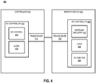
- FIG 4 is a block diagram of an embodiment of a system that adjusts I/O operation based on detection of errors in a training signal sent from a transmitter to a receiver.
- System 400 can be one example of a system in accordance with system 200 of Figure 2 .
- Controller device 410 is the transmitting device
- memory device 420 is the receiving device for purposes of exchange of a training signal or signals to test the I/O interface between the two devices.
- memory device 420 can also communicate back to controller 410, although such communication would not include sending an I/O interface training signal to test the I/O interface.
- Memory device 420 can communicate data back to controller, such as sending a counter value for determination of how to adjust I/O performance parameters, or sending data in response to a read command by the controller (which could include a read of the training signal stored in a training register).
- Controller 410 includes transceiver 412 to interface with memory device 420.
- Memory device 420 includes transceiver 422 to interface with controller 410.
- the connection between the two transceivers is the I/O interface.
- the I/O interface can be understood as including I/O controller 420 of controller 410 and I/O controller 440 of memory device 420.
- I/O controller 420 allows controller 410 to set parameters of transmission and/or reception for transceiver 412.
- I/O controller 440 enables memory device 420 to set parameters of reception and/or transmission for transceiver 422.
- I/O controller 430 includes I/O control 432, which can include registers, tables, and/or other mechanisms that store values associated with I/O via transceiver 412. I/O control 432 controls the settings used by transceiver 412 for physical parameters of communication and/or latency parameters.
- Logic 434 represents control logic at controller device 410, which can enable the controller device to determine what parameter or parameters should be adjusted to compensate for drift as indicated by periodic training.
- I/O controller 440 includes I/O control 446, which can be similar to I/O control 432.
- I/O controller 440 can include registers, tables, and/or other mechanisms that store values associated with I/O via transceiver 422.
- I/O control 446 includes a register or registers used by memory device 420 to temporarily store a training signal for a read by controller device 410, without having to write the signal to the memory array (memory array not shown).
- Logic 444 represents control logic at memory controller 420, which can determine what parameter or parameters to adjust to compensate for drift as indicated by periodic training.
- I/O controller 440 can include sampling circuitry 442 to sample the receive signals.
- sampling circuitry 442 can include error detection circuitry to count a number of errors in a sequence of training samples.
- memory device 420 can be configured to check errors in the training signal.
- controller device 410 can be configured to check errors in the training signal.
- Memory device 420 can check errors by using error checking circuitry. The memory device can then cause an adjustment based on the errors detected and/or indicate the detected errors to controller device 410 to have the controller cause an adjustment based on the errors detected.
- Controller device 410 can check errors by the controller issuing read commands to read back the training data sent.
- An example command test flow could be: Write DataO, Read DataO, Write Data1, Read Data1, ..., where Data0, Data1,... are potentially different data values driven on the bus.
- memory device 420 can be configured to store the training data in a buffer (e.g., a new or existing register or other buffer) between the write and read commands without writing the data to the memory array.
- a buffer e.g., a new or existing register or other buffer
- controller device 410 includes a finite state machine (FSM, not explicitly shown) that controls the periodic training.
- FSM finite state machine
- the FSM can be configured to enable a training mode every N refresh commands, where N is some integer.
- the training could occur every refresh cycle, or less frequently.
- the FSM could alternatively be configured to perform training during a relatively low load time of the memory device after a timer reaches a threshold time.
- the controller device can monitor a known value representing the edge of the data eye, and issue M writes to generate the training signal.
- the error detection can monitor the edge (e.g., the setup timing) as opposed to both setup and hold edges, if only the edge of the data eye is monitored (as opposed to the whole eye).
- the controller device can read back the error count and/or read back the written data, and determine if the data edge should be incremented or decremented.
- the FSM can move the data eye edge one or more ticks (or subdivided portions, as done with phase interpolation). The FSM can run the test to determine which direction to move the edge of the eye.
- control logic of controller device 410 (if the controller device causes error adjustments) or control logic of memory device 420 (if the memory device causes error adjustments) can offset settings associated with the center of the data eye, in response to changes detected in the edge of the eye.
- the periodic training can monitor an edge of the eye, and move a center of the eye commensurate with a change or movement detected in the edge of the eye.
- the centering of the eye could be done on a channel, word, byte, or bit basis as required. It will be understood that the amount of the feedback from the memory device to the controller device may need to be increased depending on how the centering is performed.
- memory device 420 includes multiple ranks.
- error detection can be performed on a rank by rank basis.
- error detection can be performed on a selected rank, and applied across all ranks. Specific implementation details will be based on environmental constraints such as how much difference in temperature or voltage is expected to exist across different ranks.
- the periodic training can be understood as a digital feedback loop.
- Digital feedback loops typically dither between two adjacent settings.
- the value of a PI edge setting can dither between two adjacent settings, but the dithering can be filtered out of a PI center setting using known digital filtering techniques.
- the PI center setting could move only after the PI edge setting moves twice in the same direction (e.g., the center PI always lags the edge movement by one setting).
- a filter can eliminate the feedback dithering as a source of noise.
- the control logic that determines how to adjust I/O parameter setting(s) to compensate for drift can collect more or less data, and/or search more settings or parameters.
- the logic can make the tradeoff between more of less data, and more search time or less search time based on prior drift results, power state activity, temperature changes, and/or other environmental changes in the system. For example, frequent fluctuation in temperature/voltage, or high variance in prior drift results can indicate that more settings can be used, and/or that a results search can used more processing to achieve a more accurate result. Very little variance can indicate the opposite.
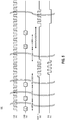
- FIG. 5 is a timing diagram of an embodiment of operation timing for detecting errors in a received training signal.
- Timing diagram 500 illustrates one embodiment of a flow of commands to a DRAM device, which can be one example of a memory device in accordance with any embodiment described.
- Clock signal 510 is the system clock.
- CMD 520 is the DRAM command signal sent by a memory controller, which can be one example of a controller device in accordance with any embodiment described.
- PRE ALL represents an initial state of the system for purposes of the training. There is a delay of tRPab between PRE ALL and the issuance of the MRW Entry command.
- MRW (mode register write) Entry represents a command to enter a special training state.
- the training state is a special mode that can be enabled using an MRW, an explicit command, or some similar mechanism.
- the host or memory controller can issue normal Write command(s) to the DRAM.
- the write command and MRW are the same command.
- the DRAM treats the writes differently when received in the training state versus when writes are received not in the training state. For example, the DRAM can check that the write data matches the desired training pattern without accessing the internal memory array.
- DRAM error checking is very simple when a training pattern of 1010 is used. For example, with a 1010 training pattern, the checking logic can require that all rising DQS samples be 1 and all falling DQS samples be 0. The DRAM can check if any lane in a byte experienced an error for each cycle. In one embodiment, if one or more errors are detected in a given cycle, the DRAM increments an error counter by one. In one embodiment, each DQ byte has a separate N-bit counter in the DRAM to count errors. The count of the counter can provide a much more accurate view of the average relative positions of DQS as compared to DQ, which allows control logic to filter noise from a few bad samples, reducing noise and training time.
- DRAM combines error counts from different lanes and DQS edges before the counter, which makes sure that the training focuses on the worst case lane/edge.
- the memory controller can issue a MRR command or similar command to read the error results.
- an MRR result command is issued to the DRAM.
- the memory controller can issue an MRW exit command, and/or the memory device can exit the training state.
- the memory controller reads the error counter results.
- the error count can be automatically reset to 0 by the MRW training mode enter command.
- the memory controller could also reissue a MRW training mode command, even if the DRAM is already in the training state or training mode, for the purposes of resetting the counter.
- Figure 6A is a flow diagram of an embodiment of a process for checking for errors in a received training signal, with error checking performed by the receiving device.
- a memory device enters a refresh mode, 602.
- a memory controller can send a command to the memory device to cause the memory device to enter the refresh mode.
- the memory device typically cannot receive and process commands from the memory controller, because access to the memory array is not permitted.
- a memory controller can send a command at a time other than during refresh.
- the memory controller sends a training mode indicator to the memory device, 604.
- the training mode indicator could be a command sent by the memory controller.
- the training mode indicator could be a register setting of the memory device that the memory controller sets.
- the memory device enters the training mode, 606.
- the memory device can receive certain training commands over the command bus, and process the commands, while not accessing the memory array.
- the memory controller can send I/O for processing by the memory controller.
- the training I/O is normal I/O from the perspective of the I/O interface. However, from the perspective of access to the memory array, the training I/O is a "dummy" I/O, meaning the I/O does not generate an access to the memory array.
- a training signal or sequence of training signals is sent from the memory controller to the memory device, 610.
- the memory controller sends the training signal as a training mode write.
- the training mode write can be a normal write command send while the memory device is in the training mode, or can be a write command specific to training.
- the memory device receives the training mode write, 612.
- the memory device treats the training mode writes differently than typical write commands in that the memory device receive processor does not forward the data for access to the memory array media.
- the memory device evaluates the training signal for errors, and increments an error count when an error is detected, 614.
- control logic determines whether and/or how to adjust one or more I/O parameters based on the final error count, 618.
- the control logic uses a search function to evaluate I/O parameters.
- the control logic is part of the memory device.
- the control logic is part of the memory controller.
- the control logic determines to adjust an I/O parameter related to transmission by the memory controller.
- the control logic determines to adjust an I/O parameter related to receiving the signal by the memory device. The system adjusts the determined I/O parameter(s) in accordance with the determination, 620.
- Figure 6B is a flow diagram of an embodiment of a process for checking for errors in a received training signal, with error checking performed by the transmitting device. It will be observed that Figure 6B differs from Figure 6A at 630, 632, and 634. Otherwise, the flow of operations is similar or the same as what is stated above. Rather than repeating what is stated above, the description of Figure 6B will focus on the portions that are different.
- the memory controller evaluates the training signal for error as follows.
- the memory device receives the training mode write, 612, and the memory device writes the training signal to a training buffer, but the memory device does not write to the memory array, 630.
- the memory controller reads the training signal from the training buffer in a subsequent operation, 632.
- the memory controller can issue a training buffer read command.
- the training buffer can be an existing register or buffer of the memory device, which the memory controller can access through a register read command, for example.
- the memory controller evaluates the read signal for errors, and increments an error count when an error is detected, 634. Again, the process continues for all I/O to be sent by the memory controller to the memory device for the training sequence.
- control logic at the memory controller or at the memory device determines whether and/or how to adjust one or more I/O parameters based on the error count.
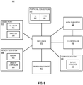
- FIG. 7 is a block diagram of an embodiment of a computing system in which receive signal error checking can be implemented.
- System 700 represents a computing device in accordance with any embodiment described herein, and can be a laptop computer, a desktop computer, a server, a gaming or entertainment control system, a scanner, copier, printer, routing or switching device, or other electronic device.
- System 700 includes processor 720, which provides processing, operation management, and execution of instructions for system 700.
- Processor 720 can include any type of microprocessor, central processing unit (CPU), processing core, or other processing hardware to provide processing for system 700.
- Processor 720 controls the overall operation of system 700, and can be or include, one or more programmable general-purpose or special-purpose microprocessors, digital signal processors (DSPs), programmable controllers, application specific integrated circuits (ASICs), programmable logic devices (PLDs), or the like, or a combination of such devices.
- DSPs digital signal processors
- ASICs application specific integrated circuits
- PLDs programmable logic devices
- Memory subsystem 730 represents the main memory of system 700, and provides temporary storage for code to be executed by processor 720, or data values to be used in executing a routine.
- Memory subsystem 730 can include one or more memory devices such as read-only memory (ROM), flash memory, one or more varieties of random access memory (RAM), or other memory devices, or a combination of such devices.
- Memory subsystem 730 stores and hosts, among other things, operating system (OS) 736 to provide a software platform for execution of instructions in system 700. Additionally, other instructions 738 are stored and executed from memory subsystem 730 to provide the logic and the processing of system 700. OS 736 and instructions 738 are executed by processor 720.
- OS operating system
- Memory subsystem 730 includes memory device 732 where it stores data, instructions, programs, or other items.
- memory subsystem includes memory controller 734, which is a memory controller in accordance with any embodiment described herein, and which includes a scheduler to generate and issue commands to memory device 732.
- memory subsystem 730 and memory device 732 implement I/O timing compensation based on feedback generated via periodic training.
- Memory device 732 enters a training state, and memory controller 734 sends a training signal via the I/O interface between the memory device and the memory controller, which the memory device does not store in its memory array.
- memory device 732 evaluates the received training signal for errors.
- memory device 732 stores the training signal in a training buffer, which can be any buffer used to store the training signal, and memory controller 734 reads the buffered training signal, and evaluates the signal for errors. Based on detected errors, the system adjusts one or more I/O parameters of either the memory controller or the memory device or both to compensate for changes in environmental conditions that affect I/O timing.
- Bus 710 is an abstraction that represents any one or more separate physical buses, communication lines/interfaces, and/or point-to-point connections, connected by appropriate bridges, adapters, and/or controllers. Therefore, bus 710 can include, for example, one or more of a system bus, a Peripheral Component Interconnect (PCI) bus, a HyperTransport or industry standard architecture (ISA) bus, a small computer system interface (SCSI) bus, a universal serial bus (USB), or an Institute of Electrical and Electronics Engineers (IEEE) standard 1394 bus (commonly referred to as "Firewire").
- PCI Peripheral Component Interconnect
- ISA HyperTransport or industry standard architecture
- SCSI small computer system interface
- USB universal serial bus
- IEEE Institute of Electrical and Electronics Engineers
- the buses of bus 710 can also correspond to interfaces in network interface 750.
- System 700 also includes one or more input/output (I/O) interface(s) 740, network interface 750, one or more internal mass storage device(s) 760, and peripheral interface 770 coupled to bus 710.
- I/O interface 740 can include one or more interface components through which a user interacts with system 700 (e.g., video, audio, and/or alphanumeric interfacing).
- Network interface 750 provides system 700 the ability to communicate with remote devices (e.g., servers, other computing devices) over one or more networks.
- Network interface 750 can include an Ethernet adapter, wireless interconnection components, USB (universal serial bus), or other wired or wireless standards-based or proprietary interfaces.
- Storage 760 can be or include any conventional medium for storing large amounts of data in a nonvolatile manner, such as one or more magnetic, solid state, or optical based disks, or a combination.
- Storage 760 holds code or instructions and data 762 in a persistent state (i.e., the value is retained despite interruption of power to system 700).
- Storage 760 can be generically considered to be a "memory," although memory 730 is the executing or operating memory to provide instructions to processor 720. Whereas storage 760 is nonvolatile, memory 730 can include volatile memory (i.e., the value or state of the data is indeterminate if power is interrupted to system 700).
- Peripheral interface 770 can include any hardware interface not specifically mentioned above. Peripherals refer generally to devices that connect dependently to system 700. A dependent connection is one where system 700 provides the software and/or hardware platform on which operation executes, and with which a user interacts.
- FIG. 8 is a block diagram of an embodiment of a mobile device in which receive signal error checking can be implemented.
- Device 800 represents a mobile computing device, such as a computing tablet, a mobile phone or smartphone, a wireless-enabled e-reader, or other mobile device. It will be understood that certain of the components are shown generally, and not all components of such a device are shown in device 800.
- Device 800 includes processor 810, which performs the primary processing operations of device 800.
- Processor 810 can include one or more physical devices, such as microprocessors, application processors, microcontrollers, programmable logic devices, or other processing means.
- processor 810 includes optical interface components in addition to a processor die.
- the processor die and photonic components are in the same package.
- Such a processor package can interface optically with an optical connector in accordance with any embodiment described herein.
- the processing operations performed by processor 810 include the execution of an operating platform or operating system on which applications and/or device functions are executed.
- the processing operations include operations related to I/O (input/output) with a human user or with other devices, operations related to power management, and/or operations related to connecting device 800 to another device.
- the processing operations can also include operations related to audio I/O and/or display I/O.
- device 800 includes audio subsystem 820, which represents hardware (e.g., audio hardware and audio circuits) and software (e.g., drivers, codecs) components associated with providing audio functions to the computing device. Audio functions can include speaker and/or headphone output, as well as microphone input. Devices for such functions can be integrated into device 800, or connected to device 800. In one embodiment, a user interacts with device 800 by providing audio commands that are received and processed by processor 810.
- hardware e.g., audio hardware and audio circuits
- software e.g., drivers, codecs
- Display subsystem 830 represents hardware (e.g., display devices) and software (e.g., drivers) components that provide a visual and/or tactile display for a user to interact with the computing device.
- Display subsystem 830 includes display interface 832, which includes the particular screen or hardware device used to provide a display to a user.
- display interface 832 includes logic separate from processor 810 to perform at least some processing related to the display.
- display subsystem 830 includes a touchscreen device that provides both output and input to a user.
- I/O controller 840 represents hardware devices and software components related to interaction with a user. I/O controller 840 can operate to manage hardware that is part of audio subsystem 820 and/or display subsystem 830. Additionally, I/O controller 840 illustrates a connection point for additional devices that connect to device 800 through which a user might interact with the system. For example, devices that can be attached to device 800 might include microphone devices, speaker or stereo systems, video systems or other display device, keyboard or keypad devices, or other I/O devices for use with specific applications such as card readers or other devices.
- I/O controller 840 can interact with audio subsystem 820 and/or display subsystem 830.
- input through a microphone or other audio device can provide input or commands for one or more applications or functions of device 800.
- audio output can be provided instead of or in addition to display output.
- display subsystem includes a touchscreen
- the display device also acts as an input device, which can be at least partially managed by I/O controller 840.
- I/O controller 840 manages devices such as accelerometers, cameras, light sensors or other environmental sensors, gyroscopes, global positioning system (GPS), or other hardware that can be included in device 800.
- the input can be part of direct user interaction, as well as providing environmental input to the system to influence its operations (such as filtering for noise, adjusting displays for brightness detection, applying a flash for a camera, or other features).
- device 800 includes power management 850 that manages battery power usage, charging of the battery, and features related to power saving operation.
- Memory subsystem 860 includes memory device(s) 862 for storing information in device 800.
- Memory subsystem 860 can include nonvolatile (state does not change if power to the memory device is interrupted) and/or volatile (state is indeterminate if power to the memory device is interrupted) memory devices.
- Memory 860 can store application data, user data, music, photos, documents, or other data, as well as system data (whether long-term or temporary) related to the execution of the applications and functions of system 800.
- memory subsystem 860 includes memory controller 864 (which could also be considered part of the control of system 800, and could potentially be considered part of processor 810).
- Memory controller 864 includes a scheduler to generate and issue commands to memory device 862.
- memory subsystem 860 and memory device 862 implement I/O timing compensation based on feedback generated via periodic training.
- Memory device 862 enters a training state, and memory controller 864 sends a training signal via the I/O interface between the memory device and the memory controller, which the memory device does not store in its memory array.
- memory device 862 evaluates the received training signal for errors.
- memory device 862 stores the training signal in a training buffer, which can be any buffer used to store the training signal, and memory controller 864 reads the buffered training signal, and evaluates the signal for errors. Based on detected errors, the system adjusts one or more I/O parameters of either the memory controller or the memory device or both to compensate for changes in environmental conditions that affect I/O timing.
- Connectivity 870 includes hardware devices (e.g., wireless and/or wired connectors and communication hardware) and software components (e.g., drivers, protocol stacks) to enable device 800 to communicate with external devices.
- the device could be separate devices, such as other computing devices, wireless access points or base stations, as well as peripherals such as headsets, printers, or other devices.
- Connectivity 870 can include multiple different types of connectivity.
- device 800 is illustrated with cellular connectivity 872 and wireless connectivity 874.
- Cellular connectivity 872 refers generally to cellular network connectivity provided by wireless carriers, such as provided via GSM (global system for mobile communications) or variations or derivatives, CDMA (code division multiple access) or variations or derivatives, TDM (time division multiplexing) or variations or derivatives, LTE (long term evolution - also referred to as "4G”), or other cellular service standards.
- Wireless connectivity 874 refers to wireless connectivity that is not cellular, and can include personal area networks (such as Bluetooth), local area networks (such as WiFi), and/or wide area networks (such as WiMax), or other wireless communication.
- Wireless communication refers to transfer of data through the use of modulated electromagnetic radiation through a non-solid medium. Wired communication occurs through a solid communication medium.
- Peripheral connections 880 include hardware interfaces and connectors, as well as software components (e.g., drivers, protocol stacks) to make peripheral connections. It will be understood that device 800 could both be a peripheral device ("to” 882) to other computing devices, as well as have peripheral devices ("from” 884) connected to it. Device 800 commonly has a "docking" connector to connect to other computing devices for purposes such as managing (e.g., downloading and/or uploading, changing, synchronizing) content on device 800. Additionally, a docking connector can allow device 800 to connect to certain peripherals that allow device 800 to control content output, for example, to audiovisual or other systems.
- software components e.g., drivers, protocol stacks
- device 800 can make peripheral connections 880 via common or standards-based connectors.
- Common types can include a Universal Serial Bus (USB) connector (which can include any of a number of different hardware interfaces), DisplayPort including MiniDisplayPort (MDP), High Definition Multimedia Interface (HDMI), Firewire, or other type.
- USB Universal Serial Bus
- MDP MiniDisplayPort
- HDMI High Definition Multimedia Interface
- Firewire or other type.
- the content can be directly executable ("object” or “executable” form), source code, or difference code (“delta” or “patch” code).
- the software content of the embodiments described herein can be provided via an article of manufacture with the content stored thereon, or via a method of operating a communication interface to send data via the communication interface.
- a machine readable storage medium can cause a machine to perform the functions or operations described, and includes any mechanism that stores information in a form accessible by a machine (e.g., computing device, electronic system, etc.), such as recordable/non-recordable media (e.g., read only memory (ROM), random access memory (RAM), magnetic disk storage media, optical storage media, flash memory devices, etc.).
- a communication interface includes any mechanism that interfaces to any of a hardwired, wireless, optical, etc., medium to communicate to another device, such as a memory bus interface, a processor bus interface, an Internet connection, a disk controller, etc.
- the communication interface can be configured by providing configuration parameters and/or sending signals to prepare the communication interface to provide a data signal describing the software content.
- the communication interface can be accessed via one or more commands or signals sent to the communication interface.
- Each component described herein can be a means for performing the operations or functions described.
- Each component described herein includes software, hardware, or a combination of these.
- the components can be implemented as software modules, hardware modules, special-purpose hardware (e.g., application specific hardware, application specific integrated circuits (ASICs), digital signal processors (DSPs), etc.), embedded controllers, hardwired circuitry, etc.
- special-purpose hardware e.g., application specific hardware, application specific integrated circuits (ASICs), digital signal processors (DSPs), etc.
- embedded controllers e.g., hardwired circuitry, etc.
Landscapes
- Engineering & Computer Science (AREA)
- Software Systems (AREA)
- Theoretical Computer Science (AREA)
- General Physics & Mathematics (AREA)
- Physics & Mathematics (AREA)
- Evolutionary Computation (AREA)
- Medical Informatics (AREA)
- Computer Vision & Pattern Recognition (AREA)
- Artificial Intelligence (AREA)
- General Engineering & Computer Science (AREA)
- Data Mining & Analysis (AREA)
- Computing Systems (AREA)
- Mathematical Physics (AREA)
- Health & Medical Sciences (AREA)
- Automation & Control Theory (AREA)
- Techniques For Improving Reliability Of Storages (AREA)
- Dram (AREA)
- Memory System (AREA)
Claims (8)
- Verfahren zum Trainieren von Eingabe/Ausgabe-Einstellungen, E/A-Einstellungen, zur Kommunikation mit einer Speichervorrichtung (220), umfassend:Wechseln, durch eine Speichervorrichtung, in einen Trainingsmodus der Speichervorrichtung;Empfangen, durch die Speichervorrichtung, eines Trainingssignals von einer Steuerung (230), während sie sich im Trainingsmodus befindet, das Trainingssignal einschließlich eines Datenstroms;Abtasten, durch die Speichervorrichtung, des Datenstroms des Trainingssignals mit Abtastschaltungen (232) ;Nachverfolgen, durch die Speichervorrichtung, einer Anzahl von Datenfehlern beim Abtasten des Datenstroms des Trainingssignals;Zählen, durch die Speichervorrichtung, mit einem Zähler, einer Anzahl von Fehlern, die über eine Folge von Trainingssignalen auftreten;Senden, durch die Speichervorrichtung, der Anzahl von Fehlern an die Steuerung undBewirken, durch die Steuerung, einer Einstellung an zumindest einem Eingabe/Ausgabe-Parameter, E/A-Parameter, der Steuerung und/oder der Speichervorrichtung, wenn eine Schwellenanzahl von Datenfehlern empfangen wird.
- Verfahren nach Anspruch 1, wobei das Wechseln in den Trainingsmodus ein Wechseln in den Trainingsmodus während eines Aktualisierungsmodus der Speichervorrichtung umfasst.
- Verfahren nach Anspruch 1 oder 2, wobei das Empfangen des Trainingssignals umfasst:Empfangen des Trainingssignals als einen Schreibbefehl undVerwerfen des Trainingssignals, anstatt dieses in ein Speicher-Array der Speichervorrichtung zu schreiben.
- Verfahren nach einem der Ansprüche 1 bis 3, wobei das Bewirken der Einstellung umfasst:
Bewirken der Einstellung an einem Empfangs-E/A-Parameter der Speichervorrichtung. - Verfahren nach einem der Ansprüche 1 bis 3, wobei das Bewirken der Einstellung umfasst:
Bewirken der Einstellung an einem Übertragungs-E/A-Parameter der Steuerung. - Verfahren nach einem der Ansprüche 1 bis 5, wobei das Bewirken der Einstellung ferner umfasst:
Berechnen einer Suchfunktion zum Bestimmen des zumindest einen einzustellenden E/A-Parameters. - System, umfassend ein Mittel zum Durchführen von Vorgängen zum Ausführen eines Verfahrens nach einem der Ansprüche 1 bis 6.
- Verfahren nach Anspruch 1, ferner umfassend:
Senden des Trainingssignals als einen Schreibbefehl an die Speichervorrichtung, wobei die Speichervorrichtung das Trainingssignal in ein Register, aber nicht in ein Speicher-Array der Speichervorrichtung schreibt.
Applications Claiming Priority (2)
| Application Number | Priority Date | Filing Date | Title |
|---|---|---|---|
| US14/018,217 US9218575B2 (en) | 2013-09-04 | 2013-09-04 | Periodic training for unmatched signal receiver |
| PCT/US2014/052492 WO2015034701A1 (en) | 2013-09-04 | 2014-08-25 | Periodic training for unmatched signal receiver |
Publications (3)
| Publication Number | Publication Date |
|---|---|
| EP3042293A1 EP3042293A1 (de) | 2016-07-13 |
| EP3042293A4 EP3042293A4 (de) | 2017-04-19 |
| EP3042293B1 true EP3042293B1 (de) | 2021-07-21 |
Family
ID=52584652
Family Applications (1)
| Application Number | Title | Priority Date | Filing Date |
|---|---|---|---|
| EP14843012.7A Active EP3042293B1 (de) | 2013-09-04 | 2014-08-25 | Periodisches training für empfänger ungleicher signale |
Country Status (6)
| Country | Link |
|---|---|
| US (1) | US9218575B2 (de) |
| EP (1) | EP3042293B1 (de) |
| JP (1) | JP6274683B2 (de) |
| KR (1) | KR102024682B1 (de) |
| CN (1) | CN105706069B (de) |
| WO (1) | WO2015034701A1 (de) |
Families Citing this family (38)
| Publication number | Priority date | Publication date | Assignee | Title |
|---|---|---|---|---|
| US9287003B2 (en) * | 2013-12-06 | 2016-03-15 | Rambus Inc. | Multi-cycle write leveling |
| US9348705B1 (en) * | 2014-06-26 | 2016-05-24 | Inphi Corporation | Memory controller system with non-volatile backup storage |
| US9535119B2 (en) | 2014-06-30 | 2017-01-03 | Intel Corporation | Duty cycle based timing margining for I/O AC timing |
| US9921899B2 (en) * | 2014-12-18 | 2018-03-20 | Oracle International Corporation | Monitoring serial link errors |
| US9886987B1 (en) * | 2014-12-30 | 2018-02-06 | Cadence Design System, Inc. | System and method for data-mask training in non-provisioned random access memory |
| KR102461460B1 (ko) * | 2015-06-08 | 2022-11-02 | 삼성전자주식회사 | 비휘발성 메모리 모듈, 그것을 포함하는 컴퓨팅 시스템 및 그것의 pvt 보상 방법 |
| US10261697B2 (en) * | 2015-06-08 | 2019-04-16 | Samsung Electronics Co., Ltd. | Storage device and operating method of storage device |
| US9715907B1 (en) * | 2016-05-09 | 2017-07-25 | Invecas, Inc. | Optimal data eye for improved Vref margin |
| US10103837B2 (en) * | 2016-06-23 | 2018-10-16 | Advanced Micro Devices, Inc. | Asynchronous feedback training |
| KR20180005081A (ko) | 2016-07-05 | 2018-01-15 | 삼성전자주식회사 | 커맨드 윈도우 발생부를 갖는 메모리 장치 |
| US10115480B1 (en) * | 2017-07-03 | 2018-10-30 | Qualcomm Incorporated | Double data rate synchronous dynamic random access memory (“DDR SDRAM”) data strobe signal calibration |
| KR102392055B1 (ko) * | 2017-08-09 | 2022-04-28 | 삼성전자주식회사 | 리트레이닝 동작의 수행 여부를 효율적으로 결정하기 위한 메모리 장치 및 이를 포함하는 메모리 시스템 |
| US11604714B2 (en) | 2017-08-09 | 2023-03-14 | Samsung Electronics Co, Ltd. | Memory device for efficiently determining whether to perform re-training operation and memory system including the same |
| US10572183B2 (en) * | 2017-10-18 | 2020-02-25 | Advanced Micro Devices, Inc. | Power efficient retraining of memory accesses |
| KR102407439B1 (ko) * | 2017-12-05 | 2022-06-10 | 삼성전자주식회사 | 메모리 장치의 구동 강도, odt 트레이닝 방법, 이를 수행하는 컴퓨팅 시스템 및 시스템 온 칩 |
| KR102401182B1 (ko) | 2018-01-19 | 2022-05-24 | 삼성전자주식회사 | 메모리 장치 및 메모리 패키지 |
| KR102499794B1 (ko) * | 2018-05-21 | 2023-02-15 | 삼성전자주식회사 | 스토리지 장치 및 스토리지 장치의 동작 방법 |
| US10573272B2 (en) | 2018-06-28 | 2020-02-25 | Intel Corporation | Device, method and system for providing a delayed clock signal to a circuit for latching data |
| KR102674619B1 (ko) * | 2018-07-11 | 2024-06-13 | 에스케이하이닉스 주식회사 | 메모리 시스템 및 메모리 시스템의 동작 방법 |
| JP2020047340A (ja) * | 2018-09-19 | 2020-03-26 | キオクシア株式会社 | 不揮発性メモリ及びメモリシステム |
| DE102018216078A1 (de) * | 2018-09-20 | 2020-03-26 | Robert Bosch Gmbh | Verfahren und Vorrichtung zum Betreiben eines Steuerungssystems |
| KR102691395B1 (ko) * | 2018-12-20 | 2024-08-05 | 에스케이하이닉스 주식회사 | 메모리 시스템, 메모리 시스템의 동작 방법 및 메모리 콘트롤러 |
| KR102685470B1 (ko) * | 2018-12-24 | 2024-07-17 | 에스케이하이닉스 주식회사 | 트래이닝 기능을 갖는 반도체 장치 및 반도체 시스템 |
| US11449439B1 (en) | 2019-07-25 | 2022-09-20 | Rambus Inc. | Fragmented periodic timing calibration |
| KR102772896B1 (ko) * | 2019-09-19 | 2025-02-27 | 에스케이하이닉스 주식회사 | 메모리 장치 및 그 동작 방법 |
| KR102849290B1 (ko) | 2020-08-21 | 2025-08-25 | 삼성전자주식회사 | 반도체 장치 및 메모리 시스템 |
| KR102843218B1 (ko) | 2021-02-25 | 2025-08-06 | 삼성전자주식회사 | 메모리 장치의 dq 캘리브레이션 패턴의 최적화 방법 및 이를 수행하는 컴퓨팅 시스템 |
| US11740966B2 (en) * | 2021-04-19 | 2023-08-29 | Samsung Electronics Co., Ltd. | Memory device and operating method of the memory device and host device |
| KR102855161B1 (ko) * | 2021-11-04 | 2025-09-03 | 삼성전자주식회사 | 메모리 장치, 호스트 장치 및 메모리 장치의 구동 방법 |
| CN114496047B (zh) * | 2021-12-29 | 2023-08-29 | 深圳市紫光同创电子有限公司 | 双向数据选通采样信号dqs相位的调整方法及装置 |
| CN115113686B (zh) * | 2022-04-25 | 2025-11-18 | 腾讯科技(深圳)有限公司 | 时序调整方法和装置、存储介质及电子设备 |
| US12334186B2 (en) | 2022-06-10 | 2025-06-17 | Samsung Electronics Co., Ltd. | Memory device, memory system and method for operating memory system including command and address training |
| US20220358061A1 (en) * | 2022-07-25 | 2022-11-10 | Intel Corporation | Unmatched architecture compensation via digital component delay |
| KR20240020596A (ko) * | 2022-08-08 | 2024-02-15 | 삼성전자주식회사 | 입출력 호환성을 제공하는 불휘발성 메모리 장치 및 그것의 호환성 설정 방법 |
| US12619562B2 (en) | 2022-08-18 | 2026-05-05 | Intel Corporation | Unidirectional command bus phase drift compensation by sending the command bus delay to memory controller |
| CN120112896A (zh) * | 2023-08-24 | 2025-06-06 | 长江存储科技有限责任公司 | 一种存储控制器的操作方法、存储控制器及存储系统 |
| US12548609B2 (en) | 2024-01-29 | 2026-02-10 | SanDisk Technologies, Inc. | Feed-forward data toggling based delay circuit |
| US20240345969A1 (en) * | 2024-06-26 | 2024-10-17 | Intel Corporation | Dynamically insert timing and voltage offset control (voc) offsets in input/output (io) during functional traffic |
Citations (2)
| Publication number | Priority date | Publication date | Assignee | Title |
|---|---|---|---|---|
| WO2009134844A1 (en) * | 2008-05-02 | 2009-11-05 | Rambus Inc. | High-speed source-synchronous signaling |
| US20130055039A1 (en) * | 2011-08-30 | 2013-02-28 | Glenn A. Dearth | Fully Programmable Parallel PRBS Generator |
Family Cites Families (47)
| Publication number | Priority date | Publication date | Assignee | Title |
|---|---|---|---|---|
| KR100383404B1 (ko) * | 1996-08-16 | 2003-07-16 | 동경 엘렉트론 디바이스 주식회사 | 반도체메모리장치및반도체메모리장치에있어서의데이타기입/판독방법 |
| WO1999046775A2 (en) * | 1998-03-10 | 1999-09-16 | Rambus, Inc. | Performing concurrent refresh and current control operations in a memory subsystem |
| JP3090138B2 (ja) * | 1999-02-04 | 2000-09-18 | 日本電気株式会社 | 受信機 |
| US6493836B2 (en) * | 2000-11-30 | 2002-12-10 | Compaq Information Technologies Group, L.P. | Method and apparatus for scheduling and using memory calibrations to reduce memory errors in high speed memory devices |
| US6847617B2 (en) | 2001-03-26 | 2005-01-25 | Intel Corporation | Systems for interchip communication |
| US6522174B2 (en) | 2001-04-16 | 2003-02-18 | Intel Corporation | Differential cascode current mode driver |
| US7155006B2 (en) | 2001-09-21 | 2006-12-26 | Intel Corporation | Method and apparatus for outbound wave subtraction using a variable offset amplifier |
| US6894536B2 (en) | 2001-12-10 | 2005-05-17 | Intel Corporation | Low power NRZ interconnect for pulsed signaling |
| US7259606B2 (en) | 2004-01-27 | 2007-08-21 | Nvidia Corporation | Data sampling clock edge placement training for high speed GPU-memory interface |
| US7246274B2 (en) | 2004-09-10 | 2007-07-17 | Rambus Inc. | Method and apparatus for estimating random jitter (RJ) and deterministic jitter (DJ) from bit error rate (BER) |
| US7630489B2 (en) * | 2004-09-16 | 2009-12-08 | Infineon Technologies Ag | Adaptive communication systems and methods |
| US20070245177A1 (en) * | 2006-03-24 | 2007-10-18 | General Instrument Corporation | Method and apparatus for determining the total power margin available for an hfc network |
| US7647467B1 (en) | 2006-05-25 | 2010-01-12 | Nvidia Corporation | Tuning DRAM I/O parameters on the fly |
| US7602056B2 (en) | 2006-06-14 | 2009-10-13 | Intel Corporation | On-die termination method for multi-chip packages |
| KR101206503B1 (ko) * | 2006-06-30 | 2012-11-29 | 삼성전자주식회사 | 스큐 제거 회로 및 그에 의한 스큐 제거 방법 |
| US7694031B2 (en) * | 2006-10-31 | 2010-04-06 | Globalfoundries Inc. | Memory controller including a dual-mode memory interconnect |
| KR100862341B1 (ko) | 2006-11-13 | 2008-10-13 | 삼성전기주식회사 | 사람의 피부 영역 검출장치 및 그 방법 |
| KR20080044543A (ko) * | 2006-11-16 | 2008-05-21 | 삼성전자주식회사 | 병렬 인터페이스를 이용하는 메모리 장치의 스큐를보상하는 방법 |
| US7624225B2 (en) * | 2007-03-22 | 2009-11-24 | International Business Machines Corporation | System and method for providing synchronous dynamic random access memory (SDRAM) mode register shadowing in a memory system |
| US7886174B2 (en) | 2007-06-27 | 2011-02-08 | Intel Corporation | Memory link training |
| US7979039B2 (en) | 2007-09-24 | 2011-07-12 | Intel Corporation | Pre-distorting a transmitted signal for offset cancellation |
| US7622946B2 (en) | 2007-11-05 | 2009-11-24 | International Business Machines Corporation | Design structure for an automatic driver/transmission line/receiver impedance matching circuitry |
| US7924637B2 (en) | 2008-03-31 | 2011-04-12 | Advanced Micro Devices, Inc. | Method for training dynamic random access memory (DRAM) controller timing delays |
| JP5248677B2 (ja) * | 2008-07-01 | 2013-07-31 | イカノス テクノロジー リミテッド | メモリ削減されたベクトル化されたdsl |
| JP2010026651A (ja) * | 2008-07-16 | 2010-02-04 | Toshiba Storage Device Corp | シリアルインターフェース回路の自動調整方法及びシリアルインターフェース回路を備えた電子装置 |
| US8008944B2 (en) | 2008-11-25 | 2011-08-30 | Qualcomm Incorporated | Low voltage differential signaling driver with programmable on-chip resistor termination |
| JPWO2010100685A1 (ja) * | 2009-03-03 | 2012-09-06 | パナソニック株式会社 | メモリ装置およびメモリ制御装置 |
| US7898295B1 (en) | 2009-03-19 | 2011-03-01 | Pmc-Sierra, Inc. | Hot-pluggable differential signaling driver |
| US8819474B2 (en) | 2009-04-03 | 2014-08-26 | Intel Corporation | Active training of memory command timing |
| US20120151300A1 (en) * | 2009-08-25 | 2012-06-14 | Tillema John E | Error Correcting |
| US8331176B2 (en) | 2009-11-30 | 2012-12-11 | Intel Corporation | Method and system for evaluating effects of signal phase difference on a memory system |
| US8582374B2 (en) | 2009-12-15 | 2013-11-12 | Intel Corporation | Method and apparatus for dynamically adjusting voltage reference to optimize an I/O system |
| US8868992B2 (en) | 2009-12-31 | 2014-10-21 | Intel Corporation | Robust memory link testing using memory controller |
| US8681571B2 (en) | 2010-06-15 | 2014-03-25 | International Business Machines Corporation | Training a memory controller and a memory device using multiple read and write operations |
| KR101791456B1 (ko) | 2010-10-11 | 2017-11-21 | 삼성전자주식회사 | 라이트 트레이닝 방법 및 이를 수행하는 반도체 장치 |
| US9830954B2 (en) | 2011-03-23 | 2017-11-28 | Intel Corporation | Method and system for dynamic power management of memories |
| WO2012145117A2 (en) * | 2011-04-22 | 2012-10-26 | Rambus Inc. | Memory components and controllers that calibrate multiphase synchronous timing references |
| US20120284576A1 (en) * | 2011-05-06 | 2012-11-08 | Housty Oswin E | Hardware stimulus engine for memory receive and transmit signals |
| US8934311B2 (en) * | 2011-09-06 | 2015-01-13 | Samsung Electronics Co., Ltd. | Semiconductor memory device capable of screening a weak bit and repairing the same |
| KR101599656B1 (ko) | 2011-12-22 | 2016-03-03 | 인텔 코포레이션 | 온-패키지 입/출력 인터페이스들을 이용한 패키지 내의 다이에 대한 패키징된 칩의 인터커넥션 |
| US8996934B2 (en) | 2012-09-29 | 2015-03-31 | Intel Corporation | Transaction-level testing of memory I/O and memory device |
| US9003246B2 (en) | 2012-09-29 | 2015-04-07 | Intel Corporation | Functional memory array testing with a transaction-level test engine |
| US9009540B2 (en) | 2012-12-05 | 2015-04-14 | Intel Corporation | Memory subsystem command bus stress testing |
| US9009531B2 (en) | 2012-12-05 | 2015-04-14 | Intel Corporation | Memory subsystem data bus stress testing |
| US9489199B2 (en) | 2012-12-28 | 2016-11-08 | Intel Corporation | Vector compare instructions for sliding window encoding |
| US9152257B2 (en) | 2012-12-28 | 2015-10-06 | Intel Corporation | Low swing voltage mode driver |
| US9024665B2 (en) | 2013-03-13 | 2015-05-05 | Intel Corporation | Transmitter with voltage and current mode drivers |
-
2013
- 2013-09-04 US US14/018,217 patent/US9218575B2/en active Active
-
2014
- 2014-08-25 EP EP14843012.7A patent/EP3042293B1/de active Active
- 2014-08-25 JP JP2016540910A patent/JP6274683B2/ja active Active
- 2014-08-25 KR KR1020167002095A patent/KR102024682B1/ko active Active
- 2014-08-25 CN CN201480044500.3A patent/CN105706069B/zh active Active
- 2014-08-25 WO PCT/US2014/052492 patent/WO2015034701A1/en not_active Ceased
Patent Citations (2)
| Publication number | Priority date | Publication date | Assignee | Title |
|---|---|---|---|---|
| WO2009134844A1 (en) * | 2008-05-02 | 2009-11-05 | Rambus Inc. | High-speed source-synchronous signaling |
| US20130055039A1 (en) * | 2011-08-30 | 2013-02-28 | Glenn A. Dearth | Fully Programmable Parallel PRBS Generator |
Also Published As
| Publication number | Publication date |
|---|---|
| KR102024682B1 (ko) | 2019-09-24 |
| EP3042293A1 (de) | 2016-07-13 |
| WO2015034701A1 (en) | 2015-03-12 |
| CN105706069A (zh) | 2016-06-22 |
| US20150066819A1 (en) | 2015-03-05 |
| KR20160023881A (ko) | 2016-03-03 |
| CN105706069B (zh) | 2019-10-15 |
| EP3042293A4 (de) | 2017-04-19 |
| US9218575B2 (en) | 2015-12-22 |
| JP6274683B2 (ja) | 2018-02-07 |
| JP2016532978A (ja) | 2016-10-20 |
Similar Documents
| Publication | Publication Date | Title |
|---|---|---|
| US9218575B2 (en) | Periodic training for unmatched signal receiver | |
| US10324490B2 (en) | Timing control for unmatched signal receiver | |
| US11949539B2 (en) | Burst-tolerant decision feedback equalization | |
| KR101921971B1 (ko) | I/o ac 타이밍을 위한 듀티 사이클 기반 타이밍 마지닝 | |
| US10482936B2 (en) | Signal training for prevention of metastability due to clocking indeterminacy | |
| CN110059048B (zh) | 基于检测传感器数据的阻抗补偿 | |
| US8489912B2 (en) | Command protocol for adjustment of write timing delay | |
| US20200233821A1 (en) | Unidirectional information channel to monitor bidirectional information channel drift | |
| US20200159429A1 (en) | Input/output (i/o) loopback function for i/o signaling testing | |
| US9348356B2 (en) | Embedded multimedia card (eMMC), host controlling eMMC, and method operating eMMC system | |
| US20150186328A1 (en) | Avoiding dqs false sampling triggers | |
| CN105159853A (zh) | 基于fpga的dfi标准ddr3控制器 | |
| US20220358061A1 (en) | Unmatched architecture compensation via digital component delay | |
| US9570135B2 (en) | Apparatuses and methods to delay memory commands and clock signals | |
| US9407427B2 (en) | Technique for optimizing the phase of a data signal transmitted across a communication link |
Legal Events
| Date | Code | Title | Description |
|---|---|---|---|
| PUAI | Public reference made under article 153(3) epc to a published international application that has entered the european phase |
Free format text: ORIGINAL CODE: 0009012 |
|
| 17P | Request for examination filed |
Effective date: 20160125 |
|
| AK | Designated contracting states |
Kind code of ref document: A1 Designated state(s): AL AT BE BG CH CY CZ DE DK EE ES FI FR GB GR HR HU IE IS IT LI LT LU LV MC MK MT NL NO PL PT RO RS SE SI SK SM TR |
|
| AX | Request for extension of the european patent |
Extension state: BA ME |
|
| DAX | Request for extension of the european patent (deleted) | ||
| A4 | Supplementary search report drawn up and despatched |
Effective date: 20170316 |
|
| RIC1 | Information provided on ipc code assigned before grant |
Ipc: G11C 7/10 20060101ALI20170311BHEP Ipc: G06F 13/14 20060101AFI20170311BHEP Ipc: G06F 11/16 20060101ALI20170311BHEP |
|
| STAA | Information on the status of an ep patent application or granted ep patent |
Free format text: STATUS: EXAMINATION IS IN PROGRESS |
|
| 17Q | First examination report despatched |
Effective date: 20181130 |
|
| GRAP | Despatch of communication of intention to grant a patent |
Free format text: ORIGINAL CODE: EPIDOSNIGR1 |
|
| STAA | Information on the status of an ep patent application or granted ep patent |
Free format text: STATUS: GRANT OF PATENT IS INTENDED |
|
| INTG | Intention to grant announced |
Effective date: 20210212 |
|
| RIN1 | Information on inventor provided before grant (corrected) |
Inventor name: MOZAK, CHRISTOPHER P. Inventor name: MCCALL, JAMES A. |
|
| GRAS | Grant fee paid |
Free format text: ORIGINAL CODE: EPIDOSNIGR3 |
|
| GRAA | (expected) grant |
Free format text: ORIGINAL CODE: 0009210 |
|
| STAA | Information on the status of an ep patent application or granted ep patent |
Free format text: STATUS: THE PATENT HAS BEEN GRANTED |
|
| AK | Designated contracting states |
Kind code of ref document: B1 Designated state(s): AL AT BE BG CH CY CZ DE DK EE ES FI FR GB GR HR HU IE IS IT LI LT LU LV MC MK MT NL NO PL PT RO RS SE SI SK SM TR |
|
| REG | Reference to a national code |
Ref country code: GB Ref legal event code: FG4D |
|
| REG | Reference to a national code |
Ref country code: CH Ref legal event code: EP |
|
| REG | Reference to a national code |
Ref country code: DE Ref legal event code: R096 Ref document number: 602014078944 Country of ref document: DE |
|
| REG | Reference to a national code |
Ref country code: AT Ref legal event code: REF Ref document number: 1413221 Country of ref document: AT Kind code of ref document: T Effective date: 20210815 |
|
| REG | Reference to a national code |
Ref country code: IE Ref legal event code: FG4D |
|
| REG | Reference to a national code |
Ref country code: NL Ref legal event code: FP |
|
| REG | Reference to a national code |
Ref country code: LT Ref legal event code: MG9D |
|
| REG | Reference to a national code |
Ref country code: AT Ref legal event code: MK05 Ref document number: 1413221 Country of ref document: AT Kind code of ref document: T Effective date: 20210721 |
|
| PG25 | Lapsed in a contracting state [announced via postgrant information from national office to epo] |
Ref country code: HR Free format text: LAPSE BECAUSE OF FAILURE TO SUBMIT A TRANSLATION OF THE DESCRIPTION OR TO PAY THE FEE WITHIN THE PRESCRIBED TIME-LIMIT Effective date: 20210721 Ref country code: RS Free format text: LAPSE BECAUSE OF FAILURE TO SUBMIT A TRANSLATION OF THE DESCRIPTION OR TO PAY THE FEE WITHIN THE PRESCRIBED TIME-LIMIT Effective date: 20210721 Ref country code: SE Free format text: LAPSE BECAUSE OF FAILURE TO SUBMIT A TRANSLATION OF THE DESCRIPTION OR TO PAY THE FEE WITHIN THE PRESCRIBED TIME-LIMIT Effective date: 20210721 Ref country code: ES Free format text: LAPSE BECAUSE OF FAILURE TO SUBMIT A TRANSLATION OF THE DESCRIPTION OR TO PAY THE FEE WITHIN THE PRESCRIBED TIME-LIMIT Effective date: 20210721 Ref country code: FI Free format text: LAPSE BECAUSE OF FAILURE TO SUBMIT A TRANSLATION OF THE DESCRIPTION OR TO PAY THE FEE WITHIN THE PRESCRIBED TIME-LIMIT Effective date: 20210721 Ref country code: PT Free format text: LAPSE BECAUSE OF FAILURE TO SUBMIT A TRANSLATION OF THE DESCRIPTION OR TO PAY THE FEE WITHIN THE PRESCRIBED TIME-LIMIT Effective date: 20211122 Ref country code: NO Free format text: LAPSE BECAUSE OF FAILURE TO SUBMIT A TRANSLATION OF THE DESCRIPTION OR TO PAY THE FEE WITHIN THE PRESCRIBED TIME-LIMIT Effective date: 20211021 Ref country code: LT Free format text: LAPSE BECAUSE OF FAILURE TO SUBMIT A TRANSLATION OF THE DESCRIPTION OR TO PAY THE FEE WITHIN THE PRESCRIBED TIME-LIMIT Effective date: 20210721 Ref country code: AT Free format text: LAPSE BECAUSE OF FAILURE TO SUBMIT A TRANSLATION OF THE DESCRIPTION OR TO PAY THE FEE WITHIN THE PRESCRIBED TIME-LIMIT Effective date: 20210721 Ref country code: BG Free format text: LAPSE BECAUSE OF FAILURE TO SUBMIT A TRANSLATION OF THE DESCRIPTION OR TO PAY THE FEE WITHIN THE PRESCRIBED TIME-LIMIT Effective date: 20211021 |
|
| PG25 | Lapsed in a contracting state [announced via postgrant information from national office to epo] |
Ref country code: PL Free format text: LAPSE BECAUSE OF FAILURE TO SUBMIT A TRANSLATION OF THE DESCRIPTION OR TO PAY THE FEE WITHIN THE PRESCRIBED TIME-LIMIT Effective date: 20210721 Ref country code: LV Free format text: LAPSE BECAUSE OF FAILURE TO SUBMIT A TRANSLATION OF THE DESCRIPTION OR TO PAY THE FEE WITHIN THE PRESCRIBED TIME-LIMIT Effective date: 20210721 Ref country code: GR Free format text: LAPSE BECAUSE OF FAILURE TO SUBMIT A TRANSLATION OF THE DESCRIPTION OR TO PAY THE FEE WITHIN THE PRESCRIBED TIME-LIMIT Effective date: 20211022 |
|
| REG | Reference to a national code |
Ref country code: CH Ref legal event code: PL |
|
| REG | Reference to a national code |
Ref country code: DE Ref legal event code: R097 Ref document number: 602014078944 Country of ref document: DE Ref country code: BE Ref legal event code: MM Effective date: 20210831 |
|
| PG25 | Lapsed in a contracting state [announced via postgrant information from national office to epo] |
Ref country code: LI Free format text: LAPSE BECAUSE OF NON-PAYMENT OF DUE FEES Effective date: 20210831 Ref country code: DK Free format text: LAPSE BECAUSE OF FAILURE TO SUBMIT A TRANSLATION OF THE DESCRIPTION OR TO PAY THE FEE WITHIN THE PRESCRIBED TIME-LIMIT Effective date: 20210721 Ref country code: CH Free format text: LAPSE BECAUSE OF NON-PAYMENT OF DUE FEES Effective date: 20210831 |
|
| PLBE | No opposition filed within time limit |
Free format text: ORIGINAL CODE: 0009261 |
|
| STAA | Information on the status of an ep patent application or granted ep patent |
Free format text: STATUS: NO OPPOSITION FILED WITHIN TIME LIMIT |
|
| PG25 | Lapsed in a contracting state [announced via postgrant information from national office to epo] |
Ref country code: SM Free format text: LAPSE BECAUSE OF FAILURE TO SUBMIT A TRANSLATION OF THE DESCRIPTION OR TO PAY THE FEE WITHIN THE PRESCRIBED TIME-LIMIT Effective date: 20210721 Ref country code: SK Free format text: LAPSE BECAUSE OF FAILURE TO SUBMIT A TRANSLATION OF THE DESCRIPTION OR TO PAY THE FEE WITHIN THE PRESCRIBED TIME-LIMIT Effective date: 20210721 Ref country code: RO Free format text: LAPSE BECAUSE OF FAILURE TO SUBMIT A TRANSLATION OF THE DESCRIPTION OR TO PAY THE FEE WITHIN THE PRESCRIBED TIME-LIMIT Effective date: 20210721 Ref country code: MC Free format text: LAPSE BECAUSE OF FAILURE TO SUBMIT A TRANSLATION OF THE DESCRIPTION OR TO PAY THE FEE WITHIN THE PRESCRIBED TIME-LIMIT Effective date: 20210721 Ref country code: LU Free format text: LAPSE BECAUSE OF NON-PAYMENT OF DUE FEES Effective date: 20210825 Ref country code: EE Free format text: LAPSE BECAUSE OF FAILURE TO SUBMIT A TRANSLATION OF THE DESCRIPTION OR TO PAY THE FEE WITHIN THE PRESCRIBED TIME-LIMIT Effective date: 20210721 Ref country code: CZ Free format text: LAPSE BECAUSE OF FAILURE TO SUBMIT A TRANSLATION OF THE DESCRIPTION OR TO PAY THE FEE WITHIN THE PRESCRIBED TIME-LIMIT Effective date: 20210721 Ref country code: AL Free format text: LAPSE BECAUSE OF FAILURE TO SUBMIT A TRANSLATION OF THE DESCRIPTION OR TO PAY THE FEE WITHIN THE PRESCRIBED TIME-LIMIT Effective date: 20210721 |
|
| 26N | No opposition filed |
Effective date: 20220422 |
|
| PG25 | Lapsed in a contracting state [announced via postgrant information from national office to epo] |
Ref country code: IT Free format text: LAPSE BECAUSE OF FAILURE TO SUBMIT A TRANSLATION OF THE DESCRIPTION OR TO PAY THE FEE WITHIN THE PRESCRIBED TIME-LIMIT Effective date: 20210721 Ref country code: IE Free format text: LAPSE BECAUSE OF NON-PAYMENT OF DUE FEES Effective date: 20210825 Ref country code: BE Free format text: LAPSE BECAUSE OF NON-PAYMENT OF DUE FEES Effective date: 20210831 |
|
| PG25 | Lapsed in a contracting state [announced via postgrant information from national office to epo] |
Ref country code: HU Free format text: LAPSE BECAUSE OF FAILURE TO SUBMIT A TRANSLATION OF THE DESCRIPTION OR TO PAY THE FEE WITHIN THE PRESCRIBED TIME-LIMIT; INVALID AB INITIO Effective date: 20140825 |
|
| P01 | Opt-out of the competence of the unified patent court (upc) registered |
Effective date: 20230518 |
|
| PG25 | Lapsed in a contracting state [announced via postgrant information from national office to epo] |
Ref country code: CY Free format text: LAPSE BECAUSE OF FAILURE TO SUBMIT A TRANSLATION OF THE DESCRIPTION OR TO PAY THE FEE WITHIN THE PRESCRIBED TIME-LIMIT Effective date: 20210721 |
|
| PG25 | Lapsed in a contracting state [announced via postgrant information from national office to epo] |
Ref country code: MK Free format text: LAPSE BECAUSE OF FAILURE TO SUBMIT A TRANSLATION OF THE DESCRIPTION OR TO PAY THE FEE WITHIN THE PRESCRIBED TIME-LIMIT Effective date: 20210721 |
|
| PG25 | Lapsed in a contracting state [announced via postgrant information from national office to epo] |
Ref country code: MT Free format text: LAPSE BECAUSE OF FAILURE TO SUBMIT A TRANSLATION OF THE DESCRIPTION OR TO PAY THE FEE WITHIN THE PRESCRIBED TIME-LIMIT Effective date: 20210721 |
|
| PGFP | Annual fee paid to national office [announced via postgrant information from national office to epo] |
Ref country code: NL Payment date: 20250704 Year of fee payment: 12 |
|
| PGFP | Annual fee paid to national office [announced via postgrant information from national office to epo] |
Ref country code: DE Payment date: 20250702 Year of fee payment: 12 |
|
| PGFP | Annual fee paid to national office [announced via postgrant information from national office to epo] |
Ref country code: GB Payment date: 20250703 Year of fee payment: 12 |
|
| PGFP | Annual fee paid to national office [announced via postgrant information from national office to epo] |
Ref country code: FR Payment date: 20250703 Year of fee payment: 12 |
|
| PG25 | Lapsed in a contracting state [announced via postgrant information from national office to epo] |
Ref country code: TR Free format text: LAPSE BECAUSE OF FAILURE TO SUBMIT A TRANSLATION OF THE DESCRIPTION OR TO PAY THE FEE WITHIN THE PRESCRIBED TIME-LIMIT Effective date: 20210721 |