EP3039953B1 - Mechanische anordnung und verfahren zur bereitstellung eines formfaktors und zur verdrahtungsanpassung vorhandener plattform-hardwaremodule zu neuen produkten - Google Patents
Mechanische anordnung und verfahren zur bereitstellung eines formfaktors und zur verdrahtungsanpassung vorhandener plattform-hardwaremodule zu neuen produkten Download PDFInfo
- Publication number
- EP3039953B1 EP3039953B1 EP14761931.6A EP14761931A EP3039953B1 EP 3039953 B1 EP3039953 B1 EP 3039953B1 EP 14761931 A EP14761931 A EP 14761931A EP 3039953 B1 EP3039953 B1 EP 3039953B1
- Authority
- EP
- European Patent Office
- Prior art keywords
- ied
- housing
- module
- psm
- bio
- Prior art date
- Legal status (The legal status is an assumption and is not a legal conclusion. Google has not performed a legal analysis and makes no representation as to the accuracy of the status listed.)
- Active
Links
- 238000000034 method Methods 0.000 title claims description 17
- 230000006978 adaptation Effects 0.000 title 1
- 238000004891 communication Methods 0.000 claims description 17
- 239000002184 metal Substances 0.000 claims description 10
- 230000008878 coupling Effects 0.000 claims 1
- 238000010168 coupling process Methods 0.000 claims 1
- 238000005859 coupling reaction Methods 0.000 claims 1
- 238000005516 engineering process Methods 0.000 description 7
- 150000003071 polychlorinated biphenyls Chemical class 0.000 description 4
- 230000008859 change Effects 0.000 description 3
- 230000007246 mechanism Effects 0.000 description 3
- 238000004804 winding Methods 0.000 description 3
- 230000008901 benefit Effects 0.000 description 2
- 230000010354 integration Effects 0.000 description 2
- 230000013011 mating Effects 0.000 description 2
- 238000012986 modification Methods 0.000 description 2
- 230000004048 modification Effects 0.000 description 2
- 230000001681 protective effect Effects 0.000 description 2
- 238000012360 testing method Methods 0.000 description 2
- 238000012546 transfer Methods 0.000 description 2
- 230000036039 immunity Effects 0.000 description 1
- 238000012423 maintenance Methods 0.000 description 1
- 238000004519 manufacturing process Methods 0.000 description 1
- 230000008569 process Effects 0.000 description 1
Images


Classifications
-
- H—ELECTRICITY
- H05—ELECTRIC TECHNIQUES NOT OTHERWISE PROVIDED FOR
- H05K—PRINTED CIRCUITS; CASINGS OR CONSTRUCTIONAL DETAILS OF ELECTRIC APPARATUS; MANUFACTURE OF ASSEMBLAGES OF ELECTRICAL COMPONENTS
- H05K7/00—Constructional details common to different types of electric apparatus
- H05K7/14—Mounting supporting structure in casing or on frame or rack
- H05K7/1422—Printed circuit boards receptacles, e.g. stacked structures, electronic circuit modules or box like frames
- H05K7/1427—Housings
- H05K7/1432—Housings specially adapted for power drive units or power converters
-
- H—ELECTRICITY
- H05—ELECTRIC TECHNIQUES NOT OTHERWISE PROVIDED FOR
- H05K—PRINTED CIRCUITS; CASINGS OR CONSTRUCTIONAL DETAILS OF ELECTRIC APPARATUS; MANUFACTURE OF ASSEMBLAGES OF ELECTRICAL COMPONENTS
- H05K7/00—Constructional details common to different types of electric apparatus
- H05K7/14—Mounting supporting structure in casing or on frame or rack
- H05K7/1462—Mounting supporting structure in casing or on frame or rack for programmable logic controllers [PLC] for automation or industrial process control
- H05K7/1464—Functional units accommodated in the same PLC module housing
-
- H—ELECTRICITY
- H05—ELECTRIC TECHNIQUES NOT OTHERWISE PROVIDED FOR
- H05K—PRINTED CIRCUITS; CASINGS OR CONSTRUCTIONAL DETAILS OF ELECTRIC APPARATUS; MANUFACTURE OF ASSEMBLAGES OF ELECTRICAL COMPONENTS
- H05K3/00—Apparatus or processes for manufacturing printed circuits
- H05K3/30—Assembling printed circuits with electric components, e.g. with resistor
- H05K3/32—Assembling printed circuits with electric components, e.g. with resistor electrically connecting electric components or wires to printed circuits
-
- H—ELECTRICITY
- H05—ELECTRIC TECHNIQUES NOT OTHERWISE PROVIDED FOR
- H05K—PRINTED CIRCUITS; CASINGS OR CONSTRUCTIONAL DETAILS OF ELECTRIC APPARATUS; MANUFACTURE OF ASSEMBLAGES OF ELECTRICAL COMPONENTS
- H05K7/00—Constructional details common to different types of electric apparatus
- H05K7/14—Mounting supporting structure in casing or on frame or rack
- H05K7/1422—Printed circuit boards receptacles, e.g. stacked structures, electronic circuit modules or box like frames
- H05K7/1427—Housings
- H05K7/1432—Housings specially adapted for power drive units or power converters
- H05K7/14325—Housings specially adapted for power drive units or power converters for cabinets or racks
-
- Y—GENERAL TAGGING OF NEW TECHNOLOGICAL DEVELOPMENTS; GENERAL TAGGING OF CROSS-SECTIONAL TECHNOLOGIES SPANNING OVER SEVERAL SECTIONS OF THE IPC; TECHNICAL SUBJECTS COVERED BY FORMER USPC CROSS-REFERENCE ART COLLECTIONS [XRACs] AND DIGESTS
- Y10—TECHNICAL SUBJECTS COVERED BY FORMER USPC
- Y10T—TECHNICAL SUBJECTS COVERED BY FORMER US CLASSIFICATION
- Y10T29/00—Metal working
- Y10T29/49—Method of mechanical manufacture
- Y10T29/49002—Electrical device making
- Y10T29/49117—Conductor or circuit manufacturing
- Y10T29/49124—On flat or curved insulated base, e.g., printed circuit, etc.
- Y10T29/4913—Assembling to base an electrical component, e.g., capacitor, etc.
Definitions
- the invention relates to intelligent Electronic Devices (IED) and, more particularly, to the integration of state of the art IED hardware modules and/or printed circuit boards into an existing wiring and form factor environment.
- IED Intelligent Electronic Devices
- IED Intelligent Electronic Devices
- IEDs are typically used for protection, management and supervision of utility substations and industrial power systems. IEDs are durable electronic equipment that, during their designed life, would span across a number of technological advancements and changes. These changes could affect not only the hardware electronics, but also the form factor and size of that hardware. Replacing older IEDs with similar ones is quite difficult since technologies used in the original IED would have been outdated and components would have reached their End Of Life (EOL). Replacing an older technology IED with a more recent one very often requires changing wiring and sometimes dimensions of racks and panels if a new IED form factor is introduced or a different user Input/output interface is used.
- EOL End Of Life
- An object of the invention is to fulfill the need referred to above.
- this objective is obtained by a method of providing an Intelligent Electronic Device (IED) with new hardware modules.
- the method provides hardware modules including a pair of Analog Input Modules (AIM) modules, a Power Supply Module (PSM), and a Binary Input/Output (BIO) module.
- Each module is configured for mounting in a first IED housing that has a first form factor, with the PSM and BIO module being constructed and arranged to directly connect with electrical connections of the first housing.
- a second IED housing is provided having a second form factor that is different from the first form factor.
- the AIM modules are mounted in the second housing.
- the AIM modules are wired to connections at a back panel of the second housing.
- the PSM and the BIO module are also mounted in the second housing.
- Adaptor structure is employed to electrically connect the PSM and the BIO module with associated connections of the second housing.
- the AIMs are fixed in a horizontally adjacent manner to a bottom panel of the second IED housing.
- an Intelligent Electronic Device includes a plurality of hardware modules including a pair of analog input modules (AIM) modules, a Power Supply Module (PSM), and a Binary Input/Output (BIO) module.
- Each module is configured for mounting in a first IED housing that has a first form factor.
- the PSM and BIO module are constructed and arranged to directly connect with electrical connections of the first housing.
- a second IED housing is provided that has a second form factor that is different from the first form factor.
- the AIM modules are mounted to a bottom panel of the second housing.
- the PSM and the BIO module are mounted in the second housing. Wiring electrically connects the AIM modules to connections on the second housing.
- Adaptor structure electrically connects the PSM and the BIO module with associated connections of the second housing.
- the AIMs are fixed in a horizontally adjacent manner to a bottom panel of the second IED housing.
- an IED is shown, generally indicated at 10, having a housing 11 with a form factor enabling mounting of hardware modules and circuit boards in a vertical arrangement therein.
- the modules are directly electrically connected to connections 13 at a rear of the IED 10 and to connectors (not shown) adjacent to the front panel 15.
- the IED 10 has a height H of 17.70cm a width W of a depth D of 20.09cm.
- the IED 10 is used for protection, management and supervision of utility substations and industrial power systems.
- FIGs. 2 and 3 shows an older type IED housing 12 that has a form factor for enabling the hardware modules to be mounted in a horizontal arrangement therein.
- the housing 12 of the embodiment has a height H of 13.26cm, a width W of 43.48cm and a depth D of 22.86cm (for 19" U form-factor).
- a process and components are described that enables the hardware modules and circuit boards made for the IED of FIGs. 1A, 1B , and 4 to be used in the housing 12 of FIGs. 2 and 3 so that the customer can transfer and integrate current technology into an older type IEDs form factor, while advantageously keeping the customer wiring locations unchanged.
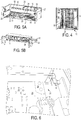
- FIG. 4 shows a top view showing internal components of the IED of FIG. 1A .
- FIG. 5A shows analog input modules (AIM) 14, 14' and a communication (COM) card 16 of the IED of FIG. 4 , now mounted in the IED housing 12 of FIG. 2 .
- FIG. 5B shows a Power Supply Module (PSM) 18 and a Binary Input/Output (BIO) module 20 of the IED of FIG. 4 , shown ready to be mounted in the IED housing 12 of FIG. 5A .
- PSM Power Supply Module
- BIO Binary Input/Output
- the AIM boards or modules 14, 14' are fixed in a horizontally adjacent manner to the bottom panel 21 inside of the housing 12 using L brackets 22 and U brackets 23.
- Manual wiring, shown for example at 27, electrically connects the modules 14, 14' to the connectors 24 in electrical communication with connections accessible at the back panel 25 of the housing 12.
- the primary current transformers (CTs) 26 are connected to one of the modules, e.g., module 14.
- the AIM modules 14, 14' can be wired with or without a Make-Before-Break (MBB) interface while maintaining full functionality and protection for the secondary CT winding. This is achieved by allowing the assembly of the boards that hold the primary CTs to be either removable in a draw-out mechanism, or be fixed within the housing 12 with constant contact with the secondary CTs and hence does not need a MBB mechanism.
- MBB Make-Before-Break
- grounding structure for electrically grounding the AIM module 14, is shown generally indicated at 28.
- the grounding structure 28 includes a metal, spring-loaded clip 30 fixed to a metal bracket 23, which is used to mount the module 14 to the metal bottom panel 21.
- a corner of the printed circuit board (PCB) 29 of the module 14 includes a grounding pad 34, defining the grounding contact area for the module 14.
- the grounding pad 34 is moved into engagement with the clip 30.
- the spring function the clip 30 keeps it engaged with the grounding pad 34 to thereby electrically ground the module 14.
- Similar grounding structure 28 can be used to ground the module 14'.
- the innovative horizontal mounting of the AIMs 14, 14' and manual wiring provides the following:
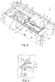
- the PSM 18 the BIO circuit board or module 20 are shown mounted in a horizontally adjacent manner to a tray 38 that is coupled to a front panel 40.
- the new front panel 40 for operator input, is coupled to an open end 42 of the housing 12 ( FIG. 8 ).
- the entire assembly of FIG. 7 is removable or can be drawn-out from the housing 12 for maintenance and/or for accessing the AIM modules 14, 14' that are spaced below the tray 38 in the IED 10' of FIG. 8 .
- a protective cover 44 is provided over the module 18 and a second protective cover 46 is provided over the module 20.
- the covers 44, 46 provide EMC immunity to the PSM and BIO module.
- the covers 44, 46 also allow the use of guide rails 45 inside the covers, which help in the alignment of the modules 18, 20 with respect to the connectors on the backplane 36.
- Grounding is provided through stand-offs connecting the metal tray 38 to plated ground holes on the PSM and BIO circuit boards.
- the covers are secured to the tray 38 by metal screws.
- the tray 38 is engaged with electrically conductive guide rails 47 that are connected to the housing 12.
- the modules 18 and 20 are of the type configured for vertical mounting in housing 11 ( FIG. 1A ) and include current or updated technology.
- first adaptor structure generally indicated at 48 ( FIG. 7 )
- the first adaptor structure 48 is preferably a rigid printed circuit board 50 having connectors 52 thereon that receive mating connectors 54 of the modules 18 and 20, which would otherwise been connect directly to connectors 13 associated with the back panel 56 of the IED 10 of FIG. 1B .
- the circuit board 50 is also connected to associated connectors 58 that are in electrical communication with certain of the connections on the back panel 25 of the housing 12.
- circuit board 50 bridges the physical gap between the modules 18 and 20 and the back panel 25. Connection between PSM and BIO module to the external Input/outputs is achieved through the circuit board 50. It is noted that the covers 44 and 46 are not shown in FIG. 8 for clarity of illustration.
- a second adaptor structure 48' is employed to connect the communication (COM) circuit board or card 16 to the backplane 36 rather than connecting the COM card 16 directly to the backplane as in the IED 10 of FIG. 1A .
- the second adaptor structure 48' is preferably a rigid printed circuit board 60 having a connector 62 that receives a mating portion of the COM card 16.
- a portion 64 of the circuit board 60 is electrically received by an associated connector 66 of the backplane 36, which is adjacent to the front panel 40 of the housing 12.
- the circuit board 60 bridges the physical gap between the COM card 16 and the backplane 36.
- This arrangement facilitates the access of the COM ports 68 ( FIG. 3 ) from the back panel 25 by providing the ports 68 in the same plane like other rear terminals.
- the COM card 16 is fixed to the housing 12 by using a mounting holder 51 hanging from the top panel (not shown) of the housing 12.
- the utilization of the adapter structures 48, 48' to electrically connect the hardware modules 18, 20 (configured for a first form factor) within the housing 12 (configured for a second form fact that is different from the first form factor), allows power utilities to adopt state of the art technology for their IEDs, without the need to change the physical wiring locations and input/output interface associated with the housing 12.
- FIG. 9 shows grounding structure including a metal spring 68 fixed to a metal bracket 70 that is fixed to a metal side 72 of the housing 12.
- a corner of the printed circuit board 50 includes a grounding pad 74, defining the grounding contact area for the module 14.
- the grounding pad 74 is moved into engagement with the spring 68.
- the spring force of the spring 68 keeps it engaged with the grounding pad 74 to thereby electrically ground the adaptor structure 48.
- Similar grounding structure can be used to ground the adaptor structure 48'.
- circuit boards instead of using circuit boards as the first and second adaptor structures, ribbons, flexible cables, or flexible circuit boards can be employed having the appropriate electrical connections.
Landscapes
- Engineering & Computer Science (AREA)
- Microelectronics & Electronic Packaging (AREA)
- Automation & Control Theory (AREA)
- Manufacturing & Machinery (AREA)
- Mounting Of Printed Circuit Boards And The Like (AREA)
- Structure Of Telephone Exchanges (AREA)
Claims (18)
- Verfahren zum Versehen einer intelligenten elektronischen Vorrichtung (intelligent electronic device - IED) mit neuen Hardwaremodulen, wobei das Verfahren Folgendes umfasst:Bereitstellen von Hardwaremodulen, einschließlich eines Paares von Analogeingabemodulen (analog input modules - AIMs) (14, 14'), eines Stromversorgungsmoduls (power supply module - PSM) (18) und eines binären Eingabe-/Ausgabe(binary input/output- BIO)-Moduls (20), wobei jedes Modul zum Montieren in einer vertikalen Anordnung in einem ersten IED-Gehäuse (11) konfiguriert ist, das einen ersten Formfaktor aufweist, wobei das PSM(18)- und das BIO(20)-Moduljeweils konstruiert und angeordnet sind, um sich mit elektrischen Verbindungen des ersten IED-Gehäuses (11) direkt zu verbinden,Bereitstellen eines zweiten IED-Gehäuses (12), das einen zweiten Formfaktor aufweist, der sich von dem ersten Formfaktor unterscheidet,Montieren der AIMs (14, 14') in dem zweiten IED-Gehäuse (12),Verdrahten der AIMs (14, 14') mit Verbindungen (24) an einer Rückplatte (25) des zweiten IED-Gehäuses (12),Montieren des PSM(18)- und des BIO(20)-Moduls in dem zweiten IED-Gehäuse (12) undNutzen einer Adapterstruktur (48), um das PSM(18)- und das BIO(20)-Modul mit zugehörigen Verbindungen (58) des zweiten IED-Gehäuses (12) elektrisch zu verbinden;wobei das Verfahren dadurch gekennzeichnet ist, dass der Schritt des Montierens der AIMs (14, 14') ein Befestigen der AIMs in einer horizontal angrenzenden Weise an einer Bodenplatte (21) des zweiten IED-Gehäuses (12) einschließt.
- Verfahren nach Anspruch 1, das ferner den Schritt des Montierens des zweiten IED-Gehäuses (12) in eine vorhandene Verdrahtung und eine zweite Formfaktorumgebung umfasst.
- Verfahren nach Anspruch 1, wobei der Schritt des Nutzens der Adapterstruktur (48) ein elektrisches Verbinden einer ersten Adapterstruktur (48) zwischen dem PSM(18)- und dem BIO(20)-Modul und den Verbindern (58) an einer Rückplatte (25) des zweiten IED-Gehäuses (12) einschließt.
- Verfahren nach Anspruch 3, das ferner die folgenden Schritte umfasst:Bereitstellen einer Kommunikations(communications - COM)-Karte (16), die Kommunikationsports (68) aufweist, die an einer Rückplatte (25) des zweiten IED-Gehäuses (12) zugänglich sind, undNutzen einer zweiten Adapterstruktur (48'), die zwischen der COM-Karte (16) und einem Verbinder (62) einer Rückwandplatine (36) angrenzend an eine Frontplatte (40) des zweiten IED-Gehäuses (12) elektrisch verbunden ist.
- Verfahren nach Anspruch 4, wobei die Schritte des Nutzens der ersten (48) und der zweiten (48') Adapterstruktur ein Verwenden einer Leiterplatte (50, 60) als jede Adapterstruktur einschließen.
- Verfahren nach Anspruch 1, wobei der Schritt des Montierens des PSM(18)- und des BIO(20)-Moduls das Montieren des PSM- und des BIO-Moduls in einer horizontal angrenzenden Weise an ein Fach (38) und das Montieren des Fachs (38) an das zweite IED-Gehäuse (12) in einer entfernbaren Weise umfasst, wobei das Fach (38) über den AIMs (14, 14') beabstandet ist und wobei das Fach (38) mit einer Frontplatte (40) des zweiten IED-Gehäuses (12) gekoppelt ist.
- Verfahren nach Anspruch 1, das ferner den Schritt eines elektrischen Erdens jedes der Hardwaremodule (14, 14', 18, 20) und der Adapterstruktur (48) durch das zweite IED-Gehäuse (12) umfasst.
- Verfahren nach Anspruch 7, wobei der Schritt des Erdens wenigstens eines der AIMs (14, 14') die folgenden Schritte umfasst:Koppeln eines federbelasteten Metallklipps (30) mit einer Halterung (23), die das AIM mit einer Bodenplatte (21) des zweiten IED-Gehäuses (12) koppelt,Bereitstellen eines Erdungspads (34) auf einer Oberfläche des AIM, undIneingriffnehmen des Klipps (30) mit dem Erdungspad (34).
- Verfahren nach Anspruch 1, das ferner den Schritt des Verbindens von Primärstromwandlern (26) mit einem der AIMs umfasst.
- Intelligente elektronische Vorrichtung (IED), die Folgendes umfasst:mehrere Hardwaremodule, einschließlich eines Paares von Analogeingabemodulen (AIMs) (14, 14'), eines Stromversorgungsmoduls (PSM) (18) und eines binären Eingabe-/Ausgabe(BIO)-Moduls (20), wobei jedes Modul zum Montieren in einer vertikalen Anordnung in einem ersten IED-Gehäuse (11) konfiguriert ist, das einen ersten Formfaktor aufweist, wobei das PSM(18)- und das BIO(20)-Modul konstruiert und angeordnet sind, um sich mit elektrischen Verbindungen des ersten IED-Gehäuses (11) direkt zu verbinden,ein zweites IED-Gehäuse (12), das einen zweiten Formfaktor aufweist, der sich von dem ersten Formfaktor unterscheidet, wobei die AIMs an eine Bodenplatte (21) des zweiten Gehäuses montiert sind, wobei das PSM(18)- und das BIO(20)-Modul in dem zweiten IED-Gehäuse (12) montiert sind,die Verdrahtung (27), die die AIMs (14, 14') mit Verbindungen (24) auf dem zweiten IED-Gehäuse (12) verbindet,und eine Adapterstruktur (48), die das PSM(18)- und das BIO(20)-Modul mit zugehörigen Verbindungen (58) des zweiten IED-Gehäuses (12) elektrisch verbindet;dadurch gekennzeichnet, dass die AIMs in einer horizontal angrenzenden Weise an einer Bodenplatte (21) des zweiten IED-Gehäuses (12) befestigt sind.
- Vorrichtung nach Anspruch 10, wobei die Adapterstruktur eine erste Adapterstruktur (48), die zwischen dem PSM(18)- und dem BIO(20)-Modul elektrisch verbunden ist, und die zugehörigen Verbinder (58) an einer Rückplatte (25) des zweiten IED-Gehäuses (12) einschließt.
- Vorrichtung nach Anspruch 11, die ferner Folgendes umfasst:eine Kommunikations(COM)-Karte (16), die Kommunikationsports (68) aufweist, die an einer Rückplatte (25) des zweiten IED-Gehäuses (12) zugänglich sind, undeine zweite Adapterstruktur (48'), die zwischen der COM-Karte (16) und einem Verbinder (62) einer Rückwandplatine (36) angrenzend an eine Frontplatte (40) des zweiten IED-Gehäuses (12) elektrisch verbunden ist.
- Vorrichtung nach Anspruch 12, wobei jede der ersten und der zweiten Adapterstruktur (48, 48') eine Leiterplatte (50, 60) einschließt.
- Vorrichtung nach Anspruch 10, wobei das PSM(18)- und das BIO(20)-Modul in einer horizontal angrenzenden Weise an ein Fach (38) montiert sind und das Fach (38) an das zweite IED-Gehäuse (12) in einer entfernbaren Weise montiert ist, wobei das Fach (38) über den AIMs beabstandet ist und wobei das Fach mit einer Frontplatte (40) des zweiten IED-Gehäuses (12) gekoppelt ist.
- Vorrichtung nach Anspruch 10, die ferner eine Erdungsstruktur (28) umfasst, die jedes der Hardwaremodule (14, 14', 18, 20) und die Adapterstruktur (48) durch das zweite IED-Gehäuse (12) elektrisch erdet.
- Vorrichtung nach Anspruch 17, wobei die Erdungsstruktur (28) einen federbelasteten Metallklipp (30), der mit einer Halterung (23) gekoppelt ist, die das AIM mit einer Bodenplatte (21) des zweiten IED-Gehäuses (12) koppelt, und ein Erdungspad (34) auf einer Oberfläche des AIM einschließt, wobei der Klipp (30) das Pad (34) in Eingriff nimmt.
- Vorrichtung nach Anspruch 10, die ferner Primärstromwandler (26) umfasst, die mit einem der AIMs (14, 14') verbunden sind.
- Vorrichtung nach Anspruch 10, wobei das zweite IED-Gehäuse (12) eine Höhe von 13,26 cm, eine Breite von 43,48 cm und eine Tiefe von 22,86 cm aufweist.
Applications Claiming Priority (2)
| Application Number | Priority Date | Filing Date | Title |
|---|---|---|---|
| US14/013,077 US9510475B2 (en) | 2013-08-29 | 2013-08-29 | Mechanical assembly and method to provide form-factor and wire alike adaptation of existing platform hardware modules into new products |
| PCT/US2014/052599 WO2015031294A1 (en) | 2013-08-29 | 2014-08-26 | Mechanical assembly and method to provide form-factor and wire alike adaptation of existing platform hardware modules into new products |
Publications (2)
| Publication Number | Publication Date |
|---|---|
| EP3039953A1 EP3039953A1 (de) | 2016-07-06 |
| EP3039953B1 true EP3039953B1 (de) | 2021-03-31 |
Family
ID=51519178
Family Applications (1)
| Application Number | Title | Priority Date | Filing Date |
|---|---|---|---|
| EP14761931.6A Active EP3039953B1 (de) | 2013-08-29 | 2014-08-26 | Mechanische anordnung und verfahren zur bereitstellung eines formfaktors und zur verdrahtungsanpassung vorhandener plattform-hardwaremodule zu neuen produkten |
Country Status (4)
| Country | Link |
|---|---|
| US (1) | US9510475B2 (de) |
| EP (1) | EP3039953B1 (de) |
| CN (1) | CN105612823B (de) |
| WO (1) | WO2015031294A1 (de) |
Families Citing this family (2)
| Publication number | Priority date | Publication date | Assignee | Title |
|---|---|---|---|---|
| CN106371530A (zh) * | 2016-09-07 | 2017-02-01 | 英业达科技有限公司 | 服务器 |
| USD877699S1 (en) * | 2017-04-27 | 2020-03-10 | Abb Schweiz Ag | Electric control device for power distribution |
Family Cites Families (14)
| Publication number | Priority date | Publication date | Assignee | Title |
|---|---|---|---|---|
| ATE142407T1 (de) | 1993-11-12 | 1996-09-15 | Siemens Ag | Einrichtung für eine elektronikbox zur aufnahme weiterer elektronischer baugruppen |
| US6243273B1 (en) | 1999-09-01 | 2001-06-05 | Nortel Networks Limited | Mini-backplane “T” assembly |
| DE10001815A1 (de) | 2000-01-18 | 2001-07-19 | Alcatel Sa | Vorrichtung zur Nachrüstung eines Computers |
| DE10202917A1 (de) | 2002-01-25 | 2003-08-14 | Fujitsu Siemens Computers Gmbh | Serverrack |
| FI119073B (fi) | 2003-05-06 | 2008-07-15 | Abb Oy | Pistoyksikön lukitus- ja irrotusmekanismi |
| FI119074B (fi) | 2003-05-06 | 2008-07-15 | Abb Oy | Kiinnitysmekanismi kotelon kiinnittämiseksi seinämässä olevaan aukkoon |
| FI115949B (fi) | 2003-05-09 | 2005-08-15 | Abb Oy | Järjestely komponenttien kiinnittämiseksi irrotettavasti runko-osaan |
| US20070067119A1 (en) * | 2005-09-16 | 2007-03-22 | Power Measurement Ltd. | Rack-mounted power meter having removable metering options module |
| DE102005044712B4 (de) | 2005-09-19 | 2022-02-03 | Airbus Operations Gmbh | Avionikgeräteträgersystem mit Schnelleinbaugehäuse und Schnelleinbaumodulen |
| US8769808B2 (en) * | 2005-10-17 | 2014-07-08 | Alcatel Lucent | Method for fixed and replaceable module architecture |
| EP2246954A1 (de) | 2009-04-30 | 2010-11-03 | ABB Research Ltd | Intelligente elektronische Vorrichtung mit Wechselspeichermodule zur Automatisierungssystem einer Schaltanlage |
| TWI387869B (zh) * | 2009-09-10 | 2013-03-01 | Ind Tech Res Inst | 工業模組化裝置 |
| EP2389054B1 (de) | 2010-05-19 | 2014-08-06 | ABB Technology AG | Einsteckanordnung |
| USD683706S1 (en) | 2010-09-23 | 2013-06-04 | Abb Oy | Protective relay |
-
2013
- 2013-08-29 US US14/013,077 patent/US9510475B2/en active Active
-
2014
- 2014-08-26 CN CN201480055143.0A patent/CN105612823B/zh active Active
- 2014-08-26 EP EP14761931.6A patent/EP3039953B1/de active Active
- 2014-08-26 WO PCT/US2014/052599 patent/WO2015031294A1/en active Application Filing
Non-Patent Citations (1)
| Title |
|---|
| None * |
Also Published As
| Publication number | Publication date |
|---|---|
| EP3039953A1 (de) | 2016-07-06 |
| CN105612823B (zh) | 2019-03-01 |
| WO2015031294A1 (en) | 2015-03-05 |
| CN105612823A (zh) | 2016-05-25 |
| US20150062833A1 (en) | 2015-03-05 |
| US9510475B2 (en) | 2016-11-29 |
Similar Documents
| Publication | Publication Date | Title |
|---|---|---|
| US6347963B1 (en) | Interchangeable backplane interface connection panel | |
| US11901681B2 (en) | Power distribution unit system incorporating smart cables and adapters | |
| US10980145B2 (en) | Hot-pluggable connection for data communications | |
| US6826036B2 (en) | Modular power distribution system for use in computer equipment racks | |
| US8876548B2 (en) | Rack unit outlet spacing for power outlet units | |
| CN109672049B (zh) | 柔性且可构型的机架配电单元 | |
| US20100048037A1 (en) | Telescopic power connector | |
| US11375636B2 (en) | Power distribution unit with cord storage cartridge | |
| US11039224B2 (en) | Telecommunication appliance having high density embedded pluggable optics | |
| US9451719B2 (en) | U form-factor intelligent electronic device (IED) hardware platform with matching of IED wiring, from a non U form-factor IED hardware platform using adapter structure | |
| EP3039953B1 (de) | Mechanische anordnung und verfahren zur bereitstellung eines formfaktors und zur verdrahtungsanpassung vorhandener plattform-hardwaremodule zu neuen produkten | |
| CN111244689A (zh) | 通信系统的电力连接器组件 | |
| US9723744B1 (en) | Information technology racks with integrated data signal and power distribution | |
| US9252548B1 (en) | High density networking component for 1U product form factor and associated rack system | |
| US10483664B2 (en) | Electronic terminal block for a data bus | |
| US20230109006A1 (en) | Systems, methods, and devices for replaceable elements within network switches | |
| CN117880657A (zh) | 交换网板组件、通信设备和交换网板组件的制作方法 | |
| JP4552729B2 (ja) | 通信機器 | |
| JPS61173475A (ja) | 確実なデ−タ伝送接続を形成するためのアダプタシステム | |
| EP1244313A1 (de) | Baugruppenträger für eine Telekommunikationsanlage |
Legal Events
| Date | Code | Title | Description |
|---|---|---|---|
| PUAI | Public reference made under article 153(3) epc to a published international application that has entered the european phase |
Free format text: ORIGINAL CODE: 0009012 |
|
| 17P | Request for examination filed |
Effective date: 20160225 |
|
| AK | Designated contracting states |
Kind code of ref document: A1 Designated state(s): AL AT BE BG CH CY CZ DE DK EE ES FI FR GB GR HR HU IE IS IT LI LT LU LV MC MK MT NL NO PL PT RO RS SE SI SK SM TR |
|
| AX | Request for extension of the european patent |
Extension state: BA ME |
|
| STAA | Information on the status of an ep patent application or granted ep patent |
Free format text: STATUS: REQUEST FOR EXAMINATION WAS MADE |
|
| DAX | Request for extension of the european patent (deleted) | ||
| RAP1 | Party data changed (applicant data changed or rights of an application transferred) |
Owner name: ABB SCHWEIZ AG |
|
| STAA | Information on the status of an ep patent application or granted ep patent |
Free format text: STATUS: EXAMINATION IS IN PROGRESS |
|
| 17Q | First examination report despatched |
Effective date: 20190521 |
|
| GRAP | Despatch of communication of intention to grant a patent |
Free format text: ORIGINAL CODE: EPIDOSNIGR1 |
|
| STAA | Information on the status of an ep patent application or granted ep patent |
Free format text: STATUS: GRANT OF PATENT IS INTENDED |
|
| INTG | Intention to grant announced |
Effective date: 20210112 |
|
| GRAS | Grant fee paid |
Free format text: ORIGINAL CODE: EPIDOSNIGR3 |
|
| GRAA | (expected) grant |
Free format text: ORIGINAL CODE: 0009210 |
|
| STAA | Information on the status of an ep patent application or granted ep patent |
Free format text: STATUS: THE PATENT HAS BEEN GRANTED |
|
| RAP1 | Party data changed (applicant data changed or rights of an application transferred) |
Owner name: ABB SCHWEIZ AG |
|
| AK | Designated contracting states |
Kind code of ref document: B1 Designated state(s): AL AT BE BG CH CY CZ DE DK EE ES FI FR GB GR HR HU IE IS IT LI LT LU LV MC MK MT NL NO PL PT RO RS SE SI SK SM TR |
|
| REG | Reference to a national code |
Ref country code: GB Ref legal event code: FG4D Ref country code: CH Ref legal event code: EP |
|
| REG | Reference to a national code |
Ref country code: AT Ref legal event code: REF Ref document number: 1378458 Country of ref document: AT Kind code of ref document: T Effective date: 20210415 |
|
| REG | Reference to a national code |
Ref country code: DE Ref legal event code: R096 Ref document number: 602014076165 Country of ref document: DE |
|
| REG | Reference to a national code |
Ref country code: FI Ref legal event code: FGE |
|
| REG | Reference to a national code |
Ref country code: IE Ref legal event code: FG4D |
|
| REG | Reference to a national code |
Ref country code: LT Ref legal event code: MG9D |
|
| PG25 | Lapsed in a contracting state [announced via postgrant information from national office to epo] |
Ref country code: NO Free format text: LAPSE BECAUSE OF FAILURE TO SUBMIT A TRANSLATION OF THE DESCRIPTION OR TO PAY THE FEE WITHIN THE PRESCRIBED TIME-LIMIT Effective date: 20210630 Ref country code: BG Free format text: LAPSE BECAUSE OF FAILURE TO SUBMIT A TRANSLATION OF THE DESCRIPTION OR TO PAY THE FEE WITHIN THE PRESCRIBED TIME-LIMIT Effective date: 20210630 Ref country code: HR Free format text: LAPSE BECAUSE OF FAILURE TO SUBMIT A TRANSLATION OF THE DESCRIPTION OR TO PAY THE FEE WITHIN THE PRESCRIBED TIME-LIMIT Effective date: 20210331 |
|
| PG25 | Lapsed in a contracting state [announced via postgrant information from national office to epo] |
Ref country code: SE Free format text: LAPSE BECAUSE OF FAILURE TO SUBMIT A TRANSLATION OF THE DESCRIPTION OR TO PAY THE FEE WITHIN THE PRESCRIBED TIME-LIMIT Effective date: 20210331 Ref country code: RS Free format text: LAPSE BECAUSE OF FAILURE TO SUBMIT A TRANSLATION OF THE DESCRIPTION OR TO PAY THE FEE WITHIN THE PRESCRIBED TIME-LIMIT Effective date: 20210331 Ref country code: LV Free format text: LAPSE BECAUSE OF FAILURE TO SUBMIT A TRANSLATION OF THE DESCRIPTION OR TO PAY THE FEE WITHIN THE PRESCRIBED TIME-LIMIT Effective date: 20210331 |
|
| REG | Reference to a national code |
Ref country code: NL Ref legal event code: MP Effective date: 20210331 |
|
| REG | Reference to a national code |
Ref country code: AT Ref legal event code: MK05 Ref document number: 1378458 Country of ref document: AT Kind code of ref document: T Effective date: 20210331 |
|
| PG25 | Lapsed in a contracting state [announced via postgrant information from national office to epo] |
Ref country code: SM Free format text: LAPSE BECAUSE OF FAILURE TO SUBMIT A TRANSLATION OF THE DESCRIPTION OR TO PAY THE FEE WITHIN THE PRESCRIBED TIME-LIMIT Effective date: 20210331 Ref country code: LT Free format text: LAPSE BECAUSE OF FAILURE TO SUBMIT A TRANSLATION OF THE DESCRIPTION OR TO PAY THE FEE WITHIN THE PRESCRIBED TIME-LIMIT Effective date: 20210331 Ref country code: NL Free format text: LAPSE BECAUSE OF FAILURE TO SUBMIT A TRANSLATION OF THE DESCRIPTION OR TO PAY THE FEE WITHIN THE PRESCRIBED TIME-LIMIT Effective date: 20210331 Ref country code: CZ Free format text: LAPSE BECAUSE OF FAILURE TO SUBMIT A TRANSLATION OF THE DESCRIPTION OR TO PAY THE FEE WITHIN THE PRESCRIBED TIME-LIMIT Effective date: 20210331 Ref country code: EE Free format text: LAPSE BECAUSE OF FAILURE TO SUBMIT A TRANSLATION OF THE DESCRIPTION OR TO PAY THE FEE WITHIN THE PRESCRIBED TIME-LIMIT Effective date: 20210331 Ref country code: AT Free format text: LAPSE BECAUSE OF FAILURE TO SUBMIT A TRANSLATION OF THE DESCRIPTION OR TO PAY THE FEE WITHIN THE PRESCRIBED TIME-LIMIT Effective date: 20210331 |
|
| PG25 | Lapsed in a contracting state [announced via postgrant information from national office to epo] |
Ref country code: IS Free format text: LAPSE BECAUSE OF FAILURE TO SUBMIT A TRANSLATION OF THE DESCRIPTION OR TO PAY THE FEE WITHIN THE PRESCRIBED TIME-LIMIT Effective date: 20210731 Ref country code: ES Free format text: LAPSE BECAUSE OF FAILURE TO SUBMIT A TRANSLATION OF THE DESCRIPTION OR TO PAY THE FEE WITHIN THE PRESCRIBED TIME-LIMIT Effective date: 20210331 Ref country code: PT Free format text: LAPSE BECAUSE OF FAILURE TO SUBMIT A TRANSLATION OF THE DESCRIPTION OR TO PAY THE FEE WITHIN THE PRESCRIBED TIME-LIMIT Effective date: 20210802 Ref country code: PL Free format text: LAPSE BECAUSE OF FAILURE TO SUBMIT A TRANSLATION OF THE DESCRIPTION OR TO PAY THE FEE WITHIN THE PRESCRIBED TIME-LIMIT Effective date: 20210331 Ref country code: RO Free format text: LAPSE BECAUSE OF FAILURE TO SUBMIT A TRANSLATION OF THE DESCRIPTION OR TO PAY THE FEE WITHIN THE PRESCRIBED TIME-LIMIT Effective date: 20210331 Ref country code: SK Free format text: LAPSE BECAUSE OF FAILURE TO SUBMIT A TRANSLATION OF THE DESCRIPTION OR TO PAY THE FEE WITHIN THE PRESCRIBED TIME-LIMIT Effective date: 20210331 |
|
| REG | Reference to a national code |
Ref country code: DE Ref legal event code: R097 Ref document number: 602014076165 Country of ref document: DE |
|
| PG25 | Lapsed in a contracting state [announced via postgrant information from national office to epo] |
Ref country code: DK Free format text: LAPSE BECAUSE OF FAILURE TO SUBMIT A TRANSLATION OF THE DESCRIPTION OR TO PAY THE FEE WITHIN THE PRESCRIBED TIME-LIMIT Effective date: 20210331 Ref country code: AL Free format text: LAPSE BECAUSE OF FAILURE TO SUBMIT A TRANSLATION OF THE DESCRIPTION OR TO PAY THE FEE WITHIN THE PRESCRIBED TIME-LIMIT Effective date: 20210331 |
|
| PLBE | No opposition filed within time limit |
Free format text: ORIGINAL CODE: 0009261 |
|
| STAA | Information on the status of an ep patent application or granted ep patent |
Free format text: STATUS: NO OPPOSITION FILED WITHIN TIME LIMIT |
|
| 26N | No opposition filed |
Effective date: 20220104 |
|
| REG | Reference to a national code |
Ref country code: CH Ref legal event code: PL |
|
| PG25 | Lapsed in a contracting state [announced via postgrant information from national office to epo] |
Ref country code: MC Free format text: LAPSE BECAUSE OF FAILURE TO SUBMIT A TRANSLATION OF THE DESCRIPTION OR TO PAY THE FEE WITHIN THE PRESCRIBED TIME-LIMIT Effective date: 20210331 |
|
| REG | Reference to a national code |
Ref country code: BE Ref legal event code: MM Effective date: 20210831 |
|
| GBPC | Gb: european patent ceased through non-payment of renewal fee |
Effective date: 20210826 |
|
| PG25 | Lapsed in a contracting state [announced via postgrant information from national office to epo] |
Ref country code: LI Free format text: LAPSE BECAUSE OF NON-PAYMENT OF DUE FEES Effective date: 20210831 Ref country code: CH Free format text: LAPSE BECAUSE OF NON-PAYMENT OF DUE FEES Effective date: 20210831 |
|
| PG25 | Lapsed in a contracting state [announced via postgrant information from national office to epo] |
Ref country code: IS Free format text: LAPSE BECAUSE OF FAILURE TO SUBMIT A TRANSLATION OF THE DESCRIPTION OR TO PAY THE FEE WITHIN THE PRESCRIBED TIME-LIMIT Effective date: 20210731 Ref country code: LU Free format text: LAPSE BECAUSE OF NON-PAYMENT OF DUE FEES Effective date: 20210826 |
|
| PG25 | Lapsed in a contracting state [announced via postgrant information from national office to epo] |
Ref country code: IE Free format text: LAPSE BECAUSE OF NON-PAYMENT OF DUE FEES Effective date: 20210826 Ref country code: GB Free format text: LAPSE BECAUSE OF NON-PAYMENT OF DUE FEES Effective date: 20210826 Ref country code: BE Free format text: LAPSE BECAUSE OF NON-PAYMENT OF DUE FEES Effective date: 20210831 |
|
| PG25 | Lapsed in a contracting state [announced via postgrant information from national office to epo] |
Ref country code: HU Free format text: LAPSE BECAUSE OF FAILURE TO SUBMIT A TRANSLATION OF THE DESCRIPTION OR TO PAY THE FEE WITHIN THE PRESCRIBED TIME-LIMIT; INVALID AB INITIO Effective date: 20140826 |
|
| PG25 | Lapsed in a contracting state [announced via postgrant information from national office to epo] |
Ref country code: CY Free format text: LAPSE BECAUSE OF FAILURE TO SUBMIT A TRANSLATION OF THE DESCRIPTION OR TO PAY THE FEE WITHIN THE PRESCRIBED TIME-LIMIT Effective date: 20210331 |
|
| PG25 | Lapsed in a contracting state [announced via postgrant information from national office to epo] |
Ref country code: GR Free format text: LAPSE BECAUSE OF FAILURE TO SUBMIT A TRANSLATION OF THE DESCRIPTION OR TO PAY THE FEE WITHIN THE PRESCRIBED TIME-LIMIT Effective date: 20210331 |
|
| PGFP | Annual fee paid to national office [announced via postgrant information from national office to epo] |
Ref country code: IT Payment date: 20230825 Year of fee payment: 10 Ref country code: FI Payment date: 20230821 Year of fee payment: 10 |
|
| PGFP | Annual fee paid to national office [announced via postgrant information from national office to epo] |
Ref country code: FR Payment date: 20230825 Year of fee payment: 10 Ref country code: DE Payment date: 20230821 Year of fee payment: 10 |
|
| PG25 | Lapsed in a contracting state [announced via postgrant information from national office to epo] |
Ref country code: MK Free format text: LAPSE BECAUSE OF FAILURE TO SUBMIT A TRANSLATION OF THE DESCRIPTION OR TO PAY THE FEE WITHIN THE PRESCRIBED TIME-LIMIT Effective date: 20210331 |