EP3038438B1 - Leiterplatte und motorantriebsvorrichtung mit der leiterplatte - Google Patents
Leiterplatte und motorantriebsvorrichtung mit der leiterplatte Download PDFInfo
- Publication number
- EP3038438B1 EP3038438B1 EP15201535.0A EP15201535A EP3038438B1 EP 3038438 B1 EP3038438 B1 EP 3038438B1 EP 15201535 A EP15201535 A EP 15201535A EP 3038438 B1 EP3038438 B1 EP 3038438B1
- Authority
- EP
- European Patent Office
- Prior art keywords
- heat
- pattern
- phase switch
- thermistor element
- circuit board
- Prior art date
- Legal status (The legal status is an assumption and is not a legal conclusion. Google has not performed a legal analysis and makes no representation as to the accuracy of the status listed.)
- Active
Links
Images



Classifications
-
- H—ELECTRICITY
- H05—ELECTRIC TECHNIQUES NOT OTHERWISE PROVIDED FOR
- H05K—PRINTED CIRCUITS; CASINGS OR CONSTRUCTIONAL DETAILS OF ELECTRIC APPARATUS; MANUFACTURE OF ASSEMBLAGES OF ELECTRICAL COMPONENTS
- H05K1/00—Printed circuits
- H05K1/02—Details
- H05K1/0201—Thermal arrangements, e.g. for cooling, heating or preventing overheating
- H05K1/0203—Cooling of mounted components
- H05K1/0209—External configuration of printed circuit board adapted for heat dissipation, e.g. lay-out of conductors, coatings
-
- H—ELECTRICITY
- H02—GENERATION; CONVERSION OR DISTRIBUTION OF ELECTRIC POWER
- H02K—DYNAMO-ELECTRIC MACHINES
- H02K11/00—Structural association of dynamo-electric machines with electric components or with devices for shielding, monitoring or protection
- H02K11/30—Structural association with control circuits or drive circuits
- H02K11/33—Drive circuits, e.g. power electronics
-
- H—ELECTRICITY
- H05—ELECTRIC TECHNIQUES NOT OTHERWISE PROVIDED FOR
- H05K—PRINTED CIRCUITS; CASINGS OR CONSTRUCTIONAL DETAILS OF ELECTRIC APPARATUS; MANUFACTURE OF ASSEMBLAGES OF ELECTRICAL COMPONENTS
- H05K1/00—Printed circuits
- H05K1/02—Details
- H05K1/0201—Thermal arrangements, e.g. for cooling, heating or preventing overheating
-
- H—ELECTRICITY
- H05—ELECTRIC TECHNIQUES NOT OTHERWISE PROVIDED FOR
- H05K—PRINTED CIRCUITS; CASINGS OR CONSTRUCTIONAL DETAILS OF ELECTRIC APPARATUS; MANUFACTURE OF ASSEMBLAGES OF ELECTRICAL COMPONENTS
- H05K1/00—Printed circuits
- H05K1/02—Details
-
- H—ELECTRICITY
- H02—GENERATION; CONVERSION OR DISTRIBUTION OF ELECTRIC POWER
- H02K—DYNAMO-ELECTRIC MACHINES
- H02K11/00—Structural association of dynamo-electric machines with electric components or with devices for shielding, monitoring or protection
- H02K11/02—Structural association of dynamo-electric machines with electric components or with devices for shielding, monitoring or protection for suppression of electromagnetic interference
-
- H—ELECTRICITY
- H02—GENERATION; CONVERSION OR DISTRIBUTION OF ELECTRIC POWER
- H02K—DYNAMO-ELECTRIC MACHINES
- H02K11/00—Structural association of dynamo-electric machines with electric components or with devices for shielding, monitoring or protection
- H02K11/20—Structural association of dynamo-electric machines with electric components or with devices for shielding, monitoring or protection for measuring, monitoring, testing, protecting or switching
- H02K11/25—Devices for sensing temperature, or actuated thereby
-
- H—ELECTRICITY
- H02—GENERATION; CONVERSION OR DISTRIBUTION OF ELECTRIC POWER
- H02P—CONTROL OR REGULATION OF ELECTRIC MOTORS, ELECTRIC GENERATORS OR DYNAMO-ELECTRIC CONVERTERS; CONTROLLING TRANSFORMERS, REACTORS OR CHOKE COILS
- H02P27/00—Arrangements or methods for the control of AC motors characterised by the kind of supply voltage
- H02P27/04—Arrangements or methods for the control of AC motors characterised by the kind of supply voltage using variable-frequency supply voltage, e.g. inverter or converter supply voltage
-
- H—ELECTRICITY
- H02—GENERATION; CONVERSION OR DISTRIBUTION OF ELECTRIC POWER
- H02P—CONTROL OR REGULATION OF ELECTRIC MOTORS, ELECTRIC GENERATORS OR DYNAMO-ELECTRIC CONVERTERS; CONTROLLING TRANSFORMERS, REACTORS OR CHOKE COILS
- H02P27/00—Arrangements or methods for the control of AC motors characterised by the kind of supply voltage
- H02P27/04—Arrangements or methods for the control of AC motors characterised by the kind of supply voltage using variable-frequency supply voltage, e.g. inverter or converter supply voltage
- H02P27/06—Arrangements or methods for the control of AC motors characterised by the kind of supply voltage using variable-frequency supply voltage, e.g. inverter or converter supply voltage using DC to AC converters or inverters
-
- H—ELECTRICITY
- H05—ELECTRIC TECHNIQUES NOT OTHERWISE PROVIDED FOR
- H05K—PRINTED CIRCUITS; CASINGS OR CONSTRUCTIONAL DETAILS OF ELECTRIC APPARATUS; MANUFACTURE OF ASSEMBLAGES OF ELECTRICAL COMPONENTS
- H05K1/00—Printed circuits
- H05K1/02—Details
- H05K1/0201—Thermal arrangements, e.g. for cooling, heating or preventing overheating
- H05K1/0203—Cooling of mounted components
- H05K1/0207—Cooling of mounted components using internal conductor planes parallel to the surface for thermal conduction, e.g. power planes
-
- H—ELECTRICITY
- H05—ELECTRIC TECHNIQUES NOT OTHERWISE PROVIDED FOR
- H05K—PRINTED CIRCUITS; CASINGS OR CONSTRUCTIONAL DETAILS OF ELECTRIC APPARATUS; MANUFACTURE OF ASSEMBLAGES OF ELECTRICAL COMPONENTS
- H05K7/00—Constructional details common to different types of electric apparatus
- H05K7/14—Mounting supporting structure in casing or on frame or rack
- H05K7/1422—Printed circuit boards receptacles, e.g. stacked structures, electronic circuit modules or box like frames
- H05K7/1427—Housings
- H05K7/1432—Housings specially adapted for power drive units or power converters
-
- H—ELECTRICITY
- H05—ELECTRIC TECHNIQUES NOT OTHERWISE PROVIDED FOR
- H05K—PRINTED CIRCUITS; CASINGS OR CONSTRUCTIONAL DETAILS OF ELECTRIC APPARATUS; MANUFACTURE OF ASSEMBLAGES OF ELECTRICAL COMPONENTS
- H05K7/00—Constructional details common to different types of electric apparatus
- H05K7/14—Mounting supporting structure in casing or on frame or rack
- H05K7/1422—Printed circuit boards receptacles, e.g. stacked structures, electronic circuit modules or box like frames
- H05K7/1427—Housings
- H05K7/1432—Housings specially adapted for power drive units or power converters
- H05K7/14329—Housings specially adapted for power drive units or power converters specially adapted for the configuration of power bus bars
-
- H—ELECTRICITY
- H05—ELECTRIC TECHNIQUES NOT OTHERWISE PROVIDED FOR
- H05K—PRINTED CIRCUITS; CASINGS OR CONSTRUCTIONAL DETAILS OF ELECTRIC APPARATUS; MANUFACTURE OF ASSEMBLAGES OF ELECTRICAL COMPONENTS
- H05K1/00—Printed circuits
- H05K1/02—Details
- H05K1/0201—Thermal arrangements, e.g. for cooling, heating or preventing overheating
- H05K1/0203—Cooling of mounted components
-
- H—ELECTRICITY
- H05—ELECTRIC TECHNIQUES NOT OTHERWISE PROVIDED FOR
- H05K—PRINTED CIRCUITS; CASINGS OR CONSTRUCTIONAL DETAILS OF ELECTRIC APPARATUS; MANUFACTURE OF ASSEMBLAGES OF ELECTRICAL COMPONENTS
- H05K2201/00—Indexing scheme relating to printed circuits covered by H05K1/00
- H05K2201/10—Details of components or other objects attached to or integrated in a printed circuit board
- H05K2201/10007—Types of components
- H05K2201/10022—Non-printed resistor
-
- H—ELECTRICITY
- H05—ELECTRIC TECHNIQUES NOT OTHERWISE PROVIDED FOR
- H05K—PRINTED CIRCUITS; CASINGS OR CONSTRUCTIONAL DETAILS OF ELECTRIC APPARATUS; MANUFACTURE OF ASSEMBLAGES OF ELECTRICAL COMPONENTS
- H05K2201/00—Indexing scheme relating to printed circuits covered by H05K1/00
- H05K2201/10—Details of components or other objects attached to or integrated in a printed circuit board
- H05K2201/10007—Types of components
- H05K2201/10053—Switch
-
- H—ELECTRICITY
- H05—ELECTRIC TECHNIQUES NOT OTHERWISE PROVIDED FOR
- H05K—PRINTED CIRCUITS; CASINGS OR CONSTRUCTIONAL DETAILS OF ELECTRIC APPARATUS; MANUFACTURE OF ASSEMBLAGES OF ELECTRICAL COMPONENTS
- H05K2201/00—Indexing scheme relating to printed circuits covered by H05K1/00
- H05K2201/10—Details of components or other objects attached to or integrated in a printed circuit board
- H05K2201/10007—Types of components
- H05K2201/10151—Sensor
-
- H—ELECTRICITY
- H05—ELECTRIC TECHNIQUES NOT OTHERWISE PROVIDED FOR
- H05K—PRINTED CIRCUITS; CASINGS OR CONSTRUCTIONAL DETAILS OF ELECTRIC APPARATUS; MANUFACTURE OF ASSEMBLAGES OF ELECTRICAL COMPONENTS
- H05K2201/00—Indexing scheme relating to printed circuits covered by H05K1/00
- H05K2201/10—Details of components or other objects attached to or integrated in a printed circuit board
- H05K2201/10007—Types of components
- H05K2201/10166—Transistor
-
- H—ELECTRICITY
- H05—ELECTRIC TECHNIQUES NOT OTHERWISE PROVIDED FOR
- H05K—PRINTED CIRCUITS; CASINGS OR CONSTRUCTIONAL DETAILS OF ELECTRIC APPARATUS; MANUFACTURE OF ASSEMBLAGES OF ELECTRICAL COMPONENTS
- H05K2201/00—Indexing scheme relating to printed circuits covered by H05K1/00
- H05K2201/10—Details of components or other objects attached to or integrated in a printed circuit board
- H05K2201/10007—Types of components
- H05K2201/10219—Thermoelectric component
Definitions
- Embodiments relate to a printed circuit board and a motor drive apparatus including the printed circuit board.
- a vacuum cleaner creates a suction state in the interior of a main body by driving a motor, thus causing, for example, dust to be suctioned to the interior of the main body by suction force.
- the motor used in the vacuum cleaner may be driven by drive power supplied from an inverter which includes three-phase switch elements.
- EP 2651015 A1 , WO 2012/137597 A1 and JP 2011 033479 A are related technology to the present invention.
- the three-phase switch elements show an increase in the number of switching times according to the drive time and the drive speed of the motor, and heat may be generated inside the elements.
- a copper foil layer may be formed on the printed circuit board so as to absorb and radiate the heat in the three-phase switch elements.
- the three-phase switch elements show an increase in the number of switching times according to the drive time
- Embodiments provide a printed circuit board according to independent claim 1, and a motor drive apparatus including the printed circuit board according to claim 7.
- FIG. 1 is a perspective view illustrating a portion of a printed circuit board according to an exemplary embodiment
- FIG. 2 is an exploded perspective view illustrating the printed circuit board of FIG. 1 .
- the printed circuit board 100 illustrated in FIGS. 1 and 2 indicates an inverter unit (not illustrated), which supplies drive power to a motor (not illustrated).
- the printed circuit board 100 is provided with three-phase switch elements s1, s2, s3, s4, s5 and s6 for an inverter, and a thermistor element NTC 1.
- the printed circuit board 100 includes a base layer (not illustrated), a copper foil layer 110 on the base layer, the copper foil layer 110 being formed with a circuit pattern, and an insulation layer 120 on the copper foil layer 110.
- the base layer may be formed of an FR4 material or a metal material.
- the base layer will be described as being formed of the FR4 material.
- the copper foil layer 110 includes solder patterns sp1, sp2, sp3, sp4, sp5 and sp6, to which the three-phase inverter switch elements s1, s2, s3, s4, s5 and s6 for the supply of drive power to the motor (not illustrated) are soldered, heat radiation patterns hp1 and hp2 which are spaced apart from the solder patterns sp1, sp2, sp3, sp4, sp5 and sp6 and come into contact with one surface of the respective three-phase switch elements s1, s2, s3, s4, s5 and s6 so as to absorb and radiate heat in the three-phase switch elements s1, s2, s3, s4, s5 and s6, a heat circulation pattern hs1, through which the heat absorbed by the heat radiation patterns hp1 is circulated, and element patterns (not illustrated) formed on both sides of the heat circulation pattern hs1, to which the thermistor element NTC
- solder patterns sp1, sp2, sp3, sp4, sp5 and sp6 are soldered to three terminals of the three-phase switch elements s1, s2, s3, s4, s5 and s6.
- the three-phase switch elements s1, s2, s3, s4, s5 and s6 will be described as FETs.
- the FET may include a drain, a gate and a source, and may connect the drain and the source to each other in response to a gate signal input to the gate, thereby generating a PWM signal and supplying the same to the motor.
- each of the solder patterns sp1, sp2, sp3, sp4, sp5 and sp6 is connected to three terminals of a corresponding one of the three-phase switch elements s1, s2, s3, s4, s5 and s6, and may include a signal line (not illustrated) through which a gate signal is applied to the gate of each of the three-phase switch elements s1, s2, s3, s4, s5 and s6 as described above, a power line (not illustrated) connected to the drain, and a power line (not illustrated) connected to the source, without being limited thereto.
- the heat radiation pattern hp1 comes into contact with a single surface that is common to all of the three-phase switch elements s1, s2 and s3, thereby absorbing and radiating heat in the three-phase switch elements s1, s2 and s3.
- the heat radiation pattern hp2 comes into contact with a single surface that is common to all of the three-phase switch elements s4, s5 and s6, thereby absorbing and radiating heat in the three-phase switch elements s4, s5 and s6.
- the heat circulation pattern hs1 is connected to the heat radiation pattern hp1, and circulates the heat absorbed from the heat radiation pattern hp1.
- the heat circulation pattern hs1 has been illustrated and described as being connected to any one heat radiation pattern hp1 among the heat radiation patterns hp1 and hp2, the heat circulation pattern hs1 may be connected to the heat radiation pattern hp2, without being limited thereto.
- heat radiation patterns hp1 and hp2 are illustrated as being separated from each other, the heat radiation patterns hp1 and hp2 may be formed as a single pattern, without being limited thereto.
- the heat circulation pattern hs1 may have a "U"-shaped form to enable the circulation of heat absorbed by the heat radiation pattern hp1.
- the element patterns is located close to both sides of the heat circulation pattern hs1, and the thermistor element NTC1 is soldered to the element patterns.
- the element patterns may be configured as via-hole patterns, without being limited thereto.
- the insulation layer 120 may be disposed on the copper foil layer 110, and may form open regions so1, so2, so3, so4, so5 and so6 to allow the respective three-phase switch elements s1, s2, s3, s4, s5 and s6 to be soldered to the respective solder patterns sp1, sp2, sp3, sp4, sp5 and sp6, and may also form an open region no1 to allow each thermistor element NTC1 to be soldered to the respective element patterns.
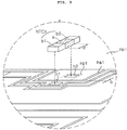
- FIG. 3 is an enlarged view of the portion "A" illustrated in FIG. 2 .
- FIG. 3 illustrates the heat radiation pattern hp1, the heat circulation pattern hs1, and the element pattern np1.
- the thermistor element NTC1 includes first and second electrode portions b1 and b2, and an insulator portion a between the first and second electrode portions b1 and b2.
- the thermistor element NTC1 will be described as being located between the second-phase and third-phase switch elements s2 and s3 among the three-phase switch elements s1, s2 and s3 so as to be close to the second-phase switch element s2.
- the thermistor element NTC1 is located close to the second-phase switch element s2, and thus may achieve the advantage of simultaneously measuring heat in the second-phase switch element s2 and heat which is absorbed and circulated through the heat circulation pattern hs1.
- first and second electrode portions b1 and b2 may be soldered to the element pattern np1.
- the insulator portion a vertically overlaps the heat circulation pattern hs1 from the upper side thereof, and indirectly reacts to the heat circulated through the heat circulation pattern hs1 such that the resistance value thereof may be varied.
- the heat radiation pattern hp1 absorbs and radiates heat in the three-phase switch elements s1, s2 and s3 as described above with reference to FIGS. 1 and 2 .
- the heat absorbed by the heat radiation pattern hp1 is conducted to the heat circulation pattern hs1, so as to be circulated through the heat circulation pattern hs1.
- the element pattern np1 may include first and second via-hole patterns h1 and h2, to which the first and second electrode portions b1 and b2 are soldered, the first and second via-hole patterns h1 and h2 being formed through the base layer (not illustrated).
- the first and second via-hole patterns h1 and h2 may be formed through a first surface of the base layer and a second surface thereof, which is opposite to the first surface.
- the second surface of the base layer may be provided with a heat measurement pattern (not illustrated), which is connected to at least one of the first and second via-hole patterns h1 and h2 such that other elements are disposed on the heat measurement pattern to measure heat based on the variable resistance value of the thermistor element NTC1, without being limited thereto.
- the width d of the insulator portion a or the distance (not illustrated) between the first and second electrode portions b1 and b2 may be greater than the width b of the heat circulation pattern hs1.
- the width d or the distance is less than the width b of the heat circulation pattern hs1, the first and second electrode portions b1 and b2 are at risk of forming a short-circuit due to the heat circulation pattern hs1.
- the abnormal operation of at least one of the three-phase switch elements s1, s2, s3, s4, s5 and s6 may be advantageously checked based on the thermal voltage measured by the NTC1 when the printed circuit board 100 is applied to a motor drive apparatus 200.
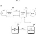
- FIG. 4 is a control block diagram illustrating the control configuration of the motor drive apparatus according to an exemplary embodiment
- FIG. 5 is a circuit diagram illustrating a first embodiment of a heat measurement unit of FIG. 4 .
- the motor drive apparatus 200 may include a converter unit 210, an inverter unit 220, a heat measurement unit 230, and a motor controller 240.
- the converter unit 210 may include a rectifier circuit which rectifies commercial power, i.e. converts AC power into DC power.
- the inverter unit 220 includes the three-phase switch elements s1, s2, s3, s4, s5 and s6, which are soldered to the solder patterns sp1, sp2, sp3, sp4, sp5 and sp6 formed on the printed circuit board 100 as described above with reference to FIGS. 1 to 3 , and come into contact, on at least one surface thereof, with the heat radiation patterns hp1 and hp2 which absorb and radiate heat, and supply drive power to a motor M.
- the three-phase switch elements s1, s2, s3, s4, s5 and s6 perform switching in response to gate signals applied from the motor controller 240, so as to output the drive power to the motor M.
- the heat measurement unit 230 is disposed on the heat circulation pattern hs1 connected to the heat radiation pattern hp1, and outputs the thermal voltage Vntc, which corresponds to the heat circulated from the heat radiation pattern hp1 to the heat circulation pattern hs1.
- the heat measurement unit 230 may include a thermistor element NTC, a reference resistor R1, and an RC resonance filter composed of a resistor R2 and a capacitor C.
- the heat measurement unit 230 will be described as measuring the thermal voltage Vntc with the thermistor element NTC1 illustrated in FIGS. 1 to 3 , and the thermistor element NTC will be described as being the thermistor element NTC1 illustrated in FIGS. 1 to 3 .
- the thermistor element NTC is soldered to the element pattern npl formed on both sides of the heat circulation pattern hs1 on the printed circuit board 100, and vertically overlaps the heat circulation pattern hs1 from the upper side thereof.
- the resistance value of the thermistor element NTC decreases in proportion to the heat.
- the reference resistor R1 may be connected to the thermistor element NTC in parallel with a distribution contact p interposed therebetween.
- the RC filter may be connected to the distribution contact p, and may remove noise from the thermal voltage Vntc applied to the distribution contact p so as to output the thermal voltage Vntc to the motor controller 240.
- the thermal voltage Vntc is a distribution voltage that is applied to the distribution contact p as a reference voltage Vcc is supplied to one side of the thermistor element NTC.
- the thermal voltage Vntc may be variable as the resistance value of the thermistor element NTC is varied by heat, and may be calculated using the following Equation 1.
- Vntc R 1 Rntc + r 1 Vcc
- Vntc indicates the thermal voltage of the thermistor element NTC
- Rntc indicates the resistance value of the thermistor element NTC
- R1 indicates the resistance value of the reference resistor
- Vcc indicates a reference voltage
- the resistance value Rntc of the thermistor element NTC is a resistance value that is varied by heat.
- the thermal voltage Vntc is 0,833 V.
- the thermal voltage Vntc may increase to 2.5 V.
- the motor controller 240 may control the inverter unit 220, and may control the driving of the motor M by comparing the thermal voltage Vntc output from the heat measurement unit 230 with a reference thermal voltage which is set to control the driving of the motor M.
- the motor controller 240 may judge that at least one of the three-phase switch elements s1, s2, s3, s4, s5 and s6 included in the inverter unit 220 is operating abnormally, and may control the three-phase switch elements s1, s2, s3, s4, s5 and s6 so as to stop the operation of the motor M.
- the motor drive device 200 may monitor the state of the three-phase switch elements s1, s2, s3, s4, s5 and s6 based on the thermal voltage Vntc corresponding to the heat in the three-phase switch elements s1, s2, s3, s4, s5 and s6, and may control the motor M so as to stop the operation of the motor M upon the abnormal operation of the switch element(s).
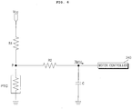
- FIG. 6 is a circuit diagram illustrating a second embodiment of the heat measurement unit of FIG. 4 .
- FIG. 6 in which configurations that are the same as those of FIGs. 4 and 5 are not illustrated and described, is a diagram of a circuit that uses a PCT thermistor, which is different from the thermistor element of FIG. 5 .
- the heat measurement unit 230 may include the thermistor element PTC, the reference resistor R1, and the RC resonance filter composed of the resistor R2 and the capacitor C.
- FIG. 6 will be described with the same reference numerals as those in FIG. 5 .
- the thermistor element PTC is soldered to the element pattern np1 formed on both sides of the heat circulation pattern hs1 on the printed circuit board 100, and vertically overlaps the heat circulation pattern hs1 from the upper side thereof.
- the thermistor element PCT may be a PCT thermistor element, the resistance value of which increases in proportion to the heat.
- the reference resistor R1 may be connected to the thermistor element PTC in parallel with the distribution contact p interposed therebetween.
- the RC filter may be connected to the distribution contact p, and may remove noise from the thermal voltage Vptc applied to the distribution contact p so as to output the thermal voltage Vptc to the motor controller 240.
- the thermal voltage Vptc is a distribution voltage that is applied to the distribution contact p by the resistance value of the thermistor element PCT as a reference voltage Vcc is supplied to one side of the reference resistor R1.
- Vptc Rptc Rptc + R 1 Vcc
- Vptc indicates the thermal voltage of the thermistor element PTC
- Rptc indicates the resistance value of the thermistor element PTC
- R1 indicates the resistance value of the reference resistor
- Vcc indicates a reference voltage
- the resistance value Rptc of the thermistor element PTC is a resistance value that is varied by heat.
- the thermal voltage Vptc is 2.5 V.
- the thermal voltage Vptc may increase to 4.167 V.
- the motor controller 240 may control the inverter unit 220, and may control the driving of the motor M by comparing the thermal voltage Vptc output from the heat measurement unit 230 with a reference thermal voltage which is set to control the driving of the motor M.
- the motor controller 240 may judge that at least one of the three-phase switch elements s1, s2, s3, s4, s5 and s6 included in the inverter unit 220 is operating abnormally, and may control the three-phase switch elements s1, s2, s3, s4, s5 and s6 so as to stop the operation of the motor M.
- the motor drive device 200 may monitor the state of the three-phase switch elements s1, s2, s3, s4, s5 and s6 based on the thermal voltage Vptc corresponding to the heat in the three-phase switch elements s1, s2, s3, s4, s5 and s6, and may control the motor M so as to stop the operation of the motor M upon the abnormal operation of the switch element(s).
- a heat radiation pattern which comes into contact with a single surface that is common to all of inverter switch elements so as to absorb and radiate heat in the inverter switch elements
- a heat circulation pattern connected to the heat radiation pattern such that the heat absorbed by the heat radiation pattern is circulated through the heat circulation pattern, and an element pattern formed on the heat circulation pattern so as to allow a thermistor element to indirectly measure the heat
- the heat in the switch elements may be advantageously measured in an indirect manner.
Landscapes
- Engineering & Computer Science (AREA)
- Microelectronics & Electronic Packaging (AREA)
- Power Engineering (AREA)
- Physics & Mathematics (AREA)
- Electromagnetism (AREA)
- Inverter Devices (AREA)
- Control Of Ac Motors In General (AREA)
- Thermal Sciences (AREA)
Claims (13)
- Leiterplatte (100) mit dreiphasigen Schaltelementen und einem Thermistorelement, wobei die Leiterplatte ferner aufweist:eine Kupferfolienschicht (100), die ein Schaltungsmuster auf einer Basisschicht bildet; undeine Isolierschicht (120), die auf die Kupferfolienschicht laminiert ist,wobei das Schaltungsmuster aufweist:eine Wechselrichtereinheit (220), die dreiphasige Schaltelemente (s1, s2, s3, s4, s5, s6) aufweist, die jeweils auf ein Lötmuster (sp1, sp2, sp3, sp4, sp5, sp6) gelötet sind;wobei das Lötmuster (sp1, sp2, sp3, sp4, sp5, sp6), an das ein Wechselrichter-Schaltelement (s1, s2, s3, s4, s5, s6) gelötet ist, Antriebsstrom an einen Motor liefern soll;ein Wärmeabstrahlungsmuster (hp1, hp2), das vom Lötmuster (sp1, sp2, sp3, sp4, sp5, sp6) beabstandet ist und eine Oberfläche des Wechselrichter-Schaltelements berühren soll, um Wärme im Wechselrichter-Schaltelement aufzunehmen und abzustrahlen;ein Wärmeumwälzungsmuster (hs1), durch das die vom Wärmeabstrahlungsmuster aufgenommene Wärme umgewälzt wird; undeine Elementmuster (np1), das auf beiden Seiten des Wärmeumwälzungsmusters ausgebildet ist, wo das Thermistorelement (NTC1 oder PTC), dessen Widerstandswert entsprechend der Wärme variiert, auf das Elementmuster gelötet ist;gekennzeichnet durchein Wärmemessmuster, um die Wärme beruhend auf dem variablen Widerstandswert des Thermistorelements (NTC1 oder PTC) zu messen,wobei das Thermistorelement (NTC oder PTC) auf dem Wärmeumwälzungsmuster so angeordnet ist, dass es sich vertikal mit dem Wärmeumwälzungsmuster überlappt, wobei das Thermistorelement in der Nähe zu einem beliebigen Schaltelement unter den dreiphasigen Schaltelementen angeordnet ist;wobei das Thermistorelement (NTC oder PTC) aufweist:einen ersten und zweiten Leiterabschnitt, die an das Elementmuster gelötet sind; undeinen Isolatorabschnitt (a), der auf dem Wärmeumwälzungsmuster so angeordnet ist, dass dessen Widerstandswert durch die Wärme variiert wird, undwobei ein Abstand zwischen dem ersten und zweiten Leiterabschnitt oder eine Breite (d) des Isolatorabschnitts größer als eine Breite (b) des Wärmeumwälzungsmusters ist.
- Leiterplatte nach Anspruch 1, wobei das Wärmeumwälzungsmuster auf mindestens einer Seite des Wärmeabstrahlungsmusters ausgebildet ist und eine U-förmige Form aufweist.
- Leiterplatte nach Anspruch 1 oder 2, wobei das Thermistorelement ein NTC-Thermistor, dessen Widerstandswert proportional zur Wärme abnimmt, oder ein PCT-Thermistor ist, dessen Widerstandswert proportional zur Wärme zunimmt.
- Leiterplatte nach Anspruch 1, wobei das Elementmuster ein erstes und zweites Durchgangslochmuster aufweist, die an den ersten und zweiten Leiterabschnitt gelötet sind.
- Leiterplatte nach Anspruch 4, wobei das erste und zweite Durchgangslochmuster durch eine erste Oberfläche der Basisschicht und eine zweite Oberfläche ausgebildet sind, die der ersten Oberfläche gegenüberliegt.
- Leiterplatte nach Anspruch 5, wobei das Wärmemessmuster auf der zweiten Oberfläche ausgebildet ist und mit einem beliebigen des ersten und zweiten Durchgangslochmusters verbunden ist.
- Motorantriebsvorrichtung mit dreiphasigen Schaltelementen und einem Thermistorelement, wobei die Motorantriebsvorrichtung ferner aufweist:ein Wechselrichtereinheit (200), die dreiphasige Schaltelemente aufweist, die jeweils an ein Lötmuster gelötet sind, das auf einer Leiterplatte (100) ausgebildet ist, und die an mindestens einer Oberfläche davon mit einem Wärmeabstrahlungsmuster in Kontakt steht, das dazu dient, Wärme aufzunehmen und abzustrahlen;eine Wärmemesseinheit (230), die auf einem Wärmeumwälzungsmuster angeordnet ist, das mit dem Wärmeabstrahlungsmuster verbunden ist, und eine Thermospannung abgibt, die der vom Wärmeabstrahlungsmuster zum Wärmeumwälzungsmuster umgewälzten Wärme entspricht; undeine Motorsteuereinheit (240), um die dreiphasigen Schaltelemente so zu steuern, dass ein Motor, der durch den von der Wechselrichtereinheit zugeführten Antriebsstrom angetrieben wird, den Betrieb stoppt, indem die Thermospannung mit einer Thermoreferenzspannung verglichen wird, die zur Steuerung des Antriebs des Motors eingestellt ist,wobei die Wärmemesseinheit (230) aufweist:ein Thermistorelement, das an ein Elementmuster gelötet ist, das auf beiden Seiten des Wärmeumwälzungsmusters auf der Leiterplatte ausgebildet ist, wobei das Thermistorelement am Wärmeumwälzungsmuster so angeordnet ist, dass es sich vertikal mit dem Wärmeumwälzungsmuster überlappt, wobei ein Widerstandswert des Thermistorelements proportional zur Wärme variiert wird; undein Wärmemessmuster, um die Wärme beruhend auf dem variablen Widerstandswert des Thermistorelements (NTC oder PTC) zu messen, wobei das Thermistorelement in der Nähe zu einem beliebigen Schaltelement unter den dreiphasigen Schaltelementen angeordnet ist,wobei das Thermistorelement (NTC oder PTC) aufweist:einen ersten und zweiten Leiterabschnitt, die an das Elementmuster gelötet sind; undeinen Isolatorabschnitt (a), der auf dem Wärmeumwälzungsmuster so angeordnet ist, dass dessen Widerstandswert durch die Wärme variiert wird, undwobei ein Abstand zwischen dem ersten und zweiten Leiterabschnitt oder eine Breite (d) des Isolatorabschnitts größer als eine Breite (b) des Wärmeumwälzungsmusters ist.
- Motorantriebsvorrichtung nach Anspruch 7, wobei das Thermistorelement ein NTC-Thermistor ist, dessen Widerstandswert proportional zur Wärme abnimmt.
- Motorantriebsvorrichtung nach Anspruch 7, wobei die Wärmemesseinheit (230) ferner aufweist:einen Referenzwiderstand (R1), dessen eine Seite eine daran angelegte Referenzspannung aufnimmt und dessen verbleibende Seite mit einer Seite des Thermistorelements an einem Verteilungskontakt verbunden ist; undein RC-Resonanzfilter, das mit dem Verteilungskontakt verbunden ist und dazu dient, Rauschen aus der Thermospannung zu entfernen, die an den Verteilungskontakt angelegt wird, und die Thermospannung an die Motorsteuereinheit auszugeben.
- Motorantriebsvorrichtung nach Anspruch 9, wobei eine Referenzspannung an eine Seite des Thermistorelement angelegt wird.
- Motorantriebsvorrichtung nach Anspruch 9 oder 10, wobei das Thermistorelement ein PCT-Thermistor ist, dessen Widerstandswert proportional zur Wärme zunimmt.
- Motorantriebsvorrichtung nach Anspruch 7, wobei die dreiphasigen Schaltelemente ein Schaltelement einer ersten Phase, ein Schaltelement einer dritten Phase und ein Schaltelement einer zweiten Phase aufweisen, das zwischen dem Schaltelement der ersten Phase und dem Schaltelement der dritten Phase angeordnet ist, und
wobei das Thermistorelement in der Nähe des Schaltelements der zweiten Phase angeordnet ist. - Motorantriebsvorrichtung nach Anspruch 7, wobei, wenn die Thermospannung (Vptc) kleiner als die Thermoreferenzspannung ist, die Motorsteuereinheit (240) die dreiphasigen Schaltelemente steuert, den Betrieb des Motors zu stoppen.
Applications Claiming Priority (1)
| Application Number | Priority Date | Filing Date | Title |
|---|---|---|---|
| KR1020140186218A KR101661958B1 (ko) | 2014-12-22 | 2014-12-22 | 인쇄회로기판 및 인쇄회로기판을 포함하는 모터구동장치 |
Publications (2)
| Publication Number | Publication Date |
|---|---|
| EP3038438A1 EP3038438A1 (de) | 2016-06-29 |
| EP3038438B1 true EP3038438B1 (de) | 2021-05-26 |
Family
ID=54979506
Family Applications (1)
| Application Number | Title | Priority Date | Filing Date |
|---|---|---|---|
| EP15201535.0A Active EP3038438B1 (de) | 2014-12-22 | 2015-12-21 | Leiterplatte und motorantriebsvorrichtung mit der leiterplatte |
Country Status (4)
| Country | Link |
|---|---|
| US (1) | US10666118B2 (de) |
| EP (1) | EP3038438B1 (de) |
| KR (1) | KR101661958B1 (de) |
| CN (1) | CN105722309B (de) |
Families Citing this family (4)
| Publication number | Priority date | Publication date | Assignee | Title |
|---|---|---|---|---|
| EP4604177A3 (de) * | 2017-11-02 | 2025-10-08 | AT & S Austria Technologie & Systemtechnik Aktiengesellschaft | Bauelementträger mit nebeneinander angeordneten transistorbauelementen |
| CN109103849B (zh) * | 2018-08-22 | 2020-09-29 | 珠海格力电器股份有限公司 | 一种过热保护装置、电机及其过热保护方法 |
| GB2579851B (en) * | 2018-12-18 | 2021-07-28 | Protean Electric Ltd | A stator for an electric motor or generator |
| WO2025018584A1 (ko) * | 2023-07-14 | 2025-01-23 | 삼성전자 주식회사 | 전력모듈의 과열 방지를 위해 온도 감지기를 배치한 가전장치 |
Family Cites Families (8)
| Publication number | Priority date | Publication date | Assignee | Title |
|---|---|---|---|---|
| JP4013116B2 (ja) | 2002-01-17 | 2007-11-28 | オムロン株式会社 | 駆動装置 |
| KR100581115B1 (ko) * | 2003-12-16 | 2006-05-16 | 엘에스전선 주식회사 | 판형 열전달 장치 및 그 제조 방법 |
| KR100726646B1 (ko) | 2005-10-13 | 2007-06-11 | 엘지전자 주식회사 | 액정표시장치 구동 회로 |
| JP2009219268A (ja) * | 2008-03-11 | 2009-09-24 | Daikin Ind Ltd | 電力変換装置 |
| JP2011033479A (ja) * | 2009-07-31 | 2011-02-17 | Mitsubishi Materials Corp | 温度センサ |
| JP2011259539A (ja) | 2010-06-07 | 2011-12-22 | Daihatsu Motor Co Ltd | モータ駆動装置 |
| JP5586707B2 (ja) * | 2010-12-07 | 2014-09-10 | 三菱電機株式会社 | 電力変換回路内蔵モーター、この電力変換回路内蔵モーターを搭載した流体ポンプ、この流体ポンプを搭載した空気調和機、給湯器、電力変換回路内蔵モーターを搭載した機器 |
| JP2014116329A (ja) | 2011-04-01 | 2014-06-26 | Sanyo Electric Co Ltd | 保護回路モジュールおよび電池パック |
-
2014
- 2014-12-22 KR KR1020140186218A patent/KR101661958B1/ko not_active Expired - Fee Related
-
2015
- 2015-12-21 EP EP15201535.0A patent/EP3038438B1/de active Active
- 2015-12-22 US US14/978,844 patent/US10666118B2/en not_active Expired - Fee Related
- 2015-12-22 CN CN201510968261.7A patent/CN105722309B/zh not_active Expired - Fee Related
Non-Patent Citations (1)
| Title |
|---|
| None * |
Also Published As
| Publication number | Publication date |
|---|---|
| US10666118B2 (en) | 2020-05-26 |
| CN105722309B (zh) | 2019-10-18 |
| EP3038438A1 (de) | 2016-06-29 |
| KR20160076247A (ko) | 2016-06-30 |
| KR101661958B1 (ko) | 2016-10-10 |
| CN105722309A (zh) | 2016-06-29 |
| US20160181894A1 (en) | 2016-06-23 |
Similar Documents
| Publication | Publication Date | Title |
|---|---|---|
| EP3038438A1 (de) | Leiterplatte und motorantriebsvorrichtung mit der leiterplatte | |
| US9555828B2 (en) | Electronic control unit and electric power steering apparatus having the same | |
| US9894804B2 (en) | Electronic control unit and electric power steering apparatus having the same | |
| US9985504B2 (en) | Electronic apparatus | |
| US7019262B1 (en) | Electric blanket with digital temperature sensors | |
| JP6607394B2 (ja) | ペルチェモジュール及びペルチェモジュール装置 | |
| US20090139972A1 (en) | Docking connector | |
| CN216288453U (zh) | 半导体电路 | |
| WO2006025689A1 (en) | Cooling device for computer using thermoelectric element, air-cooling kit and duct | |
| JP5814841B2 (ja) | 電力変換装置 | |
| CN113990859A (zh) | 半导体电路 | |
| KR20150022157A (ko) | 전자파 차폐수단이 구비된 매트 컨트롤러를 갖는 전기매트 | |
| JP2014090102A (ja) | 電装装置の結露防止構造 | |
| JP4479526B2 (ja) | マイクロ波発生装置 | |
| JP2007173171A (ja) | 高周波加熱装置の運転状態を検出する状態検出装置 | |
| KR100420532B1 (ko) | 전자렌지의 무부하 작동 방지 방법 | |
| KR100417501B1 (ko) | 온도 감응형 히터 | |
| US10277093B2 (en) | Power tool and circuit board | |
| JP2006230156A (ja) | 電力変換装置 | |
| CN102439473B (zh) | 短路检测方法及实行该方法的电源模块 | |
| KR102452534B1 (ko) | 전열기구의 온도제어장치 | |
| JP2006135167A (ja) | 半導体装置 | |
| JP2007089256A (ja) | Dc−dcコンバータ、半導体モジュール及びその温度検出装置 | |
| KR20100121365A (ko) | 이동형 온수 보일러용 전기 온수 가열 장치의 전자파 제거 장치 및 제거 방법 | |
| KR200255095Y1 (ko) | 온도 감응형 히터 |
Legal Events
| Date | Code | Title | Description |
|---|---|---|---|
| PUAI | Public reference made under article 153(3) epc to a published international application that has entered the european phase |
Free format text: ORIGINAL CODE: 0009012 |
|
| 17P | Request for examination filed |
Effective date: 20160121 |
|
| AK | Designated contracting states |
Kind code of ref document: A1 Designated state(s): AL AT BE BG CH CY CZ DE DK EE ES FI FR GB GR HR HU IE IS IT LI LT LU LV MC MK MT NL NO PL PT RO RS SE SI SK SM TR |
|
| AX | Request for extension of the european patent |
Extension state: BA ME |
|
| RBV | Designated contracting states (corrected) |
Designated state(s): AL AT BE BG CH CY CZ DE DK EE ES FI FR GB GR HR HU IE IS IT LI LT LU LV MC MK MT NL NO PL PT RO RS SE SI SK SM TR |
|
| STAA | Information on the status of an ep patent application or granted ep patent |
Free format text: STATUS: EXAMINATION IS IN PROGRESS |
|
| 17Q | First examination report despatched |
Effective date: 20200325 |
|
| RIC1 | Information provided on ipc code assigned before grant |
Ipc: H05K 7/14 20060101ALI20201030BHEP Ipc: H05K 1/02 20060101AFI20201030BHEP |
|
| GRAP | Despatch of communication of intention to grant a patent |
Free format text: ORIGINAL CODE: EPIDOSNIGR1 |
|
| STAA | Information on the status of an ep patent application or granted ep patent |
Free format text: STATUS: GRANT OF PATENT IS INTENDED |
|
| INTG | Intention to grant announced |
Effective date: 20210120 |
|
| GRAS | Grant fee paid |
Free format text: ORIGINAL CODE: EPIDOSNIGR3 |
|
| GRAA | (expected) grant |
Free format text: ORIGINAL CODE: 0009210 |
|
| STAA | Information on the status of an ep patent application or granted ep patent |
Free format text: STATUS: THE PATENT HAS BEEN GRANTED |
|
| AK | Designated contracting states |
Kind code of ref document: B1 Designated state(s): AL AT BE BG CH CY CZ DE DK EE ES FI FR GB GR HR HU IE IS IT LI LT LU LV MC MK MT NL NO PL PT RO RS SE SI SK SM TR |
|
| REG | Reference to a national code |
Ref country code: GB Ref legal event code: FG4D |
|
| REG | Reference to a national code |
Ref country code: CH Ref legal event code: EP |
|
| REG | Reference to a national code |
Ref country code: AT Ref legal event code: REF Ref document number: 1397560 Country of ref document: AT Kind code of ref document: T Effective date: 20210615 |
|
| REG | Reference to a national code |
Ref country code: DE Ref legal event code: R096 Ref document number: 602015069658 Country of ref document: DE |
|
| REG | Reference to a national code |
Ref country code: IE Ref legal event code: FG4D |
|
| REG | Reference to a national code |
Ref country code: LT Ref legal event code: MG9D |
|
| REG | Reference to a national code |
Ref country code: AT Ref legal event code: MK05 Ref document number: 1397560 Country of ref document: AT Kind code of ref document: T Effective date: 20210526 |
|
| PG25 | Lapsed in a contracting state [announced via postgrant information from national office to epo] |
Ref country code: AT Free format text: LAPSE BECAUSE OF FAILURE TO SUBMIT A TRANSLATION OF THE DESCRIPTION OR TO PAY THE FEE WITHIN THE PRESCRIBED TIME-LIMIT Effective date: 20210526 Ref country code: BG Free format text: LAPSE BECAUSE OF FAILURE TO SUBMIT A TRANSLATION OF THE DESCRIPTION OR TO PAY THE FEE WITHIN THE PRESCRIBED TIME-LIMIT Effective date: 20210826 Ref country code: HR Free format text: LAPSE BECAUSE OF FAILURE TO SUBMIT A TRANSLATION OF THE DESCRIPTION OR TO PAY THE FEE WITHIN THE PRESCRIBED TIME-LIMIT Effective date: 20210526 Ref country code: LT Free format text: LAPSE BECAUSE OF FAILURE TO SUBMIT A TRANSLATION OF THE DESCRIPTION OR TO PAY THE FEE WITHIN THE PRESCRIBED TIME-LIMIT Effective date: 20210526 Ref country code: FI Free format text: LAPSE BECAUSE OF FAILURE TO SUBMIT A TRANSLATION OF THE DESCRIPTION OR TO PAY THE FEE WITHIN THE PRESCRIBED TIME-LIMIT Effective date: 20210526 |
|
| REG | Reference to a national code |
Ref country code: NL Ref legal event code: MP Effective date: 20210526 |
|
| PG25 | Lapsed in a contracting state [announced via postgrant information from national office to epo] |
Ref country code: SE Free format text: LAPSE BECAUSE OF FAILURE TO SUBMIT A TRANSLATION OF THE DESCRIPTION OR TO PAY THE FEE WITHIN THE PRESCRIBED TIME-LIMIT Effective date: 20210526 Ref country code: RS Free format text: LAPSE BECAUSE OF FAILURE TO SUBMIT A TRANSLATION OF THE DESCRIPTION OR TO PAY THE FEE WITHIN THE PRESCRIBED TIME-LIMIT Effective date: 20210526 Ref country code: PT Free format text: LAPSE BECAUSE OF FAILURE TO SUBMIT A TRANSLATION OF THE DESCRIPTION OR TO PAY THE FEE WITHIN THE PRESCRIBED TIME-LIMIT Effective date: 20210927 Ref country code: NO Free format text: LAPSE BECAUSE OF FAILURE TO SUBMIT A TRANSLATION OF THE DESCRIPTION OR TO PAY THE FEE WITHIN THE PRESCRIBED TIME-LIMIT Effective date: 20210826 Ref country code: PL Free format text: LAPSE BECAUSE OF FAILURE TO SUBMIT A TRANSLATION OF THE DESCRIPTION OR TO PAY THE FEE WITHIN THE PRESCRIBED TIME-LIMIT Effective date: 20210526 Ref country code: LV Free format text: LAPSE BECAUSE OF FAILURE TO SUBMIT A TRANSLATION OF THE DESCRIPTION OR TO PAY THE FEE WITHIN THE PRESCRIBED TIME-LIMIT Effective date: 20210526 Ref country code: GR Free format text: LAPSE BECAUSE OF FAILURE TO SUBMIT A TRANSLATION OF THE DESCRIPTION OR TO PAY THE FEE WITHIN THE PRESCRIBED TIME-LIMIT Effective date: 20210827 Ref country code: IS Free format text: LAPSE BECAUSE OF FAILURE TO SUBMIT A TRANSLATION OF THE DESCRIPTION OR TO PAY THE FEE WITHIN THE PRESCRIBED TIME-LIMIT Effective date: 20210926 |
|
| PG25 | Lapsed in a contracting state [announced via postgrant information from national office to epo] |
Ref country code: NL Free format text: LAPSE BECAUSE OF FAILURE TO SUBMIT A TRANSLATION OF THE DESCRIPTION OR TO PAY THE FEE WITHIN THE PRESCRIBED TIME-LIMIT Effective date: 20210526 |
|
| PG25 | Lapsed in a contracting state [announced via postgrant information from national office to epo] |
Ref country code: RO Free format text: LAPSE BECAUSE OF FAILURE TO SUBMIT A TRANSLATION OF THE DESCRIPTION OR TO PAY THE FEE WITHIN THE PRESCRIBED TIME-LIMIT Effective date: 20210526 Ref country code: ES Free format text: LAPSE BECAUSE OF FAILURE TO SUBMIT A TRANSLATION OF THE DESCRIPTION OR TO PAY THE FEE WITHIN THE PRESCRIBED TIME-LIMIT Effective date: 20210526 Ref country code: SM Free format text: LAPSE BECAUSE OF FAILURE TO SUBMIT A TRANSLATION OF THE DESCRIPTION OR TO PAY THE FEE WITHIN THE PRESCRIBED TIME-LIMIT Effective date: 20210526 Ref country code: SK Free format text: LAPSE BECAUSE OF FAILURE TO SUBMIT A TRANSLATION OF THE DESCRIPTION OR TO PAY THE FEE WITHIN THE PRESCRIBED TIME-LIMIT Effective date: 20210526 Ref country code: DK Free format text: LAPSE BECAUSE OF FAILURE TO SUBMIT A TRANSLATION OF THE DESCRIPTION OR TO PAY THE FEE WITHIN THE PRESCRIBED TIME-LIMIT Effective date: 20210526 Ref country code: EE Free format text: LAPSE BECAUSE OF FAILURE TO SUBMIT A TRANSLATION OF THE DESCRIPTION OR TO PAY THE FEE WITHIN THE PRESCRIBED TIME-LIMIT Effective date: 20210526 Ref country code: CZ Free format text: LAPSE BECAUSE OF FAILURE TO SUBMIT A TRANSLATION OF THE DESCRIPTION OR TO PAY THE FEE WITHIN THE PRESCRIBED TIME-LIMIT Effective date: 20210526 |
|
| REG | Reference to a national code |
Ref country code: DE Ref legal event code: R097 Ref document number: 602015069658 Country of ref document: DE |
|
| PLBE | No opposition filed within time limit |
Free format text: ORIGINAL CODE: 0009261 |
|
| STAA | Information on the status of an ep patent application or granted ep patent |
Free format text: STATUS: NO OPPOSITION FILED WITHIN TIME LIMIT |
|
| 26N | No opposition filed |
Effective date: 20220301 |
|
| PG25 | Lapsed in a contracting state [announced via postgrant information from national office to epo] |
Ref country code: IS Free format text: LAPSE BECAUSE OF FAILURE TO SUBMIT A TRANSLATION OF THE DESCRIPTION OR TO PAY THE FEE WITHIN THE PRESCRIBED TIME-LIMIT Effective date: 20210926 Ref country code: AL Free format text: LAPSE BECAUSE OF FAILURE TO SUBMIT A TRANSLATION OF THE DESCRIPTION OR TO PAY THE FEE WITHIN THE PRESCRIBED TIME-LIMIT Effective date: 20210526 |
|
| REG | Reference to a national code |
Ref country code: DE Ref legal event code: R119 Ref document number: 602015069658 Country of ref document: DE |
|
| PG25 | Lapsed in a contracting state [announced via postgrant information from national office to epo] |
Ref country code: MC Free format text: LAPSE BECAUSE OF FAILURE TO SUBMIT A TRANSLATION OF THE DESCRIPTION OR TO PAY THE FEE WITHIN THE PRESCRIBED TIME-LIMIT Effective date: 20210526 Ref country code: IT Free format text: LAPSE BECAUSE OF FAILURE TO SUBMIT A TRANSLATION OF THE DESCRIPTION OR TO PAY THE FEE WITHIN THE PRESCRIBED TIME-LIMIT Effective date: 20210526 |
|
| REG | Reference to a national code |
Ref country code: CH Ref legal event code: PL |
|
| GBPC | Gb: european patent ceased through non-payment of renewal fee |
Effective date: 20211221 |
|
| REG | Reference to a national code |
Ref country code: BE Ref legal event code: MM Effective date: 20211231 |
|
| PG25 | Lapsed in a contracting state [announced via postgrant information from national office to epo] |
Ref country code: LU Free format text: LAPSE BECAUSE OF NON-PAYMENT OF DUE FEES Effective date: 20211221 Ref country code: IE Free format text: LAPSE BECAUSE OF NON-PAYMENT OF DUE FEES Effective date: 20211221 Ref country code: GB Free format text: LAPSE BECAUSE OF NON-PAYMENT OF DUE FEES Effective date: 20211221 Ref country code: DE Free format text: LAPSE BECAUSE OF NON-PAYMENT OF DUE FEES Effective date: 20220701 |
|
| PG25 | Lapsed in a contracting state [announced via postgrant information from national office to epo] |
Ref country code: FR Free format text: LAPSE BECAUSE OF NON-PAYMENT OF DUE FEES Effective date: 20211231 Ref country code: BE Free format text: LAPSE BECAUSE OF NON-PAYMENT OF DUE FEES Effective date: 20211231 |
|
| PG25 | Lapsed in a contracting state [announced via postgrant information from national office to epo] |
Ref country code: LI Free format text: LAPSE BECAUSE OF NON-PAYMENT OF DUE FEES Effective date: 20211231 Ref country code: CH Free format text: LAPSE BECAUSE OF NON-PAYMENT OF DUE FEES Effective date: 20211231 |
|
| PG25 | Lapsed in a contracting state [announced via postgrant information from national office to epo] |
Ref country code: HU Free format text: LAPSE BECAUSE OF FAILURE TO SUBMIT A TRANSLATION OF THE DESCRIPTION OR TO PAY THE FEE WITHIN THE PRESCRIBED TIME-LIMIT; INVALID AB INITIO Effective date: 20151221 |
|
| PG25 | Lapsed in a contracting state [announced via postgrant information from national office to epo] |
Ref country code: CY Free format text: LAPSE BECAUSE OF FAILURE TO SUBMIT A TRANSLATION OF THE DESCRIPTION OR TO PAY THE FEE WITHIN THE PRESCRIBED TIME-LIMIT Effective date: 20210526 |
|
| PG25 | Lapsed in a contracting state [announced via postgrant information from national office to epo] |
Ref country code: MK Free format text: LAPSE BECAUSE OF FAILURE TO SUBMIT A TRANSLATION OF THE DESCRIPTION OR TO PAY THE FEE WITHIN THE PRESCRIBED TIME-LIMIT Effective date: 20210526 |
|
| PG25 | Lapsed in a contracting state [announced via postgrant information from national office to epo] |
Ref country code: MT Free format text: LAPSE BECAUSE OF FAILURE TO SUBMIT A TRANSLATION OF THE DESCRIPTION OR TO PAY THE FEE WITHIN THE PRESCRIBED TIME-LIMIT Effective date: 20210526 |
|
| PG25 | Lapsed in a contracting state [announced via postgrant information from national office to epo] |
Ref country code: TR Free format text: LAPSE BECAUSE OF FAILURE TO SUBMIT A TRANSLATION OF THE DESCRIPTION OR TO PAY THE FEE WITHIN THE PRESCRIBED TIME-LIMIT Effective date: 20210526 |