EP3038143A1 - Field effect compound semiconductor device - Google Patents
Field effect compound semiconductor device Download PDFInfo
- Publication number
- EP3038143A1 EP3038143A1 EP13891799.2A EP13891799A EP3038143A1 EP 3038143 A1 EP3038143 A1 EP 3038143A1 EP 13891799 A EP13891799 A EP 13891799A EP 3038143 A1 EP3038143 A1 EP 3038143A1
- Authority
- EP
- European Patent Office
- Prior art keywords
- layer
- compound semiconductor
- type
- barrier layer
- channel
- Prior art date
- Legal status (The legal status is an assumption and is not a legal conclusion. Google has not performed a legal analysis and makes no representation as to the accuracy of the status listed.)
- Withdrawn
Links
Images











Classifications
-
- H—ELECTRICITY
- H10—SEMICONDUCTOR DEVICES; ELECTRIC SOLID-STATE DEVICES NOT OTHERWISE PROVIDED FOR
- H10D—INORGANIC ELECTRIC SEMICONDUCTOR DEVICES
- H10D30/00—Field-effect transistors [FET]
- H10D30/40—FETs having zero-dimensional [0D], one-dimensional [1D] or two-dimensional [2D] charge carrier gas channels
- H10D30/47—FETs having zero-dimensional [0D], one-dimensional [1D] or two-dimensional [2D] charge carrier gas channels having two-dimensional [2D] charge carrier gas channels, e.g. nanoribbon FETs or high electron mobility transistors [HEMT]
- H10D30/471—High electron mobility transistors [HEMT] or high hole mobility transistors [HHMT]
- H10D30/473—High electron mobility transistors [HEMT] or high hole mobility transistors [HHMT] having confinement of carriers by multiple heterojunctions, e.g. quantum well HEMT
- H10D30/4732—High electron mobility transistors [HEMT] or high hole mobility transistors [HHMT] having confinement of carriers by multiple heterojunctions, e.g. quantum well HEMT using Group III-V semiconductor material
- H10D30/4735—High electron mobility transistors [HEMT] or high hole mobility transistors [HHMT] having confinement of carriers by multiple heterojunctions, e.g. quantum well HEMT using Group III-V semiconductor material having delta-doped or planar-doped donor layers
-
- H—ELECTRICITY
- H10—SEMICONDUCTOR DEVICES; ELECTRIC SOLID-STATE DEVICES NOT OTHERWISE PROVIDED FOR
- H10D—INORGANIC ELECTRIC SEMICONDUCTOR DEVICES
- H10D30/00—Field-effect transistors [FET]
- H10D30/01—Manufacture or treatment
- H10D30/015—Manufacture or treatment of FETs having heterojunction interface channels or heterojunction gate electrodes, e.g. HEMT
-
- H—ELECTRICITY
- H10—SEMICONDUCTOR DEVICES; ELECTRIC SOLID-STATE DEVICES NOT OTHERWISE PROVIDED FOR
- H10D—INORGANIC ELECTRIC SEMICONDUCTOR DEVICES
- H10D30/00—Field-effect transistors [FET]
- H10D30/40—FETs having zero-dimensional [0D], one-dimensional [1D] or two-dimensional [2D] charge carrier gas channels
- H10D30/47—FETs having zero-dimensional [0D], one-dimensional [1D] or two-dimensional [2D] charge carrier gas channels having two-dimensional [2D] charge carrier gas channels, e.g. nanoribbon FETs or high electron mobility transistors [HEMT]
- H10D30/471—High electron mobility transistors [HEMT] or high hole mobility transistors [HHMT]
- H10D30/473—High electron mobility transistors [HEMT] or high hole mobility transistors [HHMT] having confinement of carriers by multiple heterojunctions, e.g. quantum well HEMT
- H10D30/4732—High electron mobility transistors [HEMT] or high hole mobility transistors [HHMT] having confinement of carriers by multiple heterojunctions, e.g. quantum well HEMT using Group III-V semiconductor material
- H10D30/4738—High electron mobility transistors [HEMT] or high hole mobility transistors [HHMT] having confinement of carriers by multiple heterojunctions, e.g. quantum well HEMT using Group III-V semiconductor material having multiple donor layers
-
- H—ELECTRICITY
- H10—SEMICONDUCTOR DEVICES; ELECTRIC SOLID-STATE DEVICES NOT OTHERWISE PROVIDED FOR
- H10D—INORGANIC ELECTRIC SEMICONDUCTOR DEVICES
- H10D62/00—Semiconductor bodies, or regions thereof, of devices having potential barriers
- H10D62/60—Impurity distributions or concentrations
- H10D62/605—Planar doped, e.g. atomic-plane doped or delta-doped
-
- H—ELECTRICITY
- H10—SEMICONDUCTOR DEVICES; ELECTRIC SOLID-STATE DEVICES NOT OTHERWISE PROVIDED FOR
- H10D—INORGANIC ELECTRIC SEMICONDUCTOR DEVICES
- H10D62/00—Semiconductor bodies, or regions thereof, of devices having potential barriers
- H10D62/80—Semiconductor bodies, or regions thereof, of devices having potential barriers characterised by the materials
- H10D62/82—Heterojunctions
- H10D62/824—Heterojunctions comprising only Group III-V materials heterojunctions, e.g. GaN/AlGaN heterojunctions
Definitions
- the present invention relates to a field-effect compound semiconductor device such as a high-electron-mobility transistor (HEMT) which is a high-speed transistor.
- HEMT high-electron-mobility transistor
- High-electron-mobility transistors (HEMTs) using III-V group compound semiconductors are high-speed transistors capable of operating in a milliwave (30 GHz to 300 GHz) to sub-milliwave (300 GHz to 3 THz) range.
- L g is a gate length
- v is an electron velocity under the gate electrode
- ⁇ ex is a parasitic delay time.
- the ratio of the parasitic delay time ⁇ ex in the total delay time has recently become relatively large due to a significant decrease in the intrinsic delay time, and the decrease in the parasitic delay time has also become an important problem in terms of speed increase.
- the effect of source resistance or drain resistance is one of the factors contributing to the parasitic delay time ⁇ ex .
- the source (drain) resistance is constituted by an ohmic contact resistance and sheet resistance of the channel layer. Among them, the sheet resistance can be reduced by increasing the electron density in the channel layer. Accordingly, an attempt has been made to increase the Si- ⁇ doping amount in the InAlAs electron supply layer above the InGaAs channel layer.
- Fig. 22 is a schematic cross-sectional view of the conventional InP HEMT. As illustrated in the figure, an i-type In 0.52 Al 0.48 As buffer layer 72, an i-type In 0.52 Al 0.48 As lower barrier layer 73, an i-type InGaAs channel layer 74, and an i-type In 0.52 Al 0.48 As spacer layer 75 are successively deposited on a semi-insulating InP substrate 71.
- a ⁇ doped layer 76 is formed by ⁇ doping Si, and an i-type In- 0.52 Al 0.48 As barrier layer 77 and an i-type InP layer 78 are thereafter successively deposited.
- Those i-type In 0.52 Al 0.48 As spacer layer 75 through the i-type InP layer 78 serve as an upper barrier layer.
- the i-type InP layer is provided to prevent the exposure of the i-type In 0.52 Al 0.48 As barrier layer 77 which is an Al-containing layer.
- a source electrode 80 and a drain electrode 81 are provided, with an n-type InGaAs cap layer 79 being located therebelow.
- a gate electrode 83 is provided in a gate recess portion 82.
- N s is an electron density
- ⁇ is an electron mobility
- e is an elementary charge.
- Figs. 23A and 23B is an explanatory drawing illustrating the distribution of Si after ⁇ doping
- Fig. 23A is the distribution diagram in the case of low-concentration 5 doping
- Fig. 23B is the distribution diagram in the case of high-concentration ⁇ doping.
- Si introduced by ⁇ doping does not remain "as is" at the initial doping position. Since the growth of the barrier layer or cap layer is performed at a high temperature after the Si- ⁇ doping, the Si which had a substantially ⁇ -function distribution immediately after the doping diffuses up and down in the thickness direction of the grown layer.
- Si- ⁇ doping concentration is high
- Si which is a donor is ionized and, even while remaining in the spacer layer, exerts a Coulomb force to the electrons in the channel layer and causes the remote Coulomb scattering.
- the Coulomb force is inversely proportional to the square of the distance, where the scattering source present in the upper barrier layer approaches the channel layer, the channel electron mobility is greatly reduced and the sheet resistance increases.
- the Si- ⁇ doping method can also have another configuration.
- Si- ⁇ doping which is the source of electron supply to the channel layer, is provided in two locations in the InAlAs barrier layer. With such a method, it is possible to increase the electron concentration in the channel layer and reduce the sheet resistance.
- the Si doping amount is increased, the diffusion of Si in the channel layer direction in the crystal growth or processing increases over that in the case of a single location of Si- ⁇ doping. This is because the diffusion of Si in the up-down direction becomes asymmetric due to Si- ⁇ doping in two locations. In particular, with the Si- ⁇ doping close to the channel, the diffusion in the channel direction is large, whereas the diffusion in the opposite direction is small.
- Si is prevented from diffusing into the channel layer by providing the spacer layer.
- the amount of Si at a position close to the channel layer increases, the effect of remote Coulomb scattering is enhanced and the electron mobility in the channel layer decreases. For this reason, since the electron mobility ⁇ decreases even when the electron concentration Ns is increased by the double Si- ⁇ doping, the double doping fails to reduce the resistance by half.
- a double doped structure is also known in which Si- ⁇ doping has been performed above and below an InGaAs channel layer in order to increase the electron concentration in the channel layer.
- the cut-off frequency f T is reported to be 660 GHz (see, for example, Non-Patent Literature 2).
- the diffusion of Si- ⁇ doping in the lower barrier layer is larger than the diffusion of Si- ⁇ doping in the upper barrier layer.
- the channel electron concentration is difficult to increase while suppressing the effect of Si diffusion.
- both the reduction in the sheet resistance, which is due to high-concentration ⁇ doping, and the reduction in the remote Coulomb scattering can be achieved.
- Fig. 1 is a schematic cross-sectional view of a field-effect compound semiconductor device of an embodiment of the present invention.
- a buffer layer 2, a lower barrier layer 3, and a channel layer 4 are successively formed on a semiconductor substrate 1.
- a source electrode 11 and a drain electrode 12 are provided, with a cap layer 10 being disposed therebelow, and a gate electrode 13 is provided in a gate recess portion.
- the buffer layer 2 and the lower barrier layer 3 become the same semiconductor layer.
- a molecular beam epitaxy (MBE) method is typically used for layer deposition, but a metalorganic vapor phase epitaxy method (MOVPE) may be also used.
- Fig. 2 is an explanatory drawing of an impurity diffusion model.
- D is the diffusion coefficient of the impurity
- t is a heat treatment time, that is, the period of time in which crystal growth is performed on the planar doped layer
- (Dt) 1/2 is a diffusion length.
- n x t n 0 / 2 erf A + erf B @ X ⁇ L
- n x t n 0 / 2 erf A + erf B @ X ⁇ L
- erf(x) is an error function
- Fig. 3 is an explanatory drawing of impurity diffusion calculation results. The calculations were performed with respect to combinations of three temperature conditions, namely, 500°C, 520°C, and 540°C, and two growth times of 2 min and 3 min.
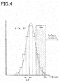
- Fig. 4 is an explanatory drawing of a remote Coulomb scattering calculation model.
- the spacer layer that is, the distance from the interface of the channel layer and the upper barrier layer to the planar doped layer is 3 nm
- the III-V group compound semiconductor spacer layer in which a V group element is Sb is 2 nm
- the remaining spacer layer is 1 nm.
- This configuration is compared with that in which the III-V group compound semiconductor spacer layer in which a V group element is Sb is not present and all 3 nm are taken by the composition same as that of the barrier layer.
- the calculation in this case is conducted under as assumption that the III-V group compound semiconductor spacer layer in which a V group element is Sb is AlSb and the remaining spacer layer is InAlAs.
- the total remote Coulomb force F total is a sum of Coulomb forces F(x) created by the donors present in regions divided by the width ⁇ x.
- x 0 denotes the position of the heterojunction interface
- e denotes an elementary charge
- ⁇ denotes a dielectric constant of the semiconductor
- the Coulomb forces appear to change significantly from the inverse proportionality to the square of the distance.
- the ratio of the Coulomb force F total(with AlSb) obtained when AlSb is introduced to the Coulomb force F total(without AlSb) obtained without the introduction of AlSb, that is, F total(with AlSb) /F total(without AlSb) is about 0.573, that is, reduces to about half. Therefore, it is clear that the remote Coulomb scattering can be suppressed.
- the thickness of the AlSb spacer layer is taken as 2.5 nm
- n total(with AlSb) /n total(without Al5b) is about 0.754
- F total(with Alsb) /F total(without AlSb) is about 0.410 and the Coulomb force is small, but the channel electron concentration decreases significantly. Therefore, it is desirable that the thickness of the III-V compound semiconductor spacer layer be 50% to 80% of the thickness between the channel layer/upper barrier layer interface and the planar doped layer.
- Another advantage is that since the energy at the conduction band edge of AlSb is higher than that of InAlAs as a barrier, quantum-mechanical penetration of channel electrons into the barrier layer or the real spatial transition between the upper barrier layer and channel layer can be suppressed.
- the lattice constant of AlSb is significantly different from that of other layers, but when it is used as a spacer layer, a thickness of about 2 nm to 2.5 nm is sufficient. Therefore, strained AlSb can be grown without the degradation of crystal quality.
- the planar doped layer is provided in one location in the upper barrier layer, but it may be also provided in the lower barrier layer or in the upper and lower barrier layers. Further, the planar doped layer may be provided in two or more locations in the same barrier layer, rather than in one location. When the planar doped layer is provided in two or more locations in the same barrier layer, the distance between the planar doped layers is set to 2 nm to 3 nm.
- the semiconductor substrate 1 is a semi-insulating InP substrate, semi-insulating GaAs substrate, or Si substrate.
- an InP HEMT an InAlAs/InGaAs heterostructure is formed on the semi-insulating InP substrate, semi-insulating GaAs substrate, or Si substrate.
- the buffer layer 2 can use In 0.52 Al 0.48 As same as in the lower barrier layer 3.
- the heterostructure when the heterostructure is formed on the semi-insulating GaAs substrate or Si substrate, using a composition-graded semiconductor layer (in this case, the lattice constant is made to increase gradually) as the buffer layer 2 and forming the layer such that the lattice constant of the uppermost portion of the buffer layer 2 matches the lattice constant of the In 0.52 Al 0.48 As lower barrier layer 3 are needed.
- a composition-graded semiconductor layer in this case, the lattice constant is made to increase gradually
- the buffer layer 2 In the case of a GaAs HEMT, an AlGaAs/(In)GaAs heterostructure is formed on the semi-insulating GaAs substrate or Si substrate.
- the buffer layer 2 can use AlGaAs same as in the lower barrier layer 3.
- the heterostructure is formed on the Si substrate, using a composition-graded semiconductor layer (in this case, the lattice constant is made to increase gradually) as the buffer layer 2 and forming the layer such that the lattice constant of the uppermost portion of the buffer layer 2 matches the lattice constant of the AlGaAs lower barrier layer 3 are needed.
- a composition-graded semiconductor layer in this case, the lattice constant is made to increase gradually
- the lower barrier layer 3 is an InAlAs layer
- the channel layer 4 is an InGaAs layer or a laminated structure of an InGaAs layer and an InAs layer.
- a portion of the upper barrier layer 5 other than the III-V compound semiconductor spacer layer 6 is an InAlAs layer or a laminated structure of an InAlAs layer and an InP layer.
- the cap layer 10 is an n-type InGaAs layer or a laminated structure of an n-type InGaAs layer and an n-type InAlAs layer.
- the lower barrier layer 3 is an AlGaAs layer
- the channel layer 4 is a GaAs layer or an InGaAs layer
- a portion of the upper barrier layer 5 other than the III-V compound semiconductor spacer layer 6 is an AlGaAs layer
- the cap layer 10 is an n-type GaAs layer.
- the III-V compound semiconductor spacer layer is any one of the AlSb layer, AlGaSb layer, AlInSb layer, and AlGaInSb layer.
- a GaSb layer is conductive, but when the Ga composition ratio is small, no problem is associated with the AlGaSb layer or AlGaInSb layer.
- An insulating film may be provided on the exposed flat surface of the cap layer, and the foot portion of the gate electrode can be supported by causing the side end surface of the opening provided in the insulating film to abut against the side end surface of the gate electrode.
- a very thin layer of AlSb in which Si is ionized and does not become a donor is provided in the spacer portion in the barrier layer. Therefore, where the electron concentration in the channel layer is to be increased by increasing Si- ⁇ doping which provides an electron supply layer, even though Si diffuses close to the channel layer in the spacer layer, it does not become the remote Coulomb scattering source and the electron mobility in the channel layer does not decrease.
- Fig.5 is a schematic cross-sectional view of the HEMT of Example 1 of the present invention.
- an i-type In 0.52 Al 0.48 As buffer layer 22 an i-type In 0.52 Al 0.48 As lower barrier layer 23, and an i-type InGaAs channel layer 24 are successively deposited on a semi-insulating InP substrate 21.
- an i-type AlSb spacer layer 25 and an i-type In 0.52 Al 0.48 As spacer layer 26 are successively deposited, and a ⁇ doped layer 27 is thereafter formed by ⁇ doping of Si.
- an i-type In 0.52 Al 0.48 As barrier layer 28 and an i-type InP layer 29 are successively deposited.
- the i-type AlSb spacer layer 25 through the i-type InP layer 29 constitute the upper barrier layer.
- the i-type InP layer 29 is provided to prevent the exposure of the i-type In 0.52 Al 0.48 As barrier layer 28 which is an Al-containing layer.
- a source electrode 31 and a drain electrode 32 are provided, with an n-type InGaAs cap layer 30 being provided therebelow.
- a gate electrode 41 is provided in a gate recess portion 40.
- Example 1 of the present invention the i-type AlSb spacer layer in which Si is ionized and does not become a donor is provided at the interface with the i-type InGaAs channel layer 24. Therefore, the effect of remote Coulomb scattering can be greatly reduced.
- the i-type In 0.52 Al 0.48 As buffer layer 22 with a thickness of 1000 nm, the i-type In 0.52 Al 0.48 As layer lower barrier layer 23 with a thickness of 200 nm, and the i-type InGaAs channel layer 24 with a thickness of 10 nm are deposited by the MBE method on the semi-insulating InP substrate 21.
- the i-type AlSb spacer layer 25 with a thickness of 2 nm and the i-type In 0.52 Al 0.48 As spacer layer 26 with a thickness of 1 nm are deposited.
- the ⁇ doped layer 27 is formed by using a cell containing a solid Si source and performing ⁇ doping of Si.
- the ⁇ doping amount of Si is taken as 1 ⁇ 10 13 cm -2 .
- the i-type In 0.52 Al 0.48 As barrier layer 28 with a thickness of 6 nm, the i-type InP layer 29 with a thickness of 3 nm, and the n-type InGaAs cap layer 30 with a thickness of 20 nm are deposited.
- the composition of the i-type InGaAs channel layer 24 is In x Ga 1-x As (0.8 ⁇ x ⁇ 0.53), and the composition of the n-type InGaAs cap layer 30 is In 0.53 Ga 0.47 As.
- the time of the growth process after the ⁇ doping is about 3 min.
- the impurity concentration in the n-type InGaAs cap layer 30 is 2 ⁇ 10 19 cm -3 .
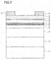
- the laminated structure provided on the wafer is divided into element regions, and the source electrode 31 and the drain electrode 32 are thereafter formed by depositing metal electrodes constituted by a Ti/Pt/Au laminated structure on the n-type InGaAs cap layer 30, as illustrated in Fig. 7 .
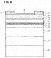
- a SiO 2 film 33 with a thickness of 20 nm is formed on the n-type InGaAs cap layer 30 between the source electrode 31 and the drain electrode 32 by using a plasma CVD method.
- a first resist layer 34 is formed on the SiO 2 film 33 in the recess portion between the source electrode 31 and the drain electrode 32, and a second resist layer 35 and a third resist layer 36 are formed on the first resist layer.
- an electron beam resist ZEP (trade name, ZEON CORPORATION) is used as the first resist layer 34 and the third resist layer 36.
- PMGI Poly-dimethylglutarimide: manufactured by MicroChem Corp., trade name
- the thickness of the first resist layer 34 changes depending on the length of the foot portion of the gate electrode. For this reason, in Figs.
- the thickness of the first resist layer 34 represents the uppermost portion of the metal used for the source electrode 31 and the drain electrode 32, but the thickness can be larger or smaller than this.
- the first resist layer 34 covers both the source electrode 31 and the drain electrode 32.
- the second resist layer 35 penetrates between the source electrode 31 and the drain electrode 32.
- the head portion of the T-shaped gate electrode is exposed by the electron beam exposure method and an opening 37 is formed by developing the third resist layer 36 and the second resist layer 35.
- highly accurate exposure of the first resist layer 34 is further performed by the electron beam exposure method to match the target gate length, and an opening 38 corresponding to the foot portion of the T-shaped gate electrode is formed.
- an opening 39 is formed by removing the exposed portion of the SiO 2 film 33 by reactive ion etching by using the first resist layer 34, in which the opening 38 has been formed, as a mask.
- CF 4 is used as the etching gas.
- the n-type InGaAs cap layer 30 is etched by performing wet etching using the SiO 2 film 33, in which the opening 39 has been formed, as a mask, thereby forming a gate recess portion 40 and electrically separating the n-type InGaAs cap layer 30.
- a mixed solution of citric acid (C 6 H 8 O 7 ) and hydrogen peroxide (H 2 O 2 ) is used as the etching solution.
- a Ti/Pt/Au laminated film is vapor deposited as a gate electrode 41.
- layers from the third resist layer 36 through the first resist layer 34 are removed and the Ti/Pt/Au laminated film deposited on the third resist layer 36 is also removed by lift-off, thereby producing the basic structure of the HEMT of Example 1 of the present invention.
- Fig. 16 is a schematic cross-sectional view of the HEMT of Example 2 of the present invention.
- the i-type In 0.52 Al 0.48 AS buffer layer 22, the i-type In 0.52 Al 0.48 As lower barrier layer 23, and the i-type InGaAs channel layer 24 are successively deposited on the semi-insulating InP substrate 21.
- the i-type AlSb spacer layer 25 and the i-type In 0.52 Al 0.48 As spacer layer 26 are successively deposited, and the ⁇ doped layer 27 is thereafter formed by ⁇ doping of Si.
- the i-type In 0.52 Al 0.48 As spacer layer 42 with a thickness of 2 nm is deposited and then the ⁇ doped layer 43 is formed by again performing the Si- ⁇ doping to about 1 ⁇ 10 13 cm -2 .
- the i-type In 0.52 Al 0.48 AS barrier layer 28 and the i-type InP layer 29 are successively deposited in the same manner as in Example 1.
- the layers from the i-type AlSb spacer layer 25 through the i-type InP layer 29 constitute the upper barrier layer.
- the source electrode 31 and the drain electrode 32 are provided, with the n-type InGaAs cap layer 30 being provided therebelow.
- the gate electrode 41 is provided in the gate recess portion 40.
- Example 2 of the present invention the i-type AlSb spacer layer is provided at the interface with the i-type InGaAs channel layer 24. Therefore, although two ⁇ doped layers are provided and the carrier supply capacity is increased, the effect of remote Coulomb scattering can be greatly reduced.
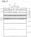
- Fig. 17 is a schematic cross-sectional view of the HEMT of Example 3 of the present invention. As illustrated in the figure, the i-type In 0.52 Al 0.48 As buffer layer 22 and the i-type In 0.52 Al 0.48 As lower barrier layer 23 are successively deposited on the semi-insulating InP substrate 21.
- a ⁇ doped layer 44 is formed by performing the Si- ⁇ doping to about 1 ⁇ 10 13 cm -2 , and an i-type In 0.52 Al 0.48 As spacer layer with a thickness of 1 nm and an i-type AlSb spacer layer 46 with a thickness of 2 nm are thereafter formed.
- the i-type InGaAs channel layer 24, i-type AlSb spacer layer 25, and i-type In 0.52 Al 0.48 As spacer layer 26 are then successively formed and the ⁇ doped layer 27 is formed by ⁇ doping of Si in the same manner as in Example 1.
- the i-type In 0.52 Al 0.48 As barrier layer 28 and the i-type InP layer 29 are successively deposited.
- the source electrode 31 and the drain electrode 32 are then provided, with the n-type InGaAs cap layer 30 being provided therebelow.
- the gate electrode 41 is provided in the gate recess portion 40.
- Example 3 of the present invention the carrier supply capacity is increased by providing the ⁇ doped layer in the upper and lower barrier layers, but because the AlSb spacer layer is provided on the interfaces of the upper and lower barrier layers with the channel layer, the effect of remote Coulomb scattering can be greatly reduced.
- Fig. 18 is a schematic cross-sectional view of the HEMT of Example 4 of the present invention. As illustrated in the figure, the i-type In 0.52 Al 0.48 As buffer layer 22 and the i-type In 0.52 Al 0.48 As lower barrier layer 23 are successively deposited on the semi-insulating InP substrate 21.
- a ⁇ doped layer 44 is formed by performing the Si- ⁇ doping to about 1 ⁇ 10 13 cm -2 , and the i-type In 0.52 Al 0.48 AS spacer layer 45 with a thickness of 1 nm and the i-type AlSb spacer layer 46 with a thickness of 2 nm are thereafter formed.
- the i-type InGaAs channel layer 24, the i-type In 0.52 Al 0.48 As barrier layer 28 and the i-type InP layer 29 are then successively deposited.
- the source electrode 31 and the drain electrode 32 are then provided, with the n-type InGaAs cap layer 30 being provided therebelow.
- the gate electrode 41 is provided in the gate recess portion 40.
- Example 4 of the present invention the ⁇ doped layer is provided in the lower barrier layer, but because the AlSb spacer layer is provided on the interface of the lower barrier layer with the channel layer, the effect of remote Coulomb scattering can be greatly reduced.
- Fig. 19 is a schematic cross-sectional view of the HEMT of Example 5 of the present invention. As illustrated in the figure, the i-type In 0.52 Al 0.48 AS buffer layer 22 and the i-type In 0.52 Al 0.48 As lower barrier layer 23 are successively deposited on the semi-insulating InP substrate 21.
- a ⁇ doped layer 47 is formed by performing the Si- ⁇ doping to about 1 ⁇ 10 13 cm -2 , and then the i-type In 0.52 Al 0.48 As spacer layer 48 with a thickness of 2 nm is formed.
- the ⁇ doped layer 44 is then formed by again performing the Si- ⁇ doping to about 1 ⁇ 10 13 cm -2 , and the i-type In 0.52 Al 0.48 As spacer layer 45 with a thickness of 1 nm and the i-type AlSb spacer layer 46 with a thickness of 2 nm are thereafter formed.
- the i-type InGaAs channel layer 24, the i-type AlSb spacer layer 25, and the i-type In 0.52 Al 0.48 As spacer layer 26 are then successively deposited, and the ⁇ doped layer 27 is then formed by ⁇ doping of Si.
- the i-type In 0.52 Al 0.48 As spacer layer 42 with a thickness of 2 nm is then deposited, and the ⁇ doped layer 43 is then formed by again performing the Si- ⁇ doping to about 1 ⁇ 10 13 cm -2 .
- the i-type In 0.52 Al 0.48 As spacer barrier 28 and the i-type InP layer 29 are then successively deposited in the same manner as in Example 1.
- the source electrode 31 and the drain electrode 32 are then provided, with the n-type InGaAs cap layer 30 being provided therebelow.
- the gate electrode 41 is provided in the gate recess portion 40.
- Example 5 of the present invention the carrier supply capacity is further increased by providing two ⁇ doped layers in the upper and lower barrier layers, but because the AlSb spacer layer is provided on the interfaces of the upper and lower barrier layers with the channel layer, the effect of remote Coulomb scattering can be greatly reduced.
- Fig. 20 is a schematic cross-sectional view of the HEMT of Example 6 of the present invention. As illustrated in the figure, the i-type In 0.52 Al 0.48 As buffer layer 22 and the i-type In 0.52 Al 0.48 As lower barrier layer 23 are successively deposited on the semi-insulating InP substrate 21.
- the ⁇ doped layer 47 is formed by performing the Si- ⁇ doping to about 1 ⁇ 10 13 cm -2 , and then the i-type In 0.52 Al 0.48 As spacer layer 48 with a thickness of 2 nm is formed.
- the ⁇ doped layer 44 is then formed by again performing the Si- ⁇ doping to about 1 ⁇ 10 13 cm -2 , and the i-type In 0.52 Al 0.48 As spacer layer 45 with a thickness of 1 nm and the i-type AlSb spacer layer 46 with a thickness of 2 nm are thereafter formed.
- the i-type InGaAs channel layer 24, the i-type In 0.52 Al 0.48 AS spacer barrier 28, and the i-type InP layer 29 are then successively deposited.
- the source electrode 31 and the drain electrode 32 are then provided, with the n-type InGaAs cap layer 30 being provided therebelow.
- the gate electrode 41 is provided in the gate recess 40.
- Example 6 of the present invention the carrier supply capacity is increased by providing two 5 doped layers in the lower barrier layer, but because the AlSb spacer layer is provided on the interface of the lower barrier layer with the channel layer, the effect of remote Coulomb scattering can be greatly reduced.
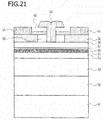
- the HEMT of Example 7 of the present invention will be explained hereinbelow with reference to Fig. 21 .
- the HEMT of Example 7 is a GaAs HEMT with a GaAs substrate.
- the basic configuration thereof is the same as in Example 1.
- Fig. 21 is a schematic cross-sectional view of the HEMT of Example 7 of the present invention. As illustrated in the figure, and i-type AlGaAs buffer layer 52 with a thickness of 1000 nm and an i-type AlGaAs lower barrier layer 53 with a thickness of 200 nm are successively deposited on a semi-insulating GaAs substrate 51.
- an i-type InGaAs channel layer 54 with a thickness of 10 nm, an i-type AlSb spacer layer 55 with a thickness of 2 nm, and an i-type AlGaAs spacer layer 56 with a thickness of 1 nm are successively deposited, and a ⁇ doped layer 57 is formed by ⁇ doping of Si.
- An i-type AlGaAs buffer layer 58 with a thickness of 6 nm and an n-type GaAs cap layer 59 with an impurity concentration of 2 ⁇ 10 19 cm -3 and a thickness of 20 nm are then deposited.
- a source electrode 60 and a drain electrode 61 are then provided, with an n-type GaAs cap layer 59 being provided therebelow.
- a gate electrode 64 is provided in the gate recess 63.
- a SiO 2 film 62 is also provided on the exposed flat surface of an n-type GaAs cap layer 59.
- Example 7 of the present invention a GaAs HEMT is provided in which the substrate is from GaAs, but the circumstances of remote Coulomb diffusion which follows the increase in impurity concentration in the ⁇ doped layer are the same as in the InP HEMT.
- the AlSb spacer layer is provided on the interface of the AlGaAs barrier layer, which has been provided with the ⁇ doped layer, with the channel layer, the effect of remote Coulomb scattering can be greatly reduced.
- the ⁇ doped layer is provided only on the upper barrier layer side, as in the above-described Example 1.
- the ⁇ doped layer may be also provided in the lower barrier layer or the upper and lower barrier layers, or a plurality of ⁇ doped layers may be provided in the same barrier layer in the same manner as in Examples 2 to 6.
- the channel layer is from InGaAs, but GaAs may be also used therefor.
Landscapes
- Junction Field-Effect Transistors (AREA)
Abstract
Description
- The present invention relates to a field-effect compound semiconductor device such as a high-electron-mobility transistor (HEMT) which is a high-speed transistor.
- High-electron-mobility transistors (HEMTs) using III-V group compound semiconductors are high-speed transistors capable of operating in a milliwave (30 GHz to 300 GHz) to sub-milliwave (300 GHz to 3 THz) range. Among them, InP HEMTs using an InAlAs/InGaAs junction structure are field-effect transistors which presently have the world's highest speed at a cut-off frequency fT = 688 GHz (see, for example, Non-Patent Literature 1).
- The cut-off frequency fT, which is one of the indicators of high speed ability of the HEMTs, can be represented as

- However, the ratio of the parasitic delay time τex in the total delay time has recently become relatively large due to a significant decrease in the intrinsic delay time, and the decrease in the parasitic delay time has also become an important problem in terms of speed increase.
- The effect of source resistance or drain resistance is one of the factors contributing to the parasitic delay time τex. The source (drain) resistance is constituted by an ohmic contact resistance and sheet resistance of the channel layer. Among them, the sheet resistance can be reduced by increasing the electron density in the channel layer. Accordingly, an attempt has been made to increase the Si-δ doping amount in the InAlAs electron supply layer above the InGaAs channel layer.
- High-concentration doping of 1 × 1013 cm-2 or higher is presently performed as the Si-δ doping. An InP HEMT will be explained hereinbelow with reference to
Fig. 22. Fig. 22 is a schematic cross-sectional view of the conventional InP HEMT. As illustrated in the figure, an i-type In0.52Al0.48Asbuffer layer 72, an i-type In0.52Al0.48Aslower barrier layer 73, an i-typeInGaAs channel layer 74, and an i-type In0.52Al0.48Asspacer layer 75 are successively deposited on asemi-insulating InP substrate 71. - Then, a δ doped
layer 76 is formed by δ doping Si, and an i-type In-0.52Al0.48Asbarrier layer 77 and an i-type InP layer 78 are thereafter successively deposited. Those i-type In0.52Al0.48Asspacer layer 75 through the i-type InP layer 78 serve as an upper barrier layer. The i-type InP layer is provided to prevent the exposure of the i-type In0.52Al0.48Asbarrier layer 77 which is an Al-containing layer. Then, asource electrode 80 and adrain electrode 81 are provided, with an n-typeInGaAs cap layer 79 being located therebelow. Agate electrode 83 is provided in agate recess portion 82. - The sheet resistance Rsheet of the HEMT can be represented as

Figs. 23A and 23B . -
Figs. 23A and 23B is an explanatory drawing illustrating the distribution of Si after δ doping,Fig. 23A is the distribution diagram in the case of low-concentration 5 doping, andFig. 23B is the distribution diagram in the case of high-concentration δ doping. As illustrated inFig. 23A , Si introduced by δ doping does not remain "as is" at the initial doping position. Since the growth of the barrier layer or cap layer is performed at a high temperature after the Si-δ doping, the Si which had a substantially δ-function distribution immediately after the doping diffuses up and down in the thickness direction of the grown layer. - Even when the growth temperature or growth time is the same, where the Si-δ doping concentration is high, Si diffuses closer to the channel layer, as illustrated in
Fig. 23B . Si which is a donor is ionized and, even while remaining in the spacer layer, exerts a Coulomb force to the electrons in the channel layer and causes the remote Coulomb scattering. In particular, since the Coulomb force is inversely proportional to the square of the distance, where the scattering source present in the upper barrier layer approaches the channel layer, the channel electron mobility is greatly reduced and the sheet resistance increases. - The Si-δ doping method can also have another configuration. In the aforementioned
Non-Patent Literature 1 describing how the world's highest speed has been achieved, Si-δ doping, which is the source of electron supply to the channel layer, is provided in two locations in the InAlAs barrier layer. With such a method, it is possible to increase the electron concentration in the channel layer and reduce the sheet resistance. - However, since the Si doping amount is increased, the diffusion of Si in the channel layer direction in the crystal growth or processing increases over that in the case of a single location of Si-δ doping. This is because the diffusion of Si in the up-down direction becomes asymmetric due to Si-δ doping in two locations. In particular, with the Si-δ doping close to the channel, the diffusion in the channel direction is large, whereas the diffusion in the opposite direction is small.
- Si is prevented from diffusing into the channel layer by providing the spacer layer. However, since the amount of Si at a position close to the channel layer increases, the effect of remote Coulomb scattering is enhanced and the electron mobility in the channel layer decreases. For this reason, since the electron mobility µ decreases even when the electron concentration Ns is increased by the double Si-δ doping, the double doping fails to reduce the resistance by half.
- Meanwhile, a double doped structure is also known in which Si-δ doping has been performed above and below an InGaAs channel layer in order to increase the electron concentration in the channel layer. In a HEMT using such a structure the cut-off frequency fT is reported to be 660 GHz (see, for example, Non-Patent Literature 2). However, in this structure, the diffusion of Si-δ doping in the lower barrier layer is larger than the diffusion of Si-δ doping in the upper barrier layer. As a result, the channel electron concentration is difficult to increase while suppressing the effect of Si diffusion.
-
- Non-Patent Literature 1: Kim et al., IEDM Tech. Dig., no. 13.6, Dec. 2011
- Non-Patent Literature 2: Leuther et al., Proc. 23rd IPRM, no. Tu-4. 2. 2, p. 295, May 2011
- Non-Patent Literature 3: M. E. Greiner and J. F. Gibbonset, Appl. Phys. Lett. Vol. 44, p. 750, 1984
- As mentioned hereinabove, because of high-concentration δ doping of Si, the diffusion of Si increases and the ionized Si comes closer to the channel layer. As a result, the remote Coulomb scattering caused by the ionized Si in the barrier layer increases. Since the Coulomb force is inversely proportional to the square of the distance, the ionized Si which has approached the channel layer demonstrates a prominent effect, and the remote Coulomb scattering causes the decrease in the channel electron mobility. The resultant problem is that sheet resistance increases and does not decrease as expected.
- Thus, it is an objective to reduce the sheet resistance which is due to high-concentration δ doping and also to reduce the remote Coulomb scattering in a field-effect compound semiconductor device.
- A field-effect compound semiconductor device comprising:
- a semiconductor substrate;
- a lower barrier layer that is provided on the semiconductor substrate;
- a channel layer that is provided in contact with the lower barrier layer;
- an upper barrier layer that is provided in contact with the channel layer;
- a cap layer that is provided in contact with the upper barrier layer;
- a source electrode and a drain electrode that are provided on the cap layer; and
- a gate electrode that is arranged between the source electrode and the drain electrode, wherein
- a planar doped layer that is planarly doped with impurity atoms, which are to be a channel electron supply source, is provided in at least one of the lower barrier layer and the upper barrier layer; and
- a portion of the barrier layer, where the planar doped layer has been provided, is a III-V group compound semiconductor spacer layer in which a V group element is Sb, with this portion being in contact with the channel layer.
- In the disclosed field-effect compound semiconductor device, both the reduction in the sheet resistance, which is due to high-concentration δ doping, and the reduction in the remote Coulomb scattering can be achieved.
-
-
Fig. 1 is a schematic cross-sectional view of a field-effect compound semiconductor device of an embodiment of the present invention. -
Fig. 2 is an explanatory drawing of an impurity diffusion model. -
Fig. 3 is an explanatory drawing of impurity diffusion calculation results. -
Fig. 4 is an explanatory drawing of a remote Coulomb scattering calculation model. -
Fig. 5 is a schematic cross-sectional view of the HEMT of Example 1 of the present invention. -
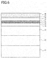
Fig. 6 is an explanatory drawing illustrating first part of the process for manufacturing the HEMT of Example 1 of the present invention. -
Fig. 7 is an explanatory drawing illustrating first part of the process for manufacturing the HEMT of Example 1 of the present invention after the process illustrated byFig. 6 . -
Fig. 8 is an explanatory drawing illustrating first part of the process for manufacturing the HEMT of Example 1 of the present invention after the process illustrated byFig. 7 . -
Fig. 9 is an explanatory drawing illustrating first part of the process for manufacturing the HEMT of Example 1 of the present invention after the process illustrated byFig. 8 . -
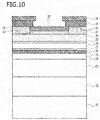
Fig. 10 is an explanatory drawing illustrating first part of the process for manufacturing the HEMT of Example 1 of the present invention after the process illustrated byFig. 9 . -
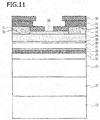
Fig. 11 is an explanatory drawing illustrating first part of the process for manufacturing the HEMT of Example 1 of the present invention after the process illustrated byFig. 10 . -
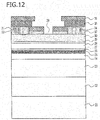
Fig. 12 is an explanatory drawing illustrating first part of the process for manufacturing the HEMT of Example 1 of the present invention after the process illustrated byFig. 11 . -
Fig. 13 is an explanatory drawing illustrating first part of the process for manufacturing the HEMT of Example 1 of the present invention after the process illustrated byFig. 12 . -
Fig. 14 is an explanatory drawing illustrating first part of the process for manufacturing the HEMT of Example 1 of the present invention after the process illustrated byFig. 13 . -
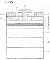
Fig. 15 is an explanatory drawing illustrating first part of the process for manufacturing the HEMT of Example 1 of the present invention after the process illustrated byFig. 14 . -
Fig. 16 is a schematic cross-sectional view of the HEMT of Example 2 of the present invention. -
Fig. 17 is a schematic cross-sectional view of the HEMT of Example 3 of the present invention. -
Fig. 18 is a schematic cross-sectional view of the HEMT of Example 4 of the present invention. -
Fig. 19 is a schematic cross-sectional view of the HEMT of Example 5 of the present invention. -
Fig. 20 is a schematic cross-sectional view of the HEMT of Example 6 of the present invention. -
Fig. 21 is a schematic cross-sectional view of the HEMT of Example 7 of the present invention. -
Fig. 22 is a schematic cross-sectional view of the conventional HEMT. -
Fig. 23A and Fig.23B are is schematic diagrams illustrating the diffusion of impurities. - The field-effect compound semiconductor devices of the embodiments of the present invention will be described hereinbelow with reference to
Figs. 1 to 4 .Fig. 1 is a schematic cross-sectional view of a field-effect compound semiconductor device of an embodiment of the present invention. As illustrated in the figure, abuffer layer 2, alower barrier layer 3, and achannel layer 4 are successively formed on asemiconductor substrate 1. Then, a III-V group compoundsemiconductor spacer layer 6 in which a V group element is Sb and aspacer layer 7 are successively deposited, a planar dopedlayer 8 is thereafter formed by δ doping of Si, and then abarrier layer 9 is formed. Layers from the III-V group compoundsemiconductor spacer layer 6 through thebarrier layer 9 constitute anupper barrier layer 5. Then, asource electrode 11 and adrain electrode 12 are provided, with acap layer 10 being disposed therebelow, and agate electrode 13 is provided in a gate recess portion. When thelower barrier layer 3 is lattice matched to thesemiconductor substrate 1, thebuffer layer 2 and thelower barrier layer 3 become the same semiconductor layer. However when the lattices are not matched, using a composition-graded semiconductor layer as thebuffer layer 2 and forming the layer such that the lattice constant of the uppermost portion of thebuffer layer 2 matches the lattice constant of thelower barrier layer 3 are needed. A molecular beam epitaxy (MBE) method is typically used for layer deposition, but a metalorganic vapor phase epitaxy method (MOVPE) may be also used. - Since Si does not act as a donor in the III-V group compound
semiconductor spacer layer 6 in which a V group element is Sb, the ionized Si which causes the remote Coulomb scattering is not present in the III-V group compoundsemiconductor spacer layer 6. Therefore, the decrease in channel electron mobility caused by the remote Coulomb scattering can be suppressed. Incidentally, in the III-V group compound semiconductor in which a V group element is Sb, Te is used as a donor impurity. -
Fig. 2 is an explanatory drawing of an impurity diffusion model. The rectangle in the figure illustrates the state in which an impurity is δ doped at a concentration of no in a range with a position x in the lamination direction from -L to +L, that is, the state with (Dt)1/2 = 0. Here D is the diffusion coefficient of the impurity, t is a heat treatment time, that is, the period of time in which crystal growth is performed on the planar doped layer, and (Dt)1/2 is a diffusion length. - The impurity concentration distribution n(x, t) after the diffusion caused by the heat treatment is represented as:


- In the fabrication of an InP HEMT, the crystal growth is performed at about 480°C to 540°C, and the growth time after Si-δ doping is 2 min to 3 min. Under such conditions, the diffusion length is about (Dt)1/2 = 0.5 nm (see, for example, Non-Patent Literature 3).
-
Fig. 3 is an explanatory drawing of impurity diffusion calculation results. The calculations were performed with respect to combinations of three temperature conditions, namely, 500°C, 520°C, and 540°C, and two growth times of 2 min and 3 min. In this case, L is about 0.3 nm where the Si-δ doping amount is taken as 1 × 1013 cm-2, Si is assumed to be δ doped within ±1 monolayer from the center, and the unevenness of an underlayer is taken to be of one monolayer. Therefore, n0 = 1.66 × 1020 cm-3.Fig. 3 illustrates the results obtained by calculating the distribution of Si from Expressions (3) and (4) above by using the aforementioned numerical values. In the case of an average temperature of 520°C and a time of 3 min, (Dt)1/2 = 0.5 nm. -
Fig. 4 is an explanatory drawing of a remote Coulomb scattering calculation model. In the mode, the spacer layer, that is, the distance from the interface of the channel layer and the upper barrier layer to the planar doped layer is 3 nm, the III-V group compound semiconductor spacer layer in which a V group element is Sb is 2 nm, and the remaining spacer layer is 1 nm. This configuration is compared with that in which the III-V group compound semiconductor spacer layer in which a V group element is Sb is not present and all 3 nm are taken by the composition same as that of the barrier layer. The calculation in this case is conducted under as assumption that the III-V group compound semiconductor spacer layer in which a V group element is Sb is AlSb and the remaining spacer layer is InAlAs. - In the calculation, the Coulomb force received by electrons on the channel layer/AlSb heterojunction interface from the ionized donor at each position x is integrated. Therefore, the total remote Coulomb force Ftotal is a sum of Coulomb forces F(x) created by the donors present in regions divided by the width Δx. Where x0 denotes the position of the heterojunction interface, e denotes an elementary charge, and ε denotes a dielectric constant of the semiconductor,

- In the case of 520°C, 3 min, and (Dt)1/2 = 0.5 nm, the ratio of the electron concentration ntotal(with AlSb) obtained when AlSb is introduced to the electron concentration ntotal(without AlSb) obtained without the introduction of AlSb, that is, ntotal(with AlSb)/ntotal(without AlSb), is about 0.914. It is clear that the reduction in the number of channel electrons caused by the introduction of AlSb is 10% or less.
- As for the ratio of Coulomb forces which are created by ionized donors and received by channel electrons, where the ionized donor distribution is taken into account, the Coulomb forces appear to change significantly from the inverse proportionality to the square of the distance. The ratio of the Coulomb force Ftotal(with AlSb) obtained when AlSb is introduced to the Coulomb force Ftotal(without AlSb) obtained without the introduction of AlSb, that is, Ftotal(with AlSb)/Ftotal(without AlSb), is about 0.573, that is, reduces to about half. Therefore, it is clear that the remote Coulomb scattering can be suppressed.
- Incidentally, where the thickness of the AlSb spacer layer is taken as 2.5 nm, ntotal(with AlSb)/ntotal(without Al5b) is about 0.754 and Ftotal(with Alsb)/Ftotal(without AlSb) is about 0.410 and the Coulomb force is small, but the channel electron concentration decreases significantly. Therefore, it is desirable that the thickness of the III-V compound semiconductor spacer layer be 50% to 80% of the thickness between the channel layer/upper barrier layer interface and the planar doped layer.
- Another advantage is that since the energy at the conduction band edge of AlSb is higher than that of InAlAs as a barrier, quantum-mechanical penetration of channel electrons into the barrier layer or the real spatial transition between the upper barrier layer and channel layer can be suppressed. The lattice constant of AlSb is significantly different from that of other layers, but when it is used as a spacer layer, a thickness of about 2 nm to 2.5 nm is sufficient. Therefore, strained AlSb can be grown without the degradation of crystal quality.
- In the above-descried embodiment, the planar doped layer is provided in one location in the upper barrier layer, but it may be also provided in the lower barrier layer or in the upper and lower barrier layers. Further, the planar doped layer may be provided in two or more locations in the same barrier layer, rather than in one location. When the planar doped layer is provided in two or more locations in the same barrier layer, the distance between the planar doped layers is set to 2 nm to 3 nm.
- As a specific structure, the
semiconductor substrate 1 is a semi-insulating InP substrate, semi-insulating GaAs substrate, or Si substrate. In the case of an InP HEMT, an InAlAs/InGaAs heterostructure is formed on the semi-insulating InP substrate, semi-insulating GaAs substrate, or Si substrate. When the heterostructure is formed on the semi-insulating InP substrate, thebuffer layer 2 can use In0.52Al0.48As same as in thelower barrier layer 3. By contrast, when the heterostructure is formed on the semi-insulating GaAs substrate or Si substrate, using a composition-graded semiconductor layer (in this case, the lattice constant is made to increase gradually) as thebuffer layer 2 and forming the layer such that the lattice constant of the uppermost portion of thebuffer layer 2 matches the lattice constant of the In0.52Al0.48Aslower barrier layer 3 are needed. In the case of a GaAs HEMT, an AlGaAs/(In)GaAs heterostructure is formed on the semi-insulating GaAs substrate or Si substrate. When the heterostructure is formed on the semi-insulating GaAs substrate, thebuffer layer 2 can use AlGaAs same as in thelower barrier layer 3. By contrast, when the heterostructure is formed on the Si substrate, using a composition-graded semiconductor layer (in this case, the lattice constant is made to increase gradually) as thebuffer layer 2 and forming the layer such that the lattice constant of the uppermost portion of thebuffer layer 2 matches the lattice constant of the AlGaAslower barrier layer 3 are needed. There are a great variety of buffer layer structures, and the structure of this layer cannot be uniquely defined. - When a semi-insulating InP substrate is used, the
lower barrier layer 3 is an InAlAs layer, and thechannel layer 4 is an InGaAs layer or a laminated structure of an InGaAs layer and an InAs layer. Further, a portion of theupper barrier layer 5 other than the III-V compoundsemiconductor spacer layer 6 is an InAlAs layer or a laminated structure of an InAlAs layer and an InP layer. Thecap layer 10 is an n-type InGaAs layer or a laminated structure of an n-type InGaAs layer and an n-type InAlAs layer. - When a semi-insulating GaAs substrate is used, the
lower barrier layer 3 is an AlGaAs layer, and thechannel layer 4 is a GaAs layer or an InGaAs layer. A portion of theupper barrier layer 5 other than the III-V compoundsemiconductor spacer layer 6 is an AlGaAs layer, and thecap layer 10 is an n-type GaAs layer. - Further, the III-V compound semiconductor spacer layer is any one of the AlSb layer, AlGaSb layer, AlInSb layer, and AlGaInSb layer. A GaSb layer is conductive, but when the Ga composition ratio is small, no problem is associated with the AlGaSb layer or AlGaInSb layer.
- An insulating film may be provided on the exposed flat surface of the cap layer, and the foot portion of the gate electrode can be supported by causing the side end surface of the opening provided in the insulating film to abut against the side end surface of the gate electrode.
- In the embodiments of the present invention, a very thin layer of AlSb in which Si is ionized and does not become a donor is provided in the spacer portion in the barrier layer. Therefore, where the electron concentration in the channel layer is to be increased by increasing Si-δ doping which provides an electron supply layer, even though Si diffuses close to the channel layer in the spacer layer, it does not become the remote Coulomb scattering source and the electron mobility in the channel layer does not decrease.
- The HEMT of Example 1 of the present invention will be explained hereinbelow with reference to
Figs. 5 to 15 .Fig.5 is a schematic cross-sectional view of the HEMT of Example 1 of the present invention. As illustrated in the figure, an i-type In0.52Al0.48Asbuffer layer 22, an i-type In0.52Al0.48Aslower barrier layer 23, and an i-typeInGaAs channel layer 24 are successively deposited on asemi-insulating InP substrate 21. Then, an i-typeAlSb spacer layer 25 and an i-type In0.52Al0.48Asspacer layer 26 are successively deposited, and a δ dopedlayer 27 is thereafter formed by δ doping of Si. - Then, an i-type In0.52Al0.48As
barrier layer 28 and an i-type InP layer 29 are successively deposited. The i-typeAlSb spacer layer 25 through the i-type InP layer 29 constitute the upper barrier layer. The i-type InP layer 29 is provided to prevent the exposure of the i-type In0.52Al0.48Asbarrier layer 28 which is an Al-containing layer. Then, asource electrode 31 and adrain electrode 32 are provided, with an n-typeInGaAs cap layer 30 being provided therebelow. Agate electrode 41 is provided in agate recess portion 40. - Thus, in Example 1 of the present invention, the i-type AlSb spacer layer in which Si is ionized and does not become a donor is provided at the interface with the i-type
InGaAs channel layer 24. Therefore, the effect of remote Coulomb scattering can be greatly reduced. - A process for manufacturing the HEMT of Example 1 of the present invention will be explained hereinbelow with reference to
Figs. 6 to 15 . Initially, as illustrated inFig. 6 , the i-type In0.52Al0.48Asbuffer layer 22 with a thickness of 1000 nm, the i-type In0.52Al0.48As layerlower barrier layer 23 with a thickness of 200 nm, and the i-typeInGaAs channel layer 24 with a thickness of 10 nm are deposited by the MBE method on thesemi-insulating InP substrate 21. Then, the i-typeAlSb spacer layer 25 with a thickness of 2 nm and the i-type In0.52Al0.48Asspacer layer 26 with a thickness of 1 nm are deposited. - Then, the δ doped
layer 27 is formed by using a cell containing a solid Si source and performing δ doping of Si. The δ doping amount of Si is taken as 1 × 1013 cm-2. Then, the i-type In0.52Al0.48Asbarrier layer 28 with a thickness of 6 nm, the i-type InP layer 29 with a thickness of 3 nm, and the n-typeInGaAs cap layer 30 with a thickness of 20 nm are deposited. The composition of the i-typeInGaAs channel layer 24 is InxGa1-xAs (0.8 ≥ x ≥ 0.53), and the composition of the n-typeInGaAs cap layer 30 is In0.53Ga0.47As. The time of the growth process after the δ doping is about 3 min. The impurity concentration in the n-typeInGaAs cap layer 30 is 2 × 1019 cm-3. - Then, the laminated structure provided on the wafer is divided into element regions, and the
source electrode 31 and thedrain electrode 32 are thereafter formed by depositing metal electrodes constituted by a Ti/Pt/Au laminated structure on the n-typeInGaAs cap layer 30, as illustrated inFig. 7 . - Then, as illustrated in
Fig. 8 , a SiO2 film 33 with a thickness of 20 nm is formed on the n-typeInGaAs cap layer 30 between thesource electrode 31 and thedrain electrode 32 by using a plasma CVD method. - Then, as illustrated in
Fig. 9 , a first resistlayer 34 is formed on the SiO2 film 33 in the recess portion between thesource electrode 31 and thedrain electrode 32, and a second resistlayer 35 and a third resistlayer 36 are formed on the first resist layer. In this case, an electron beam resist ZEP (trade name, ZEON CORPORATION) is used as the first resistlayer 34 and the third resistlayer 36. Further, PMGI (Poly-dimethylglutarimide: manufactured by MicroChem Corp., trade name) is used as the second resistlayer 35. The thickness of the first resistlayer 34 changes depending on the length of the foot portion of the gate electrode. For this reason, inFigs. 9 to 14 , the thickness of the first resistlayer 34 represents the uppermost portion of the metal used for thesource electrode 31 and thedrain electrode 32, but the thickness can be larger or smaller than this. When the thickness is large, the first resistlayer 34 covers both thesource electrode 31 and thedrain electrode 32. When the thickness is small, the second resistlayer 35 penetrates between thesource electrode 31 and thedrain electrode 32. - Then, as illustrated in
Fig. 10 , the head portion of the T-shaped gate electrode is exposed by the electron beam exposure method and anopening 37 is formed by developing the third resistlayer 36 and the second resistlayer 35. Then, as illustrated inFig. 11 , highly accurate exposure of the first resistlayer 34 is further performed by the electron beam exposure method to match the target gate length, and anopening 38 corresponding to the foot portion of the T-shaped gate electrode is formed. - Then, as illustrated in
Fig. 12 , anopening 39 is formed by removing the exposed portion of the SiO2 film 33 by reactive ion etching by using the first resistlayer 34, in which theopening 38 has been formed, as a mask. CF4 is used as the etching gas. - Then, as illustrated in
Fig. 13 , the n-typeInGaAs cap layer 30 is etched by performing wet etching using the SiO2 film 33, in which theopening 39 has been formed, as a mask, thereby forming agate recess portion 40 and electrically separating the n-typeInGaAs cap layer 30. A mixed solution of citric acid (C6H8O7) and hydrogen peroxide (H2O2) is used as the etching solution. - Then, as illustrated in
Fig. 14 , a Ti/Pt/Au laminated film is vapor deposited as agate electrode 41. Then, as illustrated inFig. 15 , layers from the third resistlayer 36 through the first resistlayer 34 are removed and the Ti/Pt/Au laminated film deposited on the third resistlayer 36 is also removed by lift-off, thereby producing the basic structure of the HEMT of Example 1 of the present invention. - The HEMT of Example 2 of the present invention will be explained hereinbelow with reference to
Fig. 16 . In the HEMT of Example 2, Si-δ doping is performed twice in the upper barrier layer. Other features, namely, the thickness of the layers, impurity concentrations, and compositions are the same as in Example 1.Fig. 16 is a schematic cross-sectional view of the HEMT of Example 2 of the present invention. As illustrated in the figure, the i-type In0.52Al0.48ASbuffer layer 22, the i-type In0.52Al0.48Aslower barrier layer 23, and the i-typeInGaAs channel layer 24 are successively deposited on thesemi-insulating InP substrate 21. Then, the i-typeAlSb spacer layer 25 and the i-type In0.52Al0.48Asspacer layer 26 are successively deposited, and the δ dopedlayer 27 is thereafter formed by δ doping of Si. - Then, the i-type In0.52Al0.48As
spacer layer 42 with a thickness of 2 nm is deposited and then the δ dopedlayer 43 is formed by again performing the Si-δ doping to about 1 × 1013 cm-2. Then, again, the i-type In0.52Al0.48ASbarrier layer 28 and the i-type InP layer 29 are successively deposited in the same manner as in Example 1. The layers from the i-typeAlSb spacer layer 25 through the i-type InP layer 29 constitute the upper barrier layer. Then, thesource electrode 31 and thedrain electrode 32 are provided, with the n-typeInGaAs cap layer 30 being provided therebelow. Thegate electrode 41 is provided in thegate recess portion 40. - Thus, in Example 2 of the present invention, the i-type AlSb spacer layer is provided at the interface with the i-type
InGaAs channel layer 24. Therefore, although two δ doped layers are provided and the carrier supply capacity is increased, the effect of remote Coulomb scattering can be greatly reduced. - The HEMT of Example 3 of the present invention will be explained hereinbelow with reference to
Fig. 17 . In the HEMT of Example 3, the Si-δ doping is performed in the lower barrier layer. Other features, namely, the thickness of the layers, impurity concentrations, and compositions are the same as in Example 1.Fig. 17 is a schematic cross-sectional view of the HEMT of Example 3 of the present invention. As illustrated in the figure, the i-type In0.52Al0.48Asbuffer layer 22 and the i-type In0.52Al0.48Aslower barrier layer 23 are successively deposited on thesemi-insulating InP substrate 21. - Then, a δ doped
layer 44 is formed by performing the Si-δ doping to about 1 × 1013 cm-2, and an i-type In0.52Al0.48As spacer layer with a thickness of 1 nm and an i-typeAlSb spacer layer 46 with a thickness of 2 nm are thereafter formed. The i-typeInGaAs channel layer 24, i-typeAlSb spacer layer 25, and i-type In0.52Al0.48Asspacer layer 26 are then successively formed and the δ dopedlayer 27 is formed by δ doping of Si in the same manner as in Example 1. - Then, the i-type In0.52Al0.48As
barrier layer 28 and the i-type InP layer 29 are successively deposited. Thesource electrode 31 and thedrain electrode 32 are then provided, with the n-typeInGaAs cap layer 30 being provided therebelow. Thegate electrode 41 is provided in thegate recess portion 40. - Thus, in Example 3 of the present invention, the carrier supply capacity is increased by providing the δ doped layer in the upper and lower barrier layers, but because the AlSb spacer layer is provided on the interfaces of the upper and lower barrier layers with the channel layer, the effect of remote Coulomb scattering can be greatly reduced.
- The HEMT of Example 4 of the present invention will be explained hereinbelow with reference to
Fig. 18 . In the HEMT of Example 4, the Si-δ doping is performed on the lower barrier layer side, by contrast with Example 1. Other features, namely, the thickness of the layers, impurity concentrations, and compositions are the same as in Example 1.Fig. 18 is a schematic cross-sectional view of the HEMT of Example 4 of the present invention. As illustrated in the figure, the i-type In0.52Al0.48Asbuffer layer 22 and the i-type In0.52Al0.48Aslower barrier layer 23 are successively deposited on thesemi-insulating InP substrate 21. - Then, a δ doped
layer 44 is formed by performing the Si-δ doping to about 1 × 1013 cm-2, and the i-type In0.52Al0.48ASspacer layer 45 with a thickness of 1 nm and the i-typeAlSb spacer layer 46 with a thickness of 2 nm are thereafter formed. The i-typeInGaAs channel layer 24, the i-type In0.52Al0.48Asbarrier layer 28 and the i-type InP layer 29 are then successively deposited. Thesource electrode 31 and thedrain electrode 32 are then provided, with the n-typeInGaAs cap layer 30 being provided therebelow. Thegate electrode 41 is provided in thegate recess portion 40. - Thus, in Example 4 of the present invention, the δ doped layer is provided in the lower barrier layer, but because the AlSb spacer layer is provided on the interface of the lower barrier layer with the channel layer, the effect of remote Coulomb scattering can be greatly reduced.
- The HEMT of Example 5 of the present invention will be explained hereinbelow with reference to
Fig. 19 . In the HEMT of Example 5, the Si-δ doping is performed twice in either of the upper and lower barrier layers. Other features, namely, the thickness of the layers, impurity concentrations, and compositions are the same as in Example 1.Fig. 19 is a schematic cross-sectional view of the HEMT of Example 5 of the present invention. As illustrated in the figure, the i-type In0.52Al0.48ASbuffer layer 22 and the i-type In0.52Al0.48Aslower barrier layer 23 are successively deposited on thesemi-insulating InP substrate 21. - Then, a δ doped
layer 47 is formed by performing the Si-δ doping to about 1 × 1013 cm-2, and then the i-type In0.52Al0.48Asspacer layer 48 with a thickness of 2 nm is formed. The δ dopedlayer 44 is then formed by again performing the Si-δ doping to about 1 × 1013 cm-2, and the i-type In0.52Al0.48Asspacer layer 45 with a thickness of 1 nm and the i-typeAlSb spacer layer 46 with a thickness of 2 nm are thereafter formed. - The i-type
InGaAs channel layer 24, the i-typeAlSb spacer layer 25, and the i-type In0.52Al0.48Asspacer layer 26 are then successively deposited, and the δ dopedlayer 27 is then formed by δ doping of Si. The i-type In0.52Al0.48Asspacer layer 42 with a thickness of 2 nm is then deposited, and the δ dopedlayer 43 is then formed by again performing the Si-δ doping to about 1 × 1013 cm-2. The i-type In0.52Al0.48Asspacer barrier 28 and the i-type InP layer 29 are then successively deposited in the same manner as in Example 1. Thesource electrode 31 and thedrain electrode 32 are then provided, with the n-typeInGaAs cap layer 30 being provided therebelow. Thegate electrode 41 is provided in thegate recess portion 40. - Thus, in Example 5 of the present invention, the carrier supply capacity is further increased by providing two δ doped layers in the upper and lower barrier layers, but because the AlSb spacer layer is provided on the interfaces of the upper and lower barrier layers with the channel layer, the effect of remote Coulomb scattering can be greatly reduced.
- The HEMT of Example 6 of the present invention will be explained hereinbelow with reference to
Fig. 20 . In the HEMT of Example 6, the Si-δ doping is performed twice only in the lower barrier layer. Other features, namely, the thickness of the layers, impurity concentrations, and compositions are the same as in Example 1.Fig. 20 is a schematic cross-sectional view of the HEMT of Example 6 of the present invention. As illustrated in the figure, the i-type In0.52Al0.48Asbuffer layer 22 and the i-type In0.52Al0.48Aslower barrier layer 23 are successively deposited on thesemi-insulating InP substrate 21. - Then, the δ doped
layer 47 is formed by performing the Si-δ doping to about 1 × 1013 cm-2, and then the i-type In0.52Al0.48Asspacer layer 48 with a thickness of 2 nm is formed. The δ dopedlayer 44 is then formed by again performing the Si-δ doping to about 1 × 1013 cm-2, and the i-type In0.52Al0.48Asspacer layer 45 with a thickness of 1 nm and the i-typeAlSb spacer layer 46 with a thickness of 2 nm are thereafter formed. - The i-type
InGaAs channel layer 24, the i-type In0.52Al0.48ASspacer barrier 28, and the i-type InP layer 29 are then successively deposited. Thesource electrode 31 and thedrain electrode 32 are then provided, with the n-typeInGaAs cap layer 30 being provided therebelow. Thegate electrode 41 is provided in thegate recess 40. - Thus, in Example 6 of the present invention, the carrier supply capacity is increased by providing two 5 doped layers in the lower barrier layer, but because the AlSb spacer layer is provided on the interface of the lower barrier layer with the channel layer, the effect of remote Coulomb scattering can be greatly reduced.
- The HEMT of Example 7 of the present invention will be explained hereinbelow with reference to
Fig. 21 . The HEMT of Example 7 is a GaAs HEMT with a GaAs substrate. The basic configuration thereof is the same as in Example 1.Fig. 21 is a schematic cross-sectional view of the HEMT of Example 7 of the present invention. As illustrated in the figure, and i-typeAlGaAs buffer layer 52 with a thickness of 1000 nm and an i-type AlGaAslower barrier layer 53 with a thickness of 200 nm are successively deposited on asemi-insulating GaAs substrate 51. - Then, an i-type InGaAs channel layer 54 with a thickness of 10 nm, an i-type AlSb spacer layer 55 with a thickness of 2 nm, and an i-type
AlGaAs spacer layer 56 with a thickness of 1 nm are successively deposited, and a δ doped layer 57 is formed by δ doping of Si. An i-typeAlGaAs buffer layer 58 with a thickness of 6 nm and an n-typeGaAs cap layer 59 with an impurity concentration of 2 × 1019 cm-3 and a thickness of 20 nm are then deposited. Asource electrode 60 and adrain electrode 61 are then provided, with an n-typeGaAs cap layer 59 being provided therebelow. Agate electrode 64 is provided in thegate recess 63. In the GaAs HEMT, a SiO2 film 62 is also provided on the exposed flat surface of an n-typeGaAs cap layer 59. - Thus, in Example 7 of the present invention, a GaAs HEMT is provided in which the substrate is from GaAs, but the circumstances of remote Coulomb diffusion which follows the increase in impurity concentration in the δ doped layer are the same as in the InP HEMT. In this case, since the AlSb spacer layer is provided on the interface of the AlGaAs barrier layer, which has been provided with the δ doped layer, with the channel layer, the effect of remote Coulomb scattering can be greatly reduced. Further, in this Example 7, the δ doped layer is provided only on the upper barrier layer side, as in the above-described Example 1. However, the δ doped layer may be also provided in the lower barrier layer or the upper and lower barrier layers, or a plurality of δ doped layers may be provided in the same barrier layer in the same manner as in Examples 2 to 6. Further, in Example 7, the channel layer is from InGaAs, but GaAs may be also used therefor.
-
- 1
- semiconductor substrate
- 2
- buffer layer
- 3
- lower barrier layer
- 4
- channel layer
- 5
- upper barrier layer
- 6
- III-V group compound semiconductor spacer layer in which a V group element is Sb
- 7
- spacer layer
- 8
- planar doped layer
- 9
- barrier layer
- 10
- cap layer
- 11
- source electrode
- 12
- drain electrode
- 13
- gate electrode
- 21, 71
- semi-insulating InP substrates
- 22, 72
- i-type In0.52Al0.48As buffer layers
- 23, 73
- i-type In0.52Al0.48As lower barrier layers
- 24, 74
- i-type InGaAs channel layers
- 25, 46
- i-type AlSb spacer layers
- 26, 42, 45, 48, 75
- i-type In0.52Al0.48As spacer layers
- 27, 43, 44, 47, 76
- δ doped layers
- 28, 77
- i-type In0.52Al0.48As barrier layers
- 29, 78
- i-type InP layers
- 30, 79
- n-type InGaAs cap layers
- 31, 80
- source electrodes
- 32, 81
- drain electrodes
- 33
- SiO2 film
- 34
- first resist layer
- 35
- second resist layer
- 36
- third resist layer
- 37, 38, 39
- openings
- 40, 82
- gate recess portions
- 41, 83
- gate electrodes
- 51
- semi-insulating GaAs substrate
- 52
- i-type AlGaAs buffer layer
- 53
- i-type AlGaAs lower barrier layer
- 54
- i-type InGaAs channel layer
- 55
- i-type AlSb spacer layer
- 56
- i-type AlGaAs spacer layer
- 57
- δ doped layer
- 58
- i-type AlGaAs barrier layer
- 59
- n-type GaAs cap layer
- 60
- source electrode
- 61
- drain electrode
- 62
- SiO2 film
- 63
- gate recess portion
- 64
- gate electrode
Claims (9)
- A field-effect compound semiconductor device comprising:a semiconductor substrate;a lower barrier layer that is provided on the semiconductor substrate;a channel layer that is provided in contact with the lower barrier layer;an upper barrier layer that is provided in contact with the channel layer;a cap layer that is provided in contact with the upper barrier layer;a source electrode and a drain electrode that are provided on the cap layer; anda gate electrode that is arranged between the source electrode and the drain electrode, whereina planar doped layer that is planarly doped with impurity atoms, which are to be a channel electron supply source, is provided in at least one of the lower barrier layer and the upper barrier layer; anda portion of the barrier layer, where the planar doped layer has been provided, is a III-V group compound semiconductor spacer layer in which a V group element is Sb, with this portion being in contact with the channel layer.
- The field-effect compound semiconductor device according to claim 1, wherein a buffer layer is provided between the semiconductor substrate and the lower barrier layer.
- The field-effect compound semiconductor device according to claim 1 or 2, wherein a plurality of the planar doped layers are provided in one barrier layer.
- The field-effect compound semiconductor device according to any one of claims 1 to 3, wherein
the lower barrier layer is an InAlAs layer;
the channel layer is an InGaAs layer or a laminated structure of an InGaAs layer and an InAs layer;
a portion of the upper barrier layer other than the III-V group compound semiconductor spacer layer is an InAlAs layer or a laminated structure of an InAlAs layer and an InP layer;
the cap layer is an n-type InGaAs layer or a laminated structure of an n-type InGaAs layer and an n-type InAlAs layer. - The field-effect compound semiconductor device according to any one of claims 1 to 3, wherein
the lower barrier layer is an AlGaAs layer;
the channel layer is a GaAs layer or an InGaAs layer;
a portion of the upper barrier layer other than the III-V group compound semiconductor spacer layer is an AlGaAs layer;
the cap layer is an n-type GaAs layer. - The field-effect compound semiconductor device according to any one of claims 1 to 5, wherein
the impurity atom doped into the planar doped layer is Si. - The field-effect compound semiconductor device according to any one of claims 1 to 6, wherein the III-V group compound semiconductor spacer layer is any of an AlSb layer, an AlGaSb layer, an AlInSb layer, and an AlGaInSb layer.
- The field-effect compound semiconductor device according to any one of claims 1 to 7, wherein the thickness of the III-V group compound semiconductor spacer layer is 50% to 80% of the thickness between a central position of the planar doped layer and the channel layer.
- The field-effect compound semiconductor device according to any one of claims 1 to 8, wherein
an insulating film is provided on an exposed flat surface of the cap layer; and
a side end surface of an opening provided in the insulating film abuts against a side end surface of the gate electrode.
Applications Claiming Priority (1)
| Application Number | Priority Date | Filing Date | Title |
|---|---|---|---|
| PCT/JP2013/072061 WO2015025349A1 (en) | 2013-08-19 | 2013-08-19 | Field effect compound semiconductor device |
Publications (2)
| Publication Number | Publication Date |
|---|---|
| EP3038143A1 true EP3038143A1 (en) | 2016-06-29 |
| EP3038143A4 EP3038143A4 (en) | 2016-10-26 |
Family
ID=52483163
Family Applications (1)
| Application Number | Title | Priority Date | Filing Date |
|---|---|---|---|
| EP13891799.2A Withdrawn EP3038143A4 (en) | 2013-08-19 | 2013-08-19 | FIELD-EFFECT COMPOUND SEMICONDUCTOR DEVICE |
Country Status (4)
| Country | Link |
|---|---|
| US (1) | US20160163845A1 (en) |
| EP (1) | EP3038143A4 (en) |
| JP (1) | JP6222231B2 (en) |
| WO (1) | WO2015025349A1 (en) |
Families Citing this family (4)
| Publication number | Priority date | Publication date | Assignee | Title |
|---|---|---|---|---|
| US10411125B2 (en) * | 2016-11-23 | 2019-09-10 | Mitsubishi Electric Research Laboratories, Inc. | Semiconductor device having high linearity-transconductance |
| US10644142B2 (en) * | 2017-12-22 | 2020-05-05 | Nxp Usa, Inc. | Semiconductor devices with doped regions functioning as enhanced resistivity regions or diffusion barriers, and methods of fabrication therefor |
| US12009414B2 (en) * | 2021-12-03 | 2024-06-11 | International Business Machines Corporation | Superconductor gate semiconductor field-effect transistor |
| US20240178311A1 (en) * | 2022-11-30 | 2024-05-30 | Wolfspeed, Inc. | High Frequency, High Temperature Transistor Devices |
Family Cites Families (13)
| Publication number | Priority date | Publication date | Assignee | Title |
|---|---|---|---|---|
| US5668387A (en) * | 1995-10-26 | 1997-09-16 | Trw Inc. | Relaxed channel high electron mobility transistor |
| JP2003203931A (en) * | 2002-01-09 | 2003-07-18 | Matsushita Electric Ind Co Ltd | Heterojunction field-effect transistor |
| JP2005251820A (en) * | 2004-03-02 | 2005-09-15 | Nippon Telegr & Teleph Corp <Ntt> | Heterojunction field effect transistor |
| JP4284254B2 (en) * | 2004-09-07 | 2009-06-24 | 富士通株式会社 | Field effect semiconductor device |
| JP4799966B2 (en) * | 2005-09-06 | 2011-10-26 | 日本電信電話株式会社 | Field effect transistor |
| US20070248128A1 (en) * | 2006-04-25 | 2007-10-25 | Nl Nanosemiconductor Gmbh | Double-sided monolithically integrated optoelectronic module with temperature compensation |
| JP5211471B2 (en) * | 2006-11-29 | 2013-06-12 | 富士通株式会社 | Compound semiconductor device and manufacturing method thereof |
| US8129749B2 (en) * | 2008-03-28 | 2012-03-06 | Intel Corporation | Double quantum well structures for transistors |
| US20100148153A1 (en) * | 2008-12-16 | 2010-06-17 | Hudait Mantu K | Group III-V devices with delta-doped layer under channel region |
| JP5504428B2 (en) * | 2009-03-24 | 2014-05-28 | 旭化成エレクトロニクス株式会社 | Field effect transistor and manufacturing method thereof |
| JP5580138B2 (en) * | 2010-08-18 | 2014-08-27 | 日本電信電話株式会社 | Field effect transistor |
| JP2012104738A (en) * | 2010-11-12 | 2012-05-31 | Hitachi Cable Ltd | Compound semiconductor device |
| JP5924640B2 (en) * | 2011-09-27 | 2016-05-25 | 富士通株式会社 | Semiconductor device |
-
2013
- 2013-08-19 EP EP13891799.2A patent/EP3038143A4/en not_active Withdrawn
- 2013-08-19 JP JP2015532595A patent/JP6222231B2/en not_active Expired - Fee Related
- 2013-08-19 WO PCT/JP2013/072061 patent/WO2015025349A1/en not_active Ceased
-
2016
- 2016-02-17 US US15/045,613 patent/US20160163845A1/en not_active Abandoned
Also Published As
| Publication number | Publication date |
|---|---|
| JPWO2015025349A1 (en) | 2017-03-02 |
| WO2015025349A1 (en) | 2015-02-26 |
| US20160163845A1 (en) | 2016-06-09 |
| JP6222231B2 (en) | 2017-11-01 |
| EP3038143A4 (en) | 2016-10-26 |
Similar Documents
| Publication | Publication Date | Title |
|---|---|---|
| JP7336606B2 (en) | Nitride semiconductor device | |
| CN101981657B (en) | Methods of forming buffer layer architecture on silicon and structures formed thereby | |
| KR101226955B1 (en) | method for manufacturing Field Effect Transistor | |
| US20250142863A1 (en) | Method for manufacturing nitride semiconductor device and nitride semiconductor device | |
| US9379205B2 (en) | Semiconductor device | |
| Czornomaz et al. | Scalability of ultra-thin-body and BOX InGaAs MOSFETs on silicon | |
| EP3038143A1 (en) | Field effect compound semiconductor device | |
| JP3177951B2 (en) | Field effect transistor and method of manufacturing the same | |
| US9000488B2 (en) | Semiconductor device | |
| US5336626A (en) | Method of manufacturing a MESFET with an epitaxial void | |
| EP3405979B1 (en) | Semiconductor device, electronic part, electronic apparatus, and method for fabricating semiconductor device | |
| US8288260B1 (en) | Field effect transistor with dual etch-stop layers for improved power, performance and reproducibility | |
| US20130161709A1 (en) | Semiconductor device and method of manufacturing the same | |
| Sun et al. | ALD Al2O3 passivation of Lg= 100 nm metamorphic InAlAs/InGaAs HEMTs with Si-doped Schottky layers on GaAs substrates | |
| US6570194B2 (en) | Compound semiconductor field effect transistor with improved ohmic contact layer structure and method of forming the same | |
| US10134889B2 (en) | Compound semiconductor device and method of manufacturing the compound semiconductor device | |
| JP6572556B2 (en) | Compound semiconductor device and manufacturing method thereof | |
| JP4120899B2 (en) | Compound semiconductor field effect transistor and method of manufacturing the same | |
| JP3102947B2 (en) | Device isolation method for heterojunction field effect transistor | |
| JPH10144912A (en) | Field effect transistor and method of manufacturing the same | |
| JP5504427B2 (en) | Field effect transistor | |
| JPH06177168A (en) | Compound semiconductor device and manufacture thereof | |
| JPH02210865A (en) | Field-effect transistor of e/d constitution | |
| JP2003037116A (en) | Semiconductor device and method of manufacturing the same | |
| JP2011044641A (en) | Field-effect transistor |
Legal Events
| Date | Code | Title | Description |
|---|---|---|---|
| PUAI | Public reference made under article 153(3) epc to a published international application that has entered the european phase |
Free format text: ORIGINAL CODE: 0009012 |
|
| 17P | Request for examination filed |
Effective date: 20160216 |
|
| AK | Designated contracting states |
Kind code of ref document: A1 Designated state(s): AL AT BE BG CH CY CZ DE DK EE ES FI FR GB GR HR HU IE IS IT LI LT LU LV MC MK MT NL NO PL PT RO RS SE SI SK SM TR |
|
| AX | Request for extension of the european patent |
Extension state: BA ME |
|
| A4 | Supplementary search report drawn up and despatched |
Effective date: 20160926 |
|
| RIC1 | Information provided on ipc code assigned before grant |
Ipc: H01L 21/338 20060101ALI20160920BHEP Ipc: H01L 29/36 20060101ALI20160920BHEP Ipc: H01L 29/778 20060101AFI20160920BHEP Ipc: H01L 29/205 20060101ALI20160920BHEP |
|
| DAX | Request for extension of the european patent (deleted) | ||
| STAA | Information on the status of an ep patent application or granted ep patent |
Free format text: STATUS: EXAMINATION IS IN PROGRESS |
|
| 17Q | First examination report despatched |
Effective date: 20180808 |
|
| STAA | Information on the status of an ep patent application or granted ep patent |
Free format text: STATUS: THE APPLICATION IS DEEMED TO BE WITHDRAWN |
|
| 18D | Application deemed to be withdrawn |
Effective date: 20200303 |