EP3036868B1 - Fiber-optic node with forward data content driven power consumption - Google Patents
Fiber-optic node with forward data content driven power consumption Download PDFInfo
- Publication number
- EP3036868B1 EP3036868B1 EP14762129.6A EP14762129A EP3036868B1 EP 3036868 B1 EP3036868 B1 EP 3036868B1 EP 14762129 A EP14762129 A EP 14762129A EP 3036868 B1 EP3036868 B1 EP 3036868B1
- Authority
- EP
- European Patent Office
- Prior art keywords
- amplifier
- signal
- radio frequency
- frequency data
- bias point
- Prior art date
- Legal status (The legal status is an assumption and is not a legal conclusion. Google has not performed a legal analysis and makes no representation as to the accuracy of the status listed.)
- Active
Links
- 238000000034 method Methods 0.000 claims description 28
- 238000004458 analytical method Methods 0.000 claims description 11
- 230000003111 delayed effect Effects 0.000 claims description 10
- 230000006837 decompression Effects 0.000 claims description 7
- 230000003321 amplification Effects 0.000 claims description 6
- 238000003199 nucleic acid amplification method Methods 0.000 claims description 6
- 230000001360 synchronised effect Effects 0.000 claims description 4
- 238000006243 chemical reaction Methods 0.000 claims description 3
- 239000000835 fiber Substances 0.000 description 20
- 230000003287 optical effect Effects 0.000 description 15
- 230000006854 communication Effects 0.000 description 14
- 238000004891 communication Methods 0.000 description 14
- 230000005540 biological transmission Effects 0.000 description 8
- 230000001052 transient effect Effects 0.000 description 8
- 230000008901 benefit Effects 0.000 description 6
- 238000011144 upstream manufacturing Methods 0.000 description 6
- 230000006870 function Effects 0.000 description 5
- 239000013307 optical fiber Substances 0.000 description 5
- 239000003990 capacitor Substances 0.000 description 4
- 239000000969 carrier Substances 0.000 description 4
- 238000001514 detection method Methods 0.000 description 4
- 238000005516 engineering process Methods 0.000 description 4
- 238000012545 processing Methods 0.000 description 4
- 230000009467 reduction Effects 0.000 description 4
- 230000032258 transport Effects 0.000 description 4
- 238000013500 data storage Methods 0.000 description 3
- 230000002457 bidirectional effect Effects 0.000 description 2
- 238000004590 computer program Methods 0.000 description 2
- 238000010276 construction Methods 0.000 description 2
- 238000013461 design Methods 0.000 description 2
- 238000001914 filtration Methods 0.000 description 2
- 230000002441 reversible effect Effects 0.000 description 2
- 238000003491 array Methods 0.000 description 1
- 230000009286 beneficial effect Effects 0.000 description 1
- 230000007175 bidirectional communication Effects 0.000 description 1
- 230000015556 catabolic process Effects 0.000 description 1
- 230000002860 competitive effect Effects 0.000 description 1
- 239000002131 composite material Substances 0.000 description 1
- 230000006835 compression Effects 0.000 description 1
- 238000007906 compression Methods 0.000 description 1
- 238000006731 degradation reaction Methods 0.000 description 1
- 238000010586 diagram Methods 0.000 description 1
- 238000005265 energy consumption Methods 0.000 description 1
- VZCCETWTMQHEPK-QNEBEIHSSA-N gamma-linolenic acid Chemical compound CCCCC\C=C/C\C=C/C\C=C/CCCCC(O)=O VZCCETWTMQHEPK-QNEBEIHSSA-N 0.000 description 1
- 230000007274 generation of a signal involved in cell-cell signaling Effects 0.000 description 1
- 238000007726 management method Methods 0.000 description 1
- 238000004806 packaging method and process Methods 0.000 description 1
- 230000003071 parasitic effect Effects 0.000 description 1
- 230000001105 regulatory effect Effects 0.000 description 1
- 230000004044 response Effects 0.000 description 1
- 238000005070 sampling Methods 0.000 description 1
- 238000001228 spectrum Methods 0.000 description 1
- 238000012546 transfer Methods 0.000 description 1
Images


Classifications
-
- H—ELECTRICITY
- H04—ELECTRIC COMMUNICATION TECHNIQUE
- H04B—TRANSMISSION
- H04B3/00—Line transmission systems
- H04B3/02—Details
- H04B3/04—Control of transmission; Equalising
- H04B3/10—Control of transmission; Equalising by pilot signal
-
- H—ELECTRICITY
- H03—ELECTRONIC CIRCUITRY
- H03F—AMPLIFIERS
- H03F1/00—Details of amplifiers with only discharge tubes, only semiconductor devices or only unspecified devices as amplifying elements
- H03F1/02—Modifications of amplifiers to raise the efficiency, e.g. gliding Class A stages, use of an auxiliary oscillation
- H03F1/0205—Modifications of amplifiers to raise the efficiency, e.g. gliding Class A stages, use of an auxiliary oscillation in transistor amplifiers
- H03F1/0211—Modifications of amplifiers to raise the efficiency, e.g. gliding Class A stages, use of an auxiliary oscillation in transistor amplifiers with control of the supply voltage or current
-
- G—PHYSICS
- G02—OPTICS
- G02F—OPTICAL DEVICES OR ARRANGEMENTS FOR THE CONTROL OF LIGHT BY MODIFICATION OF THE OPTICAL PROPERTIES OF THE MEDIA OF THE ELEMENTS INVOLVED THEREIN; NON-LINEAR OPTICS; FREQUENCY-CHANGING OF LIGHT; OPTICAL LOGIC ELEMENTS; OPTICAL ANALOGUE/DIGITAL CONVERTERS
- G02F1/00—Devices or arrangements for the control of the intensity, colour, phase, polarisation or direction of light arriving from an independent light source, e.g. switching, gating or modulating; Non-linear optics
- G02F1/01—Devices or arrangements for the control of the intensity, colour, phase, polarisation or direction of light arriving from an independent light source, e.g. switching, gating or modulating; Non-linear optics for the control of the intensity, phase, polarisation or colour
- G02F1/0121—Operation of devices; Circuit arrangements, not otherwise provided for in this subclass
- G02F1/0123—Circuits for the control or stabilisation of the bias voltage, e.g. automatic bias control [ABC] feedback loops
-
- G—PHYSICS
- G05—CONTROLLING; REGULATING
- G05F—SYSTEMS FOR REGULATING ELECTRIC OR MAGNETIC VARIABLES
- G05F1/00—Automatic systems in which deviations of an electric quantity from one or more predetermined values are detected at the output of the system and fed back to a device within the system to restore the detected quantity to its predetermined value or values, i.e. retroactive systems
- G05F1/10—Regulating voltage or current
- G05F1/46—Regulating voltage or current wherein the variable actually regulated by the final control device is dc
- G05F1/56—Regulating voltage or current wherein the variable actually regulated by the final control device is dc using semiconductor devices in series with the load as final control devices
- G05F1/563—Regulating voltage or current wherein the variable actually regulated by the final control device is dc using semiconductor devices in series with the load as final control devices including two stages of regulation at least one of which is output level responsive, e.g. coarse and fine regulation
-
- G—PHYSICS
- G05—CONTROLLING; REGULATING
- G05F—SYSTEMS FOR REGULATING ELECTRIC OR MAGNETIC VARIABLES
- G05F1/00—Automatic systems in which deviations of an electric quantity from one or more predetermined values are detected at the output of the system and fed back to a device within the system to restore the detected quantity to its predetermined value or values, i.e. retroactive systems
- G05F1/10—Regulating voltage or current
- G05F1/46—Regulating voltage or current wherein the variable actually regulated by the final control device is dc
- G05F1/56—Regulating voltage or current wherein the variable actually regulated by the final control device is dc using semiconductor devices in series with the load as final control devices
- G05F1/565—Regulating voltage or current wherein the variable actually regulated by the final control device is dc using semiconductor devices in series with the load as final control devices sensing a condition of the system or its load in addition to means responsive to deviations in the output of the system, e.g. current, voltage, power factor
-
- H—ELECTRICITY
- H03—ELECTRONIC CIRCUITRY
- H03F—AMPLIFIERS
- H03F1/00—Details of amplifiers with only discharge tubes, only semiconductor devices or only unspecified devices as amplifying elements
- H03F1/02—Modifications of amplifiers to raise the efficiency, e.g. gliding Class A stages, use of an auxiliary oscillation
- H03F1/0205—Modifications of amplifiers to raise the efficiency, e.g. gliding Class A stages, use of an auxiliary oscillation in transistor amplifiers
- H03F1/0211—Modifications of amplifiers to raise the efficiency, e.g. gliding Class A stages, use of an auxiliary oscillation in transistor amplifiers with control of the supply voltage or current
- H03F1/0216—Continuous control
- H03F1/0233—Continuous control by using a signal derived from the output signal, e.g. bootstrapping the voltage supply
-
- H—ELECTRICITY
- H03—ELECTRONIC CIRCUITRY
- H03F—AMPLIFIERS
- H03F1/00—Details of amplifiers with only discharge tubes, only semiconductor devices or only unspecified devices as amplifying elements
- H03F1/32—Modifications of amplifiers to reduce non-linear distortion
- H03F1/3241—Modifications of amplifiers to reduce non-linear distortion using predistortion circuits
-
- H—ELECTRICITY
- H03—ELECTRONIC CIRCUITRY
- H03F—AMPLIFIERS
- H03F3/00—Amplifiers with only discharge tubes or only semiconductor devices as amplifying elements
- H03F3/189—High frequency amplifiers, e.g. radio frequency amplifiers
-
- H—ELECTRICITY
- H03—ELECTRONIC CIRCUITRY
- H03F—AMPLIFIERS
- H03F3/00—Amplifiers with only discharge tubes or only semiconductor devices as amplifying elements
- H03F3/20—Power amplifiers, e.g. Class B amplifiers, Class C amplifiers
-
- H—ELECTRICITY
- H03—ELECTRONIC CIRCUITRY
- H03F—AMPLIFIERS
- H03F3/00—Amplifiers with only discharge tubes or only semiconductor devices as amplifying elements
- H03F3/20—Power amplifiers, e.g. Class B amplifiers, Class C amplifiers
- H03F3/24—Power amplifiers, e.g. Class B amplifiers, Class C amplifiers of transmitter output stages
-
- H—ELECTRICITY
- H03—ELECTRONIC CIRCUITRY
- H03G—CONTROL OF AMPLIFICATION
- H03G3/00—Gain control in amplifiers or frequency changers without distortion of the input signal
- H03G3/004—Control by varying the supply voltage
-
- H—ELECTRICITY
- H04—ELECTRIC COMMUNICATION TECHNIQUE
- H04B—TRANSMISSION
- H04B10/00—Transmission systems employing electromagnetic waves other than radio-waves, e.g. infrared, visible or ultraviolet light, or employing corpuscular radiation, e.g. quantum communication
- H04B10/25—Arrangements specific to fibre transmission
- H04B10/2575—Radio-over-fibre, e.g. radio frequency signal modulated onto an optical carrier
- H04B10/25751—Optical arrangements for CATV or video distribution
-
- H—ELECTRICITY
- H04—ELECTRIC COMMUNICATION TECHNIQUE
- H04B—TRANSMISSION
- H04B7/00—Radio transmission systems, i.e. using radiation field
- H04B7/14—Relay systems
- H04B7/15—Active relay systems
- H04B7/155—Ground-based stations
- H04B7/15528—Control of operation parameters of a relay station to exploit the physical medium
- H04B7/15535—Control of relay amplifier gain
-
- H—ELECTRICITY
- H04—ELECTRIC COMMUNICATION TECHNIQUE
- H04L—TRANSMISSION OF DIGITAL INFORMATION, e.g. TELEGRAPHIC COMMUNICATION
- H04L25/00—Baseband systems
- H04L25/02—Details ; arrangements for supplying electrical power along data transmission lines
- H04L25/06—Dc level restoring means; Bias distortion correction ; Decision circuits providing symbol by symbol detection
-
- H—ELECTRICITY
- H04—ELECTRIC COMMUNICATION TECHNIQUE
- H04N—PICTORIAL COMMUNICATION, e.g. TELEVISION
- H04N21/00—Selective content distribution, e.g. interactive television or video on demand [VOD]
- H04N21/40—Client devices specifically adapted for the reception of or interaction with content, e.g. set-top-box [STB]; Operations thereof
- H04N21/43—Processing of content or additional data, e.g. demultiplexing additional data from a digital video stream; Elementary client operations, e.g. monitoring of home network or synchronising decoder's clock; Client middleware
- H04N21/443—OS processes, e.g. booting an STB, implementing a Java virtual machine in an STB or power management in an STB
- H04N21/4436—Power management, e.g. shutting down unused components of the receiver
-
- H—ELECTRICITY
- H04—ELECTRIC COMMUNICATION TECHNIQUE
- H04N—PICTORIAL COMMUNICATION, e.g. TELEVISION
- H04N21/00—Selective content distribution, e.g. interactive television or video on demand [VOD]
- H04N21/60—Network structure or processes for video distribution between server and client or between remote clients; Control signalling between clients, server and network components; Transmission of management data between server and client, e.g. sending from server to client commands for recording incoming content stream; Communication details between server and client
- H04N21/61—Network physical structure; Signal processing
- H04N21/6106—Network physical structure; Signal processing specially adapted to the downstream path of the transmission network
- H04N21/6118—Network physical structure; Signal processing specially adapted to the downstream path of the transmission network involving cable transmission, e.g. using a cable modem
-
- H—ELECTRICITY
- H04—ELECTRIC COMMUNICATION TECHNIQUE
- H04N—PICTORIAL COMMUNICATION, e.g. TELEVISION
- H04N21/00—Selective content distribution, e.g. interactive television or video on demand [VOD]
- H04N21/60—Network structure or processes for video distribution between server and client or between remote clients; Control signalling between clients, server and network components; Transmission of management data between server and client, e.g. sending from server to client commands for recording incoming content stream; Communication details between server and client
- H04N21/61—Network physical structure; Signal processing
- H04N21/6156—Network physical structure; Signal processing specially adapted to the upstream path of the transmission network
- H04N21/6168—Network physical structure; Signal processing specially adapted to the upstream path of the transmission network involving cable transmission, e.g. using a cable modem
-
- H—ELECTRICITY
- H04—ELECTRIC COMMUNICATION TECHNIQUE
- H04N—PICTORIAL COMMUNICATION, e.g. TELEVISION
- H04N21/00—Selective content distribution, e.g. interactive television or video on demand [VOD]
- H04N21/60—Network structure or processes for video distribution between server and client or between remote clients; Control signalling between clients, server and network components; Transmission of management data between server and client, e.g. sending from server to client commands for recording incoming content stream; Communication details between server and client
- H04N21/63—Control signaling related to video distribution between client, server and network components; Network processes for video distribution between server and clients or between remote clients, e.g. transmitting basic layer and enhancement layers over different transmission paths, setting up a peer-to-peer communication via Internet between remote STB's; Communication protocols; Addressing
-
- H—ELECTRICITY
- H03—ELECTRONIC CIRCUITRY
- H03F—AMPLIFIERS
- H03F2200/00—Indexing scheme relating to amplifiers
- H03F2200/102—A non-specified detector of a signal envelope being used in an amplifying circuit
-
- H—ELECTRICITY
- H03—ELECTRONIC CIRCUITRY
- H03F—AMPLIFIERS
- H03F2201/00—Indexing scheme relating to details of amplifiers with only discharge tubes, only semiconductor devices or only unspecified devices as amplifying elements covered by H03F1/00
- H03F2201/32—Indexing scheme relating to modifications of amplifiers to reduce non-linear distortion
- H03F2201/3212—Using a control circuit to adjust amplitude and phase of a signal in a signal path
-
- H—ELECTRICITY
- H03—ELECTRONIC CIRCUITRY
- H03F—AMPLIFIERS
- H03F2201/00—Indexing scheme relating to details of amplifiers with only discharge tubes, only semiconductor devices or only unspecified devices as amplifying elements covered by H03F1/00
- H03F2201/32—Indexing scheme relating to modifications of amplifiers to reduce non-linear distortion
- H03F2201/3215—To increase the output power or efficiency
-
- H—ELECTRICITY
- H04—ELECTRIC COMMUNICATION TECHNIQUE
- H04B—TRANSMISSION
- H04B1/00—Details of transmission systems, not covered by a single one of groups H04B3/00 - H04B13/00; Details of transmission systems not characterised by the medium used for transmission
- H04B1/02—Transmitters
- H04B1/04—Circuits
- H04B2001/0408—Circuits with power amplifiers
- H04B2001/0416—Circuits with power amplifiers having gain or transmission power control
-
- H—ELECTRICITY
- H04—ELECTRIC COMMUNICATION TECHNIQUE
- H04B—TRANSMISSION
- H04B1/00—Details of transmission systems, not covered by a single one of groups H04B3/00 - H04B13/00; Details of transmission systems not characterised by the medium used for transmission
- H04B1/02—Transmitters
- H04B1/04—Circuits
- H04B2001/0408—Circuits with power amplifiers
- H04B2001/045—Circuits with power amplifiers with means for improving efficiency
Definitions
- a cable television (CATV) system is capable of providing a variety of media content, such as video, data, voice, or high-speed Internet services to subscribers.
- the CATV provider typically delivers the media content from a head end to its subscriber's client devices over a transmission network such as a coaxial network, a fiber optic network, or a hybrid fiber/coax (HFC) network.
- a transmission network such as a coaxial network, a fiber optic network, or a hybrid fiber/coax (HFC) network.
- Requirements for data throughput (or bandwidth) in these CATV networks are growing exponentially as customers demand more content, data services, etc. Though improvements in encoding efficiencies and transport protocols have thus far allowed cable operators to keep pace with subscriber and competitive demands, it is important to continue the analysis of the various network elements that can enhance or inhibit the overall performance of next-generation cable networks.
- RF amplifiers within the cable television network operate in what is referred to as a "class A" mode of operation, which provides a very high fidelity signal, often quantified in terms of signal-to-noise and signal-to-2nd, 3rd, 4th, 5th... harmonic distortion products.
- the power consumption for the class A mode of operation is on the order of 100 times higher than the composite power of an RF output signal. This higher power consumption results from the need to accommodate significant and frequent 'peak to average' deviations from the effective signal power, which may include setting the output RF rms amplitude of the amplifier at no more than roughly 25% of the output rail-to-rail range of either voltage or current, depending on the implementation.
- US-A1-2007/178860 discloses a circuit comprising a delay module that receives a digital transmit signal and that generates a delayed transmit signal. A first digital to analogue converter converts the delayed transmit signal to an analogue transmit signal. An analogue output circuit amplifies the analogue transmit signal.
- An envelope generating module generates an envelope signal based on amplitude information related to the digital transmit signal.
- a supply adjustment module supplies a voltage supply reference when the envelope signal is less than a threshold and boosts the bias voltage of the amplifier above the voltage supply reference when the envelope signal is greater than the threshold.
- the invention is a device for amplifying a Radio Frequency signal according to claim 1, a method for modulating a bias point of an amplifier according to claim 7, and a system within a CATV network according to claim 12.
- the present disclosure describes systems and methods that reduce power consumption in a CATV network, including (1) systems that improve the power efficiency of a node in a CATV network by drawing power based on a signal; and (2) methods that use signal envelope information to reduce power consumption in a CATV transmission system.
- disclosed systems and methods utilize and expand on many digital forward path concepts, including but not limited to: 1) analog to digital (A2D) RF signal conversion at one end of a communication link (e.g., at the head end transmitter side for digital forward path transmission); 2) oversampling, i.e.
- A2D analog to digital
- the present disclosure describes systems and methods that introduce a delay to be implemented after received data from a signal is decompressed but prior to the decompressed signal data being amplified by a gain block.
- the decompressed data is used to predict the magnitude of the signal envelope that is going to be amplified by the gain block at an incrementally later time.
- the magnitude of the signal envelope is then used to generate an auxiliary signal that drives the power supply to the RF gain block in a manner that minimizes the required voltage/current for the gain block, and thus minimizes the power consumed by the block.
- a delayed auxiliary signal based on the predicted magnitude of the signal envelope in combination with the, optionally delayed, signal itself can be used as a feed-forward pre-distortion signal that corrects for distortion introduced by the RF gain block when amplifying the signal envelope.
- the systems and methods disclosed in the present application can be particularly useful for reducing the power consumption of a fiber optical node that has a large number of RF outputs, and acts as the last amplifier before servicing customer premises - in architectures alternatively referred to as "fiber to the last active" (FTTLA), Node plus zero (N+0), or fiber deep architectures - because in such nodes the RF signals at the output of the node typically consume a relatively large amount of power.
- FTTLA fiber to the last active
- N+0 Node plus zero
- fiber deep architectures - because in such nodes the RF signals at the output of the node typically consume a relatively large amount of power.
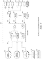
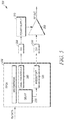
- FIG. 1 shows an exemplary cable television (CATV) system 100 operable to deliver high-definition digital entertainment and telecommunications such as video, voice, and high-speed Internet services.
- CATV cable television
- the CATV system 100 refers to the operational (e.g., geographical) footprint of an entertainment and/or information services franchise that provides entertainment and/or information services to a subscriber base spanning one or more towns, a region, or a portion thereof.
- Particular entertainment and/or information services offered by the franchise e.g., entertainment channel lineup, data packages, etc.
- Some large cable companies operate several cable communication systems (e.g., in some cases up to hundreds of systems), and are known generally as Multiple System Operators (MSOs).
- MSOs Multiple System Operators
- the cable network can take the form of an all-coax, all-fiber, or hybrid fiber/coax (HFC) network, e.g., fiber to the last amplifier (FTTA).
- HFC hybrid fiber/coax
- FIG. 1 depicts a hybrid fiber-coaxial (HFC) network.
- An HFC network is a broadband network that combines optical fiber and coaxial cable, strategically placing fiber nodes to provide services to a plurality of homes. It should be understood that the systems and methods disclosed in the present application may be employed in various networks and the HFC network is merely shown as a non-limiting example.
- the network shown in FIG. 1 is an HFC broadband network that combines the use of optical fiber and coaxial connections.
- the network includes a head end 102 that receives analog video signals and digital bit streams representing different services (e.g., video, voice, and Internet) from various digital information sources.
- the head end 102 may receive content from one or more video on demand (VOD) servers, IPTV broadcast video servers, Internet video sources, or other suitable sources for providing IP content.
- VOD video on demand
- An IP network 108 may include a web server 110 and a data source 112.
- the web server 110 is a streaming server that uses the IP protocol to deliver video-on-demand, audio-on-demand, and pay-per view streams to the IP network 108.
- the IP data source 112 may be connected to a regional area or backbone network (not shown) that transmits IP content.
- the regional area network can be or include the Internet or an IP-based network, a computer network, a web-based network or other suitable wired or wireless network or network system.
- a fiber optic network extends from the cable operator's master/regional head end 102 to a plurality of fiber optic nodes 104.
- the head end 102 may contain an optical transmitter or transceiver to provide optical communications through optical fibers 103.
- Regional head ends and/or neighborhood hub sites may also exist between the head end and one or more nodes.
- the fiber optic portion of the example HFC network 100 extends from the head end 102 to the regional head end/hub and/or to a plurality of nodes 104.
- the optical transmitter converts the electrical signal to a downstream optically modulated signal that is sent to the nodes.
- the optical nodes convert inbound signals to RF energy and return RF signals to optical signals along a return path.
- forward path and downstream may be interchangeably used to refer to a path from a head end to a node, a node to a subscriber, or a head end to a subscriber.
- return path may be interchangeably used to refer to a path from a subscriber to a node, a node to a head end, or a subscriber to a head end.
- a node may be any digital hub between a head end and a customer home that transports local requests over the CATV network.
- Forward path optical communications over the optical fiber may be converted at the nodes to Radio Frequency (RF) communications for transmission over the coaxial cable to the subscribers.
- return path RF communications from the subscribers are provided over coaxial cables and are typically converted at a node to optical signals for transmission over the optical fiber to the head end.
- Each node 104 may contain a return path transmitter that is able to relay communications upstream from a subscriber device 106 to the head end 102.
- Each node 104 serves a service group comprising one or more customer locations.
- a single node 104 may be connected to thousands of cable modems or other subscriber devices 106.
- a fiber node may serve between one and two thousand or more customer locations.
- the fiber optic node 104 may be connected to a plurality of subscriber devices 106 via coaxial cable cascade 111, though those of ordinary skill in the art will appreciate that the coaxial cascade may comprise a combination of RF amplifiers, taps & splitters and coaxial cable.
- each node 104 may include a broadband optical receiver to convert the downstream optically modulated signal received from the head end or a hub to an electrical signal provided to the subscribers' devices 106 through the coaxial cascade 111.
- Signals may pass from the node 104 to the subscriber devices 106 via the RF cascade 111, which may be comprised of multiple amplifiers and active or passive devices including cabling, taps, splitters, and in-line equalizers.
- the amplifiers in the RF cascade 111 may be bidirectional, and may be cascaded such that an amplifier may not only feed an amplifier further along in the cascade but may also feed a large number of subscribers.
- the tap is the customer's drop interface to the coaxial system. Taps are designed in various values to allow amplitude consistency along the distribution system.
- the subscriber devices 106 may reside at a customer location, such as a home of a cable subscriber, and are connected to the cable modem termination system (CMTS) 120 or comparable component located in a head end.
- CMTS cable modem termination system
- a client device 106 may be a modem, e.g., cable modem, MTA (media terminal adaptor), set top box, terminal device, television equipped with set top box, Data Over Cable Service Interface Specification (DOCSIS) terminal device, customer premises equipment (CPE), router, or similar electronic client, end, or terminal devices of subscribers.
- MTA media terminal adaptor
- DOCSIS Data Over Cable Service Interface Specification
- CPE customer premises equipment
- cable modems and IP set top boxes may support data connection to the Internet and other computer networks via the cable network, and the cable network provides bi-directional communication systems in which data can be sent downstream from the head end to a subscriber and upstream from a subscriber to the head end.
- DOCSIS Data Over Cable System Interface Specification
- DOCIS defines the interface requirements for cable modems involved in high-speed data distribution over cable television system networks.
- the techniques disclosed herein may apply to any system for digital services transmission, such as digital video or Ethernet PON over Coax
- CMTS Cable Modem Termination System
- the CMTS is a component located at the head end or hub site of the network that exchanges signals between the head end and client devices within the cable network infrastructure.
- CMTS and the cable modem may be the endpoints of the DOCSIS protocol, with the hybrid fiber coax (HFC) cable plant transmitting information between these endpoints.
- HFC hybrid fiber coax
- architecture 100 includes one CMTS for illustrative purposes only, as it is in fact customary that multiple CMTSs and their Cable Modems are managed through the management network.
- the CMTS 120 hosts downstream and upstream ports and contains numerous receivers, each receiver handling communications between hundreds of end user network elements connected to the broadband network.
- each CMTS 120 may be connected to several modems of many subscribers, e.g., a single CMTS may be connected to hundreds of modems that vary widely in communication characteristics.
- several nodes such as fiber optic nodes 104, may serve a particular area of a town or city.
- DOCSIS enables IP packets to pass between devices on either side of the link between the CMTS and the cable modem.
- CMTS is a non-limiting example of a component in the cable network that may be used to exchange signals between the head end and subscriber devices 106 within the cable network infrastructure.
- M-CMTSTM Modular CMTS
- CCAP Converged Cable Access Platform
- An EdgeQAM (EQAM) 122 or EQAM modulator may be in the head end or hub device for receiving packets of digital content, such as video or data, re-packetizing the digital content into an MPEG transport stream, and digitally modulating the digital transport stream onto a downstream RF carrier using Quadrature Amplitude Modulation (QAM).
- EdgeQAMs may be used for both digital broadcast, and DOCSIS downstream transmission.
- CMTS or M-CMTS implementations data and video QAMs may be implemented on separately managed and controlled platforms.
- the CMTS and edge QAM functionality may be combined in one hardware solution, thereby combining data and video delivery.
- Orthogonal frequency-division multiplexing may utilize smaller subbands (compared to QAM carriers). For example, while a conventional DOCSIS QAM carrier is 6 MHz wide, the CATV system may employ orthogonal frequency division multiplexing (OFDM) technology with OFDM carriers that are approximately 25 kHz to 50 kHz wide. Thus, where previously 100 QAM carriers were used, thousands of OFDM subcarriers may be used. OFDM technology may be suitable for noisy signal conditions and may enable use of more of the available spectrum without reducing the quality of server. In example implementations, a cable network may use the QAM modulation for downstream speeds and boost upstream speeds using OFDM.
- OFDM orthogonal frequency division multiplexing
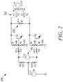
- FIG. 2 shows a representative schematic of a basic push-pull transistor amplifier 200 that amplifies an input signal 210 driven by a differential voltage from supply V2 to produce an output signal 220 through resistor R14.
- the amplifier 100 draws current supplied to two transistors Q1 and Q2 to provide the desired amplified signal voltage across the resistor R12. Resistors R11 and R12 set an input impedance to the amplifier of around 200 Ohms.
- Power supply V4 provides a common voltage to the inputs that is used to set a current bias point of the amplifier.
- Each transistor has a feedback resistor R2 and R4, respectively to the collectors of the transistors, which are connected to the low impedance differential load R10 that is provided the output voltage signal 220 across it.
- Transformer 230 connected to voltage source V1 is also used to bias the amplifier by providing a high impedance to differential signals and a low impedance to common mode current.
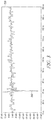
- FIG. 3 shows the input current 250 through resistor R11 and the output current 260 through the resistor R14 of the amplifier circuit 200, for a multi-channel modulated RF signal typical for CATV nodes.
- the current gain is large (> 20x).
- the output amplitude is usually close to an average rms value but occasionally high amplified signal peaks occur.
- the peak values are typically on the order of 6 times the rms value with a relatively low probability (in time) on the order of 10 ⁇ -6.
- the amplifiers must amplify these peaks with high fidelity even though the occurrence rate is relatively low.
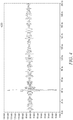
- FIG. 4 shows the amplifier current used by the transistor Q2 in the amplifier 200 of FIG. 2 where the amplifier is biased at approximately 80 mA.
- the current in the transistor Q2 falls to just under 10 mA. At 0 mA the amplifier would have been unable to further amplify the signal and clipping distortion would have occurred.
- RF amplifiers in an HFC network typically operate in a "Class A" mode of operation, meaning that they provide a high fidelity amplified signal where the bit error rate should be no more than approximately 10-8.
- the RF amplifiers in an HFC network must provide a sufficiently high bias point that only approximately one in a hundred or less of the amplified signal peaks are clipped. Because the signal peaks occur so infrequently, however, and because the signal peaks are approximately six times higher than the rms value of the signal, biasing the amplifier to account for the signal peaks makes the amplifier circuit highly inefficient.
- FIG. 5 shows an exemplary receiver 300 capable of being used in a node 104 to modulate an amplifier power supply so as to efficiently attain amplified RF output power with much lower power dissipation than existing amplifiers.
- the receiver 300 may preferably include a decompression module 310 that receives radio frequency data and decompresses it, but could also include other means to generate a digital waveform. Prior to amplifying the decompressed data, the receiver 300 introduces a delay 320 before processing the signal by an optional pre-distortion module 330 and inputting the signal to a D2A converter 340 that drives the input signal to an amplifier 350 having a gain block 360 and power supply 370.
- the receiver 300 preferably includes an analysis module 380 that analyzes the decompressed radio frequency data, i.e. the same data that comprises the input signal to the amplifier 350, and uses the data to create a modulation signal to the power supply 370 through D2A converter 390.
- the modulation signal can comprise any one of a number of alternate forms.
- the power supply 370 may be modulated in a binary manner between a normal (low) bias point used during the periods when the signal is not experiencing signal peaks and a peak (high) bias point when the signal is experiencing signal peaks.
- the bias point of the amplifier 350 may be modulated in a synchronous manner with the signal that it amplifies so that the bias point is raised as the signal experiences a peak and is lowered as the signal falls from the peak.
- more complicated modulation schemes may be employed, such as switching the bias between more than two bias points to account for variances in the amplitudes among signal peaks, or even modulating the bias voltage or current of the amplifier in a manner that is linear with respect to the signal amplitude at any point in time.
- the delay 320 may be introduced at any time before amplifying the data so that the amplified data coincides with the modulation signal, and that the illustration of the delay occurring after decompression is illustrative only, particularly given that some systems may not include compressed data, or otherwise need to decompress data for amplification.
- the receiver 300 may also optionally include many of the components that make up a digital return transmitter, with the addition of an A2D converter.
- the digital forward receiver can thereby perform the function of a digital return transmitter with bandwidths of 85, 2x85, 200 or 2x200 MHz using a bidirectional optical pluggable in the 4.25 Gbs or 11.3 Gbs port.
- the digital forward receiver can be converted to essentially most of the components of a node with forward and reverse traffic for a small added cost.
- the receiver 300 can use signal processing to predict power envelopes and automatically compensate amplifier artifacts due to supply modulation by generating a compensation signal in the output D2A converter.
- the bias point of the amplifier may be modulated to reduce amplifier dissipation.
- the receiver 300 can dissipate on the order of 4 times less supply power for a given output power level. Less power used by the receiver 300 enables the use of smaller transistors, a smaller heat-sink, lower cost packaging, and a reduction of the node size and power consumption.
- embodiments disclosed herein describe a node amplifier solution for power reduction
- the concepts apply for other amplifiers in the cable network.
- embodiments may incorporate modulation of analog amplifiers cascaded in the field that may not be driven directly by D/A converters.
- lower cost amplifiers are desirable.
- embodiments for the cascaded amplifier may provide a lower cost amplifier via the reduction of the power dissipation with a higher output power capability as an option.
- lower cost amplifiers that reduce power dissipation but allow higher output are desirable.
- Embodiments disclosed for creating a more efficient amplifier are beneficial for existing networks and advanced or next generation networks. For example, even if an advanced architecture, e.g., the Node+0 architecture is not adopted, amplifiers that are more power efficient are still desirable. Given that amplifiers compensate for the losses in the leg preceding them, a universal setting from the node works on a collection of amplifiers. As most amplifiers have a similar tilt and gain setting and are operated with a similar power load, by and large the same setting will apply to a chain of amplifiers. Architectures will have shorter and shorter amplifier chains to settle on advanced architectures, e.g., N+1 or N+2.
- the disclosed digital forward architecture permits very low cost and power efficient nodes.
- embodiments for the disclosed digital forward techniques allow small cost and power efficient node designs that enable node replacement and also fiber deep architectures that are currently inhibited by node cost and by maximum wavelength counts on fiber.
- the push and pull transistors may be independently driven by D2A converters to permit true class B operation or class B operation combined with supply modulation. Such manipulations can cause distortions in analog the output signal; however the distortions are predictable.
- the digital pre-distorter 330 in the receiver 300 may optionally be used to mitigate the distortions.
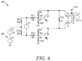
- FIG. 6 depicts an exemplary push-pull amplifier 400 having a power supply 410 capable of being modulated using the receiver 300 such that the bias current is high only when a high peak needs to be amplified and low otherwise by adding a voltage source V3.
- the voltage source V3 is driven by a signal that is generated such that the bias is high when output peaks need to be amplified.
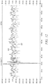
- FIG. 7 shows a waveform 420 representing the voltage provided from the voltage source V3 and a waveform 430 representing the shape of the signal to amplify. The bias signal is seen to increase when an output peak needs to be amplified.
- the bias signal was digitally generated by passing samples of the signal to amplify through a peak detection circuit and a subsequent filter, while the main signal (shown in red in FIG. 7 ) was delayed by a number of samples such that the response of the bias signal would coincide with the signal peak.
- FIG. 8 illustrates an embodiment in which an analysis module 450 may detect both positive and negative peaks, and may calculate the absolute value of the RF signal to amplify before performing a peak detection or power detection operation.
- the amount of delay 460 is set such that the bias signal, after filtering by filter 470, can reach a peak value concurrently with a peak in the RF input signal to amplify.
- the RF signal can be output to a D2A converter to create an analog signal.
- the control bias signal can also be output to a D2A converter to create an analog bias signal.
- FIG. 9 shows that the receiver's amplification of the input signal is unchanged. However, as can be seen in FIG. 10 , the current from the power source V1 is no longer a constant current. The modulation of the bias point of the transistors results in a modulation of the power supply current from the transformer 415 of FIG. 6 .
- FIG. 10 illustrates that when the output signal peak occurs the bias is actually high, peaking as high as 200 mA in this example. On average the bias current is much lower than in the previous example; 82 mA in this case.
- the power consumption of the amplifier has been reduced by a factor of approximately two (as seen in comparison to waveform 430 of FIG. 7 ).
- the transistor currents are shown in FIG. 11 ; as with the comparison for FIG. 11 and FIG. 7 , the comparison of FIG. 11 to FIG. also shows an approximate reduction in power by a factor of two, where the lowest value is again just under 10 mA, but this is accomplished by a bias current of only approximately 40mA per transistor instead of the original 80 mA.
- FIG. 12 illustrates an input signal 500 and output signal 510 that are scaled to approximately the same magnitude and compared; the input signal is amplified and reproduced with high fidelity.
- FIG. 13 shows an analysis module 550 that includes a linearizer 560 that applies a linearization function in the delayed signal path to drive the amplifier, where the parameters of the linearizer can, according to the invention, be controlled by the bias point of the amplifier.
- the implementation of the linearizer can be similar to linearizers used in laser optic transmitters (e.g., linearizer implementations that include digital signal implementations in FPGAs and discrete component implementations in RF components) such as U.S. Patent Nos. 8,064,777 , 8,547,174 and 8,145,066 as well as U.S. Patent Application Pub.
- FIG. 13 is suitable for systems where the signal is digitally processed such that all operations are in the digital domain.
- an implementation in the analog domain with RF components is also possible, including peak detection, delay, bias signal generation and/or linearization functionalities.
- FIG. 14 depicts a push-pull amplifier 600 having two voltage sources 610 and 620 driving the differential transistor amplifier, each voltage source providing both bias control and RF signal information to the transistors.
- the overall signal amplified by the transistors can be the same as in the example depicted in FIGs. 9-11 .
- the amplifier bias current can be controlled and modulated to reduce power dissipation
- the amplifier bias voltage can also be controlled and modulated to reduce power dissipation or a combination thereof.
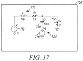
- FIGS. 15-17 show embodiments for a power supply with energy stored in an inductor that supports power delivery during normal operation and during voltage transients
- FIG. 15 shows a power supply 700 with the main power supply 710 set to 11V, for example.
- the power supply 700 may provide current through inductor 715 with a parasitic internal resistance R1 (e.g., a 10 mOhm to 10hm resistor, 900 mOhm in this example).
- a variable voltage source 720 comprising a series connection of first fixed voltage source 725 and a second variable voltage source 730 is shown connected in parallel with the load 735.
- the variable voltage of the voltage supply 730 is made to be proportional to a bias control signal.
- the voltage across load R2 peaks from around 10V to around 22 V, as seen in curve 740.
- the current from power supply 710 seen as curve 745, is fixed at about -1A.
- the current from power supply 720 seen in curve 750 peaks to about -1.2A during the transient, but otherwise it is small (-0.1 A or less). Except for the transient, nearly all the power is delivered by power source 710.
- Power source 720 has enough headroom to provide twice the supply voltage but only delivers power during the transient and while it is delivering power the power source 710 continues to deliver power due to the inductance of the inductor 715 that holds the current constant during the transient.
- the average power delivered by power source 710 (1A) is much larger than the average current from source 720 (0.12 A). Since power source 725 needs to be able to reach 22V it is generally implemented with a 22 V source and a transistor stage following that to create the transient waveform. Thus we can estimate power dissipation in the voltage source 710 can be estimated at 11W (11V x 1A) and the power dissipation in voltage source 720 estimated at 2.64W (22V x 0.12A). The total, 13.64W is much lower than the 25.64W (22V x 1.12A) that would be the case if a fixed 22V power supply was used for the full current.
- some embodiments may replace the voltage supply 725 by a capacitor 760.
- the capacitor 760 may self-charge to around 10V so that an external 22V supply is no longer needed.
- the capacitor 760 is large enough to retain the 10V difference during the surge and the voltage supply 720 can be driven from a 12 V supply; no other higher voltage supply is needed.
- the presence of inductor 715 is essential to keep the current through the transient voltage generator 730 low as the inductor 715 supports the average current during normal operation where the output voltage is close to the main power supply, the main power supply provides all the power, and the inductor 715 sustains that current during transients where the voltage could be much higher (for instance doubled) so that the transient voltage generator only needs to generate the additional current needed excluding the average current that was already provided by L1. Enhanced amplifier operation.
- Computer-readable media may include computer-readable storage media, which corresponds to a tangible medium such as data storage media, or communication media including any medium that facilitates transfer of a computer program from one place to another, e.g., according to a communication protocol.
- Computer-readable media generally may correspond to (1) tangible computer-readable storage media which is non-transitory or (2) a communication medium such as a signal or carrier wave.
- Data storage media may be any available media that can be accessed by one or more computers or one or more processors to retrieve instructions, code and/or data structures for implementation of the techniques described in this disclosure.
- a computer program product may include a computer-readable medium.
- such computer-readable storage media can comprise RAM, ROM, EEPROM, CD-ROM or other optical disk storage, magnetic disk storage, or other magnetic storage devices, flash memory, or any other medium that can be used to store desired program code in the form of instructions or data structures and that can be accessed by a computer.
- any connection is properly termed a computer-readable medium.
- a computer-readable medium For example, if instructions are transmitted from a website, server, or other remote source using a coaxial cable, fiber optic cable, twisted pair, digital subscriber line (DSL), or wireless technologies such as infrared, radio, and microwave, then the coaxial cable, fiber optic cable, twisted pair, DSL, or wireless technologies such as infrared, radio, and microwave are included in the definition of medium.
- DSL digital subscriber line
- disks and data storage media do not include connections, carrier waves, signals, or other transitory media, but are instead directed to non-transitory, tangible storage media.
- processors such as one or more digital signal processors (DSPs), general purpose microprocessors, application specific integrated circuits (ASICs), field programmable logic arrays (FPGAs), or other equivalent integrated or discrete logic circuitry.
- DSPs digital signal processors
- ASICs application specific integrated circuits
- FPGAs field programmable logic arrays
- processors may refer to any of the foregoing structure or any other structure suitable for implementation of the techniques described herein.
- the functionality described herein may be provided within dedicated hardware and/or software modules configured for encoding and decoding, or incorporated in a combined codec. Also, the techniques could be fully implemented in one or more circuits or logic elements.
Landscapes
- Engineering & Computer Science (AREA)
- Power Engineering (AREA)
- Signal Processing (AREA)
- Physics & Mathematics (AREA)
- Computer Networks & Wireless Communication (AREA)
- Multimedia (AREA)
- Electromagnetism (AREA)
- General Physics & Mathematics (AREA)
- Nonlinear Science (AREA)
- Automation & Control Theory (AREA)
- Radar, Positioning & Navigation (AREA)
- Optics & Photonics (AREA)
- General Engineering & Computer Science (AREA)
- Software Systems (AREA)
- Amplifiers (AREA)
- Two-Way Televisions, Distribution Of Moving Picture Or The Like (AREA)
Description
- The present disclosure claims priority to
U.S. Provisional App. No. 61/867,550 - A cable television (CATV) system is capable of providing a variety of media content, such as video, data, voice, or high-speed Internet services to subscribers. The CATV provider typically delivers the media content from a head end to its subscriber's client devices over a transmission network such as a coaxial network, a fiber optic network, or a hybrid fiber/coax (HFC) network. Requirements for data throughput (or bandwidth) in these CATV networks are growing exponentially as customers demand more content, data services, etc. Though improvements in encoding efficiencies and transport protocols have thus far allowed cable operators to keep pace with subscriber and competitive demands, it is important to continue the analysis of the various network elements that can enhance or inhibit the overall performance of next-generation cable networks.
- Most of the radio frequency (RF) amplifiers within the cable television network operate in what is referred to as a "class A" mode of operation, which provides a very high fidelity signal, often quantified in terms of signal-to-noise and signal-to-2nd, 3rd, 4th, 5th... harmonic distortion products. However, the power consumption for the class A mode of operation is on the order of 100 times higher than the composite power of an RF output signal. This higher power consumption results from the need to accommodate significant and frequent 'peak to average' deviations from the effective signal power, which may include setting the output RF rms amplitude of the amplifier at no more than roughly 25% of the output rail-to-rail range of either voltage or current, depending on the implementation. The higher demand for power consumption drives up the cost of cable network products that require RF gain blocs (e.g., head end optical transmitters and receivers, fiber-optic nodes, RF distribution amplifiers). Thus, it is desirable to reduce the power dissipation in a CATV network without compromising output signal power in relation to noise. It would be even more desirable to reduce the power dissipation in a CATV network while improving output signal power in relation to noise.
US-A1-2007/178860 discloses a circuit comprising a delay module that receives a digital transmit signal and that generates a delayed transmit signal. A first digital to analogue converter converts the delayed transmit signal to an analogue transmit signal. An analogue output circuit amplifies the analogue transmit signal. An envelope generating module generates an envelope signal based on amplitude information related to the digital transmit signal. A supply adjustment module supplies a voltage supply reference when the envelope signal is less than a threshold and boosts the bias voltage of the amplifier above the voltage supply reference when the envelope signal is greater than the threshold. - For the purpose of illustrating embodiments described below, there are shown in the drawings example constructions of the embodiments; however, the embodiments are not limited to the specific methods and instrumentalities disclosed. In the drawings:
-
FIG. 1 illustrates an example CATV system. -
FIG. 2 illustrates a schematic diagram of a representative basic push-pull transistor amplifier. -
FIG. 3 illustrates the output current that results from an exemplary input current to the amplifier shown inFIG. 2 -
FIG. 4 illustrates the transistor current provided by the amplifier forFIG. 2 in a biased state when providing the amplified signal ofFIG. 3 . -
FIG. 5 illustrates an embodiment of the disclosed digital forward receiver. -
FIG. 6 illustrates an embodiment for modifying an amplifier biasing. -
FIG. 7 illustrates the shape of a signal to amplify. -
FIG. 8 illustrates an embodiment of a peak detect algorithm. -
FIG. 9 illustrates the input and output waveforms that result from the embodiment shown inFIG. 8 . -
FIG. 10 illustrates an output signal peak when a bias current is high. -
FIG. 11 illustrates exemplary transistor currents. -
FIG. 12 illustrates an input signal and output signal scaled to approximately the same magnitude and compared. -
FIG. 13 illustrates an exemplary linearization function. -
FIG. 14 illustrates an embodiment with two voltage sources driving a transistor amplifier. -
FIG. 15 illustrates a power supply having energy stored in an inductor that supports power delivery during normal operation and during voltage transients. -
FIG. 16 illustrates an exemplary power supply that delivers a fixed current. -
FIG. 17 illustrates an exemplary embodiment that replaces a power supply with a capacitor. - It should be understood that, while the accompanying figures illustrate embodiments that include the portions of the disclosure claimed, and explain various principles and advantages of those embodiments, the details displayed are not necessary to understand the illustrated embodiments, as the details depicted in the figures would be readily apparent to those of ordinary skill in the art having the benefit of the present disclosure.
- The invention is a device for amplifying a Radio Frequency signal according to
claim 1, a method for modulating a bias point of an amplifier according to claim 7, and a system within a CATV network according toclaim 12. - The present disclosure describes systems and methods that reduce power consumption in a CATV network, including (1) systems that improve the power efficiency of a node in a CATV network by drawing power based on a signal; and (2) methods that use signal envelope information to reduce power consumption in a CATV transmission system. As described in more detail later in this specification, disclosed systems and methods utilize and expand on many digital forward path concepts, including but not limited to: 1) analog to digital (A2D) RF signal conversion at one end of a communication link (e.g., at the head end transmitter side for digital forward path transmission); 2) oversampling, i.e. sampling at a rate larger than the Nyquist frequency of twice the sampled bandwidth so as to enable implementation of sharp digital filtering, which reduces the number of binary data bits required for RF signal reassembly; 3) compression coding, e.g., Huffman-type encoding, to further reduce the number of binary bits required for RF signal reassembly; 4) optical on/off transmission over required distances, but less than 100 miles which is limit specified by the Data Over Cable Service Interface Specification (DOCSIS®) standard; and 5) data decompression at a receiver followed by digital to analog (D2A) signal conversion in order to reassemble an originally encoded RF signal from a transmitter.
- Also, the present disclosure describes systems and methods that introduce a delay to be implemented after received data from a signal is decompressed but prior to the decompressed signal data being amplified by a gain block. During the delay, the decompressed data is used to predict the magnitude of the signal envelope that is going to be amplified by the gain block at an incrementally later time. The magnitude of the signal envelope is then used to generate an auxiliary signal that drives the power supply to the RF gain block in a manner that minimizes the required voltage/current for the gain block, and thus minimizes the power consumed by the block. Moreover, a delayed auxiliary signal based on the predicted magnitude of the signal envelope in combination with the, optionally delayed, signal itself can be used as a feed-forward pre-distortion signal that corrects for distortion introduced by the RF gain block when amplifying the signal envelope.
- The systems and methods disclosed in the present application can be particularly useful for reducing the power consumption of a fiber optical node that has a large number of RF outputs, and acts as the last amplifier before servicing customer premises - in architectures alternatively referred to as "fiber to the last active" (FTTLA), Node plus zero (N+0), or fiber deep architectures - because in such nodes the RF signals at the output of the node typically consume a relatively large amount of power. It should be understood, however, that other architectures or components of other architectures may benefit from the disclosed techniques, such as upstream or return path A2D/D2A systems, or digital return receivers. Further, the disclosed techniques could be applied to regulating RF gain stages of other digital forward receivers, even if the receiver is not the last RF gain stage in the downstream architecture. Additional details for various embodiments are described in more detail below.
-
FIG. 1 shows an exemplary cable television (CATV)system 100 operable to deliver high-definition digital entertainment and telecommunications such as video, voice, and high-speed Internet services. Generally speaking, theCATV system 100 refers to the operational (e.g., geographical) footprint of an entertainment and/or information services franchise that provides entertainment and/or information services to a subscriber base spanning one or more towns, a region, or a portion thereof. Particular entertainment and/or information services offered by the franchise (e.g., entertainment channel lineup, data packages, etc.) may differ from system to system. Some large cable companies operate several cable communication systems (e.g., in some cases up to hundreds of systems), and are known generally as Multiple System Operators (MSOs). - The cable network can take the form of an all-coax, all-fiber, or hybrid fiber/coax (HFC) network, e.g., fiber to the last amplifier (FTTA). For purposes of illustration only,
FIG. 1 depicts a hybrid fiber-coaxial (HFC) network. An HFC network is a broadband network that combines optical fiber and coaxial cable, strategically placing fiber nodes to provide services to a plurality of homes. It should be understood that the systems and methods disclosed in the present application may be employed in various networks and the HFC network is merely shown as a non-limiting example. - The network shown in
FIG. 1 is an HFC broadband network that combines the use of optical fiber and coaxial connections. The network includes ahead end 102 that receives analog video signals and digital bit streams representing different services (e.g., video, voice, and Internet) from various digital information sources. For example, thehead end 102 may receive content from one or more video on demand (VOD) servers, IPTV broadcast video servers, Internet video sources, or other suitable sources for providing IP content. - An
IP network 108 may include aweb server 110 and a data source 112. Theweb server 110 is a streaming server that uses the IP protocol to deliver video-on-demand, audio-on-demand, and pay-per view streams to theIP network 108. The IP data source 112 may be connected to a regional area or backbone network (not shown) that transmits IP content. For example, the regional area network can be or include the Internet or an IP-based network, a computer network, a web-based network or other suitable wired or wireless network or network system. - At the
head end 102, the various services are encoded, modulated and up-converted onto RF carriers, combined onto a single electrical signal and inserted into a broadband optical transmitter. A fiber optic network extends from the cable operator's master/regional head end 102 to a plurality offiber optic nodes 104. Thehead end 102 may contain an optical transmitter or transceiver to provide optical communications throughoptical fibers 103. Regional head ends and/or neighborhood hub sites may also exist between the head end and one or more nodes. The fiber optic portion of theexample HFC network 100 extends from thehead end 102 to the regional head end/hub and/or to a plurality ofnodes 104. The optical transmitter converts the electrical signal to a downstream optically modulated signal that is sent to the nodes. In turn, the optical nodes convert inbound signals to RF energy and return RF signals to optical signals along a return path. In the specification, the drawings, and the claims, the terms "forward path" and "downstream" may be interchangeably used to refer to a path from a head end to a node, a node to a subscriber, or a head end to a subscriber. Conversely, the terms "return path", "reverse path" and "upstream" may be interchangeably used to refer to a path from a subscriber to a node, a node to a head end, or a subscriber to a head end. Also, in the specification, in the drawings, and the claims a node may be any digital hub between a head end and a customer home that transports local requests over the CATV network. Forward path optical communications over the optical fiber may be converted at the nodes to Radio Frequency (RF) communications for transmission over the coaxial cable to the subscribers. Conversely, return path RF communications from the subscribers are provided over coaxial cables and are typically converted at a node to optical signals for transmission over the optical fiber to the head end. Eachnode 104 may contain a return path transmitter that is able to relay communications upstream from asubscriber device 106 to thehead end 102. - Each
node 104 serves a service group comprising one or more customer locations. By way of example, asingle node 104 may be connected to thousands of cable modems orother subscriber devices 106. In an example, a fiber node may serve between one and two thousand or more customer locations. In an HFC network, thefiber optic node 104 may be connected to a plurality ofsubscriber devices 106 via coaxial cable cascade 111, though those of ordinary skill in the art will appreciate that the coaxial cascade may comprise a combination of RF amplifiers, taps & splitters and coaxial cable. In some implementations, eachnode 104 may include a broadband optical receiver to convert the downstream optically modulated signal received from the head end or a hub to an electrical signal provided to the subscribers'devices 106 through the coaxial cascade 111. Signals may pass from thenode 104 to thesubscriber devices 106 via the RF cascade 111, which may be comprised of multiple amplifiers and active or passive devices including cabling, taps, splitters, and in-line equalizers. It should be understood that the amplifiers in the RF cascade 111 may be bidirectional, and may be cascaded such that an amplifier may not only feed an amplifier further along in the cascade but may also feed a large number of subscribers. The tap is the customer's drop interface to the coaxial system. Taps are designed in various values to allow amplitude consistency along the distribution system. - The
subscriber devices 106 may reside at a customer location, such as a home of a cable subscriber, and are connected to the cable modem termination system (CMTS) 120 or comparable component located in a head end. Aclient device 106 may be a modem, e.g., cable modem, MTA (media terminal adaptor), set top box, terminal device, television equipped with set top box, Data Over Cable Service Interface Specification (DOCSIS) terminal device, customer premises equipment (CPE), router, or similar electronic client, end, or terminal devices of subscribers. For example, cable modems and IP set top boxes may support data connection to the Internet and other computer networks via the cable network, and the cable network provides bi-directional communication systems in which data can be sent downstream from the head end to a subscriber and upstream from a subscriber to the head end. - The techniques disclosed herein may be applied to systems compliant with DOCSIS. The cable industry developed the international Data Over Cable System Interface Specification (DOCSIS®) standard or protocol to enable the delivery of IP data packets over cable systems. In general, DOCSIS defines the communications and operations support interface requirements for a data over cable system. For example, DOCIS defines the interface requirements for cable modems involved in high-speed data distribution over cable television system networks. However, it should be understood that the techniques disclosed herein may apply to any system for digital services transmission, such as digital video or Ethernet PON over Coax
- (EPoc). Examples herein referring to DOCSIS are illustrative and representative of the application of the techniques to a broad range of services carried over coax.
- References are made in the present disclosure to a Cable Modem Termination System (CMTS) in the
head end 102. In general, the CMTS is a component located at the head end or hub site of the network that exchanges signals between the head end and client devices within the cable network infrastructure. In an example DOCSIS arrangement, for example, the CMTS and the cable modem may be the endpoints of the DOCSIS protocol, with the hybrid fiber coax (HFC) cable plant transmitting information between these endpoints. It will be appreciated thatarchitecture 100 includes one CMTS for illustrative purposes only, as it is in fact customary that multiple CMTSs and their Cable Modems are managed through the management network. - The
CMTS 120 hosts downstream and upstream ports and contains numerous receivers, each receiver handling communications between hundreds of end user network elements connected to the broadband network. For example, eachCMTS 120 may be connected to several modems of many subscribers, e.g., a single CMTS may be connected to hundreds of modems that vary widely in communication characteristics. In many instances several nodes, such asfiber optic nodes 104, may serve a particular area of a town or city. DOCSIS enables IP packets to pass between devices on either side of the link between the CMTS and the cable modem. - It should be understood that the CMTS is a non-limiting example of a component in the cable network that may be used to exchange signals between the head end and
subscriber devices 106 within the cable network infrastructure. For example, other non-limiting examples include a Modular CMTS (M-CMTSTM) architecture or a Converged Cable Access Platform (CCAP). - An EdgeQAM (EQAM) 122 or EQAM modulator may be in the head end or hub device for receiving packets of digital content, such as video or data, re-packetizing the digital content into an MPEG transport stream, and digitally modulating the digital transport stream onto a downstream RF carrier using Quadrature Amplitude Modulation (QAM). EdgeQAMs may be used for both digital broadcast, and DOCSIS downstream transmission. In CMTS or M-CMTS implementations, data and video QAMs may be implemented on separately managed and controlled platforms. In CCAP implementations, the CMTS and edge QAM functionality may be combined in one hardware solution, thereby combining data and video delivery.
- Orthogonal frequency-division multiplexing (OFDM) may utilize smaller subbands (compared to QAM carriers). For example, while a conventional DOCSIS QAM carrier is 6 MHz wide, the CATV system may employ orthogonal frequency division multiplexing (OFDM) technology with OFDM carriers that are approximately 25 kHz to 50 kHz wide. Thus, where previously 100 QAM carriers were used, thousands of OFDM subcarriers may be used. OFDM technology may be suitable for noisy signal conditions and may enable use of more of the available spectrum without reducing the quality of server. In example implementations, a cable network may use the QAM modulation for downstream speeds and boost upstream speeds using OFDM.
-
FIG. 2 shows a representative schematic of a basic push-pull transistor amplifier 200 that amplifies aninput signal 210 driven by a differential voltage from supply V2 to produce anoutput signal 220 through resistor R14. Theamplifier 100 draws current supplied to two transistors Q1 and Q2 to provide the desired amplified signal voltage across the resistor R12. Resistors R11 and R12 set an input impedance to the amplifier of around 200 Ohms. Power supply V4 provides a common voltage to the inputs that is used to set a current bias point of the amplifier. Each transistor has a feedback resistor R2 and R4, respectively to the collectors of the transistors, which are connected to the low impedance differential load R10 that is provided theoutput voltage signal 220 across it.Transformer 230 connected to voltage source V1 is also used to bias the amplifier by providing a high impedance to differential signals and a low impedance to common mode current. -
FIG. 3 shows the input current 250 through resistor R11 and the output current 260 through the resistor R14 of theamplifier circuit 200, for a multi-channel modulated RF signal typical for CATV nodes. The current gain is large (> 20x). The output amplitude is usually close to an average rms value but occasionally high amplified signal peaks occur. The peak values are typically on the order of 6 times the rms value with a relatively low probability (in time) on the order of 10^-6. However, since amplifier clipping leads to bit errors in RF communication links, the amplifiers must amplify these peaks with high fidelity even though the occurrence rate is relatively low. - In order to provide the required current gain to amplify a signal with the large signal peaks shown in
FIG. 3 , the amplifier must usually be biased at a high current. Thus can be most easily seen inFIG. 4 , which shows the amplifier current used by the transistor Q2 in theamplifier 200 ofFIG. 2 where the amplifier is biased at approximately 80 mA. When amplifying thesignal 250 shown inFIG. 3 , during the peak in output voltage the current in the transistor Q2 falls to just under 10 mA. At 0 mA the amplifier would have been unable to further amplify the signal and clipping distortion would have occurred. Stated differently, were theamplifier circuit 200 not biased to 80 mA but biased at a lower point, or alternatively, if the input to the amplifier had a higher signal peak to be amplified, clipping would have occurred along with the attendant signal degradation (bit error) that accompanies distortion from amplifier clipping. - RF amplifiers in an HFC network typically operate in a "Class A" mode of operation, meaning that they provide a high fidelity amplified signal where the bit error rate should be no more than approximately 10-8. As just noted, given that the signal peaks occur at a rate of 10-6, i.e. 100 times the frequency of the required bit error rate, the RF amplifiers in an HFC network must provide a sufficiently high bias point that only approximately one in a hundred or less of the amplified signal peaks are clipped. Because the signal peaks occur so infrequently, however, and because the signal peaks are approximately six times higher than the rms value of the signal, biasing the amplifier to account for the signal peaks makes the amplifier circuit highly inefficient. In a typical case, for example, to provide 100mW of total RF output of the amplified signal, about 10W of power is required, i.e. only about 1% of the power supply to the amplifier is used to provide the RF energy output while the remainder of the power is consumed to bias the amplifier at a current that is almost always much higher than necessary to amplify the signal, except for the infrequent signal peaks.
- There are more than four million amplifiers dispersed throughout HFC networks in the United States alone. This translates into a total energy consumption in the millions of dollars per year, which as just noted is mostly energy that is only needed to amplify highly sporadic signal peaks.
-
FIG. 5 shows anexemplary receiver 300 capable of being used in anode 104 to modulate an amplifier power supply so as to efficiently attain amplified RF output power with much lower power dissipation than existing amplifiers. Thereceiver 300 may preferably include a decompression module 310 that receives radio frequency data and decompresses it, but could also include other means to generate a digital waveform. Prior to amplifying the decompressed data, thereceiver 300 introduces adelay 320 before processing the signal by anoptional pre-distortion module 330 and inputting the signal to aD2A converter 340 that drives the input signal to anamplifier 350 having again block 360 andpower supply 370. - During the
delay 320, thereceiver 300 preferably includes ananalysis module 380 that analyzes the decompressed radio frequency data, i.e. the same data that comprises the input signal to theamplifier 350, and uses the data to create a modulation signal to thepower supply 370 throughD2A converter 390. The modulation signal can comprise any one of a number of alternate forms. For example, in a simple embodiment, thepower supply 370 may be modulated in a binary manner between a normal (low) bias point used during the periods when the signal is not experiencing signal peaks and a peak (high) bias point when the signal is experiencing signal peaks. Because of thedelay 320, the bias point of theamplifier 350 may be modulated in a synchronous manner with the signal that it amplifies so that the bias point is raised as the signal experiences a peak and is lowered as the signal falls from the peak. In other embodiments, more complicated modulation schemes may be employed, such as switching the bias between more than two bias points to account for variances in the amplitudes among signal peaks, or even modulating the bias voltage or current of the amplifier in a manner that is linear with respect to the signal amplitude at any point in time. It should be understood that thedelay 320 may be introduced at any time before amplifying the data so that the amplified data coincides with the modulation signal, and that the illustration of the delay occurring after decompression is illustrative only, particularly given that some systems may not include compressed data, or otherwise need to decompress data for amplification. - The
receiver 300 may also optionally include many of the components that make up a digital return transmitter, with the addition of an A2D converter. The digital forward receiver can thereby perform the function of a digital return transmitter with bandwidths of 85, 2x85, 200 or 2x200 MHz using a bidirectional optical pluggable in the 4.25 Gbs or 11.3 Gbs port. Thus, the digital forward receiver can be converted to essentially most of the components of a node with forward and reverse traffic for a small added cost. - As can be appreciated by those of ordinary skill in the art, the
receiver 300 can use signal processing to predict power envelopes and automatically compensate amplifier artifacts due to supply modulation by generating a compensation signal in the output D2A converter. The bias point of the amplifier (current and/or voltage) may be modulated to reduce amplifier dissipation. In some embodiments, thereceiver 300 can dissipate on the order of 4 times less supply power for a given output power level. Less power used by thereceiver 300 enables the use of smaller transistors, a smaller heat-sink, lower cost packaging, and a reduction of the node size and power consumption. - It should be noted that while embodiments disclosed herein describe a node amplifier solution for power reduction, the concepts apply for other amplifiers in the cable network. For example, embodiments may incorporate modulation of analog amplifiers cascaded in the field that may not be driven directly by D/A converters. In an amplifier in the cascade of amplifiers, lower cost amplifiers are desirable. As disclosed, embodiments for the cascaded amplifier may provide a lower cost amplifier via the reduction of the power dissipation with a higher output power capability as an option. Where the cable network has been upgraded, lower cost amplifiers that reduce power dissipation but allow higher output are desirable.
- Embodiments disclosed for creating a more efficient amplifier are beneficial for existing networks and advanced or next generation networks. For example, even if an advanced architecture, e.g., the Node+0 architecture is not adopted, amplifiers that are more power efficient are still desirable. Given that amplifiers compensate for the losses in the leg preceding them, a universal setting from the node works on a collection of amplifiers. As most amplifiers have a similar tilt and gain setting and are operated with a similar power load, by and large the same setting will apply to a chain of amplifiers. Architectures will have shorter and shorter amplifier chains to settle on advanced architectures, e.g., N+1 or N+2.
- The disclosed digital forward architecture permits very low cost and power efficient nodes. For example, embodiments for the disclosed digital forward techniques allow small cost and power efficient node designs that enable node replacement and also fiber deep architectures that are currently inhibited by node cost and by maximum wavelength counts on fiber. Furthermore, in embodiments where all processing is in the digital domain, there is flexibility in the band-split of such a design. Almost any RF gain stage can benefit from the disclosed techniques where a digitized input signal is made, delayed, and used as a decision input for a power supply and predistortion input. Existing standard HFC gain stages do not have a benefit of the digitized signal, thus the disclosed digital forward (and digital return) systems disclosed may benefit from the disclosed techniques for the receiving side of the system and the corresponding output RF gain stage (with a cost effective, minimal functional blocks/cost addition).
- It should be noted that various implementations for the disclosed techniques are possible wherein the supply voltage and/or the transistor bias are modulated. The push and pull transistors may be independently driven by D2A converters to permit true class B operation or class B operation combined with supply modulation. Such manipulations can cause distortions in analog the output signal; however the distortions are predictable. The
digital pre-distorter 330 in thereceiver 300 may optionally be used to mitigate the distortions. -
FIG. 6 depicts an exemplary push-pull amplifier 400 having apower supply 410 capable of being modulated using thereceiver 300 such that the bias current is high only when a high peak needs to be amplified and low otherwise by adding a voltage source V3. The voltage source V3 is driven by a signal that is generated such that the bias is high when output peaks need to be amplified.FIG. 7 shows awaveform 420 representing the voltage provided from the voltage source V3 and awaveform 430 representing the shape of the signal to amplify. The bias signal is seen to increase when an output peak needs to be amplified. In the embodiment depicted inFIGS. 6 and7 , the bias signal was digitally generated by passing samples of the signal to amplify through a peak detection circuit and a subsequent filter, while the main signal (shown in red inFIG. 7 ) was delayed by a number of samples such that the response of the bias signal would coincide with the signal peak. -
FIG. 8 illustrates an embodiment in which ananalysis module 450 may detect both positive and negative peaks, and may calculate the absolute value of the RF signal to amplify before performing a peak detection or power detection operation. The amount ofdelay 460 is set such that the bias signal, after filtering byfilter 470, can reach a peak value concurrently with a peak in the RF input signal to amplify. The RF signal can be output to a D2A converter to create an analog signal. The control bias signal can also be output to a D2A converter to create an analog bias signal. - Resulting
input waveform 480 andoutput waveform 490 from the embodiment ofFIG. 8 are each shown inFIG. 9 , which can be easily seen as a reproduction of the input and output waveforms ofFig, 3 .FIG. 9 shows that the receiver's amplification of the input signal is unchanged. However, as can be seen inFIG. 10 , the current from the power source V1 is no longer a constant current. The modulation of the bias point of the transistors results in a modulation of the power supply current from thetransformer 415 ofFIG. 6 .FIG. 10 illustrates that when the output signal peak occurs the bias is actually high, peaking as high as 200 mA in this example. On average the bias current is much lower than in the previous example; 82 mA in this case. The power consumption of the amplifier has been reduced by a factor of approximately two (as seen in comparison towaveform 430 ofFIG. 7 ). The transistor currents are shown inFIG. 11 ; as with the comparison forFIG. 11 andFIG. 7 , the comparison ofFIG. 11 to FIG. also shows an approximate reduction in power by a factor of two, where the lowest value is again just under 10 mA, but this is accomplished by a bias current of only approximately 40mA per transistor instead of the original 80 mA. - Because the power supply via
transformer 415 ofFIG. 6 is insensitive to common mode current fluctuations (these are passed with little resistance) and because the differential output signal in R14 is also not sensitive to common mode fluctuations, the push-pull amplifier shown inFIG. 6 is particularly suitable for modulation of the bias current without affecting the signal to amplify because the bias control signal is self-cancelled in the output resistor R14.FIG. 12 illustrates aninput signal 500 and output signal 510 that are scaled to approximately the same magnitude and compared; the input signal is amplified and reproduced with high fidelity. - In CATV systems, however, extreme requirements can be applied to the fidelity of signal amplification. It is known that there is some dependence of the distortion behavior of amplifiers on the bias point. Accordingly,
FIG. 13 shows ananalysis module 550 that includes alinearizer 560 that applies a linearization function in the delayed signal path to drive the amplifier, where the parameters of the linearizer can, according to the invention, be controlled by the bias point of the amplifier. The implementation of the linearizer can be similar to linearizers used in laser optic transmitters (e.g., linearizer implementations that include digital signal implementations in FPGAs and discrete component implementations in RF components) such asU.S. Patent Nos. 8,064,777 ,8,547,174 and8,145,066 as well asU.S. Patent Application Pub. No. 20030001670 . The embodiment shown inFIG. 13 is suitable for systems where the signal is digitally processed such that all operations are in the digital domain. However, it should be understood that an implementation in the analog domain with RF components is also possible, including peak detection, delay, bias signal generation and/or linearization functionalities. - It should also be understood that in some embodiments, the bias control signal and the RF signal to amplify need not be generated separately on D2A converters. For example,
FIG. 14 depicts a push-pull amplifier 600 having twovoltage sources FIGs. 9-11 . Moreover, while the amplifier bias current can be controlled and modulated to reduce power dissipation, the amplifier bias voltage can also be controlled and modulated to reduce power dissipation or a combination thereof. - In some embodiments where the power supply is modulated, the combination of bias current and voltage supply modulation can yield further power savings, for instance by a factor of four instead of a factor of two as was shown with bias modulation only. However, the construction of a modulated voltage supply is more complex than modulating the bias current of the transistors.
FIGS. 15-17 show embodiments for a power supply with energy stored in an inductor that supports power delivery during normal operation and during voltage transientsFIG. 15 , for example, shows apower supply 700 with themain power supply 710 set to 11V, for example. Thepower supply 700 may provide current throughinductor 715 with a parasitic internal resistance R1 (e.g., a 10 mOhm to 10hm resistor, 900 mOhm in this example). Avariable voltage source 720 comprising a series connection of first fixedvoltage source 725 and a secondvariable voltage source 730 is shown connected in parallel with theload 735. The variable voltage of thevoltage supply 730 is made to be proportional to a bias control signal. - As shown in
FIG. 16 , in a bias voltage control transient, the voltage across load R2 peaks from around 10V to around 22 V, as seen incurve 740. The current frompower supply 710, seen as curve 745, is fixed at about -1A. The current frompower supply 720, seen incurve 750 peaks to about -1.2A during the transient, but otherwise it is small (-0.1 A or less). Except for the transient, nearly all the power is delivered bypower source 710.Power source 720 has enough headroom to provide twice the supply voltage but only delivers power during the transient and while it is delivering power thepower source 710 continues to deliver power due to the inductance of theinductor 715 that holds the current constant during the transient. As a result the average power delivered by power source 710 (1A) is much larger than the average current from source 720 (0.12 A). Sincepower source 725 needs to be able to reach 22V it is generally implemented with a 22 V source and a transistor stage following that to create the transient waveform. Thus we can estimate power dissipation in thevoltage source 710 can be estimated at 11W (11V x 1A) and the power dissipation involtage source 720 estimated at 2.64W (22V x 0.12A). The total, 13.64W is much lower than the 25.64W (22V x 1.12A) that would be the case if a fixed 22V power supply was used for the full current. - As shown in
FIG. 17 , some embodiments may replace thevoltage supply 725 by acapacitor 760. In this example, thecapacitor 760 may self-charge to around 10V so that an external 22V supply is no longer needed. Thecapacitor 760 is large enough to retain the 10V difference during the surge and thevoltage supply 720 can be driven from a 12 V supply; no other higher voltage supply is needed. - In some embodiments, the presence of
inductor 715 is essential to keep the current through thetransient voltage generator 730 low as theinductor 715 supports the average current during normal operation where the output voltage is close to the main power supply, the main power supply provides all the power, and theinductor 715 sustains that current during transients where the voltage could be much higher (for instance doubled) so that the transient voltage generator only needs to generate the additional current needed excluding the average current that was already provided by L1. Enhanced amplifier operation. - In one or more examples, the functions disclosed herein may be implemented in hardware, software, firmware, or any combination thereof. If implemented in software, the functions may be stored on or transmitted as one or more instructions or code on a computer-readable medium and executed by a hardware-based processing unit. Computer-readable media may include computer-readable storage media, which corresponds to a tangible medium such as data storage media, or communication media including any medium that facilitates transfer of a computer program from one place to another, e.g., according to a communication protocol. In this manner, computer-readable media generally may correspond to (1) tangible computer-readable storage media which is non-transitory or (2) a communication medium such as a signal or carrier wave. Data storage media may be any available media that can be accessed by one or more computers or one or more processors to retrieve instructions, code and/or data structures for implementation of the techniques described in this disclosure. A computer program product may include a computer-readable medium.
- By way of example, and not limitation, such computer-readable storage media can comprise RAM, ROM, EEPROM, CD-ROM or other optical disk storage, magnetic disk storage, or other magnetic storage devices, flash memory, or any other medium that can be used to store desired program code in the form of instructions or data structures and that can be accessed by a computer. Also, any connection is properly termed a computer-readable medium. For example, if instructions are transmitted from a website, server, or other remote source using a coaxial cable, fiber optic cable, twisted pair, digital subscriber line (DSL), or wireless technologies such as infrared, radio, and microwave, then the coaxial cable, fiber optic cable, twisted pair, DSL, or wireless technologies such as infrared, radio, and microwave are included in the definition of medium. It should be understood, however, that computer-readable storage media and data storage media do not include connections, carrier waves, signals, or other transitory media, but are instead directed to non-transitory, tangible storage media. "Disk" and "disc" as used herein, includes compact disc (CD), laser disc, optical disc, digital versatile disc (DVD), floppy disk and Blu-ray disc where disks usually reproduce data magnetically, while discs reproduce data optically with lasers. Combinations of the above should also be included within the scope of computer-readable media.
- Instructions may be executed by one or more processors, such as one or more digital signal processors (DSPs), general purpose microprocessors, application specific integrated circuits (ASICs), field programmable logic arrays (FPGAs), or other equivalent integrated or discrete logic circuitry. Accordingly, the term "processor," as used herein may refer to any of the foregoing structure or any other structure suitable for implementation of the techniques described herein. In addition, in some aspects, the functionality described herein may be provided within dedicated hardware and/or software modules configured for encoding and decoding, or incorporated in a combined codec. Also, the techniques could be fully implemented in one or more circuits or logic elements.
- The techniques of this disclosure may be implemented in a wide variety of devices or apparatuses. Various components, modules, or units are described in this disclosure to emphasize functional aspects of components configured to perform the disclosed techniques, but do not necessarily require realization by different hardware units. Rather, as described above, various units may be combined in a codec hardware unit or provided by a collection of interoperative hardware units, including one or more processors as described above, in conjunction with suitable software and/or firmware.
Claims (15)
- A device for amplifying a Radio Frequency signal, the device comprising:a decompression module (310) arranged to receive radio frequency data and to decompress the received radio frequency data to generate decompressed radio frequency data;a delay module (320) arranged to introduce a delay;an analysis module (380) arranged to analyze the decompressed radio frequency data and to create a modulation signal;amplifier (350) arranged to amplify the decompressed radio frequency data, the amplifier (350) having a power supply (370);wherein the power supply (370) is modulated by the modulation signal such that a bias point of the amplifier (350) is modulated in a synchronous manner with the decompressed radio frequency data so that the bias point is raised as the signal experiences a peak and is lowered as the signal falls from the peak;wherein the analysis module (380) includes a linearizer (560), the linearizer (560) arranged to apply a linearization function in the delayed signal path to drive the amplifier (350), and wherein parameters of the linearizer are controlled by the bias point of the amplifier (350).
- The device of claim 1, further comprising a D2A converter (340) that receives the modulation signal from the analysis module (380) and provides an output signal for modulating the power supply (370).
- The device of claim 1 or 2, wherein the amplifier (350) has a gain block (360).
- The device of any preceding claim, wherein the bias point is switched between more than two bias points to account for variances in the amplitudes among signal peaks.
- The device of any of claims 1 to 3, wherein the bias point of the amplifier is modulated in a manner that is linear with respect to the received radio frequency data.
- The device of any preceding claim, wherein the delay module (320) is arranged between the decompression module (310) and the amplifier (350).
- A method for modulating a bias point of an amplifier (350), the method comprising:receiving radio frequency data;decompressing the received radio frequency data to generate decompressed radio frequency data;introducing a delay (320);analyzing (380) the decompressed radio frequency data and to create a modulation signal;amplifying the decompressed radio frequency data by an amplifier (350), wherein an amplifier power supply (370) is modulated by the modulation signal such that a bias point of the amplifier (350) is modulated in a synchronous manner with the decompressed radio frequency data so that the bias point is raised as the signal experiences a peak and is lowered as the signal falls from the peak;wherein the analysis (380) includes linearization (560), the linearization (560) comprising application of a linearization function in the delayed signal path to drive the amplification step (350), and wherein parameters of the linearization (560) are controlled by the bias point of the amplification.
- The method of claim 7, further comprising a digital to analogue conversion of the modulation signal to provide an output signal for modulating the amplifier power supply (370).
- The method of claim 7 or 8, wherein the bias point is switched between more than two bias points to account for variances in the amplitudes among signal peaks.
- The method of claim 7 or 8, wherein the bias point of the amplifier is modulated in a manner that is linear with respect to the received radio frequency data.
- The method of any of claims 7 to 10, wherein the delay (320) is introduced between the decompression step (310) and the amplification step (350).
- A system within a CATV network for reducing a power usage of an amplifier (350), said system comprising:a decompression module (310) arranged to receive radio frequency data and to decompress the received radio frequency data to generate decompressed radio frequency data;a delay module (320) arranged to introduce a delay;an analysis module (380) arranged to analyze the decompressed radio frequency data and to create a modulation signal;amplifier (350) arranged to amplify the decompressed radio frequency data, the amplifier (350) having a power supply (370);wherein the power supply (370) is modulated by the modulation signal such that a bias point of the amplifier (350) is modulated in a synchronous manner with the decompressed radio frequency data so that the bias point is raised as the signal experiences a peak and is lowered as the signal falls from the peak;wherein the analysis module (380) includes a linearizer (560), the linearizer (560) arranged to apply a linearization function in the delayed signal path to drive the amplifier (350), and wherein parameters of the linearizer are controlled by the bias point of the amplifier (350).
- The device of claim 12, further comprising a D2A converter (340) that receives the modulation signal from the analysis module (380) and provides an output signal for modulating the power supply (370).
- The system of claim 12 or 13, wherein the bias point is switched between more than two bias points to account for variances in the amplitudes among signal peaks.
- The system of claim 12 or 13, wherein the bias point of the amplifier is modulated in a manner that is linear with respect to the received radio frequency data.
Priority Applications (1)
| Application Number | Priority Date | Filing Date | Title |
|---|---|---|---|
| EP20201625.9A EP3826235A1 (en) | 2013-08-19 | 2014-08-19 | Device for modulating an amplifier power supply |
Applications Claiming Priority (2)
| Application Number | Priority Date | Filing Date | Title |
|---|---|---|---|
| US201361867550P | 2013-08-19 | 2013-08-19 | |
| PCT/US2014/051663 WO2015026807A1 (en) | 2013-08-19 | 2014-08-19 | Fiber-optic node with forward data content driven power consumption |
Related Child Applications (1)
| Application Number | Title | Priority Date | Filing Date |
|---|---|---|---|
| EP20201625.9A Division EP3826235A1 (en) | 2013-08-19 | 2014-08-19 | Device for modulating an amplifier power supply |
Publications (2)
| Publication Number | Publication Date |
|---|---|
| EP3036868A1 EP3036868A1 (en) | 2016-06-29 |
| EP3036868B1 true EP3036868B1 (en) | 2020-10-14 |
Family
ID=52466842
Family Applications (2)
| Application Number | Title | Priority Date | Filing Date |
|---|---|---|---|
| EP14762129.6A Active EP3036868B1 (en) | 2013-08-19 | 2014-08-19 | Fiber-optic node with forward data content driven power consumption |
| EP20201625.9A Pending EP3826235A1 (en) | 2013-08-19 | 2014-08-19 | Device for modulating an amplifier power supply |
Family Applications After (1)
| Application Number | Title | Priority Date | Filing Date |
|---|---|---|---|
| EP20201625.9A Pending EP3826235A1 (en) | 2013-08-19 | 2014-08-19 | Device for modulating an amplifier power supply |
Country Status (9)
| Country | Link |
|---|---|
| US (5) | US9191064B2 (en) |
| EP (2) | EP3036868B1 (en) |
| JP (2) | JP6685908B2 (en) |
| KR (1) | KR101817884B1 (en) |
| CA (2) | CA3129289C (en) |
| CL (1) | CL2016000360A1 (en) |
| ES (1) | ES2831798T3 (en) |
| MX (1) | MX349316B (en) |
| WO (1) | WO2015026807A1 (en) |
Families Citing this family (15)
| Publication number | Priority date | Publication date | Assignee | Title |
|---|---|---|---|---|
| US20070093157A1 (en) | 2005-10-20 | 2007-04-26 | Kimberly-Clark Worldwide, Inc. | High speed, pressure bonded, thin sheet laminate |
| WO2015026801A1 (en) | 2013-08-19 | 2015-02-26 | Arris Enterprises, Inc. | R-ccap with am star architecture |
| WO2016187055A1 (en) * | 2015-05-15 | 2016-11-24 | Crocus Technology Inc. | Mram-based pre-distortion linearization and amplification circuits |
| EP3335314A1 (en) * | 2015-08-14 | 2018-06-20 | Viasat, Inc. | Digital dynamic bias circuit |
| CN105933747A (en) * | 2016-06-20 | 2016-09-07 | 深圳市健马科技开发有限公司 | Multichannel network audio/video smart power amplifier and smart power amplifier system |
| US10033330B2 (en) | 2016-12-22 | 2018-07-24 | Arris Enterprises Llc | Amplifier with power dissipation reduction using single radio frequency digital-to-analog converter |
| US10218318B2 (en) | 2017-07-20 | 2019-02-26 | Arris Enterprises Llc | Amplifier with digital linearization and multiple output stages |
| WO2019086748A1 (en) | 2017-11-06 | 2019-05-09 | Teleste Oyj | An arrangement for catv network segmentation |
| CA3080940A1 (en) * | 2017-11-06 | 2019-05-09 | Teleste Oyj | An arrangement for catv network segmentation |
| US10523459B2 (en) | 2017-12-18 | 2019-12-31 | Arris Enterprises Llc | Systems and methods for power savings in HFC amplifiers |
| US11121528B2 (en) | 2018-05-22 | 2021-09-14 | Charter Communications Operating, Llc | Modular communications equipment support |
| WO2020002747A1 (en) * | 2018-06-27 | 2020-01-02 | Teleste Oyj | An arrangement for catv amplifier control |
| US10938478B2 (en) * | 2018-08-30 | 2021-03-02 | Cisco Technology, Inc. | Reducing dynamic power in cable access networks |
| US11930249B2 (en) * | 2020-08-24 | 2024-03-12 | Charter Communications Operating, Llc | Single MAC device feeding multiple physical layer devices |
| US20220263872A1 (en) * | 2021-02-15 | 2022-08-18 | Charter Communications Operating, Llc | System And Method For Evaluating A Customer Premise Equipment (CPE) Device |
Citations (1)
| Publication number | Priority date | Publication date | Assignee | Title |
|---|---|---|---|---|
| US20070178860A1 (en) * | 2006-01-27 | 2007-08-02 | Sehat Sutardja | Variable power adaptive transmitter |
Family Cites Families (48)
| Publication number | Priority date | Publication date | Assignee | Title |
|---|---|---|---|---|
| JPH01269305A (en) * | 1988-04-21 | 1989-10-26 | Matsushita Electron Corp | Semiconductor device |
| FR2715015B1 (en) | 1994-01-07 | 1996-02-02 | Auffret Rene | Method and device for transmitting and routing packets in an optical network. |
| IT1276024B1 (en) * | 1995-10-12 | 1997-10-24 | Pirelli Cavi S P A Ora Pirelli | POLARIZATION SYSTEM OF AN OPTICAL CABLE MODULATOR |
| JP2910667B2 (en) | 1996-04-09 | 1999-06-23 | 日本電気株式会社 | Linear repeater optical amplification transmission equipment |
| EP1005182B1 (en) * | 1998-11-27 | 2004-09-01 | Optical Technologies U.S.A. Corp. | Biasing system for an optical modulator with double output |
| US6987851B1 (en) * | 2000-09-22 | 2006-01-17 | Ikanos Communication, Inc | Method and apparatus for a high efficiency line driver |
| JP2002111412A (en) * | 2000-09-29 | 2002-04-12 | Toshiba Corp | Amplification circuit |
| DE10054540B4 (en) * | 2000-11-03 | 2004-09-23 | Xignal Technologies Ag | Amplifier circuit, in particular line driver and method for amplifying a signal, in particular method for driving a line signal |
| US6563385B2 (en) | 2001-04-18 | 2003-05-13 | Xicor, Inc. | Amplifier bias control circuit |
| US6593811B2 (en) | 2001-06-27 | 2003-07-15 | Koninklijke Philips Electronics N.V. | Nonlinear feedback linearizer |
| US6788151B2 (en) * | 2002-02-06 | 2004-09-07 | Lucent Technologies Inc. | Variable output power supply |
| US7034620B2 (en) * | 2002-04-24 | 2006-04-25 | Powerwave Technologies, Inc. | RF power amplifier employing bias circuit topologies for minimization of RF amplifier memory effects |
| US7091777B2 (en) * | 2002-09-30 | 2006-08-15 | Lucent Technologies Inc. | Controller for an RF power amplifier |
| US7369290B1 (en) | 2003-03-19 | 2008-05-06 | Photonic Systems, Inc. | Modulator bias control |
| US7340184B2 (en) * | 2003-05-01 | 2008-03-04 | Optium Corporation | Linearized Optical Transmitter Using Feedback Control |
| JP2004343296A (en) * | 2003-05-14 | 2004-12-02 | Yazaki Corp | Distortion compensation circuit using diode linearizer |
| JP2004343926A (en) | 2003-05-16 | 2004-12-02 | Nissan Motor Co Ltd | Driving force controlling device for vehicle |
| US7286013B2 (en) | 2003-09-18 | 2007-10-23 | Avago Technologies Wireless Ip (Singapore) Pte Ltd | Coupled-inductance differential amplifier |
| US6972629B2 (en) * | 2003-10-14 | 2005-12-06 | Broadcom Corporation | Modulation dependent biasing for efficient and high-linearity power amplifiers |
| JP2006093872A (en) * | 2004-09-21 | 2006-04-06 | Matsushita Electric Ind Co Ltd | Eer modulation amplifier device |
| US7224222B2 (en) * | 2005-01-03 | 2007-05-29 | Tsz Yin Yum | High efficiency linear RF amplifier |
| JP2006287337A (en) * | 2005-03-31 | 2006-10-19 | Toshiba Corp | Wireless transmitter |
| US7224225B2 (en) | 2005-04-26 | 2007-05-29 | Intel Corporation | Differential inductor based low noise amplifier |
| JP2006345259A (en) * | 2005-06-09 | 2006-12-21 | Canon Inc | Receiving part termination system |
| AU2006330069A1 (en) | 2005-06-13 | 2007-07-05 | Ccor Solutions | Four quadrant linearizer |
| KR100644818B1 (en) * | 2005-09-27 | 2006-11-14 | 한국전자통신연구원 | Q-boosting circuit |
| JP2007150872A (en) * | 2005-11-29 | 2007-06-14 | Matsushita Electric Ind Co Ltd | Signal output circuit and communication apparatus |
| JP5003134B2 (en) * | 2006-01-10 | 2012-08-15 | 日本電気株式会社 | Amplifier |
| US7761066B2 (en) | 2006-01-27 | 2010-07-20 | Marvell World Trade Ltd. | Variable power adaptive transmitter |
| GB2438457B (en) * | 2006-03-17 | 2011-09-14 | Nujira Ltd | Joint optimisation of supply and bias modulation |
| JP4676383B2 (en) | 2006-05-31 | 2011-04-27 | ルネサスエレクトロニクス株式会社 | Transmitter circuit and transmitter for mobile communication using the same |
| US7570931B2 (en) * | 2006-06-02 | 2009-08-04 | Crestcom, Inc. | RF transmitter with variably biased RF power amplifier and method therefor |
| US7492223B2 (en) * | 2006-12-06 | 2009-02-17 | Broadcom Corporation | Method and system for a highly efficient power amplifier utilizing dynamic biasing and predistortion |
| US8145068B2 (en) | 2008-03-17 | 2012-03-27 | Arris Group, Inc. | Dual use of test point power monitor |
| JP2009232296A (en) | 2008-03-25 | 2009-10-08 | Sumitomo Electric Ind Ltd | Amplification circuit and adjustment method thereof |
| JPWO2010032283A1 (en) * | 2008-09-16 | 2012-02-02 | 株式会社 Wave Technology | Harmonic injection push-pull amplifier |
| US8026765B2 (en) * | 2009-04-12 | 2011-09-27 | Roberto Michele Giovannotto | Audio frequency amplifier |
| US8185066B2 (en) | 2009-10-23 | 2012-05-22 | Sony Mobile Communications Ab | Multimode power amplifier with predistortion |
| US8910230B2 (en) | 2010-01-22 | 2014-12-09 | Gainspeed, Inc. | Method of transforming HFC CATV analog fiber transmission to digital fiber transmission |
| JP2011193054A (en) | 2010-03-11 | 2011-09-29 | Fujitsu Ltd | Power supply apparatus, and method of controlling the same |
| JP5614273B2 (en) * | 2010-12-21 | 2014-10-29 | 富士通株式会社 | Amplifier |
| US8547174B1 (en) | 2011-01-28 | 2013-10-01 | Arris Enterprises, Inc. | Broadband linearizer with combined second and third order generation with adjustable tilt |
| CN102834770A (en) * | 2011-04-14 | 2012-12-19 | 华为技术有限公司 | Optical modulation method and system |
| GB2498391B (en) * | 2012-01-16 | 2018-11-21 | Snaptrack Inc | Pre-distortion in RF path in combination with shaping table in envelope path for envelope tracking amplifier |
| US8934854B2 (en) * | 2012-08-29 | 2015-01-13 | Crestcom, Inc. | Transmitter with peak-tracking PAPR reduction and method therefor |
| CN104160550B (en) * | 2012-09-23 | 2019-01-11 | Dsp集团有限公司 | Linear row array integrated power hybrider for RF power amplifier |
| US9014299B2 (en) * | 2012-12-07 | 2015-04-21 | Maxim Integrated Products, Inc. | Digital pre-distortion system for radio frequency transmitters with reduced sampling rate in observation loop |
| US9287829B2 (en) * | 2012-12-28 | 2016-03-15 | Peregrine Semiconductor Corporation | Control systems and methods for power amplifiers operating in envelope tracking mode |
-
2014
- 2014-08-19 WO PCT/US2014/051663 patent/WO2015026807A1/en active Application Filing
- 2014-08-19 ES ES14762129T patent/ES2831798T3/en active Active
- 2014-08-19 EP EP14762129.6A patent/EP3036868B1/en active Active
- 2014-08-19 CA CA3129289A patent/CA3129289C/en active Active
- 2014-08-19 MX MX2016002052A patent/MX349316B/en active IP Right Grant
- 2014-08-19 CA CA2921299A patent/CA2921299C/en active Active
- 2014-08-19 KR KR1020167007279A patent/KR101817884B1/en active IP Right Grant
- 2014-08-19 US US14/463,017 patent/US9191064B2/en active Active
- 2014-08-19 US US14/463,011 patent/US9608691B2/en active Active
- 2014-08-19 EP EP20201625.9A patent/EP3826235A1/en active Pending
- 2014-08-19 JP JP2016536376A patent/JP6685908B2/en active Active
-
2016
- 2016-02-17 CL CL2016000360A patent/CL2016000360A1/en unknown
-
2017
- 2017-02-16 US US15/434,835 patent/US10135396B2/en not_active Expired - Fee Related
-
2018
- 2018-10-12 US US16/158,881 patent/US10749475B2/en active Active
-
2019
- 2019-08-28 JP JP2019155719A patent/JP7358119B2/en active Active
-
2020
- 2020-08-18 US US16/996,257 patent/US20200382064A1/en not_active Abandoned
Patent Citations (1)
| Publication number | Priority date | Publication date | Assignee | Title |
|---|---|---|---|---|
| US20070178860A1 (en) * | 2006-01-27 | 2007-08-02 | Sehat Sutardja | Variable power adaptive transmitter |
Also Published As
| Publication number | Publication date |
|---|---|
| MX349316B (en) | 2017-07-21 |
| CA3129289C (en) | 2024-01-02 |
| WO2015026807A1 (en) | 2015-02-26 |
| BR112016003577A2 (en) | 2017-08-01 |
| KR101817884B1 (en) | 2018-02-21 |
| US9608691B2 (en) | 2017-03-28 |
| CA2921299C (en) | 2021-10-19 |
| JP2016530820A (en) | 2016-09-29 |
| CA3129289A1 (en) | 2015-02-26 |
| CL2016000360A1 (en) | 2016-11-25 |
| JP6685908B2 (en) | 2020-04-22 |
| US20200382064A1 (en) | 2020-12-03 |
| KR20160045811A (en) | 2016-04-27 |
| US9191064B2 (en) | 2015-11-17 |
| BR112016003577A8 (en) | 2023-02-07 |
| JP2019220978A (en) | 2019-12-26 |
| CA2921299A1 (en) | 2015-02-26 |
| JP7358119B2 (en) | 2023-10-10 |
| US10749475B2 (en) | 2020-08-18 |
| US10135396B2 (en) | 2018-11-20 |
| US20190058443A1 (en) | 2019-02-21 |
| ES2831798T3 (en) | 2021-06-09 |
| EP3036868A1 (en) | 2016-06-29 |
| US20150052573A1 (en) | 2015-02-19 |
| US20150049822A1 (en) | 2015-02-19 |
| EP3826235A1 (en) | 2021-05-26 |
| MX2016002052A (en) | 2016-05-26 |
| US20170170790A1 (en) | 2017-06-15 |
Similar Documents
| Publication | Publication Date | Title |
|---|---|---|
| US10749475B2 (en) | Fiber-optic node with forward data content driven power consumption | |
| US10149018B2 (en) | R-CCAP with AM star architecture | |
| CA3048146C (en) | Amplifier with power dissipation reduction using single radio frequency digital-to-analog converter | |
| US11349682B2 (en) | Systems and methods for power savings in HFC amplifiers | |
| US10218318B2 (en) | Amplifier with digital linearization and multiple output stages | |
| US20140223504A1 (en) | Cable distribution networks | |
| BR112016003577B1 (en) | DEVICE FOR REDUCING POWER WASTE BY AN AMPLIFIER, METHOD FOR MODULATING A BYPASS POINT OF AN AMPLIFIER AND SYSTEMS WITHIN A CATV NETWORK | |
| US7787833B2 (en) | Broadband transmitter | |
| WO2023164231A1 (en) | Signal peak reduction circuit | |
| WO2023205467A1 (en) | Active splitter for cabinet mounted node |
Legal Events
| Date | Code | Title | Description |
|---|---|---|---|
| PUAI | Public reference made under article 153(3) epc to a published international application that has entered the european phase |
Free format text: ORIGINAL CODE: 0009012 |
|
| 17P | Request for examination filed |
Effective date: 20160310 |
|
| AK | Designated contracting states |
Kind code of ref document: A1 Designated state(s): AL AT BE BG CH CY CZ DE DK EE ES FI FR GB GR HR HU IE IS IT LI LT LU LV MC MK MT NL NO PL PT RO RS SE SI SK SM TR |
|
| AX | Request for extension of the european patent |
Extension state: BA ME |
|
| DAX | Request for extension of the european patent (deleted) | ||
| RAP1 | Party data changed (applicant data changed or rights of an application transferred) |
Owner name: ARRIS ENTERPRISES LLC |
|
| STAA | Information on the status of an ep patent application or granted ep patent |
Free format text: STATUS: EXAMINATION IS IN PROGRESS |
|
| 17Q | First examination report despatched |
Effective date: 20180918 |
|
| GRAP | Despatch of communication of intention to grant a patent |
Free format text: ORIGINAL CODE: EPIDOSNIGR1 |
|
| STAA | Information on the status of an ep patent application or granted ep patent |
Free format text: STATUS: GRANT OF PATENT IS INTENDED |
|
| INTG | Intention to grant announced |
Effective date: 20200508 |
|
| RIN1 | Information on inventor provided before grant (corrected) |
Inventor name: MARICEVIC, ZORAN Inventor name: SCHEMMANN, MARCEL F. |
|
| GRAS | Grant fee paid |
Free format text: ORIGINAL CODE: EPIDOSNIGR3 |
|
| GRAA | (expected) grant |
Free format text: ORIGINAL CODE: 0009210 |
|
| STAA | Information on the status of an ep patent application or granted ep patent |
Free format text: STATUS: THE PATENT HAS BEEN GRANTED |
|
| AK | Designated contracting states |
Kind code of ref document: B1 Designated state(s): AL AT BE BG CH CY CZ DE DK EE ES FI FR GB GR HR HU IE IS IT LI LT LU LV MC MK MT NL NO PL PT RO RS SE SI SK SM TR |
|
| REG | Reference to a national code |
Ref country code: GB Ref legal event code: FG4D |
|
| REG | Reference to a national code |
Ref country code: AT Ref legal event code: REF Ref document number: 1324640 Country of ref document: AT Kind code of ref document: T Effective date: 20201015 Ref country code: CH Ref legal event code: EP |
|
| REG | Reference to a national code |
Ref country code: DE Ref legal event code: R096 Ref document number: 602014071227 Country of ref document: DE |
|
| REG | Reference to a national code |
Ref country code: IE Ref legal event code: FG4D |
|
| REG | Reference to a national code |
Ref country code: NL Ref legal event code: FP |
|
| REG | Reference to a national code |
Ref country code: AT Ref legal event code: MK05 Ref document number: 1324640 Country of ref document: AT Kind code of ref document: T Effective date: 20201014 |
|
| PG25 | Lapsed in a contracting state [announced via postgrant information from national office to epo] |
Ref country code: FI Free format text: LAPSE BECAUSE OF FAILURE TO SUBMIT A TRANSLATION OF THE DESCRIPTION OR TO PAY THE FEE WITHIN THE PRESCRIBED TIME-LIMIT Effective date: 20201014 Ref country code: RS Free format text: LAPSE BECAUSE OF FAILURE TO SUBMIT A TRANSLATION OF THE DESCRIPTION OR TO PAY THE FEE WITHIN THE PRESCRIBED TIME-LIMIT Effective date: 20201014 Ref country code: NO Free format text: LAPSE BECAUSE OF FAILURE TO SUBMIT A TRANSLATION OF THE DESCRIPTION OR TO PAY THE FEE WITHIN THE PRESCRIBED TIME-LIMIT Effective date: 20210114 Ref country code: PT Free format text: LAPSE BECAUSE OF FAILURE TO SUBMIT A TRANSLATION OF THE DESCRIPTION OR TO PAY THE FEE WITHIN THE PRESCRIBED TIME-LIMIT Effective date: 20210215 Ref country code: GR Free format text: LAPSE BECAUSE OF FAILURE TO SUBMIT A TRANSLATION OF THE DESCRIPTION OR TO PAY THE FEE WITHIN THE PRESCRIBED TIME-LIMIT Effective date: 20210115 |
|
| REG | Reference to a national code |
Ref country code: LT Ref legal event code: MG4D |
|
| PG25 | Lapsed in a contracting state [announced via postgrant information from national office to epo] |
Ref country code: LV Free format text: LAPSE BECAUSE OF FAILURE TO SUBMIT A TRANSLATION OF THE DESCRIPTION OR TO PAY THE FEE WITHIN THE PRESCRIBED TIME-LIMIT Effective date: 20201014 Ref country code: IS Free format text: LAPSE BECAUSE OF FAILURE TO SUBMIT A TRANSLATION OF THE DESCRIPTION OR TO PAY THE FEE WITHIN THE PRESCRIBED TIME-LIMIT Effective date: 20210214 Ref country code: PL Free format text: LAPSE BECAUSE OF FAILURE TO SUBMIT A TRANSLATION OF THE DESCRIPTION OR TO PAY THE FEE WITHIN THE PRESCRIBED TIME-LIMIT Effective date: 20201014 Ref country code: SE Free format text: LAPSE BECAUSE OF FAILURE TO SUBMIT A TRANSLATION OF THE DESCRIPTION OR TO PAY THE FEE WITHIN THE PRESCRIBED TIME-LIMIT Effective date: 20201014 Ref country code: AT Free format text: LAPSE BECAUSE OF FAILURE TO SUBMIT A TRANSLATION OF THE DESCRIPTION OR TO PAY THE FEE WITHIN THE PRESCRIBED TIME-LIMIT Effective date: 20201014 Ref country code: BG Free format text: LAPSE BECAUSE OF FAILURE TO SUBMIT A TRANSLATION OF THE DESCRIPTION OR TO PAY THE FEE WITHIN THE PRESCRIBED TIME-LIMIT Effective date: 20210114 |
|
| REG | Reference to a national code |
Ref country code: ES Ref legal event code: FG2A Ref document number: 2831798 Country of ref document: ES Kind code of ref document: T3 Effective date: 20210609 |
|
| PG25 | Lapsed in a contracting state [announced via postgrant information from national office to epo] |
Ref country code: HR Free format text: LAPSE BECAUSE OF FAILURE TO SUBMIT A TRANSLATION OF THE DESCRIPTION OR TO PAY THE FEE WITHIN THE PRESCRIBED TIME-LIMIT Effective date: 20201014 |
|
| REG | Reference to a national code |
Ref country code: DE Ref legal event code: R097 Ref document number: 602014071227 Country of ref document: DE |
|
| PG25 | Lapsed in a contracting state [announced via postgrant information from national office to epo] |
Ref country code: SM Free format text: LAPSE BECAUSE OF FAILURE TO SUBMIT A TRANSLATION OF THE DESCRIPTION OR TO PAY THE FEE WITHIN THE PRESCRIBED TIME-LIMIT Effective date: 20201014 Ref country code: CZ Free format text: LAPSE BECAUSE OF FAILURE TO SUBMIT A TRANSLATION OF THE DESCRIPTION OR TO PAY THE FEE WITHIN THE PRESCRIBED TIME-LIMIT Effective date: 20201014 Ref country code: EE Free format text: LAPSE BECAUSE OF FAILURE TO SUBMIT A TRANSLATION OF THE DESCRIPTION OR TO PAY THE FEE WITHIN THE PRESCRIBED TIME-LIMIT Effective date: 20201014 Ref country code: LT Free format text: LAPSE BECAUSE OF FAILURE TO SUBMIT A TRANSLATION OF THE DESCRIPTION OR TO PAY THE FEE WITHIN THE PRESCRIBED TIME-LIMIT Effective date: 20201014 Ref country code: RO Free format text: LAPSE BECAUSE OF FAILURE TO SUBMIT A TRANSLATION OF THE DESCRIPTION OR TO PAY THE FEE WITHIN THE PRESCRIBED TIME-LIMIT Effective date: 20201014 Ref country code: SK Free format text: LAPSE BECAUSE OF FAILURE TO SUBMIT A TRANSLATION OF THE DESCRIPTION OR TO PAY THE FEE WITHIN THE PRESCRIBED TIME-LIMIT Effective date: 20201014 |
|
| PLBE | No opposition filed within time limit |
Free format text: ORIGINAL CODE: 0009261 |
|
| STAA | Information on the status of an ep patent application or granted ep patent |
Free format text: STATUS: NO OPPOSITION FILED WITHIN TIME LIMIT |
|
| PG25 | Lapsed in a contracting state [announced via postgrant information from national office to epo] |
Ref country code: DK Free format text: LAPSE BECAUSE OF FAILURE TO SUBMIT A TRANSLATION OF THE DESCRIPTION OR TO PAY THE FEE WITHIN THE PRESCRIBED TIME-LIMIT Effective date: 20201014 |
|
| 26N | No opposition filed |
Effective date: 20210715 |
|
| PG25 | Lapsed in a contracting state [announced via postgrant information from national office to epo] |
Ref country code: IT Free format text: LAPSE BECAUSE OF FAILURE TO SUBMIT A TRANSLATION OF THE DESCRIPTION OR TO PAY THE FEE WITHIN THE PRESCRIBED TIME-LIMIT Effective date: 20201014 Ref country code: AL Free format text: LAPSE BECAUSE OF FAILURE TO SUBMIT A TRANSLATION OF THE DESCRIPTION OR TO PAY THE FEE WITHIN THE PRESCRIBED TIME-LIMIT Effective date: 20201014 |
|
| PG25 | Lapsed in a contracting state [announced via postgrant information from national office to epo] |
Ref country code: SI Free format text: LAPSE BECAUSE OF FAILURE TO SUBMIT A TRANSLATION OF THE DESCRIPTION OR TO PAY THE FEE WITHIN THE PRESCRIBED TIME-LIMIT Effective date: 20201014 |
|
| REG | Reference to a national code |
Ref country code: CH Ref legal event code: PL |
|
| PG25 | Lapsed in a contracting state [announced via postgrant information from national office to epo] |
Ref country code: MC Free format text: LAPSE BECAUSE OF FAILURE TO SUBMIT A TRANSLATION OF THE DESCRIPTION OR TO PAY THE FEE WITHIN THE PRESCRIBED TIME-LIMIT Effective date: 20201014 |
|
| REG | Reference to a national code |
Ref country code: BE Ref legal event code: MM Effective date: 20210831 |
|
| PG25 | Lapsed in a contracting state [announced via postgrant information from national office to epo] |
Ref country code: LI Free format text: LAPSE BECAUSE OF NON-PAYMENT OF DUE FEES Effective date: 20210831 Ref country code: CH Free format text: LAPSE BECAUSE OF NON-PAYMENT OF DUE FEES Effective date: 20210831 |
|
| PG25 | Lapsed in a contracting state [announced via postgrant information from national office to epo] |
Ref country code: IS Free format text: LAPSE BECAUSE OF FAILURE TO SUBMIT A TRANSLATION OF THE DESCRIPTION OR TO PAY THE FEE WITHIN THE PRESCRIBED TIME-LIMIT Effective date: 20210214 Ref country code: LU Free format text: LAPSE BECAUSE OF NON-PAYMENT OF DUE FEES Effective date: 20210819 |
|
| REG | Reference to a national code |
Ref country code: ES Ref legal event code: PC2A Owner name: ARRIS INTERNATIONAL IP LTD. Effective date: 20220714 |
|
| PG25 | Lapsed in a contracting state [announced via postgrant information from national office to epo] |
Ref country code: IE Free format text: LAPSE BECAUSE OF NON-PAYMENT OF DUE FEES Effective date: 20210819 Ref country code: BE Free format text: LAPSE BECAUSE OF NON-PAYMENT OF DUE FEES Effective date: 20210831 |
|
| REG | Reference to a national code |
Ref country code: GB Ref legal event code: 732E Free format text: REGISTERED BETWEEN 20220714 AND 20220720 |
|
| REG | Reference to a national code |
Ref country code: DE Ref legal event code: R081 Ref document number: 602014071227 Country of ref document: DE Owner name: ARRIS INTERNATIONAL IP LTD, SALTAIRE, GB Free format text: FORMER OWNER: ARRIS ENTERPRISES LLC, SUWANEE, GA., US Ref country code: DE Ref legal event code: R082 Ref document number: 602014071227 Country of ref document: DE Representative=s name: MURGITROYD GERMANY PATENTANWALTSGESELLSCHAFT M, DE Ref country code: DE Ref legal event code: R081 Ref document number: 602014071227 Country of ref document: DE Owner name: COMMSCOPE UK LTD., GB Free format text: FORMER OWNER: ARRIS ENTERPRISES LLC, SUWANEE, GA., US |
|
| PG25 | Lapsed in a contracting state [announced via postgrant information from national office to epo] |
Ref country code: HU Free format text: LAPSE BECAUSE OF FAILURE TO SUBMIT A TRANSLATION OF THE DESCRIPTION OR TO PAY THE FEE WITHIN THE PRESCRIBED TIME-LIMIT; INVALID AB INITIO Effective date: 20140819 |
|
| PG25 | Lapsed in a contracting state [announced via postgrant information from national office to epo] |
Ref country code: CY Free format text: LAPSE BECAUSE OF FAILURE TO SUBMIT A TRANSLATION OF THE DESCRIPTION OR TO PAY THE FEE WITHIN THE PRESCRIBED TIME-LIMIT Effective date: 20201014 |
|
| P01 | Opt-out of the competence of the unified patent court (upc) registered |
Effective date: 20230530 |
|
| PGFP | Annual fee paid to national office [announced via postgrant information from national office to epo] |
Ref country code: NL Payment date: 20230826 Year of fee payment: 10 |
|
| PGFP | Annual fee paid to national office [announced via postgrant information from national office to epo] |
Ref country code: GB Payment date: 20230828 Year of fee payment: 10 Ref country code: ES Payment date: 20230901 Year of fee payment: 10 |
|
| PGFP | Annual fee paid to national office [announced via postgrant information from national office to epo] |
Ref country code: FR Payment date: 20230825 Year of fee payment: 10 Ref country code: DE Payment date: 20230829 Year of fee payment: 10 |
|
| REG | Reference to a national code |
Ref country code: NL Ref legal event code: PD Owner name: ARRIS INTERNATIONAL IP LTD.; GB Free format text: DETAILS ASSIGNMENT: CHANGE OF OWNER(S), ASSIGNMENT; FORMER OWNER NAME: ARRIS ENTERPRISES LLC Effective date: 20240111 |
|
| REG | Reference to a national code |
Ref country code: DE Ref legal event code: R081 Ref document number: 602014071227 Country of ref document: DE Owner name: COMMSCOPE UK LTD., GB Free format text: FORMER OWNER: ARRIS INTERNATIONAL IP LTD, SALTAIRE, WEST YORKSHIRE, GB |
|
| REG | Reference to a national code |
Ref country code: NL Ref legal event code: PD Owner name: COMMSCOPE UK LIMITED; GB Free format text: DETAILS ASSIGNMENT: CHANGE OF OWNER(S), ASSIGNMENT; FORMER OWNER NAME: ARRIS INTERNATIONAL IP LTD. Effective date: 20240221 |