JP4676383B2 - Transmitter circuit and transmitter for mobile communication using the same - Google Patents
Transmitter circuit and transmitter for mobile communication using the same Download PDFInfo
- Publication number
- JP4676383B2 JP4676383B2 JP2006151762A JP2006151762A JP4676383B2 JP 4676383 B2 JP4676383 B2 JP 4676383B2 JP 2006151762 A JP2006151762 A JP 2006151762A JP 2006151762 A JP2006151762 A JP 2006151762A JP 4676383 B2 JP4676383 B2 JP 4676383B2
- Authority
- JP
- Japan
- Prior art keywords
- loop
- power amplifier
- amplitude
- amplifier
- output
- Prior art date
- Legal status (The legal status is an assumption and is not a legal conclusion. Google has not performed a legal analysis and makes no representation as to the accuracy of the status listed.)
- Expired - Fee Related
Links
Images


Classifications
-
- H—ELECTRICITY
- H03—ELECTRONIC CIRCUITRY
- H03G—CONTROL OF AMPLIFICATION
- H03G1/00—Details of arrangements for controlling amplification
- H03G1/0005—Circuits characterised by the type of controlling devices operated by a controlling current or voltage signal
- H03G1/0088—Circuits characterised by the type of controlling devices operated by a controlling current or voltage signal using discontinuously variable devices, e.g. switch-operated
-
- H—ELECTRICITY
- H03—ELECTRONIC CIRCUITRY
- H03G—CONTROL OF AMPLIFICATION
- H03G3/00—Gain control in amplifiers or frequency changers without distortion of the input signal
- H03G3/004—Control by varying the supply voltage
Description
本発明は、送信回路及びそれを用いた移動体通信用送信機に係り、特に、携帯電話等の移動体通信用送信回路に関するもので、特に欧州携帯電話であるGSMの広帯域伝送機能であるEDGE方式に適した送信回路及びそれを用いた移動体通信用送信機に関するものである。 The present invention relates to a transmitter circuit and a transmitter for mobile communication using the same, and more particularly to a transmitter circuit for mobile communication such as a mobile phone, and more particularly, EDGE which is a broadband transmission function of GSM which is a European mobile phone. The present invention relates to a transmission circuit suitable for a system and a mobile communication transmitter using the transmission circuit.
従来、ポーラループ方式の送信回路として、信号源から入力された信号を位相と振幅の局座標で表し、それぞれバッファアンプ、振幅比較器等を介して電力増幅器に帰還をかけて変調のかかった信号を電力増幅器から発生させるものがあった(例えば非特許文献1参照)。 Conventionally, as a polar loop transmission circuit, a signal input from a signal source is represented by phase and amplitude local coordinates, and a modulated signal is fed back to a power amplifier via a buffer amplifier, an amplitude comparator, etc. Is generated from a power amplifier (see, for example, Non-Patent Document 1).
また、従来、ポーラループ方式の送信回路の低電力化を図った方式として、デルタシグマ送信機にAM変調を加えたものがあった(例えば非特許文献2参照)。 Conventionally, as a method for reducing the power of a polar loop transmission circuit, there has been a method in which AM modulation is added to a delta-sigma transmitter (see, for example, Non-Patent Document 2).
欧州携帯電話GSMは日本、韓国以外のほぼ全世界で採用されている、現在最も普及率の高い方式である。近年の携帯電話でのデータ通信の需要に向け高データレートサービスとしてEDGEのサービスも始まっており、益々の普及が予想される。GSMでは通常の音声交信用には等振幅で位相に情報を乗せるGMSK(Gausian Minimum Shift Keying)変調方式を用い、先に述べたEDGE方式では、振幅にも情報を重畳する8―PSK(8相Phase Shift Keying)変調方式を用いる。これらの方式両方に対応するため、代表的な例として以下の2つの従来例が存在する。 The European mobile phone GSM is the most widely used method, which is adopted almost all over the world except Japan and Korea. The EDGE service has also begun as a high data rate service in response to the demand for data communication on mobile phones in recent years, and it is expected to spread more and more. GSM uses a GMSK (Gausian Minimum Shift Keying) modulation method in which information is placed on a phase with equal amplitude for normal voice communication. In the EDGE method described above, 8-PSK (8-phase) also superimposes information on amplitude. Phase Shift Keying) modulation method is used. In order to support both of these methods, there are the following two conventional examples as typical examples.
1つ目は、例えば非特許文献1に開示されているような、ポーラループ方式である。ポーラループ方式の回路図を図19に示す。3はループフィルタ、4は高周波電力増幅器、5は振幅比較器、6はループフィルタ、7は切り替えスイッチ、8は切り替えスイッチ、9はミキサ、10はAM検波回路、11はリミッタ増幅器である。49はカップラ、85はIF変調信号源、86はローカル信号源としてのシンセサイザ、87はバッファアンプ89、は低域通過フィルタ、115はアンテナである。このポーラループ方式は、信号源85、86から入力された信号を位相と振幅の局座標で表し、それぞれバッファアンプ87、振幅比較器5等を介して電力増幅器4に帰還をかけて変調のかかった信号を電力増幅器から発生させるものである。
The first is a polar loop system as disclosed in
2つ目は、例えば非特許文献2に開示されているような、ポーラループ方式の低電力化を図った方式であり、デルタシグマ送信機にAM変調を加えたものである。この例では、ベースバンドICから出力されるアナログの送信信号がRFICにてデジタル信号に変換され、変換されたデジタルの送信信号が変調器に入力され、さらに、シンセサイザ、電圧制御型発振器を介して電力増幅器モジュールの電力増幅器に入力され、変調器の出力に基づいてAM変調される。電力増幅器モジュールの送信出力はスイッチモジュールを介してアンテナに供給される。一方、アンテナで受信した電力はスイッチモジュールを介してRFICのIQ直交ミキサ、フィルタ、利得可変増幅器列、及びベースバンドICのベースバンドデジタルフィルタで処理され、ベースバンドデジタルフィルタを経て受信信号として取り出される。この方式では、振幅は常に開ループ制御とし、位相のみが閉ループ制御される。
The second is a system that achieves low power of the polar loop system as disclosed in Non-Patent
しかしながら、上記2つの従来例ではそれぞれ解決すべき課題がある。まず、前者のポーラループ方式の送信回路においては、振幅、位相2つの帰還回路が送信時に動き、特に低電力時に消費電流が大きくなる課題があった。一方、後者の振幅を開ループ制御し、位相のみ閉ループにしたポーラループの低電力化方式は、電力増幅器もしくは電力増幅器モジュール(以下、単に電力増幅器)の制御が開制御であるため、回路規模が小さく低消費電力化に有利である。 However, the above two conventional examples have problems to be solved. First, in the former polar loop type transmission circuit, there is a problem that a feedback circuit having two amplitudes and phases moves at the time of transmission, and current consumption increases particularly at low power. On the other hand, the latter method of open loop control with the amplitude controlled by the open loop and the closed loop only in the polar loop has a circuit scale because the control of the power amplifier or power amplifier module (hereinafter simply referred to as power amplifier) is open control. Small and advantageous for low power consumption.
ところで、送信回路の電力増幅器の負荷インピーダンスは、アンテナの環境によって大きく変動する。後者の方式で電力増幅器を開制御する場合、アンテナの環境変化に伴う負荷インピーダンスの変動についての対策が必要になる。そこで、電力増幅器の入力振幅―振幅特性、振幅―位相特性の非線形性を補正するために、複雑なテーブルを準備することも考えられるが、多様な使用環境を考慮した場合、実用化が困難であった。これに代わるものとして、アイソレータを接続することでアンテナの環境変動の影響は低減できると考えられるが、送信回路の電力損出が大きくなる。 By the way, the load impedance of the power amplifier of the transmission circuit varies greatly depending on the environment of the antenna. When the power amplifier is opened and controlled by the latter method, it is necessary to take measures against fluctuations in load impedance caused by changes in the antenna environment. Therefore, it may be possible to prepare a complex table to correct the nonlinearity of the input amplitude-amplitude characteristics and amplitude-phase characteristics of the power amplifier, but it is difficult to put it to practical use in consideration of various usage environments. there were. As an alternative, it is considered that the influence of environmental variation of the antenna can be reduced by connecting an isolator, but the power loss of the transmission circuit increases.
本発明の解決課題の1つは、使用環境の如何に拘わらず電力増幅器の制御特性が適正に保持され、かつ、消費電流の少ない送信回路を提供することにある。 One of the problems to be solved by the present invention is to provide a transmission circuit in which the control characteristics of the power amplifier are properly maintained regardless of the use environment and the current consumption is small.
本発明の代表的なものの一例を示せば以下の通りである。即ち、本発明の送信回路は、電力増幅器の送信出力の位相を制御する位相ループと、前記電力増幅器の送信出力の振幅を制御する振幅ループとを含む送信回路において、前記振幅ループを閉ループ又は開ループのいずれかに切り替える切り替え制御ユニットを備え、前記切り替え制御ユニットは、前記電力増幅器の大出力時には前記振幅ループを閉ループとし、前記電力増幅器の低出力時には前記振幅ループを開ループとすることを特徴とする。 An example of a representative one of the present invention is as follows. That is, the transmission circuit of the present invention is a transmission circuit including a phase loop for controlling the phase of the transmission output of the power amplifier and an amplitude loop for controlling the amplitude of the transmission output of the power amplifier. A switching control unit for switching to any one of the loops, wherein the switching control unit sets the amplitude loop to a closed loop when the power amplifier has a high output, and sets the amplitude loop to an open loop when the power amplifier has a low output. And
本発明によれば、電力増幅器の非線形性の強い大電力時には振幅、位相2つの帰還回路が動作する送信回路を動作させ、中低出力時には振幅を開ループ制御することで、使用環境の如何に拘わらず電力増幅器の制御特性が適正に保持され、しかも、中低出力時の消費電流を削減することができる。 According to the present invention, the power amplifier operates a transmission circuit in which a feedback circuit with two amplitudes and phases operates at high power with strong non-linearity, and performs open-loop control at medium and low outputs, so Regardless, the control characteristics of the power amplifier are properly maintained, and the current consumption at the time of medium to low output can be reduced.
以下、図面を参照しながら、本発明の実施形態を説明する。 Hereinafter, embodiments of the present invention will be described with reference to the drawings.
まず、本発明の第一の実施形態になる送信回路を、図1〜図9で説明する。
最初に、第一の実施形態の基本的な構成について、図1及び図2で説明する。図1は、本発明の第一の実施形態になる送信回路を示す図、図2は、図1の送信回路の動作を説明する図である。
First, a transmission circuit according to a first embodiment of the present invention will be described with reference to FIGS.
First, the basic configuration of the first embodiment will be described with reference to FIGS. 1 and 2. FIG. 1 is a diagram showing a transmission circuit according to the first embodiment of the present invention, and FIG. 2 is a diagram for explaining the operation of the transmission circuit of FIG.
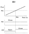
図1の送信回路は、例えば、GSMの広帯域伝送機能であるEDGE方式に適した移動体通信用送信機に使用されるものである。1は変調器であり、ベースバンド回路(図示略)から送信情報(ランプアップ信号や送信データ等)が入力され、送信信号や位相、振幅の変調信号を生成し、出力する。変調器1の位相(PM)信号が位相比較器2に送られ、ループフィルタ3を経た信号が高周波電力増幅器(以下、単に電力増幅器)4に送られる。また、電力増幅器4の出力情報がカプラーで検知され、ミキサ9、リミッタ増幅器11を経て位相情報が位相比較器2に帰還され、ここで変調器1の位相(PM)信号と比較され、その結果に基づいて位相調整された信号が電力増幅器へ送られる。5は振幅比較器、6はループフィルタである。電力増幅器4の出力情報がカプラーで検知され、ミキサ9、AM検波回路10を経て振幅情報が振幅比較器5に帰還され、これと変調器1の振幅(AM)信号との比較結果に基づいてループフィルタ6で振幅が補正され、電力増幅器4の制御入力側に入力される。7は切り替えスイッチであり、電力増幅器4のバイアス入力側を7−A又は7−Bに切り替える。8は切り替えスイッチで、変調器1のAM出力側を8−A又は8−Bに切り替える。9はミキサ、10はAM検波回路、11はリミッタ増幅器である。また、700は切り替え制御回路であり、電力増幅器4の出力を制御する送信情報と所定の閾値Pthとを比較し、切り替えスイッチ7、8を切り替えるための制御信号を出力する。すなわち、切り替え制御回路700及び切り替えスイッチ7、8は、送信回路の振幅(AM)制御ループを切り替えるための切り替え制御ユニットとして構成されている。
The transmission circuit of FIG. 1 is used for a mobile communication transmitter suitable for the EDGE system, which is a GSM broadband transmission function, for example.
切り替え制御回路700は、電力増幅器4の出力Pout(具体的には変調器1に入力される送信情報 Ramp Up )を所定の閾値Pth(より具体的には送信情報に対する閾値 Rth)と比較し、出力Poutが閾値Pthよりも小さい中低出力時(または低出力時)には、切り替えスイッチ7、8を共にA接点側、すなわち図1に実線で示した状態に切り替える。これに伴い、図2に示すように、送信回路の位相(PM)制御に関しては、電力増幅器4、カプラー、ミキサ9、リミッタ増幅器11、位相比較器2及びループフィルタ6を含む帰還回路が存在するが、振幅(AM)制御に関しては、振幅比較器5、ループフィルタ6を含む帰還回路がオープンとなるため、電力増幅器4が変調器1のAM出力信号に基づいて直接的にAM変調される開ループ制御となる。
The
一方、電力増幅器4の出力Pout(変調器1の送信情報)が所定の閾値Pthよりも大きな大出力時には、切り替えスイッチ7、8を共にB接点側に切り替える。これに伴い、電力増幅器4の出力がカプラー、ミキサ9、AM検波回路10を経て振幅比較器5に帰還され、これと変調器1の変調出力信号との比較結果に基づいてループフィルタ6で電力増幅器4の出力振幅が補正されるポーラループ回路が構成される。すなわち、送信回路の振幅(AM)制御に関しては、図2に示すように閉ループ制御となる。これにより、大電力時の送信回路は、2つの帰還回路により変調器1の変調信号が補正された振幅、位相に基づき電力増幅器4の出力電力が制御されるポーラループ送信回路となる。
On the other hand, when the output Pout of the power amplifier 4 (transmission information of the modulator 1) is a large output larger than the predetermined threshold value Pth, both the
このように本発明の実施例では、電力増幅器の非線形性の強い大電力時には振幅、位相2つの帰還回路が動作するポーラループ送信回路として動作させ、中低出力時には振幅を開ループ制御することで中低出力時の消費電流を削減する。また、電力増幅器の入力振幅―振幅特性、振幅―位相特性は出力電力の大小に拘わらず適正に保持される。 As described above, in the embodiment of the present invention, the power amplifier is operated as a polar loop transmission circuit in which the feedback circuit having two amplitudes and phases operates when the power amplifier has strong nonlinearity, and the amplitude is controlled by open loop control at the middle and low outputs. Reduce current consumption at medium to low output. Further, the input amplitude-amplitude characteristics and amplitude-phase characteristics of the power amplifier are appropriately maintained regardless of the magnitude of the output power.
なお、切り替えスイッチ7、8の実際の切り替えは、変調器1の送信情報中のランプアップデータと所定の閾値Rthとの比較により行なう。この特定の閾値Rthの設定に際しては、電力増幅器4の特性の変動を考慮して、若干の余裕を持たせるのが良い。また、用途に応じて、閾値Rthを選択、変更できるようにしておくのが望ましい。さらに、電力増幅器4の出力Poutに相当する他の情報を用い、それに対応する所定の閾値と比較するようにしても良い。
The actual switching of the
次に、図1の電力増幅器4の具体的な構成例と、その構成例における切り替えスイッチ7、8の切り替えのための所定の閾値Pth(もしくはRth)との関係について、説明する。
Next, a relationship between a specific configuration example of the
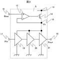
図3は、電力増幅器4の具体的な回路構成例の1つを示すものである。
この電力増幅器においては、電力制御を、電力増幅器4の電源で行うように、電力増幅器4の電源にレギュレータを用いている。すなわち、電力増幅器4は、オペレーション増幅器12、電源端子13、p形MOSFET14、内部電源端子15、バイアス制御入力端子16、入力端子17、出力端子18、初段増幅器19、2段目増幅器20、最終段増幅器21を備えている。電力制御のために、電力増幅器4の初段増幅器19、2段目増幅器20、最終段増幅器21に対する電源部として、電源端子13と、オペレーション増幅器12、p形MOSFET14、内部電源端子15及びバイアス制御入力端子16を含むレギュレータを備えている。
FIG. 3 shows one specific circuit configuration example of the
In this power amplifier, a regulator is used for the power source of the
図4は、図3に示した電力増幅器4と負荷インピーダンス(Z)29の関係を示す図である。電力増幅器4の負荷インピーダンスZは、アンテナの環境によって大きく変動する。
FIG. 4 is a diagram showing the relationship between the
本発明の送信回路では、パワーロスを低減するために、アイソレータを用いずに、アンテナの環境による変動の影響の低減を図るものである。特に、GSM方式では等振幅で位相変調した信号を要求出力レベルに応じて出力するので、電力増幅器は常に飽和領域で動作させることができるが、EDGE方式では、振幅にも情報を重畳する振幅制御を行なうために、使用環境の変動の如何にかかわらず電力増幅器を線形動作させるための工夫が必要である。そのために、本発明では、切り替えスイッチ7、8の動作点を、上記所定の閾値Pthとすることに1つの特徴がある。以下、この点について、説明する。 In the transmission circuit of the present invention, in order to reduce power loss, the influence of fluctuation due to the environment of the antenna is reduced without using an isolator. In particular, since the GSM system outputs a signal modulated in phase with equal amplitude according to the required output level, the power amplifier can always operate in the saturation region, but in the EDGE system, amplitude control that superimposes information on the amplitude as well. Therefore, it is necessary to devise a method for linearly operating the power amplifier regardless of changes in the usage environment. Therefore, the present invention has one feature in that the operating point of the changeover switches 7 and 8 is set to the predetermined threshold value Pth. Hereinafter, this point will be described.
図5は、本発明の第一の実施形態における図3の電力増幅器4の負荷インピーダンスの変動を示す特性図である。30は最大送信時の電力増幅器負荷線、31は、最大送信時でかつ負荷インピーダンスが小さい場合の電力増幅器負荷線、32は最大送信時でかつ負荷インピーダンスが大きい場合の電力増幅器負荷線である。
FIG. 5 is a characteristic diagram showing variations in load impedance of the
次に、図6は、本発明の第一の実施形態において、電源を変化させた場合の負荷インピーダンスの変動を示す図である。88は中出力送信時の電力増幅器負荷線を示す図である。33は中出力送信時で負荷インピーダンスが小さい場合の電力増幅器負荷線である。35は小出力送信時の電力増幅器負荷線、36は小出力送信時で負荷インピーダンスが小さい場合の電力増幅器負荷線である。34は内部電源電圧差分を示す。
Next, FIG. 6 is a diagram showing a change in load impedance when the power source is changed in the first embodiment of the present invention. 88 is a diagram showing a power amplifier load line at the time of medium output transmission.
この図から明らかな通り、中出力送信時あるいは小出力送信時で負荷インピーダンスが小さい場合の電力増幅器負荷線33、36は、いずれも電力増幅器4の飽和領域内にあり、開ループ制御により、電力増幅器4を変調器1の出力に基づいてAM変調制御することができる。しかし、最大送信時でかつ負荷インピーダンスが小さい場合は、その電力増幅器の負荷線31が、内部電源電圧差分34だけ飽和領域外に出る。そのため、開ループ制御により、電力増幅器4を変調器1の出力に基づいて正確にAM変調制御することができなくなる。
As is apparent from this figure, the power
そこで、本実施形態においては、最大送信時の電力増幅器の負荷線30を境に(実際には若干の余裕を持って)、負荷線30の右側は閉ループ制御すなわちポーラループの送信回路とし、左側は開ループ制御の送信回路に切り替えるものである。
Therefore, in this embodiment, the
図7は、本発明の第一の実施形態における、電力増幅器の出力と最大許容負荷変動量の関係を示す特性図である。本実施形態においては、切り替え制御回路700により、電力増幅器4の負荷変動時の大きな大送信時はポーラループ送信回路、負荷変動時の小さな中小出力電力時には開ループ制御の送信回路に切り替わる。これにより、図6で述べたことからも明らかな通り、電力増幅器4の負荷インピーダンスの大小にかかわらず、所定の最大許容負荷変動量を確保できるので、電力増幅器4を正確に制御することができる。また、中小出力送信時はAM開ループ制御とすることで、消費電流の少ない送信回路を提供することができる。
FIG. 7 is a characteristic diagram showing the relationship between the output of the power amplifier and the maximum allowable load fluctuation amount in the first embodiment of the present invention. In the present embodiment, the switching
次に、図8は、図1に示した第一の実施形態に用いる電力増幅器4の別の例を示すものである。この例では、電力増幅器4の電力制御を、電力増幅器4のゲートあるいはベースバイアスで行う。17は入力端子、18は出力端子、22は入力整合回路、23はHBTトランジスタ、24は抵抗、25は段間整合回路、26は出力整合回路、27はバイアス抵抗、28はバイアス回路を示す。
Next, FIG. 8 shows another example of the
図9は、図8のベースバイアス形電力増幅器4を採用した第一の実施形態において、電源を変化させた場合の負荷インピーダンスの変動を示す図である。300は最大送信時の電力増幅器負荷線、310は最大送信時でかつ負荷インピーダンスが小さい場合の電力増幅器負荷線、320は最大送信時でかつ負荷インピーダンスが大きい場合の電力増幅器負荷線である。37は増幅器の最大出力電力のバイアス点、38は増幅器の変調波の最大バイアス点、39は増幅器の変調波の最小バイアス点を示す。また、40は増幅器の負荷変動時の最大出力電力のバイアス点、41は増幅器の負荷変動時の最大出力電力変調波の最大のバイアス点、42は増幅器の負荷変動時の最大出力電力変調波の最小のバイアス点を示す。さらに、43は増幅器の中出力電力のバイアス点、44は増幅器の中出力電力変調波の最大バイアス点、45は増幅器の中出力電力変調波の最小バイアス点を示す。
FIG. 9 is a diagram showing the fluctuation of the load impedance when the power source is changed in the first embodiment employing the base bias
中出力電力時において、各バイアス点(43、44、45)は、線形性が保たれており、開ループ制御でも、ベースバイアス形電力増幅器4を変調器1の出力に基づいてAM変調制御することができる。
At the time of medium output power, each bias point (43, 44, 45) is kept linear, and the base bias
しかし、電力増幅器負荷線320で示した最大送信時でかつ負荷インピーダンスが大きい場合は、電力増幅器4の特性が飽和してしまい、制御が困難となる。すなわち、ベースバイアス形増幅器の負荷変動時の最大出力電力のバイアス点40、負荷変動時の最大出力電力変調波の最大のバイアス点41が、いずれも飽和状態にあり、電力増幅器4を変調器1の出力に基づいて正確にAM変調制御することができなくなる。一方、増幅器の負荷変動時の最大出力電力変調波の最小のバイアス点42は、制御可能な不飽和の領域にある。
However, when the maximum transmission shown by the power
そこで、本実施形態においては、所定の閾値Pthを境にして、ベースバイアス形増幅器のバイアスの大きい時すなわち大出力電力時はポーラループ送信回路とし、バイアスの小さい時すなわち中小出力電力時には開ループ制御の送信回路に切り替える。これにより、図9のバイアス点40、41での使用を避けることができ、電力増幅器4の負荷インピーダンスの大小にかかわらず、電力増幅器4を変調器1の出力に基づいて正確に制御することができる。また、中小出力送信時はAM開ループ制御とすることで、消費電流の少ない送信回路を提供することができる。
Therefore, in the present embodiment, with a predetermined threshold Pth as a boundary, a polar loop transmission circuit is used when the bias of the base bias type amplifier is large, that is, when the output power is large, and open loop control is performed when the bias is small, that is, when the output is medium or small. Switch to the transmitter circuit. Accordingly, use at the bias points 40 and 41 in FIG. 9 can be avoided, and the
本発明の第二の実施形態を図10〜図15で説明する。まず、図10は本発明の第二の実施形態になる送信回路の要部を示す図、図11は第二の実施形態の動作タイミング生成回路を示す図、図12は、第二の実施形態の動作タイミングを示す図、図13は第二の実施形態の動作説明図である。 A second embodiment of the present invention will be described with reference to FIGS. First, FIG. 10 is a diagram illustrating a main part of a transmission circuit according to the second embodiment of the present invention, FIG. 11 is a diagram illustrating an operation timing generation circuit according to the second embodiment, and FIG. 12 is a diagram illustrating the second embodiment. FIG. 13 is an operation explanatory diagram of the second embodiment.
図10において、1は変調器、46は位相比較器、3は送信用発信器及びフィルタ48を含むループフィルタ、4は電力増幅器、61はアンテナスイッチである。電力増幅器4は、多段接続されたヘテロバイポーラトランジスタ(HBT)、バイアス回路28、カップラ49、検波回路50、エラー増幅器51を備えている。また、位相ループもしくは振幅ループ中に配置された要素として、振幅比較器47、可変増幅器52、ステップ増幅器53、可変増幅器54、ループフィルタ55、電圧電流変換器56、フィルタ57、バッファ増幅器58、ミキサ60、電圧電流変換器62を備えている。ベースバンド回路から変調器1に入力された送信情報(ランプ信号や送信データ等)は、デジタルインターフェイス66を経てデジタルIQ変調器65に送られる。デジタルIQ変調器65のIQデータは局座標変換器67で局座標変換され、AM成分とPM成分の信号がDA変換器65及び直交変調器63を介して位相比較器46及び振幅比較器47に入力される。また、局座標変換器67で変換されたAM成分の信号はプリディストーション回路68で歪が補正され、DA変換器69を経てVramp信号となり、電力増幅器4の振幅がこの信号に比例した値に制御される。ベースバンド回路から変調器1に入力された送信情報(ランプ信号や送信データ等)は、送信データレジスタ70にも保持され、これらの情報を利用して切り替え制御回路700が切り替えスイッチ7、8及び切り替えスイッチ59の切り替え動作を制御する。切り替えスイッチ8の固定端子にはVramp信号が接続されている。切り替えスイッチ7及び8は、GSM側及びEDGE側の接点を有する。また、切り替えスイッチ59は、可変増幅器52側及びステップ増幅器53側の接点を有する。
In FIG. 10, 1 is a modulator, 46 is a phase comparator, 3 is a loop filter including a transmitter and a
図11は、第二の実施形態における、切り替えスイッチの動作タイミングを生成する切り替え制御ユニット、すなわち送信データレジスタ70及び切り替え制御回路700の構成例を示すものである。送信データレジスタ70は、8PSK、GMSK等の変調方式の情報を保持する変調方式識別レジスタ71、電力増幅器4の電力レベルに相当するランプ信号を保持するランプ信号レジスタ72、及び送信データを保持する送信データレジスタ73を保持している。切り替え制御回路700には、変調方式識別レジスタ1バースト分のデータ74、ランプ信号レジスタの1バースト内最大値75の情報が入力、保持される。76は開ループ、閉ループしきい値レジスタであり、予め設定された閾値Pthを保持している。77は比較器であり、電力増幅器4の電力レベルに相当するランプ信号と閾値Pthとの比較結果に基づき、1か0の値を出力する。78は比較結果を保持する比較結果レジスタである。79は論理積であり、データ74の変調方式と上記比較結果との論理積演算を行なう。論理積79の出力は、CLAとして開ループ、閉ループ設定レジスタ80に設定される。
FIG. 11 shows a configuration example of the switching control unit that generates the operation timing of the selector switch, that is, the transmission data register 70 and the switching
この移動体通信用送信回路で処理される通信方式は、通常の音声交信用に等振幅で位相に情報を乗せるGMSK変調方式を用いるGSM通信方式と、振幅にも情報を重畳する8―PSK(8相Phase Shift Keying)変調方式を用いるEDGE方式とに対応している。電力増幅器4は、これら両通信方式に対応し、送信回路の位相に関しては常に帰還回路が動作し、振幅に関しては、電力増幅器の出力に基づいて開ループまたはポーラループ制御のいずれかになる。
The communication system processed by the mobile communication transmission circuit includes a GSM communication system using a GMSK modulation system in which information is put on a phase with equal amplitude in normal voice communication, and 8-PSK ( This corresponds to the EDGE system using an 8-phase phase shift keying) modulation system. The
図12に第二の実施形態の動作タイミングを示す。
GSM通信方式では、送信信号がTX1〜TX4の4スロットで構成され、TX1〜TX3は8―PSK変調、TX4は等振幅のGMSKとなっている。電力増幅器4の振幅変調制御に関しては、8―PSKの振幅と所定の閾値Pthとの関係に応じて、電力増幅器が開ループまたはポーラループ制御のいずれかになる。
FIG. 12 shows the operation timing of the second embodiment.
In the GSM communication system, the transmission signal is composed of four slots TX1 to TX4, TX1 to TX3 is 8-PSK modulation, and TX4 is equal amplitude GMSK. With respect to the amplitude modulation control of the
図12のCLAは、閉ループ設定レジスタ80の出力を示しており、CLAが0のとき開ループ、1のときポーラループ制御となるように、各切り替えスイッチが切り替えられる。
CLA in FIG. 12 indicates the output of the closed
切り替え制御回路700は、電力増幅器4の送信電力(具体的には変調器1のランプ信号Rump )がある閾値レベル(具体的にはRumpに対応するRth )以上では振幅ループを閉ループ制御し、前記閾値レベル以下では開ループ制御するように、切り替えスイッチ7、8及び59を切り替えるための制御信号、例えば"AM−OPEN"を出力する。すなわち、切り替え制御回路700は、送信データレジスタ70から読み出された電力増幅器4の出力に対応するランプ信号と所定の閾値Pthとを、比較器77において比較する。そして、この比較結果を基にCLAを出力し、切り替えスイッチ7、8、59を切り替え、オープン制御または閉ループ制御を行なう。
The switching
TX1のスロットでは、8―PSK変調のため変調方式識別レジスタのデータ74が1にも拘わらず、電力増幅器4の送信電力は閾値レベル未満(LP)なので、論理積79は0となり、CLAが0(低)で開ループ制御となる。TX2〜TX3は8―PSK変調のため変調方式識別レジスタのデータ74が1であり、かつ、電力増幅器4の送信電力は閾値レベル以上(HP)なので、論理積79は1となり、CLAが1(高)で閉ループ制御となる。
In the slot of TX1, since the transmission power of the
TX4のGMSKについては、電力増幅器4の送信電力は閾値レベル以上(HP)であるが、一定振幅でよいので変調方式識別レジスタのデータ74が0となっており、論理積79は0となり、CLAが0で開ループ制御となる。
As for TX4 GMSK, the transmission power of the
このように、切り替え制御回路700は、電力増幅器4の中低出力時は、切り替えスイッチ7、8をGSM側、切り替えスイッチ59をステップ増幅器53側の接点に切り替える。このとき、位相情報は、デジタルIQ変調器65から直交変調器63を経て位相比較器46に入力され、ステップ増幅器53を経由した帰還情報と比較され、その結果に基づいてループフィルタ3で変調された信号が電力増幅器4に入力される。ステップ増幅器53は、利得の大まかな制御を行なうものであり可変増幅器52に比べて制御精度は低下するが、電力の消費が少ない利点がある。
As described above, the switching
一方、デジタルIQ変調器65から、局座標変換器67、プリディストーション回路68、DA変換器69を経て生成された振幅情報であるVramp信号は、切り替えスイッチ8、電圧電流変換器56、切り替えスイッチ7、ループフィルタ57、バッファ増幅器58を経て電力増幅器4のバイアス回路28に送られる。すなわち、位相は閉ループ、振幅はオープン制御となる。
On the other hand, the Vramp signal, which is amplitude information generated from the
電力増幅器4の大出力時は、CLAが1となり、切り替えスイッチ7、8をEDGE側、切り替えスイッチ59を可変増幅器52側の接点に切り替える。位相情報は、デジタルIQ変調器65から直交変調器63を経て位相比較器46に入力され、可変増幅器52を経由した帰還情報と比較され、その結果によってループフィルタで偏重された信号が電力増幅器4に入力される。一方、振幅情報であるVramp信号は、切り替えスイッチ8、可変増幅器54、電圧電流変換器62、切り替えスイッチ7、ループフィルタ57、バッファ増幅器58を経て変調され、電力増幅器4のバイアス回路28に送られる。すなわち、位相、振幅共に閉ループ制御となる。
At the time of high output of the
図13は、第2の実施形態における電力増幅器の大出力時、すなわち振幅変調でポーラループ制御されている時の動作を説明する図である。電力増幅器4の大出力時は、直交変調器63のIF変調波と可変増幅器52を経由した振幅帰還情報とが振幅比較器47に入力され、その出力である誤差信号がループフィルタ55で積分され、可変増幅器54で増幅して帰還をかけ、変調のかかった信号を電力増幅器4から発生させる。可変増幅器52の出力G1aがG1+ΔGのとき、可変増幅器54の出力G2aはG2−ΔGとなり、G1a+ΔG+G2a−ΔG=G1+G2=一定、となる。すなわち、可変増幅器52の出力の増減分を可変増幅器54でキャンセルすることで、ループ利得は一定値に保たれる。
FIG. 13 is a diagram for explaining the operation of the power amplifier according to the second embodiment at the time of large output, that is, when polar loop control is performed by amplitude modulation. When the
このようにして、ポーラループ制御時は、可変増幅器52と可変増幅器54とで、一種の固定増幅器が構成される。
Thus, during polar loop control, the
他方、電力増幅器4の中小出力電力時には、AM開ループ制御とする。すなわち、振幅情報であるVramp信号に基づき電力増幅器4の振幅制御がなされると共に、ステップ増幅器53を経て位相の帰還制御がなされる。これにより、可変増幅器52、振幅比較器47、可変増幅器52、可変増幅器54、電圧電流変換器62が非作動状態となり、消費電流の少ない送信回路を提供することができる。
On the other hand, when the output power of the
本実施形態では、切り替え制御回路700により、振幅レベルの変わる変調信号を出力するときでも、信号レベルに応じて正しく開ループ、閉ループの切り替えを行うことができる。
In this embodiment, even when the modulation signal whose amplitude level changes is output by the switching
以上述べたとおり、本実施形態では、電力増幅器の非線形性の強い大電力時には振幅と位相の2つの帰還回路が動作するポーラループ送信回路を動作させ、電力増幅器の線形性が確保される中低出力時には振幅を開ループ制御することで中低出力時の消費電流を削減することができる。 As described above, in this embodiment, when the power amplifier has high nonlinearity and high power, the polar loop transmission circuit in which two feedback circuits of amplitude and phase operate is operated to ensure the linearity of the power amplifier. By controlling the amplitude at the time of output, the current consumption at the time of medium and low output can be reduced.
このように、本発明の第2の実施形態では、電力増幅器の出力レベルに応じて、位相(PM)制御に関しては、可変増幅器52とステップ増幅器53とを切り替え、振幅(AM)制御は、開ループ、閉ループに切り替えている。この第2の実施形態における効果を、以下説明する。
まず、図14(A、B)で、本発明の第2の実施形態の位相歪について説明する。図14Aに位相歪のシミュレーション条件を示す。図14Aの(1)に示すように振幅 (AM−AM) 特性は線形とした。また、振幅、位相歪(AM−PM)特性については、図14Aの(2)、(3)に(a)〜(j)として示すように、1.00 deg/dBないし0.02 deg/dBを評価した。図14Bに位相歪のシミュレーション結果を示す。図14Bの(1)に示すように、振幅、位相歪特性は、(e)の0.20deg/dBでシステム規格を満たしている。しかし、EVM変調精度は、いずれもシステム規格(5%以下)を満たしていない。一方、図14Bの(2)に示すように、振幅、位相歪特性が、(f)〜(j)すなわち0.10deg/dBないし0.02 deg/dBの範囲では、EVM変調精度もシステム規格を満たしている。なお、(f)の0.1 deg/dBの付近はステップ増幅器53を用いた位相ループを有する送信回路であり、(j)の0.02 deg/dB以下の範囲がポーラループ送信回路の場合である。
Thus, in the second embodiment of the present invention, the phase (PM) control is switched between the
First, with reference to FIGS. 14A and 14B, the phase distortion of the second embodiment of the present invention will be described. FIG. 14A shows the simulation conditions for phase distortion. As shown in (1) of FIG. 14A, the amplitude (AM-AM) characteristic was linear. As for amplitude and phase distortion (AM-PM) characteristics, as shown in (2) and (3) of FIG. 14A as (a) to (j), 1.00 deg / dB to 0.02 deg / dB was evaluated. FIG. 14B shows the simulation result of the phase distortion. As shown in (1) of FIG. 14B, the amplitude and phase distortion characteristics satisfy the system standard at 0.20 deg / dB of (e). However, none of the EVM modulation accuracy satisfies the system standard (5% or less). On the other hand, as shown in (2) of FIG. 14B, when the amplitude and phase distortion characteristics are in the range of (f) to (j), that is, 0.10 deg / dB to 0.02 deg / dB, the EVM modulation accuracy is also the system standard. Meet. The vicinity of 0.1 deg / dB in (f) is a transmission circuit having a phase loop using the
次に、図15(A、B)で、本発明の第2の実施形態の振幅歪について説明する。図15Aに振幅歪のシミュレーション条件を示す。図15Aに示すように線形利得を(a)〜(f)として示すように、0.2 /dBないし0.005/dBの範囲で変化させた。図15Bにシミュレーション結果を示す。図15Bにおいて、(d)の0.02/dB以下の範囲で、システム規格を満たしている。すなわち、大出力時はポーラループ送信回路を動作させることで線形性が高まり、規格を満たすことができる。なお、中小出力時は、歪が小さくなるので、オープンループでもシステム規格を満たすことができる。 Next, with reference to FIGS. 15A and 15B, amplitude distortion according to the second embodiment of the present invention will be described. FIG. 15A shows simulation conditions for amplitude distortion. As shown in FIG. 15A, the linear gain was changed in the range of 0.2 / dB to 0.005 / dB as shown as (a) to (f). FIG. 15B shows the simulation result. In FIG. 15B, the system standard is satisfied within the range of 0.02 / dB of (d). That is, when the output is large, the linearity is increased by operating the polar loop transmission circuit, and the standard can be satisfied. In addition, since the distortion becomes small at the time of medium and small outputs, the system standard can be satisfied even in an open loop.
すなわち、本実施形態に示したように、電力増幅器の非線形性の強い大電力時には振幅と位相の2つの帰還回路が動作するポーラループ送信回路を動作させ、中小出力時は開ループ制御とすることで、広い出力範囲にわたりシステム規格を満たすことができる。 That is, as shown in this embodiment, the polar loop transmission circuit in which two feedback circuits of amplitude and phase are operated when the power amplifier has strong nonlinearity and the power is large, and the open loop control is performed when the output is small and medium. Therefore, system standards can be satisfied over a wide output range.
以上述べたように、大送信時はポーラループ送信回路、中小出力電力時には開ループ制御の送信回路に切り替えるものである。これにより、電力増幅器4の負荷インピーダンスの大小にかかわらず、電力増幅器4を変調器1の出力に基づいて正確に制御することができる。また、中小出力送信時はAM開ループ制御とすることで、消費電流の少ない送信回路を提供することができる。
As described above, the switching is made to the polar loop transmission circuit at the time of large transmission, and to the transmission circuit of the open loop control at the time of medium to small output power. Thereby, the
本発明の第三の実施形態を図16、図17に示す。図16は、本発明の第三の実施形態になる送信回路を示す図であり、図17は、本実施形態の動作タイミング生成回路である。この実施形態では、第一の実施形態と異なり、RF(高周波)ICの内部でかつ、ループフィルタ3と電力増幅器4との間にバッファアンプ400が追加され、このバッファアンプ400に並列にバイバススィッチ410が接続されている。また、帰還信号も、RFICの内部でかつバッファアンプ400の出力側から取得される。さらに、ミキサ9の出力を電力増幅器4の制御入力側もしくはバッファアンプ400の入力側に切り替えるための切り替えスイッチ420が、RF(高周波)ICの内部に設けられている。切り替え制御回路700は、切り替えスイッチ7、8に加えて、バイバススィッチ410、420を切り替えるための制御信号を出力する。なお、電力増幅器4の出力制御は、RFICの外部の回路で行なわれる。
A third embodiment of the present invention is shown in FIGS. FIG. 16 is a diagram illustrating a transmission circuit according to the third embodiment of the present invention, and FIG. 17 is an operation timing generation circuit according to the present embodiment. In this embodiment, unlike the first embodiment, a
図17に本実施形態の動作タイミングを示す。電力増幅器4の振幅変調制御に関しては、8―PSKの振幅と所定の閾値Pthとの関係に応じて、電力増幅器が開ループまたはポーラループ制御のいずれかになる。GMSKについては、FM変調信号は不要であり、開ループ制御となる。図17のCLAは、閉ループ設定レジスタ80の出力を示しており、CLAが0のとき開ループ、1のときポーラループ制御となるように、各切り替えスイッチが切り替えられる。また、PABが0すなわちTX1〜TX3の8―PSKの振幅変調時、バイバススィッチ410は開でかつ、ミキサ9の出力は電力増幅器4の制御入力側に加えられる。PABが1すなわちTX4のGMSKのとき、バイバススィッチ420がバッファアンプ400の入力側に切り替えられ、かつ、バイバススィッチ410が閉じられる。
FIG. 17 shows the operation timing of this embodiment. With respect to the amplitude modulation control of the
本実施形態によれば、FM変調信号が全て単一のRFICの内部で生成、処理されるため、ノイズの発生が少なくなる。従って、バッファアンプ400と電力増幅器4の間に、ノイズ除去用のフィルターを設ける必要は無く、コストを低減できる。
According to this embodiment, since all FM modulation signals are generated and processed inside a single RFIC, the generation of noise is reduced. Therefore, it is not necessary to provide a noise removing filter between the
図18は、本発明の第四の実施形態になる送信回路の要部を示す図である。 FIG. 18 is a diagram showing a main part of a transmission circuit according to the fourth embodiment of the present invention.
この実施形態では、位相ループにオフセット送信機を用いている点が特徴である。図18において、ループフィルタ3、電力増幅器4、リミッタ増幅器81、可変分周器82、位相比較器46、及びリファレンス信号源83を含む位相ループが構成されている。送信信号はベースバンドICのデジタルインターフェイス66を介してデジタルIQ変調器65に入力され、局座標変換器67で変換されたPM成分がデルタ、シグマ変調器84を経て基準クロックの逓数倍の高い周波数に調整されて可変分周器82の制御入力に加えられ、可変分周器82によりリミッタ増幅器81の出力をオフセットする。このオフセットされた帰還信号が位相比較器46においてリファレンス信号源83からのリファレンス信号と比較されて位相制御信号となり、これに基づき電力増幅器4の位相が制御される。振幅制御に関する構成は、本発明の第二の実施形態と同じであるので、説明を省略する。
This embodiment is characterized in that an offset transmitter is used for the phase loop. In FIG. 18, a phase loop including the
この実施形態では、位相ループにオフセット送信機を用いて安定な動作を実現することができる。位相ループにデルタシグマ送信機を用い、ミキサを省略することで、一層の低電力化を測ることができる。 In this embodiment, stable operation can be realized by using an offset transmitter in the phase loop. By using a delta-sigma transmitter in the phase loop and omitting the mixer, further reduction in power can be measured.
本発明の送信回路は、例えば、GSM方式の広帯域伝送機能であるEDGE方式に適した移動体通信用の無線通信装置に適用できる。この場合、無線通信装置の送信部は、既に述べた実施例になる送信回路を備えており、例えば、高周波電力増幅モジュールと、利得可変(AGC)増幅器を有する高周波ICと、バイアス制御部を備えている。高周波電力増幅モジュールは、既に述べた実施例の電力増幅器4、A/D変換器、バイアス制御回路などがMMIC(Microwave Monolithic IC)として、1つのセラミック基板上に実装されている。出力制御部を有するベースバンド制御回路の一部も、送信部を構成する。ベースバンド制御回路は、GSM方式やEDGE方式の信号の変調や復調を行なうことができる変復調回路や送信データ(ベースバンド信号)に基づいてI,Q信号を生成したり受信信号から抽出されたI,Q信号を処理するベースバンド回路と、送信信号から高調波成分を除去するバンドパスフィルタ(BPF1)、受信信号から不要波を除去するバンドパスフィルタ(BPF2)などが1つのパッケージに実装されている。
The transmission circuit of the present invention can be applied to, for example, a wireless communication apparatus for mobile communication suitable for the EDGE system, which is a GSM broadband transmission function. In this case, the transmission unit of the wireless communication apparatus includes the transmission circuit according to the above-described embodiment, and includes, for example, a high frequency power amplification module, a high frequency IC having a variable gain (AGC) amplifier, and a bias control unit. ing. In the high-frequency power amplification module, the
本実施例によれば、電力増幅器の入力振幅―振幅特性、振幅―位相特性が出力電力の大小に拘わらず適正に保持され、かつ、消費電流の少ない送信回路を備えた、移動体通信用の無線通信装置を提供することができる。 According to the present embodiment, the input amplitude-amplitude characteristics and the amplitude-phase characteristics of the power amplifier are appropriately maintained regardless of the magnitude of the output power, and equipped with a transmission circuit with low current consumption, for mobile communication. A wireless communication device can be provided.
1…変調器、2…位相比較器、3…ループフィルタ、4…電力増幅器、5…振幅比較器、6…ループフィルタ、7…切り替えスイッチ、8…切り替えスイッチ、9…ミキサ、10…AM検波回路、11…リミッタ増幅器、12…オペレーション増幅器、13…電源端子、14…p形MOSFET、15…内部電源端子、16…バイアス制御入力端子、17…入力端子、18…出力端子、19…初段増幅器、20…2段目増幅器、21…最終段増幅器、22…入力整合回路、23…HBTトランジスタ、25…段間整合回路、26…出力整合回路、27…バイアス抵抗、28…バイアス回路、29…負荷インピーダンス、30…電力増幅器負荷線(最大送信時)、31…電力増幅器負荷線(最大送信時で負荷インピーダンスが小さい場合)、32…電力増幅器負荷線(最大送信時で負荷インピーダンスが大きい場合)、88…電力増幅器負荷線(中出力送信時)、33…電力増幅器負荷線(中出力送信時で負荷インピーダンスが小さい場合),34…内部電源電圧差分、35…電力増幅器負荷線(小出力送信時)、36…電力増幅器負荷線(小出力送信時で負荷インピーダンスが小さい場合)37…ベースバイアス形増幅器の最大出力電力のバイアス点、38…ベースバイアス形の変調波の最大バイアス点、39…ベースバイアス形の変調波の最小バイアス点、40…ベースバイアス形増幅器の負荷変動時の最大出力電力のバイアス点、41…ベースバイアス形増幅器の負荷変動時の最大出力電力変調波の最大のバイアス点、42…ベースバイアス形増幅器の負荷変動時の最大出力電力変調波の最小のバイアス点、43…ベースバイアス形増幅器の中出力電力のバイアス点、44…ベースバイアス形増幅器の中出力電力変調波の最大バイアス点、45…ベースバイアス形増幅器の中出力電力変調波の最小バイアス点、46…位相比較器、47…振幅比較器、48…ループフィルタ。49…カップラ。50…検波回路。51…エラー増幅器、52…可変増幅器。53…ステップ増幅器、54…可変増幅器、55…ループフィルタ、56…電圧電流変換器、57…フィルタ、58…バッファ増幅器、59…切り替えスイッチ、60…ミキサ、61…アンテナスイッチ、62…電圧電流変換器、63…直交変調器、64…DA変換器、65…デジタルIQ変調器、66…デジタルインターフェイス、67…局座標変換器、68…プリディストーション回路、69…DA変換器、70…送信データレジスタ、71…変調方式識別レジスタ、72…ランプ信号レジスタ、73…送信データ、74…変調方式識別レジスタ1バースト分、75…ランプ信号レジスタの1バースト内最大値、76…開ループ、閉ループしきい値レジスタ、77…比較器、78…比較結果レジスタ、79…論理積、80…開ループ、閉ループ設定レジスタ、81…リミッタ増幅器、82…可変分周器、83…リファレンス信号源、84…デルタ、シグマ変調器、85…信号源、86…シンセサイザ、87…バッファアンプ、115…アンテナ、400…バッファアンプ、410…バイバススィッチ、420…切り替えスイッチ切り替え、700…切り替え制御回路。
DESCRIPTION OF
Claims (20)
前記振幅ループを閉ループ又は開ループのいずれかに切り替える切り替え制御ユニットを備え、
前記切り替え制御ユニットは、前記電力増幅器の大出力時には前記振幅ループを閉ループとし、前記電力増幅器の低出力時には前記振幅ループを開ループとすることを特徴とする送信回路。 A phase loop for controlling the phase of the transmission output of the power amplifier, and an amplitude loop for controlling the amplitude of the transmission output of the power amplifier,
A switching control unit for switching the amplitude loop to either a closed loop or an open loop;
The transmission control circuit, wherein the switching control unit sets the amplitude loop to a closed loop when the power amplifier has a high output, and sets the amplitude loop to an open loop when the power amplifier has a low output.
前記電力増幅器の大出力時は、前記位相ループ及び前記振幅ループからなるポーラループ送信回路を構成し、
前記電力増幅器の低出力時には、前記振幅ループを開ループとし、前記位相ループのみ閉ループに維持することを特徴とする送信回路。 In claim 1,
At the time of large output of the power amplifier, a polar loop transmission circuit composed of the phase loop and the amplitude loop is configured,
A transmission circuit characterized in that when the power amplifier has a low output, the amplitude loop is an open loop, and only the phase loop is maintained in a closed loop.
前記位相ループは、前記電力増幅器、第一のループフィルタ、リミッタ増幅器、および位相比較器を含んで構成され、
前記振幅ループは、前記電力増幅器、AM検波回路、振幅比較器及び第二のループフィルタを含む回路として構成され、前記電力増幅器の大出力時には前記振幅ループが閉成されて変調器の出力信号と帰還信号に基づいてAM変調を行ない、前記電力増幅器の低出力時には前記振幅ループが前記AM検波回路、前記振幅比較器及び前記第二のループフィルタを含まない開ループとし前記変調器の出力信号に基づいてAM変調を行なうことを特徴とする送信回路。 In claim 1,
The phase loop includes the power amplifier, a first loop filter, a limiter amplifier, and a phase comparator,
The amplitude loop is configured as a circuit including the power amplifier, an AM detection circuit, an amplitude comparator, and a second loop filter. When the power amplifier has a large output, the amplitude loop is closed and the output signal of the modulator is AM modulation is performed based on a feedback signal, and the amplitude loop is an open loop that does not include the AM detection circuit, the amplitude comparator, and the second loop filter when the output of the power amplifier is low. A transmission circuit characterized by performing AM modulation based on the above.
前記切り替え制御ユニットは、前記電力増幅器の制御入力側を前記変調器および前記振幅ループの第二のループフィルタのいずれか一方に接続する第一の切り替えスイッチと、前記変調器を前記第一の切り替えスイッチおよび前記振幅比較器のいずれか一方に接続する第二の切り替えスイッチと、前記電力増幅器の出力レベルを与える送信情報に基づいて前記第一の切り替えスイッチ及び前記第二の切り替えスイッチを切り替える切り替え制御回路とを備えていることを特徴とする送信回路。 In claim 3,
The switching control unit includes a first changeover switch that connects a control input side of the power amplifier to one of the modulator and a second loop filter of the amplitude loop, and the first changeover of the modulator. A second changeover switch connected to one of the switch and the amplitude comparator, and a changeover control for changing over the first changeover switch and the second changeover switch based on transmission information giving an output level of the power amplifier And a transmission circuit.
前記振幅ループを閉ループ又は開ループのいずれかに切り替える切り替え制御ユニットを備え、
前記切り替え制御ユニットは、前記送信出力が所定の閾値よりも大きい範囲では前記振幅ループを閉ループとし、前記送信出力が前記閾値よりも小さい範囲では前記振幅ループを開ループ制御とすることを特徴とする送信回路。 A phase loop for controlling the phase of the transmission output, and an amplitude loop for controlling the amplitude of the transmission output,
A switching control unit for switching the amplitude loop to either a closed loop or an open loop;
The switching control unit sets the amplitude loop to a closed loop when the transmission output is larger than a predetermined threshold, and sets the amplitude loop to open loop control when the transmission output is smaller than the threshold. Transmitter circuit.
前記所定の閾値は、送信回路の電力増幅器の大出力時と低出力時とを識別するための閾値であり、
前記切り替え制御ユニットは、前記閾値と送信情報に含まれる前記電力増幅器の出力レベルを示す信号とを比較し、前記振幅ループを閉ループ又は開ループのいずれかに切り替えることを特徴とする送信回路。 In claim 5,
The predetermined threshold is a threshold for distinguishing between a high output and a low output of the power amplifier of the transmission circuit,
The switching control unit compares the threshold and a signal indicating the output level of the power amplifier included in transmission information, and switches the amplitude loop to either a closed loop or an open loop.
前記送信回路は、EDGE方式の通信規格に対応するものであり、前記送信情報に含まれる前記電力増幅器の出力電力レベルを示すランプ信号を前記出力レベルを示す信号として用いることを特徴とする送信回路。 In claim 6,
The transmission circuit corresponds to an EDGE communication standard, and uses a ramp signal indicating the output power level of the power amplifier included in the transmission information as a signal indicating the output level. .
前記電力増幅器の電力制御を、該電力増幅器の電源で行なうように、前記電力増幅器の電源にレギュレータを用いることを特徴とする送信回路。 In claim 6,
A transmission circuit using a regulator as a power source of the power amplifier so that power control of the power amplifier is performed by the power source of the power amplifier.
前記電力増幅器の電力制御を、該電力増幅器のゲートバイアスおよびベースバイアスのいずれか一方で行うことを特徴とする送信回路。 In claim 6,
A transmission circuit characterized in that power control of the power amplifier is performed by one of a gate bias and a base bias of the power amplifier.
前記電力増幅器の大出力時は、前記位相ループ及び前記振幅ループからなるポーラループ送信回路を構成し、
前記電力増幅器の低出力時には、前記振幅ループを開ループとし、前記位相ループのみ閉ループに維持することを特徴とする送信回路。 In claim 6,
At the time of large output of the power amplifier, a polar loop transmission circuit composed of the phase loop and the amplitude loop is configured,
A transmission circuit characterized in that when the power amplifier has a low output, the amplitude loop is an open loop, and only the phase loop is maintained in a closed loop.
前記位相ループがオフセットPLLであることを特徴とする送信回路。 In claim 5,
The transmission circuit, wherein the phase loop is an offset PLL.
前記位相ループ及び前記振幅ループの両ループフィルタと電力増幅器との間にバッファアンプが接続され、該バッファアンプの出力側から前記位相ループ及び前記振幅ループへの帰還信号を取得することを特徴とする送信回路。 In claim 5,
A buffer amplifier is connected between both loop filters of the phase loop and the amplitude loop and a power amplifier, and a feedback signal to the phase loop and the amplitude loop is obtained from the output side of the buffer amplifier. Transmitter circuit.
前記位相ループは、前記電力増幅器、第一のループフィルタ、可変増幅器、および位相比較器を含んで構成され、
前記振幅ループは、前記電力増幅器、AM検波回路、振幅比較器及び第二のループフィルタを含んで構成され、
前記送信情報に基づき前記振幅ループを閉ループ又は開ループのいずれかに切り替える切り替え制御ユニットを備え、
該切り替え制御ユニットは、前記電力増幅器の制御入力側を前記変調器もしくは前記第二のループフィルタのいずれかに接続する第一の切り替えスイッチと、前記変調器を前記第一の切り替えスイッチもしくは前記振幅比較器のいずれかに接続する第二の切り替えスイッチと、前記電力増幅器の出力レベルに基づいて前記第一の切り替えスイッチ及び前記第二の切り替えスイッチを切り替える切り替え制御回路とを備え、
前記切り替え制御ユニットは、前記電力増幅器の大出力時には前記振幅ループを閉ループとし、前記電力増幅器の低出力時には前記振幅ループが前記AM検波回路、前記振幅比較器及び前記第二のループフィルタを含まない開ループとすることを特徴とする移動体通信用送信機。 A power amplifier, a modulator for outputting a phase control signal and an amplitude control signal for controlling the power amplifier based on transmission information, a phase loop for controlling a phase of a transmission output of the power amplifier by the phase control signal, A transmitter for mobile communication comprising a transmission circuit including an amplitude loop for controlling an amplitude of a transmission output of the power amplifier based on the amplitude control signal;
The phase loop includes the power amplifier, a first loop filter, a variable amplifier, and a phase comparator,
The amplitude loop includes the power amplifier, an AM detection circuit, an amplitude comparator, and a second loop filter,
A switching control unit that switches the amplitude loop to either a closed loop or an open loop based on the transmission information,
The switching control unit includes a first changeover switch that connects a control input side of the power amplifier to either the modulator or the second loop filter, and the modulator to the first changeover switch or the amplitude. A second changeover switch connected to one of the comparators, and a changeover control circuit for changing over the first changeover switch and the second changeover switch based on the output level of the power amplifier,
The switching control unit is configured such that the amplitude loop is closed when the power amplifier has a large output, and the amplitude loop does not include the AM detection circuit, the amplitude comparator, and the second loop filter when the power amplifier has a low output. A transmitter for mobile communication characterized by being an open loop.
前記位相ループは、第一の切り替えスイッチを介して前記可変増幅器と並列に配置されたステップ増幅器を有し、
前記切り替え制御ユニットは、前記電力増幅器の大出力時には前記可変増幅器を前記位相ループの構成要素とし、前記電力増幅器の低出力時には前記ステップ増幅器を前記位相ループの構成要素とすることを特徴とする移動体通信用送信機。 In claim 13,
The phase loop has a step amplifier arranged in parallel with the variable amplifier via a first changeover switch;
The switching control unit has the variable amplifier as a component of the phase loop when the power amplifier has a large output, and the step amplifier as a component of the phase loop when the power amplifier has a low output. Transmitter for body communication.
前記振幅ループは、前記電力増幅器に設けられたカプラー、第一の可変増幅器、前記振幅比較器、第二の可変増幅器、第一の電流電圧変換器及び前記第二のループフィルタからなる回路と、第二の切り替えスイッチを介して前記第一の可変増幅器及び前記第一の電流電圧変換器に対して並列に配置された第二の可変増幅器及び第二の電流電圧変換器とを有し、
前記切り替え制御ユニットは、前記電力増幅器の大出力時には、前記電力増幅器、前記カプラー、前記第一の可変増幅器、前記振幅比較器、前記第一の電流電圧変換器及び前記第二のループフィルタからなる回路を前記振幅ループの構成要素とし、前記電力増幅器の低出力時には、前記電力増幅器、前記カプラー、第二の可変増幅器、前記振幅比較器、及び前記ループフィルタからなる回路を前記振幅ループの構成要素とすることを特徴とする移動体通信用送信機。 In claim 13,
The amplitude loop is a circuit comprising a coupler provided in the power amplifier, a first variable amplifier, the amplitude comparator, a second variable amplifier, a first current-voltage converter, and the second loop filter; A second variable amplifier and a second current-voltage converter arranged in parallel to the first variable amplifier and the first current-voltage converter via a second changeover switch;
The switching control unit includes the power amplifier, the coupler, the first variable amplifier, the amplitude comparator, the first current-voltage converter, and the second loop filter when the power amplifier has a large output. A circuit is a component of the amplitude loop, and the circuit including the power amplifier, the coupler, the second variable amplifier, the amplitude comparator, and the loop filter at the time of low output of the power amplifier is a component of the amplitude loop. A transmitter for mobile communication characterized by the above.
前記位相ループは、前記電力増幅器に設けられたカプラーと前記位相比較器の間に接続されたリミッタ増幅器と、該リミッタ増幅器の出力をオフセットする可変分周器を有することを特徴とする移動体通信用送信機。 In claim 13,
The phase loop includes a limiter amplifier connected between a coupler provided in the power amplifier and the phase comparator, and a variable frequency divider for offsetting the output of the limiter amplifier. Transmitter.
前記位相ループにデルタシグマ送信機を用いたことを特徴とする移動体通信用送信機。 In claim 16,
A transmitter for mobile communication, wherein a delta-sigma transmitter is used for the phase loop.
前記第一、第二のループフィルタと前記電力増幅器との間にバッファアンプが接続され、該バッファアンプの出力側に設けられた第二のカプラーから前記位相ループ及び前記振幅ループへの帰還信号を取得するように構成され、
前記第一のループフィルタ、前記可変増幅器、及び前記位相比較器と、前記振幅ループの前記AM検波回路、前記振幅比較器及び前記第二のループフィルタと、前記バッファアンプ及び前記第二のカプラーが、共通のRFIC上に設けられていることを特徴とする移動体通信用送信機。 In claim 13,
A buffer amplifier is connected between the first and second loop filters and the power amplifier, and a feedback signal from the second coupler provided on the output side of the buffer amplifier to the phase loop and the amplitude loop. Configured to get and
The first loop filter, the variable amplifier, and the phase comparator, the AM detection circuit of the amplitude loop, the amplitude comparator and the second loop filter, the buffer amplifier, and the second coupler. A transmitter for mobile communication, which is provided on a common RFIC.
前記切り替え制御ユニットは、送信データレジスタを備えており、該送信データレジスタは、8PSK、GMSK等の変調方式の情報を保持する変調方式識別レジスタ、前記電力増幅器の電力レベルに相当するランプ信号を保持するランプ信号レジスタ、及び送信データを保持する送信データレジスタを有していることを特徴とする移動体通信用送信機。 In claim 13,
The switching control unit includes a transmission data register. The transmission data register holds a modulation scheme identification register that holds modulation scheme information such as 8PSK and GMSK, and a ramp signal corresponding to the power level of the power amplifier. A transmitter for mobile communication, comprising: a ramp signal register that performs transmission and a transmission data register that retains transmission data.
前記切り替え制御ユニットは、切り替え制御回路を備えており、
前記切り替え制御回路は、前記送信データレジスタから読み出された前記電力増幅器の出力に対応するランプ信号と所定の閾値とを、比較器において比較し、この比較結果を基に前記切り替えスイッチを切り替えて、オープン制御または閉ループ制御を行なうことを特徴とする移動体通信用送信機。 In claim 19,
The switching control unit includes a switching control circuit,
The switching control circuit compares a ramp signal corresponding to the output of the power amplifier read from the transmission data register with a predetermined threshold in a comparator, and switches the switching switch based on the comparison result. A mobile communication transmitter characterized by performing open control or closed loop control.
Priority Applications (2)
| Application Number | Priority Date | Filing Date | Title |
|---|---|---|---|
| JP2006151762A JP4676383B2 (en) | 2006-05-31 | 2006-05-31 | Transmitter circuit and transmitter for mobile communication using the same |
| US11/755,273 US7873333B2 (en) | 2006-05-31 | 2007-05-30 | Transmitter circuits and apparatus of wireless application |
Applications Claiming Priority (1)
| Application Number | Priority Date | Filing Date | Title |
|---|---|---|---|
| JP2006151762A JP4676383B2 (en) | 2006-05-31 | 2006-05-31 | Transmitter circuit and transmitter for mobile communication using the same |
Publications (3)
| Publication Number | Publication Date |
|---|---|
| JP2007324846A JP2007324846A (en) | 2007-12-13 |
| JP2007324846A5 JP2007324846A5 (en) | 2008-12-25 |
| JP4676383B2 true JP4676383B2 (en) | 2011-04-27 |
Family
ID=38790889
Family Applications (1)
| Application Number | Title | Priority Date | Filing Date |
|---|---|---|---|
| JP2006151762A Expired - Fee Related JP4676383B2 (en) | 2006-05-31 | 2006-05-31 | Transmitter circuit and transmitter for mobile communication using the same |
Country Status (2)
| Country | Link |
|---|---|
| US (1) | US7873333B2 (en) |
| JP (1) | JP4676383B2 (en) |
Families Citing this family (21)
| Publication number | Priority date | Publication date | Assignee | Title |
|---|---|---|---|---|
| JP2006135422A (en) * | 2004-11-02 | 2006-05-25 | Matsushita Electric Ind Co Ltd | Transmission circuit |
| US8107902B2 (en) * | 2005-11-28 | 2012-01-31 | Paragon Communications Ltd. | Method and apparatus for optimizing current consumption of amplifiers with power control |
| JP4799494B2 (en) * | 2007-07-02 | 2011-10-26 | パナソニック株式会社 | Transmitter |
| US8588351B2 (en) * | 2007-08-22 | 2013-11-19 | Motorola Mobility Llc | Multi-band signal detection |
| DE102007061453B4 (en) * | 2007-12-20 | 2015-07-23 | Intel Mobile Communications GmbH | Method for calibrating a transmitter and radio transmitter |
| WO2009100408A2 (en) | 2008-02-08 | 2009-08-13 | Skyworks Solutions, Inc. | Closed-loop adaptive power control for adjusting bandwidth in a mobile handset transmitter |
| US8489046B2 (en) * | 2008-07-21 | 2013-07-16 | Panasonic Corporation | Signal decomposition methods and apparatus for multi-mode transmitters |
| US7970360B2 (en) * | 2008-10-24 | 2011-06-28 | Harris Corporation | Electronic device with a distortion correction circuit for a power amplifier, and associated methods |
| US8249531B2 (en) * | 2008-10-31 | 2012-08-21 | Apple, Inc. | Transmit power measurement and control methods and apparatus |
| US8422968B2 (en) * | 2009-06-03 | 2013-04-16 | Apple Inc. | Wireless electronic device with open-loop and closed-loop output power control |
| US8219145B2 (en) * | 2009-09-03 | 2012-07-10 | Micro Mobio Corporation | Universal radio card for wireless devices |
| US8688901B2 (en) | 2009-12-08 | 2014-04-01 | Intel Corporation | Reconfigurable load-reduced memory buffer |
| US8487705B2 (en) | 2010-05-26 | 2013-07-16 | Triquint Semiconductor, Inc. | Protection circuit for radio frequency power amplifier |
| US20130044836A1 (en) * | 2011-08-18 | 2013-02-21 | Vyycore Ltd. | Device and method for pre-distorting and amplifying a signal based on an error attribute |
| US20130113559A1 (en) * | 2011-11-08 | 2013-05-09 | Vyycore Ltd. | Device and method for pre-distorting and amplifying a signal based on an error attribute |
| US8538368B1 (en) * | 2011-11-14 | 2013-09-17 | Triquint Semiconductor, Inc. | Dynamic power limiter circuit |
| US9595924B2 (en) * | 2012-08-03 | 2017-03-14 | Broadcom Corporation | Calibration for power amplifier predistortion |
| JP2014036388A (en) * | 2012-08-09 | 2014-02-24 | Sharp Corp | Transmitter, program, and storage medium thereof |
| DE102013201653A1 (en) * | 2013-01-31 | 2014-07-31 | Intel Mobile Communications GmbH | SWITCHING AND MOBILE COMMUNICATION DEVICE |
| MX349316B (en) | 2013-08-19 | 2017-07-21 | Arris Entpr Llc | Fiber-optic node with forward data content driven power consumption. |
| US9667312B2 (en) * | 2015-01-13 | 2017-05-30 | Hughes Network Systems, Llc | Radio based automatic level control for linear radio calibration |
Citations (3)
| Publication number | Priority date | Publication date | Assignee | Title |
|---|---|---|---|---|
| WO2003009481A1 (en) * | 2001-07-17 | 2003-01-30 | Mitsubishi Denki Kabushiki Kaisha | Transmission power control circuit |
| JP2004007446A (en) * | 2002-05-31 | 2004-01-08 | Renesas Technology Corp | Semiconductor integrated circuit for communication, wireless communication apparatus, transmission apparatus, and transmission start method |
| JP2005520457A (en) * | 2002-05-29 | 2005-07-07 | シーメンス アクチエンゲゼルシヤフト | Circuit arrangement for switching a mobile radio transmitter between two modulation modes |
Family Cites Families (2)
| Publication number | Priority date | Publication date | Assignee | Title |
|---|---|---|---|---|
| US6295442B1 (en) * | 1998-12-07 | 2001-09-25 | Ericsson Inc. | Amplitude modulation to phase modulation cancellation method in an RF amplifier |
| GB0212740D0 (en) * | 2002-05-31 | 2002-07-10 | Hitachi Ltd | Transmitter and wireless communication apparatus using the transmitter |
-
2006
- 2006-05-31 JP JP2006151762A patent/JP4676383B2/en not_active Expired - Fee Related
-
2007
- 2007-05-30 US US11/755,273 patent/US7873333B2/en not_active Expired - Fee Related
Patent Citations (3)
| Publication number | Priority date | Publication date | Assignee | Title |
|---|---|---|---|---|
| WO2003009481A1 (en) * | 2001-07-17 | 2003-01-30 | Mitsubishi Denki Kabushiki Kaisha | Transmission power control circuit |
| JP2005520457A (en) * | 2002-05-29 | 2005-07-07 | シーメンス アクチエンゲゼルシヤフト | Circuit arrangement for switching a mobile radio transmitter between two modulation modes |
| JP2004007446A (en) * | 2002-05-31 | 2004-01-08 | Renesas Technology Corp | Semiconductor integrated circuit for communication, wireless communication apparatus, transmission apparatus, and transmission start method |
Also Published As
| Publication number | Publication date |
|---|---|
| JP2007324846A (en) | 2007-12-13 |
| US7873333B2 (en) | 2011-01-18 |
| US20070281652A1 (en) | 2007-12-06 |
Similar Documents
| Publication | Publication Date | Title |
|---|---|---|
| JP4676383B2 (en) | Transmitter circuit and transmitter for mobile communication using the same | |
| EP1710918B1 (en) | Transmitter and wireless communication apparatus | |
| US7062236B2 (en) | Transmitter circuits | |
| US7817970B2 (en) | Transmitting/receiving device having a polar modulator with variable predistortion | |
| US8548400B2 (en) | System and method for polar modulation using power amplifier bias control | |
| US7560984B2 (en) | Transmitter | |
| JP5437511B2 (en) | High frequency amplifier circuit and mobile communication terminal using the same | |
| EP1880475B1 (en) | Amplitude calibration element for an enhanced data rates for gsm evolution (edge) polar loop transmitter | |
| US7792214B2 (en) | Polar modulation transmitter circuit and communications device | |
| EP2037587B1 (en) | Transmission circuit and communication device | |
| EP2055061B1 (en) | Replica linearized power amplifier | |
| US5422598A (en) | High-frequency power amplifier device with drain-control linearizer circuitry | |
| US8417199B2 (en) | Method and apparatus for improving efficiency in a power supply modulated system | |
| JP2000165264A (en) | Power consumption reduction circuit at transmission, radio communication terminal using it and linear operation control method | |
| EP2056479A1 (en) | Transmission circuit and communication apparatus | |
| JP2008048397A (en) | Circuit structure and method for setting analog output signal | |
| US7395036B2 (en) | Semiconductor integrated circuit for high frequency power amplifier and electric components with the semiconductor integrated circuit | |
| KR100927650B1 (en) | Transmitter for mobile communication terminal and its transmission method | |
| JP2007174553A (en) | Electronic component for high-frequency power amplification, and wireless communication apparatus | |
| US7940859B2 (en) | Transmission circuit and communication device | |
| JP2008017453A (en) | Radio frequency amplifier circuit, and mobile communication terminal using the same | |
| JP2005217562A (en) | High frequency power amplifier circuit | |
| Warr et al. | A 60% PAE WCDMA handset transmitter amplifier | |
| JP2006121408A (en) | Modulation signal transmitting circuit and radio communication equipment | |
| EP4293897A2 (en) | Doherty power amplifier system |
Legal Events
| Date | Code | Title | Description |
|---|---|---|---|
| A521 | Written amendment |
Free format text: JAPANESE INTERMEDIATE CODE: A523 Effective date: 20081107 |
|
| A621 | Written request for application examination |
Free format text: JAPANESE INTERMEDIATE CODE: A621 Effective date: 20081107 |
|
| A711 | Notification of change in applicant |
Free format text: JAPANESE INTERMEDIATE CODE: A712 Effective date: 20100510 |
|
| A977 | Report on retrieval |
Free format text: JAPANESE INTERMEDIATE CODE: A971007 Effective date: 20101228 |
|
| TRDD | Decision of grant or rejection written | ||
| A01 | Written decision to grant a patent or to grant a registration (utility model) |
Free format text: JAPANESE INTERMEDIATE CODE: A01 Effective date: 20110111 |
|
| A01 | Written decision to grant a patent or to grant a registration (utility model) |
Free format text: JAPANESE INTERMEDIATE CODE: A01 |
|
| A61 | First payment of annual fees (during grant procedure) |
Free format text: JAPANESE INTERMEDIATE CODE: A61 Effective date: 20110127 |
|
| FPAY | Renewal fee payment (event date is renewal date of database) |
Free format text: PAYMENT UNTIL: 20140204 Year of fee payment: 3 |
|
| R150 | Certificate of patent or registration of utility model |
Free format text: JAPANESE INTERMEDIATE CODE: R150 |
|
| S531 | Written request for registration of change of domicile |
Free format text: JAPANESE INTERMEDIATE CODE: R313531 |
|
| R350 | Written notification of registration of transfer |
Free format text: JAPANESE INTERMEDIATE CODE: R350 |
|
| LAPS | Cancellation because of no payment of annual fees |