EP3035407A2 - Anzeigevorrichtung - Google Patents
Anzeigevorrichtung Download PDFInfo
- Publication number
- EP3035407A2 EP3035407A2 EP15200430.5A EP15200430A EP3035407A2 EP 3035407 A2 EP3035407 A2 EP 3035407A2 EP 15200430 A EP15200430 A EP 15200430A EP 3035407 A2 EP3035407 A2 EP 3035407A2
- Authority
- EP
- European Patent Office
- Prior art keywords
- layer
- thin film
- display device
- substrate
- film encapsulation
- Prior art date
- Legal status (The legal status is an assumption and is not a legal conclusion. Google has not performed a legal analysis and makes no representation as to the accuracy of the status listed.)
- Granted
Links
Images


Classifications
-
- H—ELECTRICITY
- H10—SEMICONDUCTOR DEVICES; ELECTRIC SOLID-STATE DEVICES NOT OTHERWISE PROVIDED FOR
- H10K—ORGANIC ELECTRIC SOLID-STATE DEVICES
- H10K59/00—Integrated devices, or assemblies of multiple devices, comprising at least one organic light-emitting element covered by group H10K50/00
- H10K59/60—OLEDs integrated with inorganic light-sensitive elements, e.g. with inorganic solar cells or inorganic photodiodes
-
- H—ELECTRICITY
- H10—SEMICONDUCTOR DEVICES; ELECTRIC SOLID-STATE DEVICES NOT OTHERWISE PROVIDED FOR
- H10F—INORGANIC SEMICONDUCTOR DEVICES SENSITIVE TO INFRARED RADIATION, LIGHT, ELECTROMAGNETIC RADIATION OF SHORTER WAVELENGTH OR CORPUSCULAR RADIATION
- H10F77/00—Constructional details of devices covered by this subclass
- H10F77/40—Optical elements or arrangements
- H10F77/413—Optical elements or arrangements directly associated or integrated with the devices, e.g. back reflectors
-
- H—ELECTRICITY
- H10—SEMICONDUCTOR DEVICES; ELECTRIC SOLID-STATE DEVICES NOT OTHERWISE PROVIDED FOR
- H10F—INORGANIC SEMICONDUCTOR DEVICES SENSITIVE TO INFRARED RADIATION, LIGHT, ELECTROMAGNETIC RADIATION OF SHORTER WAVELENGTH OR CORPUSCULAR RADIATION
- H10F77/00—Constructional details of devices covered by this subclass
- H10F77/50—Encapsulations or containers
-
- H—ELECTRICITY
- H10—SEMICONDUCTOR DEVICES; ELECTRIC SOLID-STATE DEVICES NOT OTHERWISE PROVIDED FOR
- H10K—ORGANIC ELECTRIC SOLID-STATE DEVICES
- H10K50/00—Organic light-emitting devices
- H10K50/80—Constructional details
- H10K50/84—Passivation; Containers; Encapsulations
- H10K50/842—Containers
- H10K50/8426—Peripheral sealing arrangements, e.g. adhesives, sealants
-
- H—ELECTRICITY
- H10—SEMICONDUCTOR DEVICES; ELECTRIC SOLID-STATE DEVICES NOT OTHERWISE PROVIDED FOR
- H10K—ORGANIC ELECTRIC SOLID-STATE DEVICES
- H10K50/00—Organic light-emitting devices
- H10K50/80—Constructional details
- H10K50/84—Passivation; Containers; Encapsulations
- H10K50/844—Encapsulations
- H10K50/8445—Encapsulations multilayered coatings having a repetitive structure, e.g. having multiple organic-inorganic bilayers
-
- H—ELECTRICITY
- H10—SEMICONDUCTOR DEVICES; ELECTRIC SOLID-STATE DEVICES NOT OTHERWISE PROVIDED FOR
- H10K—ORGANIC ELECTRIC SOLID-STATE DEVICES
- H10K50/00—Organic light-emitting devices
- H10K50/80—Constructional details
- H10K50/85—Arrangements for extracting light from the devices
- H10K50/856—Arrangements for extracting light from the devices comprising reflective means
-
- H—ELECTRICITY
- H10—SEMICONDUCTOR DEVICES; ELECTRIC SOLID-STATE DEVICES NOT OTHERWISE PROVIDED FOR
- H10K—ORGANIC ELECTRIC SOLID-STATE DEVICES
- H10K50/00—Organic light-emitting devices
- H10K50/80—Constructional details
- H10K50/85—Arrangements for extracting light from the devices
- H10K50/858—Arrangements for extracting light from the devices comprising refractive means, e.g. lenses
-
- H—ELECTRICITY
- H10—SEMICONDUCTOR DEVICES; ELECTRIC SOLID-STATE DEVICES NOT OTHERWISE PROVIDED FOR
- H10K—ORGANIC ELECTRIC SOLID-STATE DEVICES
- H10K59/00—Integrated devices, or assemblies of multiple devices, comprising at least one organic light-emitting element covered by group H10K50/00
- H10K59/10—OLED displays
- H10K59/12—Active-matrix OLED [AMOLED] displays
- H10K59/121—Active-matrix OLED [AMOLED] displays characterised by the geometry or disposition of pixel elements
-
- H—ELECTRICITY
- H10—SEMICONDUCTOR DEVICES; ELECTRIC SOLID-STATE DEVICES NOT OTHERWISE PROVIDED FOR
- H10K—ORGANIC ELECTRIC SOLID-STATE DEVICES
- H10K59/00—Integrated devices, or assemblies of multiple devices, comprising at least one organic light-emitting element covered by group H10K50/00
- H10K59/10—OLED displays
- H10K59/12—Active-matrix OLED [AMOLED] displays
- H10K59/13—Active-matrix OLED [AMOLED] displays comprising photosensors that control luminance
-
- H—ELECTRICITY
- H10—SEMICONDUCTOR DEVICES; ELECTRIC SOLID-STATE DEVICES NOT OTHERWISE PROVIDED FOR
- H10K—ORGANIC ELECTRIC SOLID-STATE DEVICES
- H10K59/00—Integrated devices, or assemblies of multiple devices, comprising at least one organic light-emitting element covered by group H10K50/00
- H10K59/80—Constructional details
- H10K59/84—Parallel electrical configurations of multiple OLEDs
-
- H—ELECTRICITY
- H10—SEMICONDUCTOR DEVICES; ELECTRIC SOLID-STATE DEVICES NOT OTHERWISE PROVIDED FOR
- H10K—ORGANIC ELECTRIC SOLID-STATE DEVICES
- H10K59/00—Integrated devices, or assemblies of multiple devices, comprising at least one organic light-emitting element covered by group H10K50/00
- H10K59/80—Constructional details
- H10K59/86—Series electrical configurations of multiple OLEDs
-
- H—ELECTRICITY
- H10—SEMICONDUCTOR DEVICES; ELECTRIC SOLID-STATE DEVICES NOT OTHERWISE PROVIDED FOR
- H10K—ORGANIC ELECTRIC SOLID-STATE DEVICES
- H10K59/00—Integrated devices, or assemblies of multiple devices, comprising at least one organic light-emitting element covered by group H10K50/00
- H10K59/80—Constructional details
- H10K59/87—Passivation; Containers; Encapsulations
- H10K59/873—Encapsulations
- H10K59/8731—Encapsulations multilayered coatings having a repetitive structure, e.g. having multiple organic-inorganic bilayers
-
- H—ELECTRICITY
- H10—SEMICONDUCTOR DEVICES; ELECTRIC SOLID-STATE DEVICES NOT OTHERWISE PROVIDED FOR
- H10K—ORGANIC ELECTRIC SOLID-STATE DEVICES
- H10K2102/00—Constructional details relating to the organic devices covered by this subclass
- H10K2102/301—Details of OLEDs
- H10K2102/351—Thickness
-
- H—ELECTRICITY
- H10—SEMICONDUCTOR DEVICES; ELECTRIC SOLID-STATE DEVICES NOT OTHERWISE PROVIDED FOR
- H10K—ORGANIC ELECTRIC SOLID-STATE DEVICES
- H10K59/00—Integrated devices, or assemblies of multiple devices, comprising at least one organic light-emitting element covered by group H10K50/00
- H10K59/80—Constructional details
- H10K59/875—Arrangements for extracting light from the devices
- H10K59/878—Arrangements for extracting light from the devices comprising reflective means
Definitions
- the described technology generally relates to a display device.
- LCDs liquid crystal displays
- OLED organic light-emitting diode
- EPDs electrophoretic displays
- PDPs plasma display panels
- LCDs LCDs, OLED displays, and EPDs are being developed into flexible display devices, and some of them have been implemented as cubic image display devices.
- pixels each of which is a basic unit of image expression, are arranged on a substrate in a matrix form, and a thin film transistor (TFT) is included in each pixel to independently control the pixel.
- TFT thin film transistor
- Such OLED displays may be classified into top-emission type display devices and bottom-emission type display devices according to the direction in which light is emitted.
- One inventive aspect relates to a display device.
- Another aspect is a display device that includes a substrate; a display unit formed on the substrate; a thin film encapsulation formed on an upper surface of the substrate to cover the display unit; an encapsulation substrate formed on an upper surface of the thin film encapsulation to encapsulate the display unit; and a photosensor on one end of the thin film encapsulation.
- the thin film encapsulation may include a plurality of organic layers and a plurality of inorganic layers which are alternately stacked.
- the plurality of organic layers and the plurality of inorganic layers may have different refractive indices from each other.
- a total reflection of light may repeatedly occur within the thin film encapsulation and the reflected light travels sideways.
- the display device may further include an adhesion layer between the thin film encapsulation and the encapsulation substrate, the adhesion layer attaching the thin film encapsulation to the encapsulation substrate.
- the adhesion layer may include metal particles.
- a reflection layer may be formed on an upper surface of the adhesion layer.
- Another aspect is a display device that includes a substrate having a light-emitting region and an outer region; an encapsulation substrate formed opposite the substrate; a display unit formed in the light-emitting region of the substrate; a thin film encapsulation formed on an upper surface of the substrate to cover the display unit; and a photosensor in the outer region of the substrate.
- the thin film encapsulation may include a plurality of organic layers and a plurality of inorganic layers which are alternately stacked.
- the plurality of organic layers and the plurality of inorganic layers may have different refractive indices from each other.
- a total reflection of light may repeatedly occur within the thin film encapsulation and the reflected light travels sideways.
- the photosensor may be formed on a lateral surface of the thin film encapsulation.
- the display device may further include an adhesion layer between the thin film encapsulation and the encapsulation substrate, the adhesion layer attaching the thin film encapsulation to the encapsulation substrate.
- the adhesion layer may include a transparent organic material.
- the adhesion layer may include metal particles.
- a reflection layer may be formed on an upper surface of the adhesion layer.
- Another aspect is a display device comprising: a substrate; a display unit formed over the substrate; a thin film encapsulation layer covering the display unit; an encapsulation substrate formed over the thin film encapsulation layer and encapsulating the display unit; and a photosensor formed on an end of the thin film encapsulation layer.
- the thin film encapsulation layer comprises a plurality of organic layers and a plurality of inorganic layers which are alternately stacked.
- the organic layers and the inorganic layers may have different refractive indices from each other.
- the reflected light is configured to travel sideways.
- the above display device may further comprise an adhesion layer formed between the thin film encapsulation layer and the encapsulation substrate, wherein the adhesion layer attaches the thin film encapsulation layer to the encapsulation substrate.
- the adhesion layer is formed of a transparent organic material.
- the adhesion layer may comprise a plurality of metal particles.
- the above display device further comprises a reflection layer formed over an upper surface of the adhesion layer.
- the thickness of the photosensor may be substantially the same as the combined thickness of the thin film encapsulation layer, the adhesion layer and the encapsulation substrate.
- the photosensor contacts lateral surfaces of the thin film encapsulation layer, the adhesion layer and the encapsulation substrate.
- a display device comprising: a substrate including a light-emitting region and an outer region; an encapsulation substrate formed opposite the substrate; a display unit formed in the light-emitting region of the substrate; a thin film encapsulation layer covering the display unit; and a photosensor formed in the outer region of the substrate.
- the thin film encapsulation layer may comprise a plurality of organic layers and a plurality of inorganic layers which are alternately stacked.
- the organic layers and the inorganic layers have different refractive indices from each other.
- the photosensor may be formed on a lateral surface of the thin film encapsulation layer.
- the above display device further comprises an adhesion layer formed between the thin film encapsulation layer and the encapsulation substrate, wherein the adhesion layer attaches the thin film encapsulation layer to the encapsulation substrate.
- the thickness of the photosensor may be substantially the same as the combined thickness of the thin film encapsulation layer, the adhesion layer and the encapsulation substrate.
- the photosensor contacts lateral surfaces of the thin film encapsulation layer, the adhesion layer and the encapsulation substrate.
- a display device comprising: a substrate; a display unit formed over the substrate and configured to output light; a thin film encapsulation layer covering the display unit; and a photosensor contacting a lateral surface of the thin film encapsulation layer and configured to sense at least part of the light output from the display unit.
- the above display device may further comprise an encapsulation substrate formed over the thin film encapsulation layer and encapsulating the display unit, wherein the photosensor contacts a lateral surface of the encapsulation substrate.
- the thickness of the photosensor may be greater than the combined thickness of the thin film encapsulation layer and the encapsulation substrate.
- the term “and/or” includes any and all combinations of one or more of the associated listed items. Expressions such as “at least one of” when preceding a list of elements, modify the entire list of elements and do not modify the individual elements of the list. In this disclosure, the term “substantially” includes the meanings of completely, almost completely or to any significant degree under some applications and in accordance with those skilled in the art.
- the term “connected” can include an electrical connection.
- FIG. 1 is a cross-sectional view of a display unit 20 according to an embodiment
- FIG. 2 is a cross-sectional view of a display device including the display unit of FIG. 1 according to an embodiment.
- the display device includes a substrate 10, the display unit 20, a thin film encapsulation layer 30, an encapsulation substrate 50, and a photosensor 60.
- the substrate 10 can be formed of a transparent glass material containing SiO 2 as a main component.
- the material used to form the substrate 10 is not limited thereto in embodiments of the invention, and the substrate 10 can be formed of a transparent plastic material.
- the display unit 20 will now be described in more detail with reference to FIG. 1 .
- a semiconductor layer A of a thin film transistor TFT is formed on the buffer layer 21.
- the semiconductor layer A may be formed of polysilicon and may include a channel region undoped with impurities and a source region and a drain region which are doped with impurities and are respectively formed both sides of the channel region.
- the impurities may vary depending on the type of thin film transistor, and may be N-type impurities or P-type impurities.
- the semiconductor layer A may be formed of a semiconductor including amorphous silicon or crystal silicon, and may be deposited using any of various deposition methods.
- the crystal silicon may be formed by crystallizing amorphous silicon.
- Amorphous silicon may be crystallized using any of various methods, such as rapid thermal annealing (RTA), solid phase crystallization (SPC), excimer laser annealing (ELA), metal induced crystallization (MIC), metal induced lateral crystallization (MILC), and sequential lateral solidification (SLS).
- RTA rapid thermal annealing
- SPC solid phase crystallization
- EVA excimer laser annealing
- MIC metal induced crystallization
- MILC metal induced lateral crystallization
- SLS sequential lateral solidification
- the semiconductor layer A may be patterned by photolithography.
- a gate insulating layer 23 is deposited on the entire surface of the substrate 10 such that its covers the semiconductor layer A.
- the gate insulating layer 23 may be formed of an inorganic material, such as silicon oxide or silicon nitride, and have a multilayer structure or single-layer structure.
- the gate insulating layer 23 may be formed of silicon nitride (SiN x ), silicon oxide (SiO2), hafnium (Hf) oxide, or aluminum oxide.
- the gate insulating layer 23 may be formed using any of various deposition methods, such as Chemical Vapour Deposition (CVD) and Plasma Enhanced Chemical Vapour Deposition (PECVD).
- the gate insulating layer 23 insulates the semiconductor layer A from a gate electrode G.
- An interlayer insulating layer 25 is deposited on the entire surface of the substrate 10 such that its covers the gate electrode G.
- the interlayer insulating layer 25 may be formed of an inorganic material or an organic material.
- the interlayer insulating layer 25 may be formed of an inorganic material.
- the interlayer insulating layer 25 may be formed of metal oxide or metal nitride.
- the inorganic material may include silicon oxide (SiO 2 ), silicon nitride (SiN x ), silicon oxynitride (SiON), aluminum oxide (Al2O3), titanium oxide (TiO2), tantalum oxide (Ta2O5), hafnium oxide (HfO2), zirconium oxide (ZrO2), or the like.
- the interlayer insulating layer 25 may be formed of an inorganic material, such as silicon oxide (SiOx) and/or silicon nitride (SiN x ), in a multi-layered or single-layered structure.
- the interlayer insulating layer 25 may have a double-layer structure of SiOx/SiNy or SiNx/SiOy.
- the interlayer insulating layer 25 may be formed using any of various deposition methods, such as CVD and PECVD.
- a source electrode S and a drain electrode D of the thin film transistor TFT are formed on the interlayer insulating layer 25.
- a planarization layer 27 can be formed on substantially the entire surface of the substrate 10 such that its covers the source electrode S and the drain electrode D.
- a pixel electrode 281 may be formed on the planarization layer 27. The pixel electrode 281 is connected to the drain electrode D of the thin film transistor TFT through a via hole.
- the planarization layer 27 can be formed of an insulating material.
- the planarization layer 27 can be formed of an inorganic material, an organic material, or an organic/inorganic compound in a single-layer or multilayer structure, and may be formed using any of various deposition methods.
- the planarization layer 27 may be formed of at least one selected from the group consisting of polyacrylates resin, epoxy resin, phenolic resin, polyamides resin, polyimides resin, unsaturated polyesters resin, poly phenylenethers resin, poly phenylenesulfides resin, and benzocyclobutene (BCB).
- OLED organic light-emitting diode
- the OLED includes the pixel electrode 281, an intermediate layer 283 including an organic emission layer, and an opposite electrode 285.
- the display device according to the present embodiment may further include a pixel defining layer 29 and a spacer (not shown).
- the pixel electrode 281 may be electrically connected to the drain electrode D of the thin film transistor TFT by filling the via hole of the planarization layer 27.
- the pixel electrode 281 and/or the opposite electrode 285 may be transparent electrodes or reflective electrodes.
- the pixel electrode 281 and/or the opposite electrode 285 may be formed of a material selected from the group consisting of indium tin oxide (ITO), indium zinc oxide (IZO), zinc oxide (ZnO), and indium oxide (In2O3).
- the pixel electrode 281 and/or the opposite electrode 285 may include a reflective layer that is formed of a material selected from the group consisting of silver (Ag), magnesium (Mg), aluminum (Al), platinum (Pt), palladium (Pd), gold (Au), nickel (Ni), neodymium (Nd), iridium (Ir), chromium (Cr), and a combination thereof, and a transparent layer that is formed of a material selected from the group consisting of ITO, IZO, ZnO, and In 2 O 3 .
- the pixel electrode 281 or the opposite electrode 285 may have an ITO/Ag/ITO structure.
- the pixel defining layer 29 may define a pixel region and a non-pixel region.
- the pixel defining layer 29 includes an aperture via which the pixel electrode 281 is exposed, and may be formed to cover the entire surface of the substrate 10.
- the intermediate layer 283, which will be described later, may be formed in the aperture, and thus the aperture may serve as a substantial pixel region.
- the pixel electrode 281, the intermediate layer 283, and the opposite electrode 285 constitute the OLED. Holes and electrons injected into the pixel electrode 281 and the opposite electrode 285 of the OLED may combine with each other in the organic emission layer of the intermediate layer 283 to thereby generate light.
- the intermediate layer 283 may include an organic emission layer.
- the intermediate layer 283 includes an organic emission layer.
- the intermediate layer 283 may further include at least one selected from a hole injection layer (HIL), a hole transport layer (HTL), an electron transport layer (ETL), and an electron injection layer (EIL).
- HIL hole injection layer
- HTL hole transport layer
- ETL electron transport layer
- EIL electron injection layer
- the present embodiment is not limited thereto, and the intermediate layer 283 may further include the other functional layers in addition to an organic emission layer.
- the HIL may be formed of a phthalocyanine compound such as copper phthalocyanine, or TCTA, m-MTDATA, or m-MTDAPB which is a star-bust type amine.
- a phthalocyanine compound such as copper phthalocyanine, or TCTA, m-MTDATA, or m-MTDAPB which is a star-bust type amine.
- the HTL may be formed of N,N'-bis(3-methylphenyl)-N,N'-diphenyl-[1,1-biphenyl]-4,4'-diamine (TPD), N,N'-di(naphthalene-1-yl)-N,N'-diphenyl benzidine ( ⁇ -NPD), and the like.
- TPD N,N'-bis(3-methylphenyl)-N,N'-diphenyl-[1,1-biphenyl]-4,4'-diamine
- ⁇ -NPD N,N'-di(naphthalene-1-yl)-N,N'-diphenyl benzidine
- the EIL may be formed of a material such as LiF, NaCl, CsF, Li 2 O, BaO, or Liq.
- the ETL may be formed of Alq 3 .
- the organic emission layer may include a host material and a dopant material.
- Examples of the host material of the organic emission layer may include tris 8-hydroxy-quinolinato)aluminum (Alq3, 9,10-di(naphth-2-yl)anthracene (AND), 3-tert-butyl-9,10-di(naphth-2-yl)anthracene (TBADN), 4,4'-bis 2,2-diphenyl-ethene-1-yl)-4,4'-dimethylphenyl (DPVBi), 4,4'-bis 2,2-diphenyl-ethene-1-yl)-4,4'-dimethylphenyl (p-DMDPVBi), tert 9,9-diarylfluorene)s (TDAF), 2- 9,9'-spirobifluorene-2-yl)-9,9'-spirobifluorene(BSDF), 2,7-bis 9,9'-spirobifluorene
- Examples of the dopant material of the organic emission layer may include 4,4'-bis[4-(di-p-tolylamino)styryl]biphenyl (DPAVBi), 9,10-di(naph-2-tyl)anthracene (ADN), 3-tert-butyl-9,10-di(naph-2-tyl)anthracene (TBADN), and the like.
- DPAVBi 4,4'-bis[4-(di-p-tolylamino)styryl]biphenyl
- ADN 9,10-di(naph-2-tyl)anthracene
- TAADN 3-tert-butyl-9,10-di(naph-2-tyl)anthracene
- the opposite electrode 285 is formed on the intermediate layer 283.
- the opposite electrode 285 forms an electric field together with the pixel electrode 281 so that light is emitted by the intermediate layer 283.
- the pixel electrode 281 may be patterned in each pixel, and the opposite electrode 285 may be formed so that a common voltage is applied to all of the pixels.
- the pixel electrode 281 and the opposite electrode 285 may be formed as transparent electrodes or as reflective electrodes.
- the pixel electrode 281 may function as an anode and the opposite electrode 285 may function as a cathode, but embodiments of the present invention are not limited thereto.
- the pixel electrode 281 may function as a cathode, and the opposite electrode 285 may function as an anode.
- the intermediate layer 283 may be commonly formed on the entire surface of the pixel electrode 281 regardless of locations of the pixels.
- the organic emission layer may be formed by stacking a light-emitting substance emitting a red light, a light-emitting substance emitting a green light, and a light-emitting substance emitting a blue light on one another or by mixing a light-emitting substance emitting a red light, a light-emitting substance emitting a green light, and a light-emitting substance emitting a blue light. Any combination of other various colors, which is capable of emitting a white light, may be employed in addition to a combination of red, green, and blue colors.
- the display device may further include a color converting layer or a color filter that coverts the white light into a light of a predetermined color.
- the spacer (not shown) may be formed between pixel regions in a display region, The spacer may maintain an interval between the substrate 10 and the encapsulation substrate 50 and prevent degradation of the display characteristics by external impacts.
- the spacer may be formed on the pixel defining layer 29.
- the spacer may protrude from the pixel defining layer 29 toward the encapsulation substrate 50.
- the spacer may include the same material as the pixel defining layer 29 and may be formed by using the same process as the process for forming the pixel defining layer 29.
- the pixel defining layer 29 and the spacer may be substantially simultaneously or concurrently formed by adjusting the amount of exposure by using a halftone mask during an exposure process.
- embodiments of the present invention are not limited thereto.
- the pixel defining layer 29 and the spacer may be sequentially or independently formed, and may be independent structures formed of different materials.
- the display device according to the present embodiment may be divided into a light-emitting region A, in which the display unit 20 emits light, and an outer region B, which is a remaining region of the display device.
- the light-emitting region A may include the above-described display unit 20 as illustrated in FIG. 2 .
- the thin film encapsulation or thin film encapsulation layer 30 may be formed on the substrate 10 such that it covers the display unit 20.
- FIG. 3 is a cross-sectional view illustrating the thin film encapsulation layer 30 in more detail, according to an embodiment.
- the thin film encapsulation 30 may be formed on the substrate 10 such that it covers the display unit 20.
- the thin film encapsulation 30 may have a structure in which a plurality of thin film layers are stacked.
- the thin film encapsulation 30 may have a structure in which an organic layer 31 and an inorganic layer 33 are alternately stacked.
- first organic layer 31a a first organic layer 31a, a first inorganic layer 33a, a second organic layer 31b, and a second inorganic layer 33b are sequentially stacked on the display unit 20 in FIG. 3
- the number of thin film layers that are stacked is not limited thereto in embodiments of the invention.
- the inorganic layer 33 may firmly block the penetration of oxygen or moisture, and the organic layer 31 may absorb stress generated by the inorganic layer 33 so that the thin film encapsulation may be flexible.
- the inorganic layer 33 may be a single layer or a layer stack including metal oxide or metal nitride.
- the first and second inorganic layers 33a and 33b may include SiN x , Al 2 O 3 , SiO 2 , or TiO 2 .
- the organic layer 31 may include a polymer and may be a single layer or a layer stack including polyethylene terephthalate, polyimide, polycarbonate, epoxy, polyethylene, or polyacrylate.
- the first and second organic layers 31a and 31b may be formed of polyacrylate.
- the first and second organic layers 31a and 31b may include a result of polymerizing a monomer composition including diacrylate-based monomer and triacrylate-based monomer.
- the monomer composition may further include monoacrylate-based monomer.
- the monomer composition may further include a well-known photoinitiator such as trimethyl benzoyl diphenyl phosphine oxide (TPO), but embodiments of the present invention are not limited thereto.
- TPO trimethyl benzoyl diphenyl phosphine oxide
- the thin film encapsulation 30 is formed to have a structure in which the organic layer 31 and the inorganic layer 33 are alternately stacked, penetration of oxygen and moisture may be prevented and also flexibility may be secured, and moreover total reflection may be controlled to smoothly occur within the thin film encapsulation 30.
- the organic layer 31 and the inorganic layer 33 are formed of materials having different refractive indices, light emitted by the display unit 20 is not discharged from the outer region B, and reflection repeatedly occurs within the thin film encapsulation 30.
- a conventional display device of a top-emission type does not include a structure corresponding to the thin film encapsulation 30 according to the present embodiment, and thus light loss occurs in the outer region B. Accordingly, the amount of light transmitted to a photosensor is not sufficient and thus the photosensor cannot sense light.
- the thin film encapsulation 30 is formed on the substrate 10 so that light emitted toward a top side of the display device may be reflected by the organic layer 31 and the inorganic layer 33 of the thin film encapsulation 30 in the outer region B and be confined within the thin film encapsulation 30.
- the thin film encapsulation 30 may further block, along with the encapsulation substrate 50, the display unit 20 from external oxygen and/or moisture.
- the thin film encapsulation 30 may confine light therewithin so that the light is not emitted to the top side, and may protect the display unit 20 from the outside.
- the photosensor 60 may be included in the outer region B.
- the photosensor 60 is formed on one end of the thin film encapsulation 30.
- the photosensor 60 may be implemented by using a photodiode, but embodiments of the present invention are not limited thereto.
- the photosensor 60 senses light and converts energy of the sensed light into electrical energy.
- the photosensor 60 is usually used in electronic products and may be employed to accurately measure the intensity of light. Since an output voltage may be generated according to the intensity of sensed light, the photosensor 60 may measure the intensity of light.
- a photosensor is attached directly to an upper surface the encapsulation substrate or a lower surface of the substrate and receives the reflected light.
- the encapsulation substrate does not have a total reflection control capability, and accordingly the photosensor receives weak light and thus is not expected to function as a sensor.
- the thin film encapsulation 30 since the thin film encapsulation 30 is included as illustrated in FIG. 2 , light is reflected by the organic layer 31 and the inorganic layer 33 of the thin film encapsulation 30 and travels sideways. Since the photosensor 60 is formed on one end of the thin film encapsulation 30, a sufficient amount of light may be transmitted to the photosensor 60.
- the photosensor 60 since the photosensor 60 is formed on one end of the thin film encapsulation 30, the photosensor 60 may receive a sufficient amount of light from the lateral side of the thin film encapsulation 30. Additionally, since the photosensor 60 is formed in an empty space within the outer region B, a practical use of a space may increase.
- the encapsulation substrate 50 may be formed opposite the substrate 10 in order to protect the display unit 20 included in the substrate 10 from external moisture, air, and the like.
- the encapsulation substrate 50 may be formed of the same material as the substrate 10, for example, a transparent glass or plastic material.
- the thin film encapsulation 30 and the encapsulation substrate 50, which are formed on the display unit 20, may additionally prevent the display unit 20 from penetration of external moisture, air, and the like.
- an adhesion layer 40 may be further formed between the thin film encapsulation 30 and the encapsulation substrate 50.
- the adhesion layer 40 may be located between respective ends of the thin film encapsulation 30 and the encapsulation substrate 50 as illustrated in FIG. 2 and seal the thin film encapsulation 30 and the encapsulation substrate 50.
- the adhesion layer 40 may include an organic material, such as epoxy, acryl, or silicon, including a light curing material, or an organic and inorganic material in which talc, Ca oxide (CaO), barium oxide (BaO), zeolite, SiO, or the like is included in an organic material.
- the adhesion layer 40 may be in a hardened state due to light such as ultraviolet (UV) rays.
- the adhesion layer 40 may be formed of an adhesive organic, an inorganic material, and a transparent material.
- the adhesion layer 40 may block the space between the thin film encapsulation 30 and the encapsulation substrate 50 from external moisture or air.
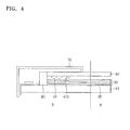
- FIG. 4 is a cross-sectional view of a display device according to another embodiment.
- the same reference numerals in FIGS. 1-3 and FIG. 4 denote the same elements and repeated descriptions thereof are omitted.
- an adhesion layer 41 that reflects light may be further formed between the thin film encapsulation 30 and the encapsulation substrate 50.
- the adhesion layer 41 may include metal particles 410.
- the metal particles 410 may be metal, such as Al or Ag having high reflectance. As the adhesion layer 41 includes the metal particles 410 having high reflectance, light loss may be reduced.
- the metal particles 410 included in the adhesion layer 41 may prevent light from passing therethrough.
- the metal particles 410 such as Al or Ag having high reflectance
- the metal particles 410 such as Al or Ag having high reflectance
- emission of light to the environment via the transparent adhesion layer 41 for example, light loss, may be prevented.
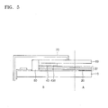
- FIG. 5 is a cross-sectional view of a display device according to another embodiment.
- the same reference numerals in FIGS. 1-3 and FIG. 5 denote the same elements and repeated descriptions thereof are omitted.
- an adhesion layer 43 may be further formed between the thin film encapsulation 30 and the encapsulation substrate 50, and a reflection layer 430 may be formed on an upper surface of the adhesion layer 43.
- the reflection layer 430 may be in the form of a thin film formed on the upper surface of the adhesion layer 43 and my reflect light that travels toward the adhesion layer 43.
- the reflection layer 430 may be formed on the upper surface of the adhesion layer 43.
- FIGS. 4 and 5 illustrate the adhesion layers 41 and 43 that are capable of reflecting light incident thereon in order to prevent light loss.
- any adhesion layer may be included as long as the adhesion layer is formed of a material capable of reflecting light or has a structure capable of reflecting light.
- a cover 70 may be included in the outer region B to surround the display device according to the present embodiment.
- the cover 70 corresponds to a frame of a TV, a bezel of a mobile phone, or the like.
- the cover 70 may be formed to surround the display device in order to prevent users from seeing internal wiring, circuits, and other unnecessary structures.
- a display device comprising: a substrate; a display unit formed over the substrate and configured to output light; a thin film encapsulation layer covering a portion of the display unit; and a photosensor formed adjacent an end of the thin film encapsulation layer.
- the thin film encapsulation layer is arranged to direct light from the display unit towards the photosensor.
- the photosensor is arranged to contact a lateral surface of the thin film encapsulation layer.
- the substrate comprises a light emitting region and an outer region, wherein the display unit is formed in the light emitting region and the photosensor is formed in the outer region of the substrate.
- the display device further comprises an encapsulation substrate formed over the thin film encapsulation layer and encapsulating the display unit.
- the thickness of the photosensor may be greater than the combined thickness of the thin film encapsulation layer and the encapsulation substrate.
- a top-emission type display device in a top-emission type display device, light loss is prevented, and a sufficient amount of light is transmitted to a photosensor.
Landscapes
- Chemical & Material Sciences (AREA)
- Inorganic Chemistry (AREA)
- Physics & Mathematics (AREA)
- Engineering & Computer Science (AREA)
- Microelectronics & Electronic Packaging (AREA)
- Optics & Photonics (AREA)
- Life Sciences & Earth Sciences (AREA)
- Sustainable Development (AREA)
- Geometry (AREA)
- Devices For Indicating Variable Information By Combining Individual Elements (AREA)
- Electroluminescent Light Sources (AREA)
Applications Claiming Priority (1)
| Application Number | Priority Date | Filing Date | Title |
|---|---|---|---|
| KR1020140184962A KR102246296B1 (ko) | 2014-12-19 | 2014-12-19 | 표시 장치 |
Publications (3)
| Publication Number | Publication Date |
|---|---|
| EP3035407A2 true EP3035407A2 (de) | 2016-06-22 |
| EP3035407A3 EP3035407A3 (de) | 2016-06-29 |
| EP3035407B1 EP3035407B1 (de) | 2019-11-13 |
Family
ID=55070700
Family Applications (1)
| Application Number | Title | Priority Date | Filing Date |
|---|---|---|---|
| EP15200430.5A Active EP3035407B1 (de) | 2014-12-19 | 2015-12-16 | Anzeigevorrichtung |
Country Status (4)
| Country | Link |
|---|---|
| US (1) | US9728594B2 (de) |
| EP (1) | EP3035407B1 (de) |
| KR (1) | KR102246296B1 (de) |
| CN (1) | CN105720078B (de) |
Families Citing this family (5)
| Publication number | Priority date | Publication date | Assignee | Title |
|---|---|---|---|---|
| TWI613804B (zh) * | 2017-09-04 | 2018-02-01 | 友達光電股份有限公司 | 光感測裝置 |
| KR102560100B1 (ko) * | 2018-03-08 | 2023-07-26 | 삼성디스플레이 주식회사 | 표시 장치 및 이의 제조 방법 |
| CN109950295B (zh) * | 2019-04-10 | 2021-03-23 | 合肥鑫晟光电科技有限公司 | Oled显示基板、oled显示装置、亮度补偿方法 |
| KR102811194B1 (ko) | 2020-04-21 | 2025-05-22 | 삼성전자주식회사 | 광학 센서를 포함하는 전자 장치 |
| CN114203750A (zh) * | 2021-12-07 | 2022-03-18 | 深圳市华星光电半导体显示技术有限公司 | 显示面板及其制备方法 |
Family Cites Families (27)
| Publication number | Priority date | Publication date | Assignee | Title |
|---|---|---|---|---|
| US6835950B2 (en) | 2002-04-12 | 2004-12-28 | Universal Display Corporation | Organic electronic devices with pressure sensitive adhesive layer |
| US7385572B2 (en) | 2002-09-09 | 2008-06-10 | E.I Du Pont De Nemours And Company | Organic electronic device having improved homogeneity |
| US7133032B2 (en) * | 2003-04-24 | 2006-11-07 | Eastman Kodak Company | OLED display and touch screen |
| JP4590283B2 (ja) * | 2004-05-21 | 2010-12-01 | シャープ株式会社 | バックライトユニット及びそれを備えた液晶表示装置 |
| BRPI0718194A2 (pt) * | 2006-10-05 | 2013-11-05 | Koninklijke Philips Electronics N.V. | Embalagem de módulo de luz |
| CN101763822B (zh) * | 2006-12-26 | 2012-10-03 | 乐金显示有限公司 | 有机发光二极管板 |
| KR100873082B1 (ko) * | 2007-05-30 | 2008-12-09 | 삼성모바일디스플레이주식회사 | 유기전계발광 표시 장치 및 그의 제조 방법 |
| KR101493092B1 (ko) | 2008-08-13 | 2015-02-23 | 엘지디스플레이 주식회사 | 유기전계발광표시소자 |
| KR20100024710A (ko) | 2008-08-26 | 2010-03-08 | 삼성모바일디스플레이주식회사 | 유기 발광 표시 장치 |
| KR100959105B1 (ko) * | 2008-10-15 | 2010-05-25 | 삼성모바일디스플레이주식회사 | 유기 발광 표시 장치 |
| US8957874B2 (en) * | 2009-06-29 | 2015-02-17 | Apple Inc. | Touch sensor panel design |
| US9000442B2 (en) * | 2010-01-20 | 2015-04-07 | Semiconductor Energy Laboratory Co., Ltd. | Light-emitting device, flexible light-emitting device, electronic device, and method for manufacturing light-emitting device and flexible-light emitting device |
| TWI422908B (zh) * | 2010-10-12 | 2014-01-11 | Au Optronics Corp | 觸控顯示裝置 |
| KR101430173B1 (ko) * | 2010-10-19 | 2014-08-13 | 삼성디스플레이 주식회사 | 유기 발광 표시 장치 |
| JP2012182053A (ja) | 2011-03-02 | 2012-09-20 | Sumitomo Chemical Co Ltd | バックライト装置 |
| CN103649883B (zh) * | 2011-07-11 | 2017-09-08 | 富士胶片株式会社 | 导电片及其制造方法、触摸屏以及显示装置 |
| KR101747735B1 (ko) | 2011-07-15 | 2017-06-16 | 엘지디스플레이 주식회사 | 표시 장치 및 그의 제조 방법 |
| KR101872963B1 (ko) | 2012-04-17 | 2018-06-29 | 엘지디스플레이 주식회사 | 유기발광 디스플레이 장치의 제조방법 |
| JP2014006759A (ja) * | 2012-06-26 | 2014-01-16 | Sony Corp | 情報処理装置および方法、並びに、光電変換装置 |
| KR101962851B1 (ko) * | 2012-07-19 | 2019-03-28 | 삼성디스플레이 주식회사 | 플렉서블 유기 발광 표시 장치 및 그 제조 방법 |
| KR101973168B1 (ko) * | 2012-08-24 | 2019-04-29 | 삼성디스플레이 주식회사 | 멀티 터치 및 터치 힘을 인식하는 터치 표시장치 및 그 구동 방법 |
| JP6092568B2 (ja) * | 2012-10-11 | 2017-03-08 | キヤノン株式会社 | 放射線検出装置及び放射線検出システム |
| US9070648B2 (en) * | 2012-11-27 | 2015-06-30 | Apple Inc. | Electronic devices with display-integrated light sensors |
| CN103107172B (zh) * | 2013-01-15 | 2015-10-21 | 深圳典邦科技有限公司 | 微显示集成背照图像传感器的oled图像收发装置 |
| JP6468686B2 (ja) * | 2014-04-25 | 2019-02-13 | 株式会社半導体エネルギー研究所 | 入出力装置 |
| KR20160038150A (ko) * | 2014-09-29 | 2016-04-07 | 삼성디스플레이 주식회사 | 표시장치 |
| JP2016111211A (ja) * | 2014-12-08 | 2016-06-20 | セイコーエプソン株式会社 | 光電変換装置および電子機器 |
-
2014
- 2014-12-19 KR KR1020140184962A patent/KR102246296B1/ko active Active
-
2015
- 2015-08-27 US US14/838,224 patent/US9728594B2/en active Active
- 2015-12-10 CN CN201510908847.4A patent/CN105720078B/zh active Active
- 2015-12-16 EP EP15200430.5A patent/EP3035407B1/de active Active
Non-Patent Citations (1)
| Title |
|---|
| None |
Also Published As
| Publication number | Publication date |
|---|---|
| US20160181342A1 (en) | 2016-06-23 |
| US9728594B2 (en) | 2017-08-08 |
| CN105720078A (zh) | 2016-06-29 |
| EP3035407B1 (de) | 2019-11-13 |
| KR102246296B1 (ko) | 2021-04-30 |
| EP3035407A3 (de) | 2016-06-29 |
| KR20160076011A (ko) | 2016-06-30 |
| CN105720078B (zh) | 2021-02-02 |
Similar Documents
| Publication | Publication Date | Title |
|---|---|---|
| US11411202B2 (en) | Display device | |
| US8981362B2 (en) | Organic light-emitting display device and method of manufacturing the same | |
| EP2811522B1 (de) | Organische lichtemittierende Anzeigevorrichtung | |
| US10944071B2 (en) | Organic light-emitting display apparatus and method of manufacturing the same | |
| US9252388B2 (en) | Organic light emitting diode (OLED) display | |
| EP2608288B1 (de) | Organische lichtemittierende Anzeigevorrichtung und Herstellungsverfahren dafür | |
| US9859346B2 (en) | Organic light-emitting diode display and method of manufacturing the same | |
| US8895972B2 (en) | Display device and organic light emitting display device having auxiliary electrode | |
| EP3035407B1 (de) | Anzeigevorrichtung | |
| US10211425B2 (en) | Display device and method of manufacturing the same |
Legal Events
| Date | Code | Title | Description |
|---|---|---|---|
| PUAI | Public reference made under article 153(3) epc to a published international application that has entered the european phase |
Free format text: ORIGINAL CODE: 0009012 |
|
| PUAL | Search report despatched |
Free format text: ORIGINAL CODE: 0009013 |
|
| AK | Designated contracting states |
Kind code of ref document: A2 Designated state(s): AL AT BE BG CH CY CZ DE DK EE ES FI FR GB GR HR HU IE IS IT LI LT LU LV MC MK MT NL NO PL PT RO RS SE SI SK SM TR |
|
| AX | Request for extension of the european patent |
Extension state: BA ME |
|
| AK | Designated contracting states |
Kind code of ref document: A3 Designated state(s): AL AT BE BG CH CY CZ DE DK EE ES FI FR GB GR HR HU IE IS IT LI LT LU LV MC MK MT NL NO PL PT RO RS SE SI SK SM TR |
|
| AX | Request for extension of the european patent |
Extension state: BA ME |
|
| RIC1 | Information provided on ipc code assigned before grant |
Ipc: H01L 27/32 20060101ALI20160523BHEP Ipc: H01L 51/52 20060101AFI20160523BHEP |
|
| STAA | Information on the status of an ep patent application or granted ep patent |
Free format text: STATUS: REQUEST FOR EXAMINATION WAS MADE |
|
| 17P | Request for examination filed |
Effective date: 20161229 |
|
| RBV | Designated contracting states (corrected) |
Designated state(s): AL AT BE BG CH CY CZ DE DK EE ES FI FR GB GR HR HU IE IS IT LI LT LU LV MC MK MT NL NO PL PT RO RS SE SI SK SM TR |
|
| STAA | Information on the status of an ep patent application or granted ep patent |
Free format text: STATUS: EXAMINATION IS IN PROGRESS |
|
| 17Q | First examination report despatched |
Effective date: 20180920 |
|
| GRAP | Despatch of communication of intention to grant a patent |
Free format text: ORIGINAL CODE: EPIDOSNIGR1 |
|
| STAA | Information on the status of an ep patent application or granted ep patent |
Free format text: STATUS: GRANT OF PATENT IS INTENDED |
|
| INTG | Intention to grant announced |
Effective date: 20190521 |
|
| GRAS | Grant fee paid |
Free format text: ORIGINAL CODE: EPIDOSNIGR3 |
|
| GRAA | (expected) grant |
Free format text: ORIGINAL CODE: 0009210 |
|
| STAA | Information on the status of an ep patent application or granted ep patent |
Free format text: STATUS: THE PATENT HAS BEEN GRANTED |
|
| AK | Designated contracting states |
Kind code of ref document: B1 Designated state(s): AL AT BE BG CH CY CZ DE DK EE ES FI FR GB GR HR HU IE IS IT LI LT LU LV MC MK MT NL NO PL PT RO RS SE SI SK SM TR |
|
| REG | Reference to a national code |
Ref country code: CH Ref legal event code: EP Ref country code: AT Ref legal event code: REF Ref document number: 1202595 Country of ref document: AT Kind code of ref document: T Effective date: 20191115 |
|
| REG | Reference to a national code |
Ref country code: DE Ref legal event code: R096 Ref document number: 602015041548 Country of ref document: DE |
|
| REG | Reference to a national code |
Ref country code: IE Ref legal event code: FG4D |
|
| REG | Reference to a national code |
Ref country code: NL Ref legal event code: MP Effective date: 20191113 |
|
| REG | Reference to a national code |
Ref country code: LT Ref legal event code: MG4D |
|
| PG25 | Lapsed in a contracting state [announced via postgrant information from national office to epo] |
Ref country code: PL Free format text: LAPSE BECAUSE OF FAILURE TO SUBMIT A TRANSLATION OF THE DESCRIPTION OR TO PAY THE FEE WITHIN THE PRESCRIBED TIME-LIMIT Effective date: 20191113 Ref country code: NL Free format text: LAPSE BECAUSE OF FAILURE TO SUBMIT A TRANSLATION OF THE DESCRIPTION OR TO PAY THE FEE WITHIN THE PRESCRIBED TIME-LIMIT Effective date: 20191113 Ref country code: FI Free format text: LAPSE BECAUSE OF FAILURE TO SUBMIT A TRANSLATION OF THE DESCRIPTION OR TO PAY THE FEE WITHIN THE PRESCRIBED TIME-LIMIT Effective date: 20191113 Ref country code: LT Free format text: LAPSE BECAUSE OF FAILURE TO SUBMIT A TRANSLATION OF THE DESCRIPTION OR TO PAY THE FEE WITHIN THE PRESCRIBED TIME-LIMIT Effective date: 20191113 Ref country code: BG Free format text: LAPSE BECAUSE OF FAILURE TO SUBMIT A TRANSLATION OF THE DESCRIPTION OR TO PAY THE FEE WITHIN THE PRESCRIBED TIME-LIMIT Effective date: 20200213 Ref country code: LV Free format text: LAPSE BECAUSE OF FAILURE TO SUBMIT A TRANSLATION OF THE DESCRIPTION OR TO PAY THE FEE WITHIN THE PRESCRIBED TIME-LIMIT Effective date: 20191113 Ref country code: SE Free format text: LAPSE BECAUSE OF FAILURE TO SUBMIT A TRANSLATION OF THE DESCRIPTION OR TO PAY THE FEE WITHIN THE PRESCRIBED TIME-LIMIT Effective date: 20191113 Ref country code: NO Free format text: LAPSE BECAUSE OF FAILURE TO SUBMIT A TRANSLATION OF THE DESCRIPTION OR TO PAY THE FEE WITHIN THE PRESCRIBED TIME-LIMIT Effective date: 20200213 Ref country code: GR Free format text: LAPSE BECAUSE OF FAILURE TO SUBMIT A TRANSLATION OF THE DESCRIPTION OR TO PAY THE FEE WITHIN THE PRESCRIBED TIME-LIMIT Effective date: 20200214 Ref country code: PT Free format text: LAPSE BECAUSE OF FAILURE TO SUBMIT A TRANSLATION OF THE DESCRIPTION OR TO PAY THE FEE WITHIN THE PRESCRIBED TIME-LIMIT Effective date: 20200313 |
|
| PG25 | Lapsed in a contracting state [announced via postgrant information from national office to epo] |
Ref country code: RS Free format text: LAPSE BECAUSE OF FAILURE TO SUBMIT A TRANSLATION OF THE DESCRIPTION OR TO PAY THE FEE WITHIN THE PRESCRIBED TIME-LIMIT Effective date: 20191113 Ref country code: HR Free format text: LAPSE BECAUSE OF FAILURE TO SUBMIT A TRANSLATION OF THE DESCRIPTION OR TO PAY THE FEE WITHIN THE PRESCRIBED TIME-LIMIT Effective date: 20191113 Ref country code: IS Free format text: LAPSE BECAUSE OF FAILURE TO SUBMIT A TRANSLATION OF THE DESCRIPTION OR TO PAY THE FEE WITHIN THE PRESCRIBED TIME-LIMIT Effective date: 20200313 |
|
| PG25 | Lapsed in a contracting state [announced via postgrant information from national office to epo] |
Ref country code: AL Free format text: LAPSE BECAUSE OF FAILURE TO SUBMIT A TRANSLATION OF THE DESCRIPTION OR TO PAY THE FEE WITHIN THE PRESCRIBED TIME-LIMIT Effective date: 20191113 |
|
| PG25 | Lapsed in a contracting state [announced via postgrant information from national office to epo] |
Ref country code: CZ Free format text: LAPSE BECAUSE OF FAILURE TO SUBMIT A TRANSLATION OF THE DESCRIPTION OR TO PAY THE FEE WITHIN THE PRESCRIBED TIME-LIMIT Effective date: 20191113 Ref country code: RO Free format text: LAPSE BECAUSE OF FAILURE TO SUBMIT A TRANSLATION OF THE DESCRIPTION OR TO PAY THE FEE WITHIN THE PRESCRIBED TIME-LIMIT Effective date: 20191113 Ref country code: DK Free format text: LAPSE BECAUSE OF FAILURE TO SUBMIT A TRANSLATION OF THE DESCRIPTION OR TO PAY THE FEE WITHIN THE PRESCRIBED TIME-LIMIT Effective date: 20191113 Ref country code: EE Free format text: LAPSE BECAUSE OF FAILURE TO SUBMIT A TRANSLATION OF THE DESCRIPTION OR TO PAY THE FEE WITHIN THE PRESCRIBED TIME-LIMIT Effective date: 20191113 Ref country code: ES Free format text: LAPSE BECAUSE OF FAILURE TO SUBMIT A TRANSLATION OF THE DESCRIPTION OR TO PAY THE FEE WITHIN THE PRESCRIBED TIME-LIMIT Effective date: 20191113 |
|
| REG | Reference to a national code |
Ref country code: CH Ref legal event code: PL |
|
| REG | Reference to a national code |
Ref country code: DE Ref legal event code: R097 Ref document number: 602015041548 Country of ref document: DE |
|
| REG | Reference to a national code |
Ref country code: AT Ref legal event code: MK05 Ref document number: 1202595 Country of ref document: AT Kind code of ref document: T Effective date: 20191113 |
|
| REG | Reference to a national code |
Ref country code: BE Ref legal event code: MM Effective date: 20191231 |
|
| PG25 | Lapsed in a contracting state [announced via postgrant information from national office to epo] |
Ref country code: SK Free format text: LAPSE BECAUSE OF FAILURE TO SUBMIT A TRANSLATION OF THE DESCRIPTION OR TO PAY THE FEE WITHIN THE PRESCRIBED TIME-LIMIT Effective date: 20191113 Ref country code: SM Free format text: LAPSE BECAUSE OF FAILURE TO SUBMIT A TRANSLATION OF THE DESCRIPTION OR TO PAY THE FEE WITHIN THE PRESCRIBED TIME-LIMIT Effective date: 20191113 Ref country code: MC Free format text: LAPSE BECAUSE OF FAILURE TO SUBMIT A TRANSLATION OF THE DESCRIPTION OR TO PAY THE FEE WITHIN THE PRESCRIBED TIME-LIMIT Effective date: 20191113 |
|
| PLBE | No opposition filed within time limit |
Free format text: ORIGINAL CODE: 0009261 |
|
| STAA | Information on the status of an ep patent application or granted ep patent |
Free format text: STATUS: NO OPPOSITION FILED WITHIN TIME LIMIT |
|
| 26N | No opposition filed |
Effective date: 20200814 |
|
| PG25 | Lapsed in a contracting state [announced via postgrant information from national office to epo] |
Ref country code: LU Free format text: LAPSE BECAUSE OF NON-PAYMENT OF DUE FEES Effective date: 20191216 Ref country code: IE Free format text: LAPSE BECAUSE OF NON-PAYMENT OF DUE FEES Effective date: 20191216 |
|
| PG25 | Lapsed in a contracting state [announced via postgrant information from national office to epo] |
Ref country code: LI Free format text: LAPSE BECAUSE OF NON-PAYMENT OF DUE FEES Effective date: 20191231 Ref country code: CH Free format text: LAPSE BECAUSE OF NON-PAYMENT OF DUE FEES Effective date: 20191231 Ref country code: AT Free format text: LAPSE BECAUSE OF FAILURE TO SUBMIT A TRANSLATION OF THE DESCRIPTION OR TO PAY THE FEE WITHIN THE PRESCRIBED TIME-LIMIT Effective date: 20191113 Ref country code: BE Free format text: LAPSE BECAUSE OF NON-PAYMENT OF DUE FEES Effective date: 20191231 Ref country code: SI Free format text: LAPSE BECAUSE OF FAILURE TO SUBMIT A TRANSLATION OF THE DESCRIPTION OR TO PAY THE FEE WITHIN THE PRESCRIBED TIME-LIMIT Effective date: 20191113 |
|
| PG25 | Lapsed in a contracting state [announced via postgrant information from national office to epo] |
Ref country code: IT Free format text: LAPSE BECAUSE OF FAILURE TO SUBMIT A TRANSLATION OF THE DESCRIPTION OR TO PAY THE FEE WITHIN THE PRESCRIBED TIME-LIMIT Effective date: 20191113 |
|
| PG25 | Lapsed in a contracting state [announced via postgrant information from national office to epo] |
Ref country code: CY Free format text: LAPSE BECAUSE OF FAILURE TO SUBMIT A TRANSLATION OF THE DESCRIPTION OR TO PAY THE FEE WITHIN THE PRESCRIBED TIME-LIMIT Effective date: 20191113 |
|
| PG25 | Lapsed in a contracting state [announced via postgrant information from national office to epo] |
Ref country code: HU Free format text: LAPSE BECAUSE OF FAILURE TO SUBMIT A TRANSLATION OF THE DESCRIPTION OR TO PAY THE FEE WITHIN THE PRESCRIBED TIME-LIMIT; INVALID AB INITIO Effective date: 20151216 Ref country code: MT Free format text: LAPSE BECAUSE OF FAILURE TO SUBMIT A TRANSLATION OF THE DESCRIPTION OR TO PAY THE FEE WITHIN THE PRESCRIBED TIME-LIMIT Effective date: 20191113 |
|
| PG25 | Lapsed in a contracting state [announced via postgrant information from national office to epo] |
Ref country code: TR Free format text: LAPSE BECAUSE OF FAILURE TO SUBMIT A TRANSLATION OF THE DESCRIPTION OR TO PAY THE FEE WITHIN THE PRESCRIBED TIME-LIMIT Effective date: 20191113 |
|
| PG25 | Lapsed in a contracting state [announced via postgrant information from national office to epo] |
Ref country code: MK Free format text: LAPSE BECAUSE OF FAILURE TO SUBMIT A TRANSLATION OF THE DESCRIPTION OR TO PAY THE FEE WITHIN THE PRESCRIBED TIME-LIMIT Effective date: 20191113 |
|
| REG | Reference to a national code |
Ref country code: DE Ref legal event code: R079 Ref document number: 602015041548 Country of ref document: DE Free format text: PREVIOUS MAIN CLASS: H01L0051520000 Ipc: H10K0050800000 |
|
| P01 | Opt-out of the competence of the unified patent court (upc) registered |
Effective date: 20230515 |
|
| PGFP | Annual fee paid to national office [announced via postgrant information from national office to epo] |
Ref country code: DE Payment date: 20251120 Year of fee payment: 11 |
|
| PGFP | Annual fee paid to national office [announced via postgrant information from national office to epo] |
Ref country code: GB Payment date: 20251120 Year of fee payment: 11 |
|
| PGFP | Annual fee paid to national office [announced via postgrant information from national office to epo] |
Ref country code: FR Payment date: 20251125 Year of fee payment: 11 |