EP3026695A1 - Method for manufacturing injection-enhanced insulated-gate bipolar transistor - Google Patents
Method for manufacturing injection-enhanced insulated-gate bipolar transistor Download PDFInfo
- Publication number
- EP3026695A1 EP3026695A1 EP14829488.7A EP14829488A EP3026695A1 EP 3026695 A1 EP3026695 A1 EP 3026695A1 EP 14829488 A EP14829488 A EP 14829488A EP 3026695 A1 EP3026695 A1 EP 3026695A1
- Authority
- EP
- European Patent Office
- Prior art keywords
- layer
- type
- trench
- type doped
- doped layer
- Prior art date
- Legal status (The legal status is an assumption and is not a legal conclusion. Google has not performed a legal analysis and makes no representation as to the accuracy of the status listed.)
- Granted
Links
Images




Classifications
-
- H—ELECTRICITY
- H10—SEMICONDUCTOR DEVICES; ELECTRIC SOLID-STATE DEVICES NOT OTHERWISE PROVIDED FOR
- H10D—INORGANIC ELECTRIC SEMICONDUCTOR DEVICES
- H10D12/00—Bipolar devices controlled by the field effect, e.g. insulated-gate bipolar transistors [IGBT]
- H10D12/01—Manufacture or treatment
- H10D12/031—Manufacture or treatment of IGBTs
- H10D12/032—Manufacture or treatment of IGBTs of vertical IGBTs
- H10D12/038—Manufacture or treatment of IGBTs of vertical IGBTs having a recessed gate, e.g. trench-gate IGBTs
-
- H—ELECTRICITY
- H10—SEMICONDUCTOR DEVICES; ELECTRIC SOLID-STATE DEVICES NOT OTHERWISE PROVIDED FOR
- H10D—INORGANIC ELECTRIC SEMICONDUCTOR DEVICES
- H10D12/00—Bipolar devices controlled by the field effect, e.g. insulated-gate bipolar transistors [IGBT]
- H10D12/411—Insulated-gate bipolar transistors [IGBT]
- H10D12/441—Vertical IGBTs
- H10D12/461—Vertical IGBTs having non-planar surfaces, e.g. having trenches, recesses or pillars in the surfaces of the emitter, base or collector regions
- H10D12/481—Vertical IGBTs having non-planar surfaces, e.g. having trenches, recesses or pillars in the surfaces of the emitter, base or collector regions having gate structures on slanted surfaces, on vertical surfaces, or in grooves, e.g. trench gate IGBTs
-
- H—ELECTRICITY
- H10—SEMICONDUCTOR DEVICES; ELECTRIC SOLID-STATE DEVICES NOT OTHERWISE PROVIDED FOR
- H10D—INORGANIC ELECTRIC SEMICONDUCTOR DEVICES
- H10D62/00—Semiconductor bodies, or regions thereof, of devices having potential barriers
- H10D62/10—Shapes, relative sizes or dispositions of the regions of the semiconductor bodies; Shapes of the semiconductor bodies
- H10D62/102—Constructional design considerations for preventing surface leakage or controlling electric field concentration
- H10D62/103—Constructional design considerations for preventing surface leakage or controlling electric field concentration for increasing or controlling the breakdown voltage of reverse-biased devices
- H10D62/105—Constructional design considerations for preventing surface leakage or controlling electric field concentration for increasing or controlling the breakdown voltage of reverse-biased devices by having particular doping profiles, shapes or arrangements of PN junctions; by having supplementary regions, e.g. junction termination extension [JTE]
- H10D62/109—Reduced surface field [RESURF] PN junction structures
-
- H—ELECTRICITY
- H10—SEMICONDUCTOR DEVICES; ELECTRIC SOLID-STATE DEVICES NOT OTHERWISE PROVIDED FOR
- H10D—INORGANIC ELECTRIC SEMICONDUCTOR DEVICES
- H10D62/00—Semiconductor bodies, or regions thereof, of devices having potential barriers
- H10D62/10—Shapes, relative sizes or dispositions of the regions of the semiconductor bodies; Shapes of the semiconductor bodies
- H10D62/17—Semiconductor regions connected to electrodes not carrying current to be rectified, amplified or switched, e.g. channel regions
- H10D62/393—Body regions of DMOS transistors or IGBTs
-
- H—ELECTRICITY
- H10—SEMICONDUCTOR DEVICES; ELECTRIC SOLID-STATE DEVICES NOT OTHERWISE PROVIDED FOR
- H10P—GENERIC PROCESSES OR APPARATUS FOR THE MANUFACTURE OR TREATMENT OF DEVICES COVERED BY CLASS H10
- H10P30/00—Ion implantation into wafers, substrates or parts of devices
- H10P30/20—Ion implantation into wafers, substrates or parts of devices into semiconductor materials, e.g. for doping
- H10P30/202—Ion implantation into wafers, substrates or parts of devices into semiconductor materials, e.g. for doping characterised by the semiconductor materials
- H10P30/204—Ion implantation into wafers, substrates or parts of devices into semiconductor materials, e.g. for doping characterised by the semiconductor materials into Group IV semiconductors
-
- H—ELECTRICITY
- H10—SEMICONDUCTOR DEVICES; ELECTRIC SOLID-STATE DEVICES NOT OTHERWISE PROVIDED FOR
- H10P—GENERIC PROCESSES OR APPARATUS FOR THE MANUFACTURE OR TREATMENT OF DEVICES COVERED BY CLASS H10
- H10P30/00—Ion implantation into wafers, substrates or parts of devices
- H10P30/20—Ion implantation into wafers, substrates or parts of devices into semiconductor materials, e.g. for doping
- H10P30/21—Ion implantation into wafers, substrates or parts of devices into semiconductor materials, e.g. for doping of electrically active species
-
- H—ELECTRICITY
- H10—SEMICONDUCTOR DEVICES; ELECTRIC SOLID-STATE DEVICES NOT OTHERWISE PROVIDED FOR
- H10P—GENERIC PROCESSES OR APPARATUS FOR THE MANUFACTURE OR TREATMENT OF DEVICES COVERED BY CLASS H10
- H10P30/00—Ion implantation into wafers, substrates or parts of devices
- H10P30/20—Ion implantation into wafers, substrates or parts of devices into semiconductor materials, e.g. for doping
- H10P30/22—Ion implantation into wafers, substrates or parts of devices into semiconductor materials, e.g. for doping using masks
-
- H—ELECTRICITY
- H10—SEMICONDUCTOR DEVICES; ELECTRIC SOLID-STATE DEVICES NOT OTHERWISE PROVIDED FOR
- H10P—GENERIC PROCESSES OR APPARATUS FOR THE MANUFACTURE OR TREATMENT OF DEVICES COVERED BY CLASS H10
- H10P32/00—Diffusion of dopants within, into or out of wafers, substrates or parts of devices
- H10P32/10—Diffusion of dopants within, into or out of semiconductor bodies or layers
- H10P32/14—Diffusion of dopants within, into or out of semiconductor bodies or layers within a single semiconductor body or layer in a solid phase; between different semiconductor bodies or layers, both in a solid phase
- H10P32/1404—Diffusion of dopants within, into or out of semiconductor bodies or layers within a single semiconductor body or layer in a solid phase; between different semiconductor bodies or layers, both in a solid phase using predeposition followed by drive-in of impurities into the semiconductor surface, e.g. predeposition from a gaseous phase
- H10P32/1406—Diffusion of dopants within, into or out of semiconductor bodies or layers within a single semiconductor body or layer in a solid phase; between different semiconductor bodies or layers, both in a solid phase using predeposition followed by drive-in of impurities into the semiconductor surface, e.g. predeposition from a gaseous phase by ion implantation
-
- H—ELECTRICITY
- H10—SEMICONDUCTOR DEVICES; ELECTRIC SOLID-STATE DEVICES NOT OTHERWISE PROVIDED FOR
- H10P—GENERIC PROCESSES OR APPARATUS FOR THE MANUFACTURE OR TREATMENT OF DEVICES COVERED BY CLASS H10
- H10P32/00—Diffusion of dopants within, into or out of wafers, substrates or parts of devices
- H10P32/10—Diffusion of dopants within, into or out of semiconductor bodies or layers
- H10P32/17—Diffusion of dopants within, into or out of semiconductor bodies or layers characterised by the semiconductor material
- H10P32/171—Diffusion of dopants within, into or out of semiconductor bodies or layers characterised by the semiconductor material being group IV material
-
- H—ELECTRICITY
- H10—SEMICONDUCTOR DEVICES; ELECTRIC SOLID-STATE DEVICES NOT OTHERWISE PROVIDED FOR
- H10P—GENERIC PROCESSES OR APPARATUS FOR THE MANUFACTURE OR TREATMENT OF DEVICES COVERED BY CLASS H10
- H10P95/00—Generic processes or apparatus for manufacture or treatments not covered by the other groups of this subclass
- H10P95/90—Thermal treatments, e.g. annealing or sintering
Definitions
- the present invention relates to a technical field of semiconductor manufacture, and more particularly, relates to a method of manufacturing an injection-enhanced Insulated Gate Bipolar Transistor.
- the buffer layer is formed by generally implanting an N-type dopant, and then a drive-in is performed, a body implantation is performed, then a drive-in is performed again, such that a time period of the drive-in for forming the buffer layer is longer than a time period of the drive-in for forming the body, which results in that a junction depth of the N-type dopant to be deeper than a junction depth of the body.
- IGBT injection-enhanced insulated gate bipolar transistor
- the N-type dopant is distributed and diffused by virtue of a long time period of drive-in, causing the junction depth of the N-type dopant to be deeper than the junction depth of the body, an N+ is formed beneath the body, such that an enhanced injection can be achieved.
- the method of manufacturing the injection-enhanced IGBT requires additionally adding a drive-in process, the production cycle thereof is long.
- a method of manufacturing an injection-enhanced IGBT includes steps as follow: providing an N-type substrate; forming a P-type doped layer on the N-type substrate; forming a hard layer on the P-type doped layer; etching the hard layer to form a hard layer having a trench pattern; etching the P-type doped layer to form a trench extending into the N-type substrate; forming an N-type doped layer on a sidewall and a bottom of the trench; removing the hard layer having the trench pattern; performing a drive-in to the P-type dopant of the P-type doped layer and the N-type dopant of the N-type doped layer together, the P-type dopant forms a P-type base region by diffusing, and the N-type dopant forms an N-type buffer layer by diffusing; forming a gate oxide dielectric layer on a surface of the trench; and depositing a polysilicon layer in the trench on which the gate oxide dielectric layer is formed.
- the P-type doped layer is formed by ion implantation or diffusion.
- a concentration of P-type dopant in the P-type doped layer is from 1 ⁇ 10 12 /cm 3 to 1 ⁇ 10 20 /cm 3 .
- the hard layer is adopted as a mask
- the N-type doped layer is formed by diffusion technology.
- a concentration of N-type dopant in the N-type doped layer is from 1 ⁇ 10 12 /cm 3 to 1 ⁇ 10 20 /cm 3 .
- a temperature of the drive-in is from 1100°C to 1280°C.
- a time period of the drive-in is from 20 min to500 min.
- the forming the gate oxide dielectric layer on the surface of the trench comprises: oxidizing the surface of the trench to form a sacrificial oxide layer; removing the sacrificial oxide layer by etching; oxidizing the surface of the trench to form the gate oxide dielectric layer.
- the hard layer is made of silicon oxide or silicon nitride.
- a method of manufacturing an injection-enhanced IGBT includes steps as follow: providing an N-type substrate; forming a hard layer on the N-type doped layer; etching the hard layer to form a hard layer having a trench pattern; etching the N-type doped layer to form a trench; forming an N-type doped layer on a sidewall and a bottom of the trench; removing the hard layer having the trench pattern; forming a mask layer in the trench, the mask layer filling the trench; forming a P-type doped layer on a surface of the N-type substrate which forms the trench; removing the mask layer; performing a drive-in to the P-type dopant of the P-type doped layer and the N-type dopant of the N-type doped layer together, the P-type dopant forming a P-type base region by diffusing, and the N-type dopant forming an N-type buffer layer by diffusing; forming a gate oxide dielectric layer on a surface of the trench; and
- the P-type dopant of the P-type doped layer and the N-type dopant of the N-type doped layer are driven-in together to form a P-type base region and an N-type buffer layer, only one drive-in process is required, the production cycle is shortened in comparison with a conventional method of manufacturing injection-enhanced IGBT.
- a method of manufacturing an injection-enhanced IGBT includes the following steps:
- the specific resistance of the N-type substrate 12 is in a range of from about 0.01 ⁇ *cm to 200 ⁇ *cm.
- the N-type substrate 12 having different specific resistances can be selected according to the IGBT product.
- the N-type substrate 12 can have a thickness in a range of from 100 ⁇ m to 1000 ⁇ m.
- a P-type doped layer 14 is formed on the N-type substrate 12.
- a P-type doped layer 14 is formed by performing a P-type doping to the N-type substrate 12.
- the P-type doped layer 14 can be formed by diffusion or ion implantation.
- the forming method of the P-type doped layer 14 is not limited herein.
- the implanted ion can be boron (B), and an implantation concentration of the ions can be from 1 ⁇ 10 12 /cm 3 to 1 ⁇ 10 20 /cm 3 .
- the energy of the implantation ion can be from 20KeV to 200KeV
- a hard layer is formed on the P-type doped layer.
- the hard layer 20 can be made of silicon oxide or silicon nitride.
- the thickness of the hard layer 20 can be in a range of 500 angstrom to 100000 angstrom. In practical application, the thickness of the hard layer 20 can be other values.
- the hard layer 20 covers the P-type doped layer 14.
- the hard layer 20 can be formed by methods such as lower pressure SiO 2 vapor deposition technology, furnace oxidation, rapid thermal annealing oxidation or in-situ vapor oxidation.
- the hard layer 20 can be manufactured by chemical vapor deposition technology.
- a hard layer having a trench pattern is formed by etching the hard layer.
- the hard layer having the trench pattern is formed by adopting photolithography and etching method to etch the hard layer.
- a photoresist layer 30 is formed on the hard layer 20 first. And then, the photoresist layer 30 is placed beneath an exposure equipment, a photo-mask having the trench pattern on its surface is adopted to perform a photo-mask exposure, the trench pattern on the photo-mask is transferred to the photoresist layer 30, and then developing solution is adopted to remove the photoresist on the exposure region, the photoresist layer 30 having the trench pattern is formed. Referring to FIG. 5 , the photoresist layer 30 having the trench pattern is adopted as a mask, the hard layer 20 is etched to form the hard layer 20 having the trench pattern.
- the photoresist layer 30 can be formed by static drip or spin coating technology.
- a trench is formed by etching the P-type doped layer, and the trench extends into the N-type substrate.
- a depth of the trench 40 extends through the P-type doped layer 14, and the depth of the trench 40 is deeper than a thickness of the P-body 60 which is formed by performing a drive-in to the P-type doped layer 14.
- the depth of the trench 40 can be in a range of 0.5 ⁇ m to 15 ⁇ m. In practical application, one skilled in the art can select the depth of the trench 40 according to a specific condition.
- the photoresist layer 30 can be removed.
- the photoresist layer 30 can also be removed after forming trench 40 on the P-type doped layer 12.
- the photoresist layer 30 can be removed by dry stripping or wet stripping technology.
- the dry stripping technology adopts plasma to bombard the photoresist to remove the photoresist layer 30.
- the wet stripping technology adopts cleaning solution to remove the photoresist layer 30.
- the cleaning solution adopted by the wet stripping technology can be a mixed liquid of sulfuric acid and oxidizing agent. In other embodiments, the cleaning solution of the wet stripping technology can be other mixture material. It should be noted that, one skilled in the art can selectively adopt the dry stripping technology or the wet stripping technology to remove the photoresist layer 30 according to a practical situation.
- an N-type doped layer is formed on a sidewall and a bottom of the trench.
- the hard layer 20 having the trench pattern is adopted as a mask, and the N-type doped layer 50 is formed on the sidewall and the bottom of the trench 40 by a diffusion technology.
- the temperature of the diffusion technology is from 800°C to 1250°C
- the time period of the diffusion technology is from 10min to 300min
- the diffusion source is an N-type dopant, such as B 2 O 3 , POCl 3 or PH 3 .
- the diffusion source is POCl 3 .
- the concentration of the N-type dopant of the N-type doped layer 50 is from 1 ⁇ 10 12 /cm 3 to 1 ⁇ 10 20 /cm 3 .
- the category and concentration of dopant in the growth process can be controlled according to a specific requirement of the device.
- the N-type doped layer 50 has a thickness from 0.5 ⁇ m to 20 ⁇ m.
- the hard layer 20 having the trench pattern is removed.
- the hard layer 20 is an oxide
- the hard layer 20 covering on the P-type doped layer 14 is removed by the plasma etching technology or by the buffer oxide etching technology
- the structure after removing the hard layer 20 is shown as FIG. 8 .
- the buffer oxide etching technology can adopt a mixed solution of hydrofluoric acid (49%), water and ammonium fluoride to rinse the hard layer 20.
- a removal rate of the hard layer 20 can be adjusted by adjusting concentrations of the hydrofluoric acid and the ammonium fluoride.
- the hard layer 20 When the hard layer 20 is nitride, the hard layer 20 can be removed by wet etching.
- the P-type dopant of the P-type doped layer and the N-type dopant of the N-type doped layer are driven-in together, the P-type dopant forms a P-type base region by diffusing, and the N-type dopant forms an N-type buffer layer by diffusing.
- the drive-in allows the implanted N-type dopant and the P-type dopant to penetrate the silicon crystal in the N-type substrate 12 and form a desired junction depth in the N-type substrate 12, and form a P-type base region and an N-type buffer layer,.
- the temperature of drive-in can be from 1100°C to 1280°C
- the time period of drive-in can be from 20 min to 500 min. In practical application, the temperature and time period of the drive-in can be adjusted according to a specific requirement of the device.
- a gate oxide dielectric layer is formed on the surface of the trench.
- the operation for forming the gate oxide dielectric layer on the surface of the trench includes:
- the gate oxide dielectric layer 80 Because many more defects are inevitably formed on the surface of the trench 40 when etching the trench, it affects the quality of the gate oxide dielectric layer 80. Therefore, when the surface of the trench 40 is oxidized to form a sacrificial oxide layer first, and then the sacrificial oxide layer is etched to be removed, and then the gate oxide dielectric layer 80 is formed by oxidization, it facilitates to improve the oneness of the material and the homogeneity of the gate oxide dielectric layer 40, and improving the quality of the gate oxide dielectric layer.
- the sacrificial oxide layer can be formed by a dry oxidization or a wet oxidization.
- the sacrificial oxide layer can be removed by a wet etching.
- the gate oxide dielectric layer 80 can be formed by a dry oxidization.
- the oxidizing method of the gate oxide dielectric layer 80 is not limited.
- an appropriate oxidizing method of the gate oxide dielectric layer 80 can be selected according to a requirement of the quality of the gate oxide dielectric layer 80.
- a thickness of the gate oxide dielectric layer 80 can be in a range from 100 angstrom to 5000 angstrom, for example, the thickness is 1000 angstrom.
- a polysilicon layer is deposited in the trench on which the gate oxide dielectric layer is formed.
- the structure after depositing a polysilicon layer in the trench on which the gate oxide dielectric layer is formed and a back etching is shown as FIG. 11 .
- the polysilicon layer can be formed by chemical vapor deposition, physical vapor deposition or other ways. In practical application, an appropriate deposition method can be selected according to a requirement.
- the polysilicon layer 90 can adopt a dry etching to back etch the polysilicon layer, to remove the redundant deposition.
- a gate electrode is formed by performing subsequent processes to the polysilicon layer 90. Subsequently, an emitting electrode and a collector electrode are formed by performing front processes, backgrind, back implantation, annealing, and back metallization and other steps to the device obtained by S190, an injection-enhanced IGBT is obtained. All technologies such as performing subsequent processes to the polysilicon layer 9 to form a gate electrode, front processes, backgrind, back implantation, annealing, and back metallization can adopt customary means in the technical field, and will not be limited hereby.
- Above described method of manufacturing an injection-enhanced IGBT is merely directed to an operation including: forming a P-type doped layer on the surface of the N-type substrate first; performing an etching to the trench subsequently; and then forming an N-type doped layer by diffusion technology; and then performing a drive-in to the P-type dopant of the P-type doped layer and the N-type dopant of the N-type doped layer together.
- a method of manufacturing an injection-enhanced IGBT includes the following steps:
- the N-type substrate provided in S210 is same as the N-type substrate provided in S 110.
- a hard layer is formed on the N-type substrate.
- the hard layer in S215 is same as the hard layer in S120.
- the technology for forming the hard layer in S215 is same as the technology for forming the hard layer in S120
- a hard layer having a trench pattern is formed by etching the hard layer.
- the technology of etching the hard layer to form a hard layer having the trench pattern in S220 is same as the technology of etching the hard layer to form a hard layer having the trench pattern in S130.
- a trench is formed by etching the N-type substrate.
- the trench formed in S225 is same as the trench formed in S140.
- an N-type doped layer is formed on a sidewall and a bottom of the trench.
- the hard layer having the trench pattern formed in step S220 is adopted as a mask, and the N-type doped layer is formed on the sidewall and the bottom of the trench by diffusion technology.
- the diffusion technology in S230 is same as the diffusion technology in S150.
- the technology of removing the hard layer having the trench pattern in S235 is same as the technology of removing the hard layer having the trench pattern in S160.
- a mask layer is formed in the trench, and the mask layer fills the trench.
- the mask layer can be made of photoresist.
- the photoresist layer can be formed by performing static drip or spin coating to the surface of the N-type substrate, the photoresist fills the trench, and the photoresist on the surface of the N-type substrate which forms no trench is removed, and the photoresist in the trench is reserved.
- a P-type doped layer is formed on the surface of the N-type substrate which forms the trench.
- the P-type doped layer is formed by ion implantation.
- the ion implantation technology is same as that in S115.
- the dry stripping technology and the wet stripping technology can be adopted to remove the mask layer.
- the dry stripping technology adopts plasma to bombard the photoresist to remove the mask layer.
- the wet stripping technology adopts cleaning solution to remove the mask layer 30.
- the cleaning solution adopted by the wet stripping technology can be a mixed liquid of sulfuric acid and oxidizing agent.
- the P-type dopant of the P-type doped layer and the N-type dopant of the N-type doped layer are driven-in together, the P-type dopant forms a P-type base region by diffusing, and the N-type dopant forms an N-type buffer layer by diffusing.
- a gate oxide dielectric layer is formed on the surface of the trench.
- a polysilicon layer is deposited in the trench on which the gate oxide dielectric layer is formed.
- a gate electrode is formed by performing subsequent processes to the polysilicon layer. Subsequently, an emitting electrode and a collector electrode are formed by performing front processes, backgrind, back implantation, annealing, and back metallization and so on to the device obtained by S290, an injection-enhanced IGBT is obtained. All technologies such as performing subsequent processes to the polysilicon layer to form a gate electrode, front processes, backgrind, back implantation, annealing, and back metallization can adopt customary means in the technical field, and will not be limited hereby.
- a method of manufacturing an injection-enhanced IGBT includes the following steps:
- the N-type substrate provided in S310 is same as the N-type substrate provided in S110.
- a hard layer is formed on the N-type substrate.
- the hard layer in S315 is same as the hard layer in S120.
- the technology for forming the hard layer in S315 is same as the technology for forming the hard layer in S120
- a hard layer having a trench pattern is formed by etching the hard layer.
- the technology of etching the hard layer to form a hard layer having the trench pattern in S320 is same as the technology of etching the hard layer to form a hard layer having the trench pattern in S130.
- a trench is formed by etching the N-type substrate.
- the trench formed in S325 is same as the trench formed in S140.
- the technology of removing the hard layer having the trench pattern in S330 is same as the technology of removing the hard layer having the trench pattern in S160.
- a mask layer is formed in the trench, and the mask layer fills the trench.
- the mask layer can be made of photoresist.
- the photoresist layer can be formed by performing static drip or spin coating to the surface of the N-type substrate, the photoresist fills the trench, and the photoresist on the surface of the N-type substrate which forms no trench is removed, and the photoresist in the trench is reserved.
- a P-type doped layer is formed on the surface of the N-type substrate which forms the trench.
- the P-type doped layer is formed by ion implantation.
- the ion implantation technology is same as that in S115.
- the dry stripping technology and the wet stripping technology can be adopted to remove the mask layer.
- the dry stripping technology adopts plasma to bombard the photoresist to remove the mask layer.
- the wet stripping technology adopts cleaning solution to remove the mask layer.
- the cleaning solution adopted by the wet stripping technology can be a mixed liquid of sulfuric acid and oxidizing agent.
- an N-type doped layer is formed on a sidewall and a bottom of the trench.
- the N-type doped layer is formed on the sidewall and the bottom of the trench by diffusion technology.
- the diffusion technology in S360 is same as the diffusion technology in S150.
- the P-type dopant of the P-type doped layer and the N-type dopant of the N-type doped layer are driven-in together, the P-type dopant forms a P-type base region by diffusing, and the N-type dopant forms an N-type buffer layer by diffusing.
- a gate oxide dielectric layer is formed on the surface of the trench.
- a polysilicon layer is deposited in the trench on which the gate oxide dielectric layer is formed.
- a gate electrode is formed by performing subsequent processes to the polysilicon layer. Subsequently, an emitting electrode and a collector electrode are formed by performing front processes, backgrind, back implantation, annealing, and back metallization and so on to the device obtained by S390, an injection-enhanced IGBT is obtained. All technologies such as performing subsequent processes to the polysilicon layer to form a gate electrode, front processes, backgrind, back implantation, annealing, and back metallization can adopt customary means in the technical field, and will not be limited herein.
- the P-type dopant of the P-type doped layer and the N-type dopant of the N-type doped layer are driven-in together to form a P-type base region, and an N-type buffer layer, only one drive-in process is required, the production cycle is shortened in comparison with a conventional method of manufacturing injection-enhanced IGBT.
- the implantation positions of the buffer layer and the body are the same, two drive-in processes are performed, causing the body to be diffused, and it is compensated by the P-type dopant and the N-type dopant, thus the resistance in the base region to be increased.
- the implantation positions of the buffer layer and the doped layer are different, the P-type doped layer and the N-type doped layer are driven-in together, the P-type dopant and the N-type dopant are not required to compensate.
- the device manufactured by above described method of manufacturing an injection-enhanced IGBT can optimize the performance of the device, such as voltage drop saturation (VDSON).
- VDSON voltage drop saturation
Landscapes
- Electrodes Of Semiconductors (AREA)
- Bipolar Transistors (AREA)
Abstract
Description
- The present invention relates to a technical field of semiconductor manufacture, and more particularly, relates to a method of manufacturing an injection-enhanced Insulated Gate Bipolar Transistor.
- Currently, in an injection-enhanced insulated gate bipolar transistor (IGBT), the buffer layer is formed by generally implanting an N-type dopant, and then a drive-in is performed, a body implantation is performed, then a drive-in is performed again, such that a time period of the drive-in for forming the buffer layer is longer than a time period of the drive-in for forming the body, which results in that a junction depth of the N-type dopant to be deeper than a junction depth of the body. Therefore, when such IGBT manufacturing method is adopted, it requires an additional drive-in to the buffer layer before performing a drive-in to the body, the N-type dopant is distributed and diffused by virtue of a long time period of drive-in, causing the junction depth of the N-type dopant to be deeper than the junction depth of the body, an N+ is formed beneath the body, such that an enhanced injection can be achieved. However, the method of manufacturing the injection-enhanced IGBT requires additionally adding a drive-in process, the production cycle thereof is long.
- Therefore, it is necessary to provide a method of manufacturing an injection-enhanced IGBT which has a shorter production cycle.
- A method of manufacturing an injection-enhanced IGBT includes steps as follow: providing an N-type substrate; forming a P-type doped layer on the N-type substrate; forming a hard layer on the P-type doped layer; etching the hard layer to form a hard layer having a trench pattern; etching the P-type doped layer to form a trench extending into the N-type substrate; forming an N-type doped layer on a sidewall and a bottom of the trench; removing the hard layer having the trench pattern; performing a drive-in to the P-type dopant of the P-type doped layer and the N-type dopant of the N-type doped layer together, the P-type dopant forms a P-type base region by diffusing, and the N-type dopant forms an N-type buffer layer by diffusing; forming a gate oxide dielectric layer on a surface of the trench; and depositing a polysilicon layer in the trench on which the gate oxide dielectric layer is formed.
- According to one embodiment, the P-type doped layer is formed by ion implantation or diffusion.
- According to one embodiment, a concentration of P-type dopant in the P-type doped layer is from 1 × 10¹²/cm3 to 1 × 10²⁰/cm3.
- According to one embodiment, in the forming the N-type doped layer on the sidewall and the bottom of the trench, the hard layer is adopted as a mask, the N-type doped layer is formed by diffusion technology.
- According to one embodiment, a concentration of N-type dopant in the N-type doped layer is from 1 × 10¹²/cm3 to 1 × 10²⁰/cm3.
- According to one embodiment, in the performing a drive-in to the P-type dopant of the P-type doped layer and the N-type dopant of the N-type doped layer together, a temperature of the drive-in is from 1100°C to 1280°C.
- According to one embodiment, in the performing a drive-in to the P-type dopant of the P-type doped layer and the N-type dopant of the N-type doped layer together, a time period of the drive-in is from 20 min to500 min.
- According to one embodiment, the forming the gate oxide dielectric layer on the surface of the trench comprises: oxidizing the surface of the trench to form a sacrificial oxide layer; removing the sacrificial oxide layer by etching; oxidizing the surface of the trench to form the gate oxide dielectric layer.
- According to one embodiment, the hard layer is made of silicon oxide or silicon nitride.
- A method of manufacturing an injection-enhanced IGBT includes steps as follow: providing an N-type substrate; forming a hard layer on the N-type doped layer; etching the hard layer to form a hard layer having a trench pattern; etching the N-type doped layer to form a trench; forming an N-type doped layer on a sidewall and a bottom of the trench; removing the hard layer having the trench pattern; forming a mask layer in the trench, the mask layer filling the trench; forming a P-type doped layer on a surface of the N-type substrate which forms the trench; removing the mask layer; performing a drive-in to the P-type dopant of the P-type doped layer and the N-type dopant of the N-type doped layer together, the P-type dopant forming a P-type base region by diffusing, and the N-type dopant forming an N-type buffer layer by diffusing; forming a gate oxide dielectric layer on a surface of the trench; and depositing a polysilicon layer in the trench on which the gate oxide dielectric layer is formed.
- In above described injection-enhanced IGBT, the P-type dopant of the P-type doped layer and the N-type dopant of the N-type doped layer are driven-in together to form a P-type base region and an N-type buffer layer, only one drive-in process is required, the production cycle is shortened in comparison with a conventional method of manufacturing injection-enhanced IGBT.
-
-
FIG. 1 is a flow chart of a method of manufacturing an injection-enhanced IGBT according to one embodiment; -
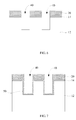
FIGS. 2 though 11 are schematic views of the structures corresponding to the process shown inFIG. 1 ; -
FIG. 12 is a flow chart of a method of manufacturing an injection-enhanced IGBT according to another embodiment; and -
FIG. 13 is a flow chart of a method of manufacturing an injection-enhanced IGBT according to yet another embodiment. - For the purpose of better understanding the above objects, features and advantages, embodiments of the present invention will be described in detail hereinafter in conjunction with the drawings. To facilitate the sufficient understanding of the invention, many details are set forth in the following description. However, the present invention may be implemented in other manners than those described herein, and similar extensions may be made by those skilled in the art without deviating from the spirit of the present invention. Therefore, the present invention is not limited by the embodiments disclosed hereinafter.
- As shown in
FIG. 1 , a method of manufacturing an injection-enhanced IGBT according to one embodiment includes the following steps: - S110, an N-type substrate is provided.
- Referring to
FIG. 2 , the specific resistance of the N-type substrate 12 is in a range of from about 0.01 Ω*cm to 200 Ω*cm. In practical application, the N-type substrate 12 having different specific resistances can be selected according to the IGBT product. The N-type substrate 12 can have a thickness in a range of from 100µm to 1000µm. - S115, a P-type doped
layer 14 is formed on the N-type substrate 12. - Referring to
FIG. 2 , a P-type dopedlayer 14 is formed by performing a P-type doping to the N-type substrate 12. Specifically, the P-type dopedlayer 14 can be formed by diffusion or ion implantation. The forming method of the P-type dopedlayer 14 is not limited herein. When the P-type dopedlayer 14 is formed by ion implantation, the implanted ion can be boron (B), and an implantation concentration of the ions can be from 1×10¹²/cm3 to 1×10²⁰/cm3. The energy of the implantation ion can be from 20KeV to 200KeV - S120, a hard layer is formed on the P-type doped layer.
- Referring to
FIG. 3 , thehard layer 20 can be made of silicon oxide or silicon nitride. The thickness of thehard layer 20 can be in a range of 500 angstrom to 100000 angstrom. In practical application, the thickness of thehard layer 20 can be other values. Thehard layer 20 covers the P-type dopedlayer 14. When thehard layer 20 is made of silicon oxide, thehard layer 20 can be formed by methods such as lower pressure SiO2 vapor deposition technology, furnace oxidation, rapid thermal annealing oxidation or in-situ vapor oxidation. When thehard layer 20 is made of silicon nitride, thehard layer 20 can be manufactured by chemical vapor deposition technology. - S130, a hard layer having a trench pattern is formed by etching the hard layer.
- The hard layer having the trench pattern is formed by adopting photolithography and etching method to etch the hard layer.
- The specific steps of adopting a photo-etching method to etch the hard layer to form the hard layer having the trench pattern is:
- Referring to
FIG. 4 , aphotoresist layer 30 is formed on thehard layer 20 first. And then, thephotoresist layer 30 is placed beneath an exposure equipment, a photo-mask having the trench pattern on its surface is adopted to perform a photo-mask exposure, the trench pattern on the photo-mask is transferred to thephotoresist layer 30, and then developing solution is adopted to remove the photoresist on the exposure region, thephotoresist layer 30 having the trench pattern is formed. Referring toFIG. 5 , thephotoresist layer 30 having the trench pattern is adopted as a mask, thehard layer 20 is etched to form thehard layer 20 having the trench pattern. - The
photoresist layer 30 can be formed by static drip or spin coating technology. - S140, a trench is formed by etching the P-type doped layer, and the trench extends into the N-type substrate.
- Referring to
FIG. 6 andFIG. 9 , in the embodiment, a depth of thetrench 40 extends through the P-type dopedlayer 14, and the depth of thetrench 40 is deeper than a thickness of the P-body 60 which is formed by performing a drive-in to the P-type dopedlayer 14. The depth of thetrench 40 can be in a range of 0.5µm to 15µm. In practical application, one skilled in the art can select the depth of thetrench 40 according to a specific condition. - After etching the
hard layer 20 to form thehard layer 20 having the trench pattern, and before forming thetrench 40 on the P-type dopedlayer 12, thephotoresist layer 30 can be removed. Thephotoresist layer 30 can also be removed after formingtrench 40 on the P-type dopedlayer 12. Thephotoresist layer 30 can be removed by dry stripping or wet stripping technology. The dry stripping technology adopts plasma to bombard the photoresist to remove thephotoresist layer 30. The wet stripping technology adopts cleaning solution to remove thephotoresist layer 30. The cleaning solution adopted by the wet stripping technology can be a mixed liquid of sulfuric acid and oxidizing agent. In other embodiments, the cleaning solution of the wet stripping technology can be other mixture material. It should be noted that, one skilled in the art can selectively adopt the dry stripping technology or the wet stripping technology to remove thephotoresist layer 30 according to a practical situation. - S150, an N-type doped layer is formed on a sidewall and a bottom of the trench.
- Referring to
FIG. 7 , in the embodiment, thehard layer 20 having the trench pattern is adopted as a mask, and the N-type dopedlayer 50 is formed on the sidewall and the bottom of thetrench 40 by a diffusion technology. - The temperature of the diffusion technology is from 800°C to 1250°C, the time period of the diffusion technology is from 10min to 300min, the diffusion source is an N-type dopant, such as B2O3, POCl3 or PH3. In the embodiment, the diffusion source is POCl3. The concentration of the N-type dopant of the N-type doped
layer 50 is from 1×10¹²/cm3 to 1×10²⁰/cm3. The category and concentration of dopant in the growth process can be controlled according to a specific requirement of the device. The N-type dopedlayer 50 has a thickness from 0.5µm to 20µm. - S160, the
hard layer 20 having the trench pattern is removed. When thehard layer 20 is an oxide, thehard layer 20 covering on the P-type dopedlayer 14 is removed by the plasma etching technology or by the buffer oxide etching technology, the structure after removing thehard layer 20 is shown asFIG. 8 . The buffer oxide etching technology can adopt a mixed solution of hydrofluoric acid (49%), water and ammonium fluoride to rinse thehard layer 20. In practical application, a removal rate of thehard layer 20 can be adjusted by adjusting concentrations of the hydrofluoric acid and the ammonium fluoride. - When the
hard layer 20 is nitride, thehard layer 20 can be removed by wet etching. - S170, the P-type dopant of the P-type doped layer and the N-type dopant of the N-type doped layer are driven-in together, the P-type dopant forms a P-type base region by diffusing, and the N-type dopant forms an N-type buffer layer by diffusing.
- Referring to
FIG. 9 , the drive-in allows the implanted N-type dopant and the P-type dopant to penetrate the silicon crystal in the N-type substrate 12 and form a desired junction depth in the N-type substrate 12, and form a P-type base region and an N-type buffer layer,. In the embodiment, the temperature of drive-in can be from 1100°C to 1280°C, the time period of drive-in can be from 20 min to 500 min. In practical application, the temperature and time period of the drive-in can be adjusted according to a specific requirement of the device. - S180, a gate oxide dielectric layer is formed on the surface of the trench.
- The operation for forming the gate oxide dielectric layer on the surface of the trench includes:
- First, a sacrificial oxide layer (not shown) is formed by oxidizing the surface of the
trench 40. Then, the sacrificial oxide layer is removed by etching. Subsequently, the surface of thetrench 40 is oxidized to form a gateoxide dielectric layer 80. The structure after forming a gateoxide dielectric layer 80 is shown asFIG. 10 . - Because many more defects are inevitably formed on the surface of the
trench 40 when etching the trench, it affects the quality of the gateoxide dielectric layer 80. Therefore, when the surface of thetrench 40 is oxidized to form a sacrificial oxide layer first, and then the sacrificial oxide layer is etched to be removed, and then the gateoxide dielectric layer 80 is formed by oxidization, it facilitates to improve the oneness of the material and the homogeneity of the gateoxide dielectric layer 40, and improving the quality of the gate oxide dielectric layer. - The sacrificial oxide layer can be formed by a dry oxidization or a wet oxidization.
- The sacrificial oxide layer can be removed by a wet etching.
- The gate
oxide dielectric layer 80 can be formed by a dry oxidization. The oxidizing method of the gateoxide dielectric layer 80 is not limited. For one skilled in the art, an appropriate oxidizing method of the gateoxide dielectric layer 80 can be selected according to a requirement of the quality of the gateoxide dielectric layer 80. A thickness of the gateoxide dielectric layer 80 can be in a range from 100 angstrom to 5000 angstrom, for example, the thickness is 1000 angstrom. - S190, a polysilicon layer is deposited in the trench on which the gate oxide dielectric layer is formed.
- The structure after depositing a polysilicon layer in the trench on which the gate oxide dielectric layer is formed and a back etching is shown as
FIG. 11 . The polysilicon layer can be formed by chemical vapor deposition, physical vapor deposition or other ways. In practical application, an appropriate deposition method can be selected according to a requirement. In the embodiment, thepolysilicon layer 90 can adopt a dry etching to back etch the polysilicon layer, to remove the redundant deposition. - A gate electrode is formed by performing subsequent processes to the
polysilicon layer 90. Subsequently, an emitting electrode and a collector electrode are formed by performing front processes, backgrind, back implantation, annealing, and back metallization and other steps to the device obtained by S190, an injection-enhanced IGBT is obtained. All technologies such as performing subsequent processes to the polysilicon layer 9 to form a gate electrode, front processes, backgrind, back implantation, annealing, and back metallization can adopt customary means in the technical field, and will not be limited hereby. - Above described method of manufacturing an injection-enhanced IGBT is merely directed to an operation including: forming a P-type doped layer on the surface of the N-type substrate first; performing an etching to the trench subsequently; and then forming an N-type doped layer by diffusion technology; and then performing a drive-in to the P-type dopant of the P-type doped layer and the N-type dopant of the N-type doped layer together. It is possible that performing an etching to the N-type substrate to form the trench first, and then forming a P-type doped layer on the surface of the N-type substrate; and then forming an N-type doped layer by diffusion technology; and then performing a drive-in to the P-type dopant of the P-type doped layer and the N-type dopant of the N-type doped layer together.
- As shown in
FIG. 12 , a method of manufacturing an injection-enhanced IGBT according to another embodiment, includes the following steps: - S210, an N-type substrate is provided.
- The N-type substrate provided in S210 is same as the N-type substrate provided in S 110.
- S215, a hard layer is formed on the N-type substrate.
- The hard layer in S215 is same as the hard layer in S120. The technology for forming the hard layer in S215 is same as the technology for forming the hard layer in S120
- S220, a hard layer having a trench pattern is formed by etching the hard layer.
- The technology of etching the hard layer to form a hard layer having the trench pattern in S220 is same as the technology of etching the hard layer to form a hard layer having the trench pattern in S130.
- S225, a trench is formed by etching the N-type substrate.
- The trench formed in S225 is same as the trench formed in S140.
- S230, an N-type doped layer is formed on a sidewall and a bottom of the trench.
- In the embodiment, the hard layer having the trench pattern formed in step S220 is adopted as a mask, and the N-type doped layer is formed on the sidewall and the bottom of the trench by diffusion technology. The diffusion technology in S230 is same as the diffusion technology in S150.
- S235, the hard layer having the trench pattern is removed.
- The technology of removing the hard layer having the trench pattern in S235 is same as the technology of removing the hard layer having the trench pattern in S160.
- S240, a mask layer is formed in the trench, and the mask layer fills the trench.
- In the embodiment, the mask layer can be made of photoresist. When the mask layer is made of photoresist, the photoresist layer can be formed by performing static drip or spin coating to the surface of the N-type substrate, the photoresist fills the trench, and the photoresist on the surface of the N-type substrate which forms no trench is removed, and the photoresist in the trench is reserved.
- S250, a P-type doped layer is formed on the surface of the N-type substrate which forms the trench.
- In the embodiment, the P-type doped layer is formed by ion implantation. The ion implantation technology is same as that in S115.
- S260, the mask layer is removed.
- When the mask layer is made of photoresist, the dry stripping technology and the wet stripping technology can be adopted to remove the mask layer. The dry stripping technology adopts plasma to bombard the photoresist to remove the mask layer. The wet stripping technology adopts cleaning solution to remove the
mask layer 30. The cleaning solution adopted by the wet stripping technology can be a mixed liquid of sulfuric acid and oxidizing agent. - S270, the P-type dopant of the P-type doped layer and the N-type dopant of the N-type doped layer are driven-in together, the P-type dopant forms a P-type base region by diffusing, and the N-type dopant forms an N-type buffer layer by diffusing.
- The operation in S270 is same as that in S170.
- S280, a gate oxide dielectric layer is formed on the surface of the trench.
- The operation in S280 is same as that in S180.
- S290, a polysilicon layer is deposited in the trench on which the gate oxide dielectric layer is formed.
- The operation in S290 is same as that in S190. A gate electrode is formed by performing subsequent processes to the polysilicon layer. Subsequently, an emitting electrode and a collector electrode are formed by performing front processes, backgrind, back implantation, annealing, and back metallization and so on to the device obtained by S290, an injection-enhanced IGBT is obtained. All technologies such as performing subsequent processes to the polysilicon layer to form a gate electrode, front processes, backgrind, back implantation, annealing, and back metallization can adopt customary means in the technical field, and will not be limited hereby.
- As shown in
FIG. 13 , a method of manufacturing an injection-enhanced IGBT according to another embodiment, includes the following steps: - S310, an N-type substrate is provided.
- The N-type substrate provided in S310 is same as the N-type substrate provided in S110.
- S315, a hard layer is formed on the N-type substrate.
- The hard layer in S315 is same as the hard layer in S120. The technology for forming the hard layer in S315 is same as the technology for forming the hard layer in S120
- S320, a hard layer having a trench pattern is formed by etching the hard layer.
- The technology of etching the hard layer to form a hard layer having the trench pattern in S320 is same as the technology of etching the hard layer to form a hard layer having the trench pattern in S130.
- S325, a trench is formed by etching the N-type substrate.
- The trench formed in S325 is same as the trench formed in S140.
- S330, the hard layer having the trench pattern is removed.
- The technology of removing the hard layer having the trench pattern in S330 is same as the technology of removing the hard layer having the trench pattern in S160.
- S335, a mask layer is formed in the trench, and the mask layer fills the trench.
- In the embodiment, the mask layer can be made of photoresist. When the mask layer is made of photoresist, the photoresist layer can be formed by performing static drip or spin coating to the surface of the N-type substrate, the photoresist fills the trench, and the photoresist on the surface of the N-type substrate which forms no trench is removed, and the photoresist in the trench is reserved.
- S340, a P-type doped layer is formed on the surface of the N-type substrate which forms the trench.
- In the embodiment, the P-type doped layer is formed by ion implantation. The ion implantation technology is same as that in S115.
- S350, the mask layer is removed.
- When the mask layer is made of photoresist, the dry stripping technology and the wet stripping technology can be adopted to remove the mask layer. The dry stripping technology adopts plasma to bombard the photoresist to remove the mask layer. The wet stripping technology adopts cleaning solution to remove the mask layer. The cleaning solution adopted by the wet stripping technology can be a mixed liquid of sulfuric acid and oxidizing agent.
- S360, an N-type doped layer is formed on a sidewall and a bottom of the trench.
- The N-type doped layer is formed on the sidewall and the bottom of the trench by diffusion technology. The diffusion technology in S360 is same as the diffusion technology in S150.
- S370, the P-type dopant of the P-type doped layer and the N-type dopant of the N-type doped layer are driven-in together, the P-type dopant forms a P-type base region by diffusing, and the N-type dopant forms an N-type buffer layer by diffusing.
- The operation in S370 is same as that in S170.
- S380, a gate oxide dielectric layer is formed on the surface of the trench.
- The operation in S380 is same as that in S180.
- S390, a polysilicon layer is deposited in the trench on which the gate oxide dielectric layer is formed.
- The operation in S390 is same as that in S190. A gate electrode is formed by performing subsequent processes to the polysilicon layer. Subsequently, an emitting electrode and a collector electrode are formed by performing front processes, backgrind, back implantation, annealing, and back metallization and so on to the device obtained by S390, an injection-enhanced IGBT is obtained. All technologies such as performing subsequent processes to the polysilicon layer to form a gate electrode, front processes, backgrind, back implantation, annealing, and back metallization can adopt customary means in the technical field, and will not be limited herein.
- In above described injection-enhanced IGBT, the P-type dopant of the P-type doped layer and the N-type dopant of the N-type doped layer are driven-in together to form a P-type base region, and an N-type buffer layer, only one drive-in process is required, the production cycle is shortened in comparison with a conventional method of manufacturing injection-enhanced IGBT. In the conventional method of manufacturing injection-enhanced IGBT, the implantation positions of the buffer layer and the body are the same, two drive-in processes are performed, causing the body to be diffused, and it is compensated by the P-type dopant and the N-type dopant, thus the resistance in the base region to be increased. In the method of manufacturing above described injection-enhanced IGBT, the implantation positions of the buffer layer and the doped layer are different, the P-type doped layer and the N-type doped layer are driven-in together, the P-type dopant and the N-type dopant are not required to compensate.
- The device manufactured by above described method of manufacturing an injection-enhanced IGBT can optimize the performance of the device, such as voltage drop saturation (VDSON).
- Although the invention is illustrated and described herein with reference to specific embodiments, the invention is not intended to be limited to the details shown. Rather, various modifications may be made in the details within the scope and range of equivalents of the claims and without departing from the invention.
Claims (10)
- A method of manufacturing an injection enhanced IGBT (Insulated Gate Bipolar Transistor), comprising steps as follow:providing an N-type substrate;forming a P-type doped layer on the N-type substrate;forming a hard layer on the P-type doped layer;etching the hard layer to form a hard layer having a trench pattern;etching the P-type doped layer to form a trench extending into the N-type substrate;forming an N-type doped layer on a sidewall and a bottom of the trench;removing the hard layer having the trench pattern;performing a drive-in to the P-type dopant of the P-type doped layer and the N-type dopant of the N-type doped layer together, the P-type dopant forming a P-type base region by diffusing, and the N-type dopant forming an N-type buffer layer by diffusing;forming a gate oxide dielectric layer on a surface of the trench; anddepositing a polysilicon layer in the trench on which the gate oxide dielectric layer is formed.
- The method of manufacturing the injection-enhanced IGBT according to claim 1, wherein the P-type doped layer is formed by ion implantation or diffusion.
- The method of manufacturing the injection-enhanced IGBT according to claim 2, wherein a concentration of P-type dopant in the P-type doped layer is from 1×10¹²/cm3 to 1×10²⁰/cm3.
- The method of manufacturing the injection-enhanced IGBT according to claim 1, wherein in the forming the N-type doped layer on the sidewall and the bottom of the trench, the hard layer is adopted as a mask, the N-type doped layer is formed by diffusion technology.
- The method of manufacturing the injection-enhanced IGBT according to claim 1, wherein a concentration of N-type dopant in the N-type doped layer is 1×10¹²/cm3 to 1×10²⁰/cm3.
- The method of manufacturing the injection-enhanced IGBT according to claim 1, wherein in the performing a drive-in to the P-type dopant of the P-type doped layer and the N-type dopant of the N-type doped layer together, a temperature of the drive-in is from 1100°C to 1280°C.
- The method of manufacturing the injection-enhanced IGBT according to claim 1, wherein in the performing a drive-in to the P-type dopant of the P-type doped layer and the N-type dopant of the N-type doped layer together, a time period of the drive-in is from 20 min to 500 min.
- The method of manufacturing the injection-enhanced IGBT according to claim 1, wherein the forming the gate oxide dielectric layer on the surface of the trench comprises:oxidizing the surface of the trench to form a sacrificial oxide layer;removing the sacrificial oxide layer by etching;oxidizing the surface of the trench to form the gate oxide dielectric layer.
- The method of manufacturing the injection-enhanced IGBT according to claim 1, wherein the hard layer is made of silicon oxide or silicon nitride.
- A method of manufacturing the injection-enhanced IGBT, comprising steps as follow:providing an N-type substrate;forming a hard layer on the N-type doped layer;etching the hard layer to form a hard layer having a trench pattern;etching the N-type doped layer to form a trench;forming an N-type doped layer on a sidewall and a bottom of the trench;removing the hard layer having the trench pattern;forming a mask layer in the trench, the mask layer filling the trench;forming a P-type doped layer on a surface of the N-type substrate which forms the trench;removing the mask layer;performing a drive-in to the P-type dopant of the P-type doped layer and the N-type dopant of the N-type doped layer together, the P-type dopant forming a P-type base region by diffusing, and the N-type dopant forming an N-type buffer layer by diffusing;forming a gate oxide dielectric layer on a surface of the trench; anddepositing a polysilicon layer in the trench on which the gate oxide dielectric layer is formed.
Applications Claiming Priority (2)
| Application Number | Priority Date | Filing Date | Title |
|---|---|---|---|
| CN201310312223.7A CN104347397B (en) | 2013-07-23 | 2013-07-23 | Inject the manufacture method of reinforced insulation grid bipolar transistor |
| PCT/CN2014/082816 WO2015010618A1 (en) | 2013-07-23 | 2014-07-23 | Method for manufacturing injection-enhanced insulated-gate bipolar transistor |
Publications (3)
| Publication Number | Publication Date |
|---|---|
| EP3026695A1 true EP3026695A1 (en) | 2016-06-01 |
| EP3026695A4 EP3026695A4 (en) | 2017-03-15 |
| EP3026695B1 EP3026695B1 (en) | 2019-09-11 |
Family
ID=52392738
Family Applications (1)
| Application Number | Title | Priority Date | Filing Date |
|---|---|---|---|
| EP14829488.7A Active EP3026695B1 (en) | 2013-07-23 | 2014-07-23 | Method for manufacturing injection-enhanced insulated-gate bipolar transistor |
Country Status (4)
| Country | Link |
|---|---|
| US (1) | US9583587B2 (en) |
| EP (1) | EP3026695B1 (en) |
| CN (1) | CN104347397B (en) |
| WO (1) | WO2015010618A1 (en) |
Families Citing this family (8)
| Publication number | Priority date | Publication date | Assignee | Title |
|---|---|---|---|---|
| CN106158650A (en) * | 2015-04-16 | 2016-11-23 | 中芯国际集成电路制造(上海)有限公司 | Transistor and forming method thereof |
| CN107527811B (en) * | 2016-06-21 | 2020-07-10 | 无锡华润上华科技有限公司 | Lateral insulated gate bipolar transistor and manufacturing method thereof |
| CN108933078B (en) * | 2017-05-25 | 2020-11-03 | 中芯国际集成电路制造(上海)有限公司 | Forming method and structure of doped region and IGBT device |
| US20200105874A1 (en) * | 2018-10-01 | 2020-04-02 | Ipower Semiconductor | Back side dopant activation in field stop igbt |
| CN109461767B (en) * | 2018-10-25 | 2022-03-29 | 深圳市金鑫城纸品有限公司 | Manufacturing method of super junction structure |
| CN112802742A (en) * | 2021-03-24 | 2021-05-14 | 上海华虹宏力半导体制造有限公司 | Method for manufacturing semiconductor device |
| CN115249616A (en) * | 2021-04-27 | 2022-10-28 | 无锡华润华晶微电子有限公司 | Insulated gate bipolar transistor and method of making the same |
| CN115692487B (en) * | 2021-07-29 | 2026-03-17 | 芯恩(青岛)集成电路有限公司 | A semiconductor power device and its fabrication method |
Family Cites Families (25)
| Publication number | Priority date | Publication date | Assignee | Title |
|---|---|---|---|---|
| KR100299912B1 (en) | 1998-02-03 | 2001-12-17 | 김덕중 | Method for fabricating insulating gate bipolar transistor |
| JP3833903B2 (en) * | 2000-07-11 | 2006-10-18 | 株式会社東芝 | Manufacturing method of semiconductor device |
| US6489204B1 (en) * | 2001-08-20 | 2002-12-03 | Episil Technologies, Inc. | Save MOS device |
| US6919248B2 (en) * | 2003-03-14 | 2005-07-19 | International Rectifier Corporation | Angled implant for shorter trench emitter |
| JP4091921B2 (en) * | 2004-02-16 | 2008-05-28 | 松下電器産業株式会社 | Semiconductor device and manufacturing method thereof |
| JP4182986B2 (en) * | 2006-04-19 | 2008-11-19 | トヨタ自動車株式会社 | Semiconductor device and manufacturing method thereof |
| JP5261927B2 (en) * | 2006-12-11 | 2013-08-14 | パナソニック株式会社 | Semiconductor device |
| US7968940B2 (en) * | 2007-07-05 | 2011-06-28 | Anpec Electronics Corporation | Insulated gate bipolar transistor device comprising a depletion-mode MOSFET |
| JP5707681B2 (en) * | 2009-03-04 | 2015-04-30 | 富士電機株式会社 | Semiconductor device and manufacturing method thereof |
| JP2010219361A (en) * | 2009-03-18 | 2010-09-30 | Toshiba Corp | Semiconductor device and manufacturing method thereof |
| US8299494B2 (en) * | 2009-06-12 | 2012-10-30 | Alpha & Omega Semiconductor, Inc. | Nanotube semiconductor devices |
| CN102487078A (en) * | 2010-12-06 | 2012-06-06 | 无锡华润上华半导体有限公司 | Insulated gate bipolar power tube and manufacture method thereof |
| JP5969771B2 (en) * | 2011-05-16 | 2016-08-17 | ルネサスエレクトロニクス株式会社 | IE type trench gate IGBT |
| US8748973B2 (en) * | 2011-05-19 | 2014-06-10 | Anpec Electronics Corporation | Super junction transistor and fabrication method thereof |
| CN102856192B (en) * | 2011-06-27 | 2015-05-13 | 中国科学院微电子研究所 | IGBT device and manufacturing method thereof |
| US8643097B2 (en) * | 2011-08-09 | 2014-02-04 | United Microelectronics Corporation | Trench-gate metal oxide semiconductor device and fabricating method thereof |
| CN103094324B (en) * | 2011-11-08 | 2016-03-23 | 无锡华润上华半导体有限公司 | Trench-type insulated gate bipolar transistor and preparation method thereof |
| TWI470802B (en) * | 2011-12-21 | 2015-01-21 | 財團法人工業技術研究院 | Trench type MOS transistor crystal element and manufacturing method thereof |
| US9087894B2 (en) * | 2012-02-10 | 2015-07-21 | Panasonic Intellectual Property Management Co., Ltd. | Semiconductor device and method of manufacturing the device |
| US8975662B2 (en) * | 2012-06-14 | 2015-03-10 | Infineon Technologies Austria Ag | Method of manufacturing a semiconductor device using an impurity source containing a metallic recombination element and semiconductor device |
| CN103035720B (en) * | 2012-09-05 | 2015-02-04 | 上海华虹宏力半导体制造有限公司 | Super junction device and manufacturing method thereof |
| US8878238B2 (en) * | 2012-10-01 | 2014-11-04 | Pakal Technologies Llc | MCT device with base-width-determined latching and non-latching states |
| CN103022099B (en) * | 2013-01-10 | 2016-05-04 | 江苏物联网研究发展中心 | A kind of IGBT collector structure and its preparation method |
| DE112014003712T5 (en) * | 2013-12-16 | 2016-04-28 | Fuji Electric Co., Ltd. | Semiconductor device and method of manufacturing a semiconductor device |
| JP6365165B2 (en) * | 2014-09-18 | 2018-08-01 | 富士電機株式会社 | Manufacturing method of semiconductor device |
-
2013
- 2013-07-23 CN CN201310312223.7A patent/CN104347397B/en active Active
-
2014
- 2014-07-23 WO PCT/CN2014/082816 patent/WO2015010618A1/en not_active Ceased
- 2014-07-23 EP EP14829488.7A patent/EP3026695B1/en active Active
- 2014-07-23 US US14/902,220 patent/US9583587B2/en active Active
Non-Patent Citations (1)
| Title |
|---|
| See references of WO2015010618A1 * |
Also Published As
| Publication number | Publication date |
|---|---|
| US9583587B2 (en) | 2017-02-28 |
| WO2015010618A1 (en) | 2015-01-29 |
| CN104347397A (en) | 2015-02-11 |
| EP3026695B1 (en) | 2019-09-11 |
| EP3026695A4 (en) | 2017-03-15 |
| CN104347397B (en) | 2018-02-06 |
| US20160372573A1 (en) | 2016-12-22 |
Similar Documents
| Publication | Publication Date | Title |
|---|---|---|
| EP3026695B1 (en) | Method for manufacturing injection-enhanced insulated-gate bipolar transistor | |
| KR100218260B1 (en) | Manufacturing method of trench gate type MOS transistor | |
| JP2016537816A (en) | Method for selectively etching a mask deposited on a silicon substrate | |
| CN109216276A (en) | A kind of metal-oxide-semiconductor and its manufacturing method | |
| CN102136425A (en) | P-channel depletion MOS (metal oxide semiconductor) transistor and preparation method thereof | |
| JP2006059843A (en) | Semiconductor device and manufacturing method thereof | |
| CN107527811B (en) | Lateral insulated gate bipolar transistor and manufacturing method thereof | |
| CN102915975A (en) | Method for manufacturing BJT (bipolar junction transistor) and BiCMOS (bipolar complementary metal oxide semiconductor) | |
| CN102122643B (en) | Method for manufacturing bipolar junction transistor | |
| CN108538911B (en) | Optimized L-type tunneling field effect transistor and preparation method thereof | |
| CN102087977B (en) | Vertical negative-positive-negative (NPN) transistor and manufacturing method thereof | |
| CN102254933A (en) | PN junction isolating structure and forming method thereof | |
| CN104637811B (en) | Transistor fabrication process and transistor | |
| CN107305839B (en) | Method for preventing self-doping effect | |
| CN104347396B (en) | Inject the manufacture method of reinforced insulation grid bipolar transistor | |
| US7572708B1 (en) | Utilization of doped glass on the sidewall of the emitter window in a bipolar transistor structure | |
| CN102693915A (en) | Manufacturing method for MOS transistor | |
| JP2014508408A (en) | Semiconductor device and related manufacturing method | |
| CN106783606A (en) | Power semiconductor and preparation method thereof | |
| CN106981421B (en) | How to make a triode base | |
| CN107104049A (en) | The preparation method and radio frequency triode of radio frequency triode | |
| CN106298868A (en) | A kind of super node MOSFET structure and preparation method thereof | |
| CN104637810A (en) | Method for manufacturing emitter region of transistor | |
| KR100402106B1 (en) | Manufacturing Method of Semiconductor Device | |
| JP2016004952A (en) | Semiconductor device manufacturing method |
Legal Events
| Date | Code | Title | Description |
|---|---|---|---|
| PUAI | Public reference made under article 153(3) epc to a published international application that has entered the european phase |
Free format text: ORIGINAL CODE: 0009012 |
|
| 17P | Request for examination filed |
Effective date: 20151230 |
|
| AK | Designated contracting states |
Kind code of ref document: A1 Designated state(s): AL AT BE BG CH CY CZ DE DK EE ES FI FR GB GR HR HU IE IS IT LI LT LU LV MC MK MT NL NO PL PT RO RS SE SI SK SM TR |
|
| AX | Request for extension of the european patent |
Extension state: BA ME |
|
| DAX | Request for extension of the european patent (deleted) | ||
| A4 | Supplementary search report drawn up and despatched |
Effective date: 20170209 |
|
| RIC1 | Information provided on ipc code assigned before grant |
Ipc: H01L 29/78 20060101ALI20170203BHEP Ipc: H01L 29/739 20060101ALI20170203BHEP Ipc: H01L 21/331 20060101AFI20170203BHEP |
|
| GRAP | Despatch of communication of intention to grant a patent |
Free format text: ORIGINAL CODE: EPIDOSNIGR1 |
|
| STAA | Information on the status of an ep patent application or granted ep patent |
Free format text: STATUS: GRANT OF PATENT IS INTENDED |
|
| INTG | Intention to grant announced |
Effective date: 20190215 |
|
| GRAS | Grant fee paid |
Free format text: ORIGINAL CODE: EPIDOSNIGR3 |
|
| RAP1 | Party data changed (applicant data changed or rights of an application transferred) |
Owner name: CSMC TECHNOLOGIES FAB2 CO., LTD. |
|
| GRAA | (expected) grant |
Free format text: ORIGINAL CODE: 0009210 |
|
| STAA | Information on the status of an ep patent application or granted ep patent |
Free format text: STATUS: THE PATENT HAS BEEN GRANTED |
|
| AK | Designated contracting states |
Kind code of ref document: B1 Designated state(s): AL AT BE BG CH CY CZ DE DK EE ES FI FR GB GR HR HU IE IS IT LI LT LU LV MC MK MT NL NO PL PT RO RS SE SI SK SM TR |
|
| REG | Reference to a national code |
Ref country code: GB Ref legal event code: FG4D |
|
| REG | Reference to a national code |
Ref country code: CH Ref legal event code: EP |
|
| REG | Reference to a national code |
Ref country code: AT Ref legal event code: REF Ref document number: 1179568 Country of ref document: AT Kind code of ref document: T Effective date: 20190915 |
|
| REG | Reference to a national code |
Ref country code: DE Ref legal event code: R096 Ref document number: 602014053583 Country of ref document: DE Ref country code: IE Ref legal event code: FG4D |
|
| REG | Reference to a national code |
Ref country code: NL Ref legal event code: FP |
|
| REG | Reference to a national code |
Ref country code: LT Ref legal event code: MG4D |
|
| PG25 | Lapsed in a contracting state [announced via postgrant information from national office to epo] |
Ref country code: NO Free format text: LAPSE BECAUSE OF FAILURE TO SUBMIT A TRANSLATION OF THE DESCRIPTION OR TO PAY THE FEE WITHIN THE PRESCRIBED TIME-LIMIT Effective date: 20191211 Ref country code: FI Free format text: LAPSE BECAUSE OF FAILURE TO SUBMIT A TRANSLATION OF THE DESCRIPTION OR TO PAY THE FEE WITHIN THE PRESCRIBED TIME-LIMIT Effective date: 20190911 Ref country code: SE Free format text: LAPSE BECAUSE OF FAILURE TO SUBMIT A TRANSLATION OF THE DESCRIPTION OR TO PAY THE FEE WITHIN THE PRESCRIBED TIME-LIMIT Effective date: 20190911 Ref country code: BG Free format text: LAPSE BECAUSE OF FAILURE TO SUBMIT A TRANSLATION OF THE DESCRIPTION OR TO PAY THE FEE WITHIN THE PRESCRIBED TIME-LIMIT Effective date: 20191211 Ref country code: HR Free format text: LAPSE BECAUSE OF FAILURE TO SUBMIT A TRANSLATION OF THE DESCRIPTION OR TO PAY THE FEE WITHIN THE PRESCRIBED TIME-LIMIT Effective date: 20190911 Ref country code: LT Free format text: LAPSE BECAUSE OF FAILURE TO SUBMIT A TRANSLATION OF THE DESCRIPTION OR TO PAY THE FEE WITHIN THE PRESCRIBED TIME-LIMIT Effective date: 20190911 |
|
| PG25 | Lapsed in a contracting state [announced via postgrant information from national office to epo] |
Ref country code: AL Free format text: LAPSE BECAUSE OF FAILURE TO SUBMIT A TRANSLATION OF THE DESCRIPTION OR TO PAY THE FEE WITHIN THE PRESCRIBED TIME-LIMIT Effective date: 20190911 Ref country code: RS Free format text: LAPSE BECAUSE OF FAILURE TO SUBMIT A TRANSLATION OF THE DESCRIPTION OR TO PAY THE FEE WITHIN THE PRESCRIBED TIME-LIMIT Effective date: 20190911 Ref country code: GR Free format text: LAPSE BECAUSE OF FAILURE TO SUBMIT A TRANSLATION OF THE DESCRIPTION OR TO PAY THE FEE WITHIN THE PRESCRIBED TIME-LIMIT Effective date: 20191212 Ref country code: LV Free format text: LAPSE BECAUSE OF FAILURE TO SUBMIT A TRANSLATION OF THE DESCRIPTION OR TO PAY THE FEE WITHIN THE PRESCRIBED TIME-LIMIT Effective date: 20190911 Ref country code: ES Free format text: LAPSE BECAUSE OF FAILURE TO SUBMIT A TRANSLATION OF THE DESCRIPTION OR TO PAY THE FEE WITHIN THE PRESCRIBED TIME-LIMIT Effective date: 20190911 |
|
| REG | Reference to a national code |
Ref country code: AT Ref legal event code: MK05 Ref document number: 1179568 Country of ref document: AT Kind code of ref document: T Effective date: 20190911 |
|
| PG25 | Lapsed in a contracting state [announced via postgrant information from national office to epo] |
Ref country code: PL Free format text: LAPSE BECAUSE OF FAILURE TO SUBMIT A TRANSLATION OF THE DESCRIPTION OR TO PAY THE FEE WITHIN THE PRESCRIBED TIME-LIMIT Effective date: 20190911 Ref country code: PT Free format text: LAPSE BECAUSE OF FAILURE TO SUBMIT A TRANSLATION OF THE DESCRIPTION OR TO PAY THE FEE WITHIN THE PRESCRIBED TIME-LIMIT Effective date: 20200113 Ref country code: RO Free format text: LAPSE BECAUSE OF FAILURE TO SUBMIT A TRANSLATION OF THE DESCRIPTION OR TO PAY THE FEE WITHIN THE PRESCRIBED TIME-LIMIT Effective date: 20190911 Ref country code: AT Free format text: LAPSE BECAUSE OF FAILURE TO SUBMIT A TRANSLATION OF THE DESCRIPTION OR TO PAY THE FEE WITHIN THE PRESCRIBED TIME-LIMIT Effective date: 20190911 Ref country code: EE Free format text: LAPSE BECAUSE OF FAILURE TO SUBMIT A TRANSLATION OF THE DESCRIPTION OR TO PAY THE FEE WITHIN THE PRESCRIBED TIME-LIMIT Effective date: 20190911 Ref country code: IT Free format text: LAPSE BECAUSE OF FAILURE TO SUBMIT A TRANSLATION OF THE DESCRIPTION OR TO PAY THE FEE WITHIN THE PRESCRIBED TIME-LIMIT Effective date: 20190911 |
|
| PG25 | Lapsed in a contracting state [announced via postgrant information from national office to epo] |
Ref country code: CZ Free format text: LAPSE BECAUSE OF FAILURE TO SUBMIT A TRANSLATION OF THE DESCRIPTION OR TO PAY THE FEE WITHIN THE PRESCRIBED TIME-LIMIT Effective date: 20190911 Ref country code: SM Free format text: LAPSE BECAUSE OF FAILURE TO SUBMIT A TRANSLATION OF THE DESCRIPTION OR TO PAY THE FEE WITHIN THE PRESCRIBED TIME-LIMIT Effective date: 20190911 Ref country code: SK Free format text: LAPSE BECAUSE OF FAILURE TO SUBMIT A TRANSLATION OF THE DESCRIPTION OR TO PAY THE FEE WITHIN THE PRESCRIBED TIME-LIMIT Effective date: 20190911 Ref country code: IS Free format text: LAPSE BECAUSE OF FAILURE TO SUBMIT A TRANSLATION OF THE DESCRIPTION OR TO PAY THE FEE WITHIN THE PRESCRIBED TIME-LIMIT Effective date: 20200224 |
|
| REG | Reference to a national code |
Ref country code: DE Ref legal event code: R097 Ref document number: 602014053583 Country of ref document: DE |
|
| PLBE | No opposition filed within time limit |
Free format text: ORIGINAL CODE: 0009261 |
|
| STAA | Information on the status of an ep patent application or granted ep patent |
Free format text: STATUS: NO OPPOSITION FILED WITHIN TIME LIMIT |
|
| PG2D | Information on lapse in contracting state deleted |
Ref country code: IS |
|
| PG25 | Lapsed in a contracting state [announced via postgrant information from national office to epo] |
Ref country code: IS Free format text: LAPSE BECAUSE OF FAILURE TO SUBMIT A TRANSLATION OF THE DESCRIPTION OR TO PAY THE FEE WITHIN THE PRESCRIBED TIME-LIMIT Effective date: 20200112 Ref country code: DK Free format text: LAPSE BECAUSE OF FAILURE TO SUBMIT A TRANSLATION OF THE DESCRIPTION OR TO PAY THE FEE WITHIN THE PRESCRIBED TIME-LIMIT Effective date: 20190911 |
|
| 26N | No opposition filed |
Effective date: 20200615 |
|
| PG25 | Lapsed in a contracting state [announced via postgrant information from national office to epo] |
Ref country code: SI Free format text: LAPSE BECAUSE OF FAILURE TO SUBMIT A TRANSLATION OF THE DESCRIPTION OR TO PAY THE FEE WITHIN THE PRESCRIBED TIME-LIMIT Effective date: 20190911 |
|
| PG25 | Lapsed in a contracting state [announced via postgrant information from national office to epo] |
Ref country code: MC Free format text: LAPSE BECAUSE OF FAILURE TO SUBMIT A TRANSLATION OF THE DESCRIPTION OR TO PAY THE FEE WITHIN THE PRESCRIBED TIME-LIMIT Effective date: 20190911 |
|
| REG | Reference to a national code |
Ref country code: CH Ref legal event code: PL |
|
| REG | Reference to a national code |
Ref country code: BE Ref legal event code: MM Effective date: 20200731 |
|
| PG25 | Lapsed in a contracting state [announced via postgrant information from national office to epo] |
Ref country code: LU Free format text: LAPSE BECAUSE OF NON-PAYMENT OF DUE FEES Effective date: 20200723 Ref country code: LI Free format text: LAPSE BECAUSE OF NON-PAYMENT OF DUE FEES Effective date: 20200731 Ref country code: CH Free format text: LAPSE BECAUSE OF NON-PAYMENT OF DUE FEES Effective date: 20200731 |
|
| PG25 | Lapsed in a contracting state [announced via postgrant information from national office to epo] |
Ref country code: BE Free format text: LAPSE BECAUSE OF NON-PAYMENT OF DUE FEES Effective date: 20200731 |
|
| PG25 | Lapsed in a contracting state [announced via postgrant information from national office to epo] |
Ref country code: IE Free format text: LAPSE BECAUSE OF NON-PAYMENT OF DUE FEES Effective date: 20200723 |
|
| PG25 | Lapsed in a contracting state [announced via postgrant information from national office to epo] |
Ref country code: TR Free format text: LAPSE BECAUSE OF FAILURE TO SUBMIT A TRANSLATION OF THE DESCRIPTION OR TO PAY THE FEE WITHIN THE PRESCRIBED TIME-LIMIT Effective date: 20190911 Ref country code: MT Free format text: LAPSE BECAUSE OF FAILURE TO SUBMIT A TRANSLATION OF THE DESCRIPTION OR TO PAY THE FEE WITHIN THE PRESCRIBED TIME-LIMIT Effective date: 20190911 Ref country code: CY Free format text: LAPSE BECAUSE OF FAILURE TO SUBMIT A TRANSLATION OF THE DESCRIPTION OR TO PAY THE FEE WITHIN THE PRESCRIBED TIME-LIMIT Effective date: 20190911 |
|
| PG25 | Lapsed in a contracting state [announced via postgrant information from national office to epo] |
Ref country code: MK Free format text: LAPSE BECAUSE OF FAILURE TO SUBMIT A TRANSLATION OF THE DESCRIPTION OR TO PAY THE FEE WITHIN THE PRESCRIBED TIME-LIMIT Effective date: 20190911 |
|
| REG | Reference to a national code |
Ref country code: DE Ref legal event code: R079 Ref document number: 602014053583 Country of ref document: DE Free format text: PREVIOUS MAIN CLASS: H01L0021331000 Ipc: H10D0012010000 |
|
| PGFP | Annual fee paid to national office [announced via postgrant information from national office to epo] |
Ref country code: GB Payment date: 20250625 Year of fee payment: 12 |
|
| PGFP | Annual fee paid to national office [announced via postgrant information from national office to epo] |
Ref country code: NL Payment date: 20250626 Year of fee payment: 12 |
|
| PGFP | Annual fee paid to national office [announced via postgrant information from national office to epo] |
Ref country code: FR Payment date: 20250626 Year of fee payment: 12 |
|
| PGFP | Annual fee paid to national office [announced via postgrant information from national office to epo] |
Ref country code: DE Payment date: 20250722 Year of fee payment: 12 |