EP3025195B1 - Patterned stamp manufacturing method, patterned stamp and patterned stamp imprinting method - Google Patents
Patterned stamp manufacturing method, patterned stamp and patterned stamp imprinting method Download PDFInfo
- Publication number
- EP3025195B1 EP3025195B1 EP14744033.3A EP14744033A EP3025195B1 EP 3025195 B1 EP3025195 B1 EP 3025195B1 EP 14744033 A EP14744033 A EP 14744033A EP 3025195 B1 EP3025195 B1 EP 3025195B1
- Authority
- EP
- European Patent Office
- Prior art keywords
- layer
- stamp
- patterned
- contoured surface
- pattern
- Prior art date
- Legal status (The legal status is an assumption and is not a legal conclusion. Google has not performed a legal analysis and makes no representation as to the accuracy of the status listed.)
- Active
Links
- 238000000034 method Methods 0.000 title claims description 61
- 238000004519 manufacturing process Methods 0.000 title claims description 15
- 239000000463 material Substances 0.000 claims description 72
- 239000002243 precursor Substances 0.000 claims description 28
- 239000004205 dimethyl polysiloxane Substances 0.000 claims description 25
- 229920000435 poly(dimethylsiloxane) Polymers 0.000 claims description 25
- 229920001971 elastomer Polymers 0.000 claims description 14
- -1 polydimethylsiloxane Polymers 0.000 claims description 12
- 239000007788 liquid Substances 0.000 claims description 11
- 238000001459 lithography Methods 0.000 claims description 10
- 238000000059 patterning Methods 0.000 claims description 9
- 239000012530 fluid Substances 0.000 claims description 7
- 238000004987 plasma desorption mass spectroscopy Methods 0.000 claims description 4
- 235000013870 dimethyl polysiloxane Nutrition 0.000 claims 2
- KPUWHANPEXNPJT-UHFFFAOYSA-N disiloxane Chemical class [SiH3]O[SiH3] KPUWHANPEXNPJT-UHFFFAOYSA-N 0.000 claims 1
- CXQXSVUQTKDNFP-UHFFFAOYSA-N octamethyltrisiloxane Chemical compound C[Si](C)(C)O[Si](C)(C)O[Si](C)(C)C CXQXSVUQTKDNFP-UHFFFAOYSA-N 0.000 claims 1
- 229920001296 polysiloxane Polymers 0.000 description 10
- 238000007711 solidification Methods 0.000 description 10
- 230000008023 solidification Effects 0.000 description 10
- 239000011521 glass Substances 0.000 description 9
- 239000000758 substrate Substances 0.000 description 8
- 239000000203 mixture Substances 0.000 description 5
- 239000000853 adhesive Substances 0.000 description 4
- 230000001070 adhesive effect Effects 0.000 description 4
- 230000015572 biosynthetic process Effects 0.000 description 4
- 238000006243 chemical reaction Methods 0.000 description 4
- 230000008901 benefit Effects 0.000 description 3
- 230000008021 deposition Effects 0.000 description 3
- 230000003287 optical effect Effects 0.000 description 3
- 239000004065 semiconductor Substances 0.000 description 3
- 238000012546 transfer Methods 0.000 description 3
- 239000007943 implant Substances 0.000 description 2
- 238000002174 soft lithography Methods 0.000 description 2
- 229910002704 AlGaN Inorganic materials 0.000 description 1
- 229910000577 Silicon-germanium Inorganic materials 0.000 description 1
- 238000013459 approach Methods 0.000 description 1
- 229920001400 block copolymer Polymers 0.000 description 1
- 210000000988 bone and bone Anatomy 0.000 description 1
- 230000010478 bone regeneration Effects 0.000 description 1
- 239000013590 bulk material Substances 0.000 description 1
- 238000011109 contamination Methods 0.000 description 1
- 230000002596 correlated effect Effects 0.000 description 1
- 230000007547 defect Effects 0.000 description 1
- 230000001419 dependent effect Effects 0.000 description 1
- 238000013461 design Methods 0.000 description 1
- 239000000806 elastomer Substances 0.000 description 1
- 238000010894 electron beam technology Methods 0.000 description 1
- 238000005530 etching Methods 0.000 description 1
- 230000010354 integration Effects 0.000 description 1
- 238000000025 interference lithography Methods 0.000 description 1
- 239000012705 liquid precursor Substances 0.000 description 1
- 230000000873 masking effect Effects 0.000 description 1
- 239000002184 metal Substances 0.000 description 1
- 238000004377 microelectronic Methods 0.000 description 1
- 238000000465 moulding Methods 0.000 description 1
- 238000001127 nanoimprint lithography Methods 0.000 description 1
- 239000002070 nanowire Substances 0.000 description 1
- 230000000149 penetrating effect Effects 0.000 description 1
- 229920000642 polymer Polymers 0.000 description 1
- 230000005855 radiation Effects 0.000 description 1
- 230000007261 regionalization Effects 0.000 description 1
- 238000001878 scanning electron micrograph Methods 0.000 description 1
- 238000007789 sealing Methods 0.000 description 1
- 125000006850 spacer group Chemical group 0.000 description 1
- 229920001935 styrene-ethylene-butadiene-styrene Polymers 0.000 description 1
- 238000012360 testing method Methods 0.000 description 1
- 230000017423 tissue regeneration Effects 0.000 description 1
Images


Classifications
-
- B—PERFORMING OPERATIONS; TRANSPORTING
- B41—PRINTING; LINING MACHINES; TYPEWRITERS; STAMPS
- B41N—PRINTING PLATES OR FOILS; MATERIALS FOR SURFACES USED IN PRINTING MACHINES FOR PRINTING, INKING, DAMPING, OR THE LIKE; PREPARING SUCH SURFACES FOR USE AND CONSERVING THEM
- B41N1/00—Printing plates or foils; Materials therefor
- B41N1/12—Printing plates or foils; Materials therefor non-metallic other than stone, e.g. printing plates or foils comprising inorganic materials in an organic matrix
- B41N1/14—Lithographic printing foils
-
- B—PERFORMING OPERATIONS; TRANSPORTING
- B29—WORKING OF PLASTICS; WORKING OF SUBSTANCES IN A PLASTIC STATE IN GENERAL
- B29C—SHAPING OR JOINING OF PLASTICS; SHAPING OF MATERIAL IN A PLASTIC STATE, NOT OTHERWISE PROVIDED FOR; AFTER-TREATMENT OF THE SHAPED PRODUCTS, e.g. REPAIRING
- B29C59/00—Surface shaping of articles, e.g. embossing; Apparatus therefor
- B29C59/02—Surface shaping of articles, e.g. embossing; Apparatus therefor by mechanical means, e.g. pressing
-
- B—PERFORMING OPERATIONS; TRANSPORTING
- B41—PRINTING; LINING MACHINES; TYPEWRITERS; STAMPS
- B41C—PROCESSES FOR THE MANUFACTURE OR REPRODUCTION OF PRINTING SURFACES
- B41C3/00—Reproduction or duplicating of printing formes
- B41C3/04—Reproduction or duplicating of printing formes to produce rubber printing blocks
-
- B—PERFORMING OPERATIONS; TRANSPORTING
- B41—PRINTING; LINING MACHINES; TYPEWRITERS; STAMPS
- B41F—PRINTING MACHINES OR PRESSES
- B41F7/00—Rotary lithographic machines
-
- B—PERFORMING OPERATIONS; TRANSPORTING
- B41—PRINTING; LINING MACHINES; TYPEWRITERS; STAMPS
- B41K—STAMPS; STAMPING OR NUMBERING APPARATUS OR DEVICES
- B41K1/00—Portable hand-operated devices without means for supporting or locating the articles to be stamped, i.e. hand stamps; Inking devices or other accessories therefor
- B41K1/26—Portable hand-operated devices without means for supporting or locating the articles to be stamped, i.e. hand stamps; Inking devices or other accessories therefor with stamping surfaces adapted for application to non-flat surfaces
- B41K1/28—Portable hand-operated devices without means for supporting or locating the articles to be stamped, i.e. hand stamps; Inking devices or other accessories therefor with stamping surfaces adapted for application to non-flat surfaces flexible
-
- G—PHYSICS
- G03—PHOTOGRAPHY; CINEMATOGRAPHY; ANALOGOUS TECHNIQUES USING WAVES OTHER THAN OPTICAL WAVES; ELECTROGRAPHY; HOLOGRAPHY
- G03F—PHOTOMECHANICAL PRODUCTION OF TEXTURED OR PATTERNED SURFACES, e.g. FOR PRINTING, FOR PROCESSING OF SEMICONDUCTOR DEVICES; MATERIALS THEREFOR; ORIGINALS THEREFOR; APPARATUS SPECIALLY ADAPTED THEREFOR
- G03F7/00—Photomechanical, e.g. photolithographic, production of textured or patterned surfaces, e.g. printing surfaces; Materials therefor, e.g. comprising photoresists; Apparatus specially adapted therefor
- G03F7/0002—Lithographic processes using patterning methods other than those involving the exposure to radiation, e.g. by stamping
Definitions
- the present invention relates to a method of manufacturing a patterned stamp for patterning a contoured surface.
- the present invention further relates to such a patterned stamp.
- the present invention yet further relates to a method of patterning a contoured surface using such a stamp.
- the present invention yet further relates to an article obtained from this patterning method.
- Imprint lithography is a technique in which a patterned layer such as a masking layer is formed on a substrate such as a semiconductor substrate or as an optical layer by the deposition of a curable imprintable medium.
- the curable imprintable medium is subsequently patterned by imprinting the medium with a patterned stamp, after which the curable imprintable medium is solidified e.g. when exposed to light, e.g. UV-light to initiate the curing reaction in the medium.
- the stamp is removed from the medium to leave a patterned layer, e.g. on the semiconductor substrate or on a carrier of such an optical layer.
- a promising prospect of imprint lithography is that it can be used for forming nanoscale patterns on so-called 2.5D surfaces, i.e. contoured surfaces, which for instance may comprise one or more protrusions, e.g. curved protrusions, emanating from a mainly planar surface.
- Such techniques may be used to pattern photo-voltaic solar cells, nanowires, VECSEL lasers, medical implants and so on, e.g. by creating nanoscale patterns on optical elements, e.g. lenses or on medical implants, e.g. to stimulate bone or tissue regeneration.
- a planar pliable patterned stamp such as a polysiloxane-based rubber-like stamp, is typically deformed onto the contoured surface such that the stamp pattern is brought into contact with the contoured surface to be patterned.
- a stamp is shown in US 2008/0011934 A1 .
- BAHADOR FARSHIAN ET AL "Soft UV-nanoimprint lithography on non-planar surfaces", MICROELECTRONIC ENGINEERING, ELSEVIER PUBLISHERS BV., AMSTERDAM, NL, vol. 88, no. 11, 20 July 2011 (2011-07-20), pages 3287-3292 , and US 2010/109203 A1 relate to imprinting onto a substrate with a contoured surface.
- the present invention seeks to provide a method of manufacturing a patterned stamp for patterning a contoured surface in a more accurate manner.
- the present invention further seeks to provide a patterned stamp for patterning a contoured surface in a more accurate manner.
- the present invention further seeks to provide a method of patterning a contoured surface in a more accurate manner using such a stamp.
- the present invention yet further seeks to provide an article comprising a more accurately patterned contoured surface.
- a method of manufacturing a patterned stamp for patterning a contoured surface By providing a thin pliable patterned stamp layer over the contoured surface to be patterned, the stamp layer can be brought into contact with every aspect of the contoured surface due to the fact that the bulk support of the stamp that gives the stamp its structural integrity is not yet present. Indeed, this structural integrity limits the pliability of a stamp having a pattern of features extending from a planar surface. Consequently, the absence of the structural integrity provided by the support layer ensures that a good contact between the pattern of features and the contoured surface can be achieved.
- the subsequent formation of the support layer on the stamp layer fixates the patterned surface of the stamp into a contoured stamp surface carrying a pattern of features that complements the contoured surface to be imprinted, thereby providing a patterned stamp suitable for use in the imprint lithography of such contoured surfaces.
- the step of forcing the pliable stamp layer onto the contoured surface comprises placing the contoured surface with the pliable stamp layer in a vacuum chamber; and reducing the pressure in said vacuum chamber to force the pliable stamp layer onto the contoured surface. This ensures an even more intimate fit between the stamp layer and the contoured surface, thereby further improving the matching of the stamp to the contoured surface.
- the step of forcing the pliable stamp layer onto the contoured surface may comprise applying an overpressure to the pliable stamp layer to force the pliable stamp layer onto the contoured surface.
- the solidifying step comprises grafting the support layer onto the pliable stamp layer. This further improves the integration of the stamp layer into the support layer, thereby providing a stamp with excellent structural integrity. This may for instance be achieved if the stamp layer and the support layer comprise a rubbery curable material, such as a polysiloxane-based material.
- a rubbery curable material such as a polysiloxane-based material.
- a particularly suitable polysiloxane-based material is polydimethylsiloxane (PDMS).
- PDMS polydimethylsiloxane
- the features of the stamp layer may alter during the manufacturing of the stamp, such that the actual pattern of the stamp may deviate from its intended pattern.
- Several embodiments of the present method are directed to countering this mismatch.
- the features of the stamp layer have larger than intended dimensions, said features shrinking to the intended dimensions during said solidifying step.
- the method further comprises applying a soft layer onto the contoured surface, wherein the step of forcing the pliable stamp layer onto the contoured surface comprises forcing said features into the soft layer. Consequently, the soft layer provides structural support to the features, i.e. protects the features from deforming under the pressures applied to the stamp layer during the stamp manufacturing process.
- the soft layer may for instance be a resist layer, which may be undeveloped (i.e. uncured).
- the soft layer preferably is a liquid layer.
- the pliable stamp layer comprises a distorted pattern of features
- the step of forcing the patterned pliable stamp layer onto the contoured surface comprises deforming the distorted pattern into an intended pattern. It is possible to predict the distortion of the features caused by the pressures applied to the stamp layer during the stamp manufacturing process. By applying the inverse distortion function to the intended pattern, a distorted pattern can be calculated that distorts under said pressures into the intended pattern. In this embodiment, care has to be taken that the deformed pattern is accurately aligned with the contoured surface to ensure that the intended pattern is created in the intended position on the contoured surface.
- the method may further comprise fixating the final patterned stamp on a rigid carrier such as a glass carrier to give further structural integrity to the stamp and reduce the risk of stamp deformation in the X-Y plane (i.e. the plane of the major stamp surface receiving the carrier).
- a rigid carrier such as a glass carrier
- a patterned stamp comprising a rubber body including a contoured surface carrying a pattern of relief features that complements a patterned contoured surface to be formed.
- a stamp may be obtained by the stamp manufacturing method of the present invention and provides an excellent fit with a contoured surface to be patterned.
- the contoured stamp surface carrying the pattern of features is defined by a first layer, the rubber body further comprising a support layer on the first layer, wherein the support layer is of a different material than the first layer.
- the first layer may be a rubber layer having a first Young's modulus and the support layer is a rubber layer having a second Young's modulus, wherein the first Young's modulus is larger than the second Young's modulus.
- the first layer and the second layer may be and preferably are respective PDMS layers.
- a method of forming a patterned contoured surface yields a contoured surface with excellent pattern coverage.
- the receiving surface may be a contoured surface matching the contours of the stamp surface or may be a planar surface as due to the stamp being contoured, the final patterned surface will also comprise a contoured patterned surface.
- the imprinting step may be performed under reduced pressure, e.g. vacuum, to further improve the contact between the patterned stamp and the contoured surface.
- reduced pressure e.g. vacuum
- an article comprising a patterned contoured surface obtained by the aforementioned method of forming a patterned contoured surface. Such an article is distinguished from prior art articles by a more complete pattern formation on its contoured surface.
- the invention in all its aspects can be advantageously used in and for imprint lithography where pattern features are of the order of the wavelength of visible light. Due to flexibility of the stamp, the invention is particularly useful for imprint lithography using flexible stamp such as substrate conformal imprint lithography processes when the substrates are moderately or strongly contoured or need contoured patterned surfaces (e.g. curved glass that needs a pattern).
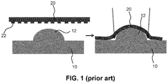
- Fig. 1 schematically depicts a prior art lithographic printing process for printing a surface 10 comprising one or more contours 12.
- a rubber stamp 20 such as a PDMS stamp comprising a pattern of features 22 extending from a planar surface of the stamp 20 is brought into contact with the surface 10 comprising one or more contours 12 and coated with an imprintable layer, e.g. an undeveloped resist layer. This layer is not shown in Fig. 1 .
- the stamp 20 is placed on the surface 10 and deformed by exerting pressure on it such that the stamp 20 assumes the overall shape of the surface 10.
- the resist layer is subsequently developed after which the stamp 20 is removed from the surface 10 to leave behind a developed layer imprinted with the features 22.
- planar stamp 20 can only be deformed by a limited amount, such that the boundary between a contour 12 and the remainder of the surface 10 cannot be contacted by the stamp 20, as indicated by the arrows in the right-hand pane of Fig. 1 (the features 22 are omitted in the right-hand pane for the sake of clarity). Consequently, a partially imprinted article is obtained, in which the pattern of features 22 is absent in these boundary regions.
- the size of the uncovered area can be reduced by increasing the pressure on the stamp 20 during the imprinting process, but this reduces the lifetime of the stamp 20 and increases the risk of deformation of the pattern of features 22 during the imprinting process, which reduces the quality of the transferred pattern on the surface 10.
- a stamp having a patterned surface with an overall shape that complements the surface 10 of the article to be patterned.
- This has the benefit that the stamp surface does not need to be deformed to be brought into contact with the surface 10 including the boundary region of the contour 12. Consequently, the stamp is capable of transferring its pattern of features to the whole of the surface 10 including the boundary regions of the one or more contours 12 on the surface 10.
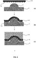
- Fig. 2 schematically depicts the various steps of a method according to an embodiment of the present invention for manufacturing a stamp for use in a soft lithography process, e.g. a nanoscale patterning process of contoured surfaces, as will be explained in more detail later.
- the method commences in step (a) with the provision of a pliable stamp layer 120 carrying a pattern of features 122.
- the stamp layer 120 derives its pliability from the chosen stamp material and its thickness.
- the stamp layer 120 is made of an elastomer or rubber-like material, such as a suitable block-copolymer, e.g. SEBS, or a polysiloxane-based rubber-like material.
- the stamp layer 120 is made of a polysiloxane-based rubber-like material such as PDMS, a T-branched and/or a Q-branched polysiloxane-based rubber-like material as for instance disclosed in WO2009/147602 A2 .
- a T-branched polysiloxane comprises 3-way branching chains, i.e. networks, for instance when crosslinked by linear polysiloxanes.
- a Q- branched polysiloxane comprises 4-way branching chains, i.e. networks, for instance when crosslinked by linear polysiloxanes.
- the stamp layer 120 is made of PDMS. It should however be understood that the stamp layer 120 may be made of any suitably pliable material.
- the pliable stamp layer 120 should have a thickness that allows the stamp layer 120 to be pliable, i.e. to form an intimate contact with the boundary regions of the contours on the surface 10. It will be understood that the suitable thickness of the pliable stamp layer 120 will depend on the material chosen for the pliable stamp layer 120.
- the pliable stamp layer 120 typically will have a thickness of no more than a few mm, e.g. 1 mm or less to ensure that the stamp layer 120 has the desired pliability characteristics.
- the pliable stamp layer 120 may be made of a rubbery material such as PDMS and/or may have a maximum thickness in the range of 100-1,000 micron, although it should be understood that the lower limit of this range may be further reduced, e.g.
- the thickness of the pliable stamp layer 120 is defined as the combination of the thickness of its bulk material and the height of the features 122.
- the features 122 define a pattern to be transferred to a surface 10 comprising at least one contour 12.
- the features 122 may have a feature size ranging from several microns to a few nanometers, i.e. the features 122 may define a nanopattern, although it is also feasible to use larger feature sizes.
- the pliable stamp layer 120 may have a Young's modulus that is tailored to the intended sizes of the features 122 of the stamp to be manufactured. For instance, for relatively large feature sizes, e.g. feature sizes of 500 nm up to several microns, e.g. 2 micron or 5 micron, a relatively soft rubbery material may be used, e.g.
- a rubbery material having a Young's modulus in the range of 2.5-5 MPa such as a soft PDMS.
- a rubbery material having a Young's modulus in the range of 7-11 MPa such as a hard PDMS
- a rubbery material having a Young's modulus in the range of 40-80 MPa such as an extra hard PDMS (sometimes referred to as X-PDMS) may be contemplated.
- the pattern of features 122 may be formed in the pliable stamp layer 120 in any suitable manner. Known techniques such as electron beam etching or interference lithography may be used to form the pattern of features 122.
- the surface 10 comprising at least one contour 12 will also be referred to as the contoured surface 10.
- the contoured surface 10 has a length ranging from a few microns to several cm.
- the stamp layer 120 may have a length matching the length of the contoured surface 120.
- the contoured surface 10 may be of any suitable material, e.g. glass, a suitable polymer, a metal, a semiconductor material such as Si, SiGe, AlGaN, and so on.
- the contoured surface 10 may form part of an article to be mass-produced, such that multiple copies or instances of the contoured surface 10 are to be imprinted.
- the contoured surface 10 as shown in Fig. 2 acts as a template for these multiple copies or instances of the contoured surface 10.
- the pliable stamp layer 120 is applied over the contoured surface 10 such that the pattern of features 122 is brought into contact with the contoured surface 10. Due to its limited thickness, the pliable stamp layer 120 can be brought into contact with the entire surface of the contoured surface 10, including the boundary region of the contours 12, i.e. the region in which the contoured surface 10 may comprise a discontinuity. In an embodiment, the pliable stamp layer 120 is applied over the contoured surface 10 under reduced pressure, as this further improves the intimate relationship between the features 122 and the contoured surface 10. In an alternative embodiment, the pliable stamp layer 120 is applied over the contoured surface 10 whilst applying an overpressure.
- the removal of the air or other gas from between the pliable stamp layer 120 and the contoured surface 10 ensures that the pliable stamp layer 120 adheres to the contoured surface 10, in particular in the aforementioned discontinuous surface regions of the contoured surface 10.
- a reduced pressure may for instance be achieved by placement of the contoured surface 10 and applied pliable stamp layer 120 in a vacuum chamber and applying a vacuum to the contoured surface 10 and applied pliable stamp layer 120. This will be explained in more detail later.
- An overpressure may instead be applied; it is known per se how an overpressure can be applied to a stamp layer on a surface such that this will not be explained in further detail for the sake of brevity.
- the pattern of features 122 may deform during the application of the pliable stamp layer 120 on the contoured surface 10, e.g. when molding or stretching the pliable stamp layer 120 over the contoured surface 10 and/or when a relatively large pressure, e.g. vacuum pressure, is applied to the pliable stamp layer 120.
- a relatively large pressure e.g. vacuum pressure
- Such deformations may typically occur when voids are present in between the features 122, as the (reduced) pressure will remove the medium, e.g. air, from these voids, which can lead to the deformation of the features 122.
- pliable stamp layer 120 comprises a distorted pattern of features 122 such that during the application step (b) in which the patterned pliable stamp layer 120 is forced onto the contoured surface 10, the distorted pattern of features 122 deforms into the intended or desired pattern of features 122.
- the distorted pattern of features 122 may be empirically determined or may be calculated, e.g. using modelling software that can estimate the deformation of such features 122 under the applied pressures.
- this problem is addressed by applying a soft layer such as an undeveloped resist precursor layer or another suitable liquid layer, e.g. an uncured material composition, onto the contoured surface 10, such that the features 122 are pressed into this soft layer during application step (b). More specifically, the medium in the voids in between the features 122 is replaced by the soft layer material, e.g. the resist material, such that the soft layer material in these voids provides structural support to the features 122, thereby preventing significant distortion of the features 122.
- This therefore may obviate the need to provide the patterned pliable stamp layer 120 with a distorted pattern of features 122 as the pattern does not significantly deform during the application step (b). As such, this embodiment may provide a more cost-effective solution to the deformation problem.
- step (c) in which a precursor material 130 for forming a support layer on the pliable stamp layer 120 is deposited on the pliable stamp layer 120.
- step (c) i.e., the deposition of the precursor material 130 on the pliable stamp layer 120 may also be performed under reduced pressure, e.g. by providing a small opening in the vacuum chamber that provides access to the top of the pliable stamp layer 120 for the fluid or liquid precursor material 130 to be poured onto the pliable stamp layer 120 whilst maintaining a reduced pressure in the vacuum chamber to preserve the match between the pliable stamp layer 120 and the contoured surface 10.
- the precursor material 130 typically is a fluid material, e.g.
- the contoured surface 10 and applied pliable stamp layer 120 may be placed in a suitable container to prevent the fluid precursor material 130 from spilling beyond the boundaries of the contoured surface 10.
- the precursor material 130 preferably is a composition for forming a rubber-like support layer on the pliable stamp layer 120.
- the rubber-like support layer preferably has similar or identical thermal expansion coefficients as the pliable stamp layer 120. This may for instance be achieved by the pliable stamp layer 120 and the rubber-like support layer having the same material composition.
- the precursor material 130 is a composition for forming a PDMS having a Young's modulus of 2.5 - 5 MPa, i.e. a soft PDMS.
- the soft PDMS rubber-like support layer may be combined with any of the aforementioned PDMS pliable stamp layers 120, i.e. with a PDMS pliable stamp layer 120 having the same or a higher Young's modulus.
- the thickness of the precursor material layer 130 is such that upon solidification of the precursor material layer 130 to form the rubber-like support layer on the pliable stamp layer 120, the resulting stamp has good structural integrity, such that the surface of the pliable stamp layer 120 carrying the pattern of features 122 does not readily deform.
- the rubber-like support layer fixates the shape of the contoured surface 10 in the surface of the pliable stamp layer 120 carrying the pattern of features 122.
- the precursor material layer 130 is solidified in step (d) to form the rubber-like support layer 140.
- the solidification process may for instance be achieved by a curing process catalyzed by UV radiation, heat, radicals and combinations thereof.
- the solidification step is also performed under reduced pressure, i.e. inside the vacuum chamber.
- the chemical reactions in the precursor material layer 130 may cause the grafting of the rubber-like support layer 140 onto the pliable stamp layer 120, thereby ensuring a strong bond between the rubber-like support layer 140 and the pliable stamp layer 120.
- suitable types of bonding may also be contemplated; e.g.
- an adhesive on the pliable stamp layer 120 may for instance be applied after formation of the rubber-like support layer 140, after which the rubber-like support layer 140 may be temporarily lifted from the pliable stamp layer 120 to apply the adhesive to the pliable stamp layer 120 or to the surface of the rubber-like support layer 140 to be in contact with the pliable stamp layer 120 after which the rubber-like support layer 140 may be placed again on the pliable stamp layer 120.
- the solidification of the precursor material layer 130 may cause some shrinkage of the features 122 of the pliable stamp layer 120, particularly in the height direction, i.e. the direction perpendicular to the contoured surface 10, especially when the solidification process is performed at elevated temperatures. This may be compensated by initially providing the pliable stamp layer 120 with features 122 that have larger than intended dimensions, such that the features 122 shrink to their intended dimensions during the solidification of the precursor material layer 130.
- a rigid carrier 160 may be formed on the support layer 140, as shown in step (e).
- a rigid carrier 160 may be made of any suitable rigid material, e.g. glass.
- the rigid carrier 160 preferably is made of a material that is thermally matched to the material of a substrate to be patterned by the stamp, i.e. has similar or identical thermal expansion coefficients therewith, such that changes in temperature during the imprinting process do not affect the alignment of the stamp with the surface receiving its pattern.
- the support layer 140 may be affixed to the rigid carrier 160 in any suitable manner, e.g. through grafting or through adhesion using an adhesive.
- the precursor material layer 130 is converted into the support layer 140 in the presence of the rigid carrier 160, such that the rigid carrier 160 is directly grafted onto the patterned stamp.
- This for instance aids to prevent deformation, e.g. shrinkage, of the stamp in the X-Y plane, i.e. the major plane of the contoured surface 10. This further improves the robustness and accuracy of a subsequent imprinting process in which the patterned stamp is used.
- the resultant structure may subsequently be released from the contoured surface 10 to yield a patterned stamp 100 having a stamp layer 120 comprising a stamp surface carrying a pattern of features 122, which stamp surface matches the surface profile of the contoured surface 10, wherein the structural integrity of the stamp 100 is provided by the support layer 140 and optionally by the rigid carrier 160.
- the contoured stamp layer 120 comprises a stamp surface that is the inverse of the patterned contoured surface to be formed.
- the patterned stamp 100 has an elastomeric or rubber body including stamp layer 120 that is made of the same material as the support layer 140, e.g. soft PDMS.
- the patterned stamp 100 has a stamp layer 120 that is made of a different material than the support layer 140, e.g. a soft PDMS support layer 140 and a hard PDMS or X-PDMS stamp layer 120 as previously explained.
- the patterned stamp 100 may have an elastomeric or rubber body including a stamp layer 120 of an elastomeric or rubbery material having the same or a higher Young's modulus as the elastomeric or rubbery material of the support layer 140, as previously explained.
- embodiments of the present invention are directed to any patterned stamp 100 that has a contoured printing surface carrying a pattern of features 122, and that is obtainable by embodiments of the stamp manufacturing method of the present invention.
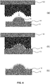
- Fig. 3 schematically depicts a cross-section of an example embodiment of a vacuum chamber 300 in which the patterned pliable stamp layer 120 may be forced onto the contoured surface 10 under reduced pressure as previously explained.
- the vacuum chamber 300 comprises a housing 310 and a lid 312 that may be affixed to the housing 310 in any suitable manner, e.g. using clamps.
- the lid 312 may comprise an opening for exposing the top surface of the pliable stamp layer 120 such that the fluid precursor material 130 can be deposited, e.g. poured, onto the pliable stamp layer 120 as previously explained.
- this opening is sealed by a removable sealing member 313, e.g. a rubber stopper, as is well-known per se.
- a vacuum connector 314 extends through the housing 310 to connect the inner volume 320 of the vacuum chamber 300 to a vacuum pump (not shown). It is noted for the avoidance of doubt that at least in some embodiments the vacuum pump does not form part of the vacuum chamber 300.
- the vacuum chamber 300 may further comprise one or more spacers 322 for carrying a sample holder 324.
- the sample holder 324 may define a liquid container in cooperation with the side walls of the vacuum chamber 300 or may be an integral liquid container in its own right. As previously explained, the sample holder 324 may act as a container for the fluid precursor material 130.
- the patterned pliable stamp layer 120 may extend over the sidewalls of the container and through a recess in the sidewalls of the vacuum chamber 300 into a clamp 326, which clamp 326 may also be connected to the vacuum pump as indicated by arrow 314'.
- a plurality of clamps 326 e.g. a pair of clamps 326 may be provided to secure the patterned pliable stamp layer 120 in the vacuum chamber 300, or on the sample holder 324 to be more precise.
- the portions of the patterned pliable stamp layer 120 that are not intended to contact the contoured surface 10, e.g. the portions of the patterned pliable stamp layer 120 extending over the sidewalls of the liquid container and into the clamps 326, may not carry a pattern of features 122 over the full length of these portions, or may not carry a pattern of features 122 on these portions at all.
- a vacuum may be applied to the vacuum chamber 310 via the vacuum connector 314 such that the patterned pliable stamp layer 120 is sucked onto the contoured surface 10 and onto the sidewalls of the liquid container including the sample holder 324.
- the vacuum is typically applied for a long enough period to ensure an intimate fit between the patterned pliable stamp layer 120 and the contoured surface 10, after which the deposition of the precursor material layer 130 on the pliable stamp layer 120 may take place through the opening in the lid 312, followed by the solidification of the fluid precursor material 130 as previously explained.
- the patterned stamp 100 may additionally comprise sidewalls that are of a different material than the support layer 140.
- the sidewalls are typically of the same material as the patterned pliable stamp layer 120.
- the patterned stamp 100 may for instance comprise a soft PDMS support layer 140 and a hard PDMS or X-PDMS stamp layer 120 and sidewalls as previously explained. More generally, the patterned stamp 100 may have a stamp layer 120 and sidewalls of an elastomeric or rubbery material having the same or a higher Young's modulus as the elastomeric or rubbery material of the support layer 140, as previously explained.
- the stamp 100 may be used in imprinting processes such as soft lithography imprinting processes in which an ink, e.g. a resist layer, on a surface to be patterned is imprinted with a patterned stamp to transfer the stamp pattern into the ink or resist layer. This allows for the formation of patterns having nanoscale feature sizes on such surfaces, as is known per se.
- imprinting processes such as soft lithography imprinting processes in which an ink, e.g. a resist layer, on a surface to be patterned is imprinted with a patterned stamp to transfer the stamp pattern into the ink or resist layer.
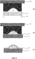
- a receiving surface 10 comprising one or more contours 12 is provided together with an embodiment of the patterned stamp 100 of the present invention.
- An ink or resist precursor layer 14 to be imprinted by the patterned stamp 100 is provided on the contoured surface 10.
- the ink or resist precursor layer 14 may be any suitable material, e.g. an organic or inorganic resist precursor material. As such materials are well-known per se and widely documented, a further description of the compositions of such materials is omitted for the sake of brevity only.
- the material used for the contoured surface 10 is not particularly limited. Any suitable material may be used for the contoured surface as previously explained.
- contoured surface 10 to be imprinted shown in Fig. 4 is identical to the contoured surface 10 shown in Fig. 2 to form the patterned stamp 100, thereby ensuring that the contoured surface of the patterned stamp 100 precisely matches the shape of the contoured surface 10 upon correct alignment, including the boundary regions of the contours 12 as previously explained in more detail.
- step (b) the ink or resist layer 14 is imprinted with the patterned stamp 100 and subsequently developed, e.g. solidified through a curing reaction, to form the patterned ink or resist layer 16 on the contoured surface 10, after which the patterned stamp 100 is removed in step (c) to yield an article comprising a contoured surface 10 carrying a patterned ink or resist layer 16.
- the pattern on the contoured surface 10 is continuous, i.e. also present in the boundary regions of the contours 12, thus providing a contoured surface pattern of high quality.
- the imprinting method of the present invention is not limited to imprinting contoured surfaces only.
- An alternative embodiment is shown in Fig. 5 , in which the patterned stamp 100 is used to form contours on a planar receiving surface 10.
- a relatively thick (viscous) ink or resist precursor layer 14 is applied on the surface 10 in step (a), after which the ink or resist precursor layer 14 is imprinted with the patterned stamp 100 and subsequently developed in step (b) to yield a patterned ink or resist layer 18 after removal of the patterned stamp 100 in step (c).
- the patterned ink or resist layer 18 includes the contours 12 shown in Figs. 2 and 4 , i.e. the contours 12 do not form an integral part of the substrate comprising the planar surface 10 but instead are formed as part of the developed patterned ink or resist layer 18.
- contours 12 forming part of the developed patterned ink or resist layer 18 are more susceptible to shrinkage than when the contours 12 form an integral part of the contoured surface 10.
- more ink or resist material 14 is required in the method of Fig. 5 .
- the patterned stamp 100 must be carefully aligned with the contoured surface 10 to achieve a high-quality transfer of the pattern of features 122 to the contoured surface 10, whereas in the method of Fig. 5 such alignment requirements are much more relaxed since the contoured surface of the patterned stamp 100 does not match the shape of the planar surface 10.
- the imprinting steps (b) in Fig. 4 and 5 may be performed under reduced pressure, e.g. in a vacuum chamber such as the vacuum chamber 300 to further improve the contact between the patterned stamp 100 and the (contoured) surface 10.
- the method as shown in Fig. 4 i.e. the formation of the feature pattern on an already contoured surface may be useful if the contours have relatively large dimensions, e.g. dimensions of 100 microns to several centimetres and beyond.
- the method shown in Fig. 5 may be less suitable to form patterned contoured surfaces with such dimensions as the amount of shrinkage of the contours 12 formed from the resist material 18 may prohibit the accurate reproduction of the desired contoured surface 10.
- the method shown in FIG. 5 can be used to accurately reproduce the desired contoured surfaces because of the modest amount of shrinkage of the contours 12 formed from the resist material 18.
- the size of the contours in the printing surface of patterned stamp 100 is not particularly limited.
- the contours may have dimensions ranging from about 1 micron to dimensions in the centimetre range, e.g. 1 cm or beyond.
- the ratio defined by the dimensions of the contours in the printing surface of patterned stamp 100 divided by the dimensions of the features 122 is not particularly limited and may range from as little as 2 to as much as 1,000,000,000, e.g. from 5 - 100,000,000 or from 50 - 50,000,000.
- nanometer-sized features may be imprinted onto contoured surfaces having contour dimensions of several centimetres up to a metre.
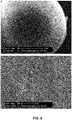
- Fig. 6 shows a pair of SEM images of a glass sphere having a 4 mm diameter that has been imprinted in accordance with the imprinting method of Fig. 4 using a patterned stamp 100 formed in accordance with the method shown in Fig. 2 , in which an identical glass sphere was used as the contoured surface 10.
- the top image shows the resultant structure at 89 x magnification and the bottom image shows the resultant structure at 10,000 x magnification.
- the debris that can be recognized on the glass sphere in the bottom image is contamination of the patterned surface of the glass sphere that is unrelated to the imprinting method.
Description
- The present invention relates to a method of manufacturing a patterned stamp for patterning a contoured surface.
- The present invention further relates to such a patterned stamp.
- The present invention yet further relates to a method of patterning a contoured surface using such a stamp.
- The present invention yet further relates to an article obtained from this patterning method.
- Imprint lithography (IL) is a technique in which a patterned layer such as a masking layer is formed on a substrate such as a semiconductor substrate or as an optical layer by the deposition of a curable imprintable medium. The curable imprintable medium is subsequently patterned by imprinting the medium with a patterned stamp, after which the curable imprintable medium is solidified e.g. when exposed to light, e.g. UV-light to initiate the curing reaction in the medium. After the curing reaction is completed, the stamp is removed from the medium to leave a patterned layer, e.g. on the semiconductor substrate or on a carrier of such an optical layer.
- This technique has recently drawn considerable attention because it can provide a significant cost reduction over traditional lithography process steps. A promising prospect of imprint lithography is that it can be used for forming nanoscale patterns on so-called 2.5D surfaces, i.e. contoured surfaces, which for instance may comprise one or more protrusions, e.g. curved protrusions, emanating from a mainly planar surface. Such techniques may be used to pattern photo-voltaic solar cells, nanowires, VECSEL lasers, medical implants and so on, e.g. by creating nanoscale patterns on optical elements, e.g. lenses or on medical implants, e.g. to stimulate bone or tissue regeneration. To this end, a planar pliable patterned stamp, such as a polysiloxane-based rubber-like stamp, is typically deformed onto the contoured surface such that the stamp pattern is brought into contact with the contoured surface to be patterned. An example of such a stamp is shown in
US 2008/0011934 A1 . - However, a practical problem remains that it is far from trivial to transfer a pattern from a flexible stamp to all of such a contoured surface. In particular, it is difficult to bring the stamp into contact with a boundary region between a planar section and a (curved) protrusion such that such regions can suffer from incomplete or even absent pattern features. This is because it is far from trivial to deform the pliable stamp to such an extent that it exactly matches the contoured surface. In addition, the high pressures required to force the stamp into these boundary regions reduces the lifetime of the stamp and requires more complicated IL device.
- BAHADOR FARSHIAN ET AL: "Soft UV-nanoimprint lithography on non-planar surfaces", MICROELECTRONIC ENGINEERING, ELSEVIER PUBLISHERS BV., AMSTERDAM, NL, vol. 88, no. 11, 20 July 2011 (2011-07-20), pages 3287-3292, and
US 2010/109203 A1 relate to imprinting onto a substrate with a contoured surface. - The present invention seeks to provide a method of manufacturing a patterned stamp for patterning a contoured surface in a more accurate manner.
- The present invention further seeks to provide a patterned stamp for patterning a contoured surface in a more accurate manner.
- The present invention further seeks to provide a method of patterning a contoured surface in a more accurate manner using such a stamp.
- The present invention yet further seeks to provide an article comprising a more accurately patterned contoured surface.
- The invention is defined by the independent claims. The dependent claims provide advantageous embodiments.
- According to an aspect of the invention, there is provided a method of manufacturing a patterned stamp for patterning a contoured surface,
By providing a thin pliable patterned stamp layer over the contoured surface to be patterned, the stamp layer can be brought into contact with every aspect of the contoured surface due to the fact that the bulk support of the stamp that gives the stamp its structural integrity is not yet present. Indeed, this structural integrity limits the pliability of a stamp having a pattern of features extending from a planar surface. Consequently, the absence of the structural integrity provided by the support layer ensures that a good contact between the pattern of features and the contoured surface can be achieved. The subsequent formation of the support layer on the stamp layer fixates the patterned surface of the stamp into a contoured stamp surface carrying a pattern of features that complements the contoured surface to be imprinted, thereby providing a patterned stamp suitable for use in the imprint lithography of such contoured surfaces. - In a preferred embodiment, the step of forcing the pliable stamp layer onto the contoured surface comprises placing the contoured surface with the pliable stamp layer in a vacuum chamber; and reducing the pressure in said vacuum chamber to force the pliable stamp layer onto the contoured surface. This ensures an even more intimate fit between the stamp layer and the contoured surface, thereby further improving the matching of the stamp to the contoured surface. Alternatively, the step of forcing the pliable stamp layer onto the contoured surface may comprise applying an overpressure to the pliable stamp layer to force the pliable stamp layer onto the contoured surface.
- In an embodiment, the solidifying step comprises grafting the support layer onto the pliable stamp layer. This further improves the integration of the stamp layer into the support layer, thereby providing a stamp with excellent structural integrity. This may for instance be achieved if the stamp layer and the support layer comprise a rubbery curable material, such as a polysiloxane-based material. A particularly suitable polysiloxane-based material is polydimethylsiloxane (PDMS). The grafting may for instance take place during the curing of the rubbery material.
- It is recognized that the features of the stamp layer may alter during the manufacturing of the stamp, such that the actual pattern of the stamp may deviate from its intended pattern. Several embodiments of the present method are directed to countering this mismatch.
In an embodiment, the features of the stamp layer have larger than intended dimensions, said features shrinking to the intended dimensions during said solidifying step. - In another embodiment, the method further comprises applying a soft layer onto the contoured surface, wherein the step of forcing the pliable stamp layer onto the contoured surface comprises forcing said features into the soft layer. Consequently, the soft layer provides structural support to the features, i.e. protects the features from deforming under the pressures applied to the stamp layer during the stamp manufacturing process. The soft layer may for instance be a resist layer, which may be undeveloped (i.e. uncured). The soft layer preferably is a liquid layer.
- In yet another embodiment, the pliable stamp layer comprises a distorted pattern of features, and wherein the step of forcing the patterned pliable stamp layer onto the contoured surface comprises deforming the distorted pattern into an intended pattern. It is possible to predict the distortion of the features caused by the pressures applied to the stamp layer during the stamp manufacturing process. By applying the inverse distortion function to the intended pattern, a distorted pattern can be calculated that distorts under said pressures into the intended pattern. In this embodiment, care has to be taken that the deformed pattern is accurately aligned with the contoured surface to ensure that the intended pattern is created in the intended position on the contoured surface.
- The method may further comprise fixating the final patterned stamp on a rigid carrier such as a glass carrier to give further structural integrity to the stamp and reduce the risk of stamp deformation in the X-Y plane (i.e. the plane of the major stamp surface receiving the carrier).
- In accordance with another aspect of the present invention, there is provided a patterned stamp comprising a rubber body including a contoured surface carrying a pattern of relief features that complements a patterned contoured surface to be formed. Such a stamp may be obtained by the stamp manufacturing method of the present invention and provides an excellent fit with a contoured surface to be patterned.
- In an embodiment, the contoured stamp surface carrying the pattern of features is defined by a first layer, the rubber body further comprising a support layer on the first layer, wherein the support layer is of a different material than the first layer. The first layer may be a rubber layer having a first Young's modulus and the support layer is a rubber layer having a second Young's modulus, wherein the first Young's modulus is larger than the second Young's modulus. This has the advantage that a stamp is provided that has excellent overall flexibility combined with an increased robustness against deformation of the features on the contoured surface of the stamp. Also flexibility of the final stamp can be adjusted using the modulus of the support layer, while the first layers modulus can be kept such that good contour coverage is obtained in the stamp manufacturing process.
- The first layer and the second layer may be and preferably are respective PDMS layers.
- In accordance with yet another aspect of the present invention, there is provided a method of forming a patterned contoured surface, This method yields a contoured surface with excellent pattern coverage. The receiving surface may be a contoured surface matching the contours of the stamp surface or may be a planar surface as due to the stamp being contoured, the final patterned surface will also comprise a contoured patterned surface.
- The imprinting step may be performed under reduced pressure, e.g. vacuum, to further improve the contact between the patterned stamp and the contoured surface. There is provided an article comprising a patterned contoured surface obtained by the aforementioned method of forming a patterned contoured surface. Such an article is distinguished from prior art articles by a more complete pattern formation on its contoured surface.
- The invention in all its aspects can be advantageously used in and for imprint lithography where pattern features are of the order of the wavelength of visible light. Due to flexibility of the stamp, the invention is particularly useful for imprint lithography using flexible stamp such as substrate conformal imprint lithography processes when the substrates are moderately or strongly contoured or need contured patterned surfaces (e.g. curved glass that needs a pattern).
- Embodiments of the invention are described in more detail and by way of nonlimiting examples with reference to the accompanying drawings, wherein:
-
Figure 1 schematically depicts a prior art imprinting process; -
Figure 2 schematically depicts a stamp manufacturing method according to an embodiment of the present invention; -
Figure 3 schematically depicts a vacuum chamber for use in the stamp manufacturing method ofFigure 2 ; -
Figure 4 schematically depicts an imprinting method according to an embodiment of the present invention; -
Figure 5 schematically depicts an imprinting method according to another embodiment of the present invention; and -
Figure 6 shows SEM photos of an article imprinted in accordance with the imprinting method ofFigure 4 . - It should be understood that the Figures are merely schematic and are not drawn to scale. It should also be understood that the same reference numerals are used throughout the Figures to indicate the same or similar parts.
-
Fig. 1 schematically depicts a prior art lithographic printing process for printing asurface 10 comprising one ormore contours 12. Arubber stamp 20 such as a PDMS stamp comprising a pattern offeatures 22 extending from a planar surface of thestamp 20 is brought into contact with thesurface 10 comprising one ormore contours 12 and coated with an imprintable layer, e.g. an undeveloped resist layer. This layer is not shown inFig. 1 .Thestamp 20 is placed on thesurface 10 and deformed by exerting pressure on it such that thestamp 20 assumes the overall shape of thesurface 10. The resist layer is subsequently developed after which thestamp 20 is removed from thesurface 10 to leave behind a developed layer imprinted with thefeatures 22. - However, a problem with this approach is that the
planar stamp 20 can only be deformed by a limited amount, such that the boundary between acontour 12 and the remainder of thesurface 10 cannot be contacted by thestamp 20, as indicated by the arrows in the right-hand pane ofFig. 1 (thefeatures 22 are omitted in the right-hand pane for the sake of clarity). Consequently, a partially imprinted article is obtained, in which the pattern offeatures 22 is absent in these boundary regions. The size of the uncovered area can be reduced by increasing the pressure on thestamp 20 during the imprinting process, but this reduces the lifetime of thestamp 20 and increases the risk of deformation of the pattern offeatures 22 during the imprinting process, which reduces the quality of the transferred pattern on thesurface 10. - This problem is addressed by at least some embodiments of the present invention in which a stamp is provided having a patterned surface with an overall shape that complements the
surface 10 of the article to be patterned. This has the benefit that the stamp surface does not need to be deformed to be brought into contact with thesurface 10 including the boundary region of thecontour 12. Consequently, the stamp is capable of transferring its pattern of features to the whole of thesurface 10 including the boundary regions of the one ormore contours 12 on thesurface 10. -
Fig. 2 schematically depicts the various steps of a method according to an embodiment of the present invention for manufacturing a stamp for use in a soft lithography process, e.g. a nanoscale patterning process of contoured surfaces, as will be explained in more detail later. - The method commences in step (a) with the provision of a
pliable stamp layer 120 carrying a pattern offeatures 122. Thestamp layer 120 derives its pliability from the chosen stamp material and its thickness. In an embodiment, thestamp layer 120 is made of an elastomer or rubber-like material, such as a suitable block-copolymer, e.g. SEBS, or a polysiloxane-based rubber-like material. In an embodiment, thestamp layer 120 is made of a polysiloxane-based rubber-like material such as PDMS, a T-branched and/or a Q-branched polysiloxane-based rubber-like material as for instance disclosed inWO2009/147602 A2 . It is noted for the avoidance of doubt that a T-branched polysiloxane comprises 3-way branching chains, i.e. networks, for instance when crosslinked by linear polysiloxanes. Likewise, a Q- branched polysiloxane comprises 4-way branching chains, i.e. networks, for instance when crosslinked by linear polysiloxanes. In yet another embodiment thestamp layer 120 is made of PDMS. It should however be understood that thestamp layer 120 may be made of any suitably pliable material. - The
pliable stamp layer 120 should have a thickness that allows thestamp layer 120 to be pliable, i.e. to form an intimate contact with the boundary regions of the contours on thesurface 10. It will be understood that the suitable thickness of thepliable stamp layer 120 will depend on the material chosen for thepliable stamp layer 120. Thepliable stamp layer 120 typically will have a thickness of no more than a few mm, e.g. 1 mm or less to ensure that thestamp layer 120 has the desired pliability characteristics. In an embodiment, thepliable stamp layer 120 may be made of a rubbery material such as PDMS and/or may have a maximum thickness in the range of 100-1,000 micron, although it should be understood that the lower limit of this range may be further reduced, e.g. to 50 micron, 10 micron or even 1 micron at the cost of increased fragility of thepliable stamp layer 120. For the avoidance of doubt it is clarified that the thickness of thepliable stamp layer 120 is defined as the combination of the thickness of its bulk material and the height of thefeatures 122. - The
features 122 define a pattern to be transferred to asurface 10 comprising at least onecontour 12. Thefeatures 122 may have a feature size ranging from several microns to a few nanometers, i.e. thefeatures 122 may define a nanopattern, although it is also feasible to use larger feature sizes. Thepliable stamp layer 120 may have a Young's modulus that is tailored to the intended sizes of thefeatures 122 of the stamp to be manufactured. For instance, for relatively large feature sizes, e.g. feature sizes of 500 nm up to several microns, e.g. 2 micron or 5 micron, a relatively soft rubbery material may be used, e.g. a rubbery material having a Young's modulus in the range of 2.5-5 MPa, such as a soft PDMS. This is because the relatively largesized features 122 are relatively insensitive to collapse due to surface tension during the stamp manufacturing process or an imprinting process. Such collapse is typically related to the inter-feature distance, with small inter-feature distances causing overlyflexible features 122 to stick together. It is noted that the inter-feature distance is typically but not necessarily correlated to the feature size. - Hence, when smaller sizes of the features 122 (and/or smaller inter-feature distances) are required, more rigid rubbery materials may be contemplated to prevent collapse of the smaller size features 122 due to the aforementioned surface tension. In an embodiment where the dimensions of the stamp features 122 are in the range of 200 nm - 2 micron, a rubbery material having a Young's modulus in the range of 7-11 MPa, such as a hard PDMS may be contemplated, whereas for a stamp having dimensions of the stamp features 122 in the range of 1 nm - 2 micron, a rubbery material having a Young's modulus in the range of 40-80 MPa, such as an extra hard PDMS (sometimes referred to as X-PDMS) may be contemplated. For the avoidance of doubt it is noted that the reported Young's moduli have been determined by a standardized hardness test according to the ASTM D1415 - 06(2012) standard by penetrating the rubber material with a rigid ball under the conditions mandated by the standard.
- The pattern of
features 122 may be formed in thepliable stamp layer 120 in any suitable manner. Known techniques such as electron beam etching or interference lithography may be used to form the pattern offeatures 122. Thesurface 10 comprising at least onecontour 12 will also be referred to as the contouredsurface 10. In an embodiment, the contouredsurface 10 has a length ranging from a few microns to several cm. Thestamp layer 120 may have a length matching the length of the contouredsurface 120. The contouredsurface 10 may be of any suitable material, e.g. glass, a suitable polymer, a metal, a semiconductor material such as Si, SiGe, AlGaN, and so on. The contouredsurface 10 may form part of an article to be mass-produced, such that multiple copies or instances of the contouredsurface 10 are to be imprinted. The contouredsurface 10 as shown inFig. 2 acts as a template for these multiple copies or instances of the contouredsurface 10. - In step (b), the
pliable stamp layer 120 is applied over the contouredsurface 10 such that the pattern offeatures 122 is brought into contact with the contouredsurface 10. Due to its limited thickness, thepliable stamp layer 120 can be brought into contact with the entire surface of the contouredsurface 10, including the boundary region of thecontours 12, i.e. the region in which the contouredsurface 10 may comprise a discontinuity. In an embodiment, thepliable stamp layer 120 is applied over the contouredsurface 10 under reduced pressure, as this further improves the intimate relationship between thefeatures 122 and the contouredsurface 10. In an alternative embodiment, thepliable stamp layer 120 is applied over the contouredsurface 10 whilst applying an overpressure. The removal of the air or other gas from between thepliable stamp layer 120 and the contouredsurface 10 ensures that thepliable stamp layer 120 adheres to the contouredsurface 10, in particular in the aforementioned discontinuous surface regions of the contouredsurface 10. Such a reduced pressure may for instance be achieved by placement of the contouredsurface 10 and appliedpliable stamp layer 120 in a vacuum chamber and applying a vacuum to the contouredsurface 10 and appliedpliable stamp layer 120. This will be explained in more detail later. An overpressure may instead be applied; it is known per se how an overpressure can be applied to a stamp layer on a surface such that this will not be explained in further detail for the sake of brevity. - As previously mentioned, the pattern of
features 122 may deform during the application of thepliable stamp layer 120 on the contouredsurface 10, e.g. when molding or stretching thepliable stamp layer 120 over the contouredsurface 10 and/or when a relatively large pressure, e.g. vacuum pressure, is applied to thepliable stamp layer 120. Such deformations may typically occur when voids are present in between thefeatures 122, as the (reduced) pressure will remove the medium, e.g. air, from these voids, which can lead to the deformation of thefeatures 122. - In an embodiment, this problem is addressed in that
pliable stamp layer 120 comprises a distorted pattern offeatures 122 such that during the application step (b) in which the patternedpliable stamp layer 120 is forced onto the contouredsurface 10, the distorted pattern offeatures 122 deforms into the intended or desired pattern offeatures 122. The distorted pattern offeatures 122 may be empirically determined or may be calculated, e.g. using modelling software that can estimate the deformation ofsuch features 122 under the applied pressures. - In an alternative embodiment, this problem is addressed by applying a soft layer such as an undeveloped resist precursor layer or another suitable liquid layer, e.g. an uncured material composition, onto the contoured
surface 10, such that thefeatures 122 are pressed into this soft layer during application step (b). More specifically, the medium in the voids in between thefeatures 122 is replaced by the soft layer material, e.g. the resist material, such that the soft layer material in these voids provides structural support to thefeatures 122, thereby preventing significant distortion of thefeatures 122. This therefore may obviate the need to provide the patternedpliable stamp layer 120 with a distorted pattern offeatures 122 as the pattern does not significantly deform during the application step (b). As such, this embodiment may provide a more cost-effective solution to the deformation problem. - The method subsequently proceeds to step (c) in which a
precursor material 130 for forming a support layer on thepliable stamp layer 120 is deposited on thepliable stamp layer 120. In case step (b) is performed under reduced pressure, step (c), i.e., the deposition of theprecursor material 130 on thepliable stamp layer 120 may also be performed under reduced pressure, e.g. by providing a small opening in the vacuum chamber that provides access to the top of thepliable stamp layer 120 for the fluid orliquid precursor material 130 to be poured onto thepliable stamp layer 120 whilst maintaining a reduced pressure in the vacuum chamber to preserve the match between thepliable stamp layer 120 and the contouredsurface 10. Theprecursor material 130 typically is a fluid material, e.g. a liquid such as a viscous liquid or gel, such that theprecursor material 130 readily matches the surface profile of thepliable stamp layer 120. Although not specifically shown in step (c), the contouredsurface 10 and appliedpliable stamp layer 120 may be placed in a suitable container to prevent thefluid precursor material 130 from spilling beyond the boundaries of the contouredsurface 10. - The
precursor material 130 preferably is a composition for forming a rubber-like support layer on thepliable stamp layer 120. The rubber-like support layer preferably has similar or identical thermal expansion coefficients as thepliable stamp layer 120. This may for instance be achieved by thepliable stamp layer 120 and the rubber-like support layer having the same material composition. - In an embodiment, the
precursor material 130 is a composition for forming a PDMS having a Young's modulus of 2.5 - 5 MPa, i.e. a soft PDMS. The soft PDMS rubber-like support layer may be combined with any of the aforementioned PDMS pliable stamp layers 120, i.e. with a PDMSpliable stamp layer 120 having the same or a higher Young's modulus. - The thickness of the
precursor material layer 130 is such that upon solidification of theprecursor material layer 130 to form the rubber-like support layer on thepliable stamp layer 120, the resulting stamp has good structural integrity, such that the surface of thepliable stamp layer 120 carrying the pattern offeatures 122 does not readily deform. In other words, the rubber-like support layer fixates the shape of the contouredsurface 10 in the surface of thepliable stamp layer 120 carrying the pattern offeatures 122. - Next, the
precursor material layer 130 is solidified in step (d) to form the rubber-like support layer 140. The solidification process may for instance be achieved by a curing process catalyzed by UV radiation, heat, radicals and combinations thereof. In an embodiment, the solidification step is also performed under reduced pressure, i.e. inside the vacuum chamber. During the solidification process, e.g. through curing, the chemical reactions in theprecursor material layer 130 may cause the grafting of the rubber-like support layer 140 onto thepliable stamp layer 120, thereby ensuring a strong bond between the rubber-like support layer 140 and thepliable stamp layer 120. It will be understood that other suitable types of bonding may also be contemplated; e.g. adhesion by the use of an adhesive on thepliable stamp layer 120, and so on. Such an adhesive may for instance be applied after formation of the rubber-like support layer 140, after which the rubber-like support layer 140 may be temporarily lifted from thepliable stamp layer 120 to apply the adhesive to thepliable stamp layer 120 or to the surface of the rubber-like support layer 140 to be in contact with thepliable stamp layer 120 after which the rubber-like support layer 140 may be placed again on thepliable stamp layer 120. - At this point it is noted that the solidification of the
precursor material layer 130 may cause some shrinkage of thefeatures 122 of thepliable stamp layer 120, particularly in the height direction, i.e. the direction perpendicular to the contouredsurface 10, especially when the solidification process is performed at elevated temperatures. This may be compensated by initially providing thepliable stamp layer 120 withfeatures 122 that have larger than intended dimensions, such that thefeatures 122 shrink to their intended dimensions during the solidification of theprecursor material layer 130. - Upon solidification of the solidification of the
precursor material layer 130 to form thesupport layer 140, arigid carrier 160 may be formed on thesupport layer 140, as shown in step (e). Such arigid carrier 160 may be made of any suitable rigid material, e.g. glass. Therigid carrier 160 preferably is made of a material that is thermally matched to the material of a substrate to be patterned by the stamp, i.e. has similar or identical thermal expansion coefficients therewith, such that changes in temperature during the imprinting process do not affect the alignment of the stamp with the surface receiving its pattern. Thesupport layer 140 may be affixed to therigid carrier 160 in any suitable manner, e.g. through grafting or through adhesion using an adhesive. In an embodiment, theprecursor material layer 130 is converted into thesupport layer 140 in the presence of therigid carrier 160, such that therigid carrier 160 is directly grafted onto the patterned stamp. This for instance aids to prevent deformation, e.g. shrinkage, of the stamp in the X-Y plane, i.e. the major plane of the contouredsurface 10. This further improves the robustness and accuracy of a subsequent imprinting process in which the patterned stamp is used. - The resultant structure may subsequently be released from the contoured
surface 10 to yield a patternedstamp 100 having astamp layer 120 comprising a stamp surface carrying a pattern offeatures 122, which stamp surface matches the surface profile of the contouredsurface 10, wherein the structural integrity of thestamp 100 is provided by thesupport layer 140 and optionally by therigid carrier 160. In other words, the contouredstamp layer 120 comprises a stamp surface that is the inverse of the patterned contoured surface to be formed. - In an embodiment, the patterned
stamp 100 has an elastomeric or rubber body includingstamp layer 120 that is made of the same material as thesupport layer 140, e.g. soft PDMS. In an alternative embodiment, the patternedstamp 100 has astamp layer 120 that is made of a different material than thesupport layer 140, e.g. a softPDMS support layer 140 and a hard PDMS orX-PDMS stamp layer 120 as previously explained. More generally, the patternedstamp 100 may have an elastomeric or rubber body including astamp layer 120 of an elastomeric or rubbery material having the same or a higher Young's modulus as the elastomeric or rubbery material of thesupport layer 140, as previously explained. It should be understood that it is desirable to use a material for thepliable stamp layer 120 with a Young's modulus that is as low as possible to ensure an easy release of the patternedstamp 100 from a layer imprinted by the patternedstamp 100 to maximize the lifetime of the patternedstamp 100. - It is noted for the avoidance of doubt that embodiments of the present invention are directed to any patterned
stamp 100 that has a contoured printing surface carrying a pattern offeatures 122, and that is obtainable by embodiments of the stamp manufacturing method of the present invention. -
Fig. 3 schematically depicts a cross-section of an example embodiment of avacuum chamber 300 in which the patternedpliable stamp layer 120 may be forced onto the contouredsurface 10 under reduced pressure as previously explained. Thevacuum chamber 300 comprises a housing 310 and alid 312 that may be affixed to the housing 310 in any suitable manner, e.g. using clamps. Thelid 312 may comprise an opening for exposing the top surface of thepliable stamp layer 120 such that thefluid precursor material 130 can be deposited, e.g. poured, onto thepliable stamp layer 120 as previously explained. InFig. 3 , this opening is sealed by aremovable sealing member 313, e.g. a rubber stopper, as is well-known per se. Avacuum connector 314 extends through the housing 310 to connect theinner volume 320 of thevacuum chamber 300 to a vacuum pump (not shown). It is noted for the avoidance of doubt that at least in some embodiments the vacuum pump does not form part of thevacuum chamber 300. Thevacuum chamber 300 may further comprise one ormore spacers 322 for carrying asample holder 324. Thesample holder 324 may define a liquid container in cooperation with the side walls of thevacuum chamber 300 or may be an integral liquid container in its own right. As previously explained, thesample holder 324 may act as a container for thefluid precursor material 130. - In an embodiment, the patterned
pliable stamp layer 120 may extend over the sidewalls of the container and through a recess in the sidewalls of thevacuum chamber 300 into aclamp 326, which clamp 326 may also be connected to the vacuum pump as indicated by arrow 314'. A plurality ofclamps 326, e.g. a pair ofclamps 326 may be provided to secure the patternedpliable stamp layer 120 in thevacuum chamber 300, or on thesample holder 324 to be more precise. - In an embodiment, the portions of the patterned
pliable stamp layer 120 that are not intended to contact the contouredsurface 10, e.g. the portions of the patternedpliable stamp layer 120 extending over the sidewalls of the liquid container and into theclamps 326, may not carry a pattern offeatures 122 over the full length of these portions, or may not carry a pattern offeatures 122 on these portions at all. - It should however be understood that alternative embodiments, e.g. an embodiment in which the patterned
pliable stamp layer 120 does not extend over the sidewalls of the liquid container but is intended to contact the contouredsurface 10 only may also be contemplated. - In operation, a vacuum may be applied to the vacuum chamber 310 via the
vacuum connector 314 such that the patternedpliable stamp layer 120 is sucked onto the contouredsurface 10 and onto the sidewalls of the liquid container including thesample holder 324. The vacuum is typically applied for a long enough period to ensure an intimate fit between the patternedpliable stamp layer 120 and the contouredsurface 10, after which the deposition of theprecursor material layer 130 on thepliable stamp layer 120 may take place through the opening in thelid 312, followed by the solidification of thefluid precursor material 130 as previously explained. - It is noted that in case the patterned
stamp 100 is formed in a process in which the patternedpliable stamp layer 120 extends over the sidewalls of the liquid container as shown inFig. 3 , the patternedstamp 100 may additionally comprise sidewalls that are of a different material than thesupport layer 140. The sidewalls are typically of the same material as the patternedpliable stamp layer 120. The patternedstamp 100 may for instance comprise a softPDMS support layer 140 and a hard PDMS orX-PDMS stamp layer 120 and sidewalls as previously explained. More generally, the patternedstamp 100 may have astamp layer 120 and sidewalls of an elastomeric or rubbery material having the same or a higher Young's modulus as the elastomeric or rubbery material of thesupport layer 140, as previously explained. - The
stamp 100 may be used in imprinting processes such as soft lithography imprinting processes in which an ink, e.g. a resist layer, on a surface to be patterned is imprinted with a patterned stamp to transfer the stamp pattern into the ink or resist layer. This allows for the formation of patterns having nanoscale feature sizes on such surfaces, as is known per se. - An example embodiment of an imprinting method in accordance with the present invention is shown in
Fig. 4 . In step (a), a receivingsurface 10 comprising one ormore contours 12 is provided together with an embodiment of the patternedstamp 100 of the present invention. An ink or resistprecursor layer 14 to be imprinted by the patternedstamp 100 is provided on the contouredsurface 10. The ink or resistprecursor layer 14 may be any suitable material, e.g. an organic or inorganic resist precursor material. As such materials are well-known per se and widely documented, a further description of the compositions of such materials is omitted for the sake of brevity only. Similarly, the material used for the contouredsurface 10 is not particularly limited. Any suitable material may be used for the contoured surface as previously explained. It is noted that the contouredsurface 10 to be imprinted shown inFig. 4 is identical to the contouredsurface 10 shown inFig. 2 to form the patternedstamp 100, thereby ensuring that the contoured surface of the patternedstamp 100 precisely matches the shape of the contouredsurface 10 upon correct alignment, including the boundary regions of thecontours 12 as previously explained in more detail. - In step (b), the ink or resist
layer 14 is imprinted with the patternedstamp 100 and subsequently developed, e.g. solidified through a curing reaction, to form the patterned ink or resistlayer 16 on the contouredsurface 10, after which the patternedstamp 100 is removed in step (c) to yield an article comprising a contouredsurface 10 carrying a patterned ink or resistlayer 16. As previously explained, such an article benefits from the fact the pattern on the contouredsurface 10 is continuous, i.e. also present in the boundary regions of thecontours 12, thus providing a contoured surface pattern of high quality. - At this point it is noted that the imprinting method of the present invention is not limited to imprinting contoured surfaces only. An alternative embodiment is shown in
Fig. 5 , in which the patternedstamp 100 is used to form contours on a planar receivingsurface 10. To this end, a relatively thick (viscous) ink or resistprecursor layer 14 is applied on thesurface 10 in step (a), after which the ink or resistprecursor layer 14 is imprinted with the patternedstamp 100 and subsequently developed in step (b) to yield a patterned ink or resistlayer 18 after removal of the patternedstamp 100 in step (c). The patterned ink or resistlayer 18 includes thecontours 12 shown inFigs. 2 and4 , i.e. thecontours 12 do not form an integral part of the substrate comprising theplanar surface 10 but instead are formed as part of the developed patterned ink or resistlayer 18. - It is noted that the
contours 12 forming part of the developed patterned ink or resistlayer 18 are more susceptible to shrinkage than when thecontours 12 form an integral part of the contouredsurface 10. Also, it will be apparent that more ink or resistmaterial 14 is required in the method ofFig. 5 . However, in the imprinting method ofFig. 4 , the patternedstamp 100 must be carefully aligned with the contouredsurface 10 to achieve a high-quality transfer of the pattern offeatures 122 to the contouredsurface 10, whereas in the method ofFig. 5 such alignment requirements are much more relaxed since the contoured surface of the patternedstamp 100 does not match the shape of theplanar surface 10. - At this point, it is noted that the imprinting steps (b) in
Fig. 4 and5 may be performed under reduced pressure, e.g. in a vacuum chamber such as thevacuum chamber 300 to further improve the contact between the patternedstamp 100 and the (contoured)surface 10. - The method as shown in
Fig. 4 , i.e. the formation of the feature pattern on an already contoured surface may be useful if the contours have relatively large dimensions, e.g. dimensions of 100 microns to several centimetres and beyond. The method shown inFig. 5 may be less suitable to form patterned contoured surfaces with such dimensions as the amount of shrinkage of thecontours 12 formed from the resistmaterial 18 may prohibit the accurate reproduction of the desired contouredsurface 10. However, for smaller contour sizes, e.g. contour sizes in the range of 1-100 micron, the method shown inFIG. 5 can be used to accurately reproduce the desired contoured surfaces because of the modest amount of shrinkage of thecontours 12 formed from the resistmaterial 18. - At this point, it is noted that the size of the contours in the printing surface of patterned
stamp 100 is not particularly limited. The contours may have dimensions ranging from about 1 micron to dimensions in the centimetre range, e.g. 1 cm or beyond. Moreover, the ratio defined by the dimensions of the contours in the printing surface of patternedstamp 100 divided by the dimensions of thefeatures 122 is not particularly limited and may range from as little as 2 to as much as 1,000,000,000, e.g. from 5 - 100,000,000 or from 50 - 50,000,000. In other words, nanometer-sized features may be imprinted onto contoured surfaces having contour dimensions of several centimetres up to a metre. -
Fig. 6 shows a pair of SEM images of a glass sphere having a 4 mm diameter that has been imprinted in accordance with the imprinting method ofFig. 4 using a patternedstamp 100 formed in accordance with the method shown inFig. 2 , in which an identical glass sphere was used as the contouredsurface 10. The top image shows the resultant structure at 89 x magnification and the bottom image shows the resultant structure at 10,000 x magnification. It can be readily recognized inFig. 6 that a regular pattern has been produced on the glass sphere with negligible defects. The debris that can be recognized on the glass sphere in the bottom image is contamination of the patterned surface of the glass sphere that is unrelated to the imprinting method. - It should be noted that the above-mentioned embodiments illustrate rather than limit the invention, and that those skilled in the art will be able to design many alternative embodiments without departing from the scope of the appended claims. In the claims, any reference signs placed between parentheses shall not be construed as limiting the claim. The word "comprising" does not exclude the presence of elements or steps other than those listed in a claim. The word "a" or "an" preceding an element does not exclude the presence of a plurality of such elements.
Claims (13)
- A method of manufacturing a patterned stamp (100) for patterning a contoured surface (10), the method comprising:providing a pliable stamp layer (120) carrying a pattern of relief features (122);forcing the pliable stamp layer onto the contoured surface with said pattern of relief features facing the contoured surface;applying a fluid support layer (130) over the pliable stamp layer on the contoured surface;solidifying the support layer (140) to form the patterned stamp; andremoving the patterned stamp from the contoured surface.
- The method of claim 1, wherein the step of forcing the pliable stamp layer (120) onto the contoured surface (10) comprises:placing the contoured surface with the pliable stamp layer in a vacuum chamber (300); andreducing the pressure in said vacuum chamber to force the pliable stamp layer onto the contoured surface.
- The method of claim 1 or 2, wherein said solidifying step comprises grafting the support layer (140) onto the pliable stamp layer (120).
- The method of claim 3, wherein the pliable stamp layer (120) and the support layer (140) comprise a rubbery material.
- The method of claim 4, wherein the rubbery material is a siloxane-based material such as polydimethylsiloxane.
- The method of any of claims 1-5, wherein said features (122) have a larger than intended dimensions, said features shrinking to the intended dimensions during said solidifying step.
- The method of any of claims 1-6, further comprising applying a soft layer such as a liquid layer onto the contoured surface (10), wherein the step of forcing the pliable stamp layer (120) onto the contoured surface comprises forcing said features (122) into the soft layer.
- The method of any of claims 1-7, wherein the pliable stamp layer (120) comprises a distorted pattern of features (122), and wherein the step of forcing the patterned pliable stamp layer onto the contoured surface (10) comprises deforming the distorted pattern into an intended pattern.
- The method of any of claims 1-8, further comprising fixating the patterned stamp (100) on a rigid carrier (160).
- A patterned stamp (100) for use in an imprint lithography process, the patterned stamp comprising a rubber body comprising a contoured stamp surface (120) carrying a pattern of relief features (122), wherein the rubber body includes a support layer (140) and a first layer supported by the support layer, the first layer comprising the contoured stamp surface carrying the pattern of relief features, wherein the support layer is of a different material than the first layer, wherein the first layer (120) is a rubber layer having a first Young's modulus and the support layer (140) is a rubber layer having a second Young's modulus, wherein the first Young's modulus is larger than the second Young's modulus.
- The patterned stamp of claim 10, wherein the first layer and the second layer are respective PDMS layers.
- An imprint lithography method of forming a patterned contoured surface (10) on a receiving surface, the method comprising:providing a pattern precursor layer (14) over the receiving surface (10);imprinting the pattern precursor layer with a patterned stamp (100) according to claim 10 or 11;developing the pattern precursor layer into a pattern layer (16, 18); andremoving the patterned stamp from the developed pattern layer.
- The use of the patterned stamp of claim 10 or 11 for imprint lithography.
Priority Applications (1)
| Application Number | Priority Date | Filing Date | Title |
|---|---|---|---|
| EP14744033.3A EP3025195B1 (en) | 2013-07-22 | 2014-07-22 | Patterned stamp manufacturing method, patterned stamp and patterned stamp imprinting method |
Applications Claiming Priority (3)
| Application Number | Priority Date | Filing Date | Title |
|---|---|---|---|
| EP13177413 | 2013-07-22 | ||
| PCT/EP2014/065656 WO2015011110A1 (en) | 2013-07-22 | 2014-07-22 | Patterned stamp manufacturing method, patterned stamp imprinting method and imprinted article |
| EP14744033.3A EP3025195B1 (en) | 2013-07-22 | 2014-07-22 | Patterned stamp manufacturing method, patterned stamp and patterned stamp imprinting method |
Publications (2)
| Publication Number | Publication Date |
|---|---|
| EP3025195A1 EP3025195A1 (en) | 2016-06-01 |
| EP3025195B1 true EP3025195B1 (en) | 2019-04-24 |
Family
ID=48906098
Family Applications (1)
| Application Number | Title | Priority Date | Filing Date |
|---|---|---|---|
| EP14744033.3A Active EP3025195B1 (en) | 2013-07-22 | 2014-07-22 | Patterned stamp manufacturing method, patterned stamp and patterned stamp imprinting method |
Country Status (9)
| Country | Link |
|---|---|
| US (2) | US9908358B2 (en) |
| EP (1) | EP3025195B1 (en) |
| JP (1) | JP6356798B2 (en) |
| KR (1) | KR102209564B1 (en) |
| CN (1) | CN105378563B (en) |
| RU (1) | RU2671324C2 (en) |
| TR (1) | TR201909168T4 (en) |
| TW (1) | TWI665078B (en) |
| WO (1) | WO2015011110A1 (en) |
Families Citing this family (6)
| Publication number | Priority date | Publication date | Assignee | Title |
|---|---|---|---|---|
| US11086217B2 (en) | 2014-12-22 | 2021-08-10 | Koninklijke Philips N.V. | Patterned stamp manufacturing method, patterned stamp and imprinting method |
| JP6565321B2 (en) * | 2015-05-18 | 2019-08-28 | 凸版印刷株式会社 | Laminated structure, organic EL element using the same, and manufacturing method thereof |
| CN109600996B (en) * | 2016-07-27 | 2021-11-30 | 皇家飞利浦有限公司 | Polyorganosiloxane-based stamp, method for the production thereof, use thereof for a printing process, and imprint method using same |
| US10035296B2 (en) * | 2016-10-13 | 2018-07-31 | Canon Kabushiki Kaisha | Methods for controlling spread of imprint material |
| CN106626831B (en) * | 2016-12-28 | 2022-12-27 | 临沂市名涛新型材料有限公司 | Printing device used on spherical surface or arc-shaped concave surface and application thereof |
| CN114450141A (en) * | 2019-08-07 | 2022-05-06 | 恩图鲁斯特有限公司 | Ink ribbon imprinter/indenter for plastic cards |
Family Cites Families (21)
| Publication number | Priority date | Publication date | Assignee | Title |
|---|---|---|---|---|
| US2994266A (en) | 1959-03-09 | 1961-08-01 | American Optical Corp | Hand stamps |
| SU889468A1 (en) * | 1980-04-07 | 1981-12-15 | Всесоюзный Научно-Исследовательский Институт Резинотехничнского Машиностроения | Press mould for vulcanizing rubber-cord envelopes |
| JPH05200757A (en) * | 1992-01-30 | 1993-08-10 | Canon Inc | Flexible stamper, roll-shaped stamper and production of substrate for optical data recording medium |
| JP3482115B2 (en) * | 1997-10-13 | 2003-12-22 | 東レ・ダウコーニング・シリコーン株式会社 | Curable silicone composition and electronic component |
| DE19819463B4 (en) * | 1998-04-30 | 2004-03-25 | Siemens Ag | Powertrain control of a motor vehicle |
| GB9811634D0 (en) * | 1998-05-29 | 1998-07-29 | Unilever Plc | Stamping dies |
| JP3941604B2 (en) | 2002-06-26 | 2007-07-04 | 富士ゼロックス株式会社 | Microlens array manufacturing method, electrolytic solution and microlens array resin material used therefor, and master manufacturing apparatus |
| CN101427182B (en) | 2004-04-27 | 2011-10-19 | 伊利诺伊大学评议会 | Composite patterning devices for soft lithography |
| EP1789848B1 (en) | 2004-09-08 | 2010-06-30 | NIL Technology APS | A flexible nano-imprint stamp |
| KR20070106683A (en) * | 2004-09-08 | 2007-11-05 | 닐 테크놀로지 에이피에스 | A flexible nano-imprint stamp |
| US20060144262A1 (en) * | 2005-01-03 | 2006-07-06 | Ji-Sung Koong | Marking apparatus for golf ball and stamp for thereof |
| CN2822970Y (en) * | 2005-09-28 | 2006-10-04 | 蔡碧云 | Seal for fingernail decoration |
| US8318253B2 (en) | 2006-06-30 | 2012-11-27 | Asml Netherlands B.V. | Imprint lithography |
| US7678423B2 (en) * | 2007-02-27 | 2010-03-16 | The Regents Of The University Of Michigan | System and method for depositing thin layers on non-planar substrates by stamping |
| JP4448868B2 (en) * | 2007-06-29 | 2010-04-14 | 株式会社日立産機システム | Imprint stamper and manufacturing method thereof |
| WO2009014717A1 (en) * | 2007-07-25 | 2009-01-29 | Nano Terra Inc. | Contact printing method using an elastomeric stamp having a variable surface area and variable shape |
| CN101221358A (en) * | 2008-02-04 | 2008-07-16 | 哈尔滨工业大学 | Curved substrate multi-phase micro-optical element processing method based on flexible ultraviolet die mold |
| RU2497850C2 (en) * | 2008-06-06 | 2013-11-10 | Конинклейке Филипс Электроникс Н.В. | Silicone rubber material for soft lithography |
| CN101477304B (en) * | 2008-11-04 | 2011-08-17 | 南京大学 | Stamping method for copying high-resolution nano-structure on complicated shape surface |
| JP2011062978A (en) * | 2009-09-18 | 2011-03-31 | Fujifilm Corp | Peeling plate used for imprinting method, mold structure and imprinting method |
| JP2013004669A (en) * | 2011-06-15 | 2013-01-07 | Toshiba Corp | Pattern formation method, electronic device manufacturing method and electronic device |
-
2014
- 2014-07-21 TW TW103124966A patent/TWI665078B/en active
- 2014-07-22 TR TR2019/09168T patent/TR201909168T4/en unknown
- 2014-07-22 RU RU2016105665A patent/RU2671324C2/en active
- 2014-07-22 JP JP2016528491A patent/JP6356798B2/en active Active
- 2014-07-22 WO PCT/EP2014/065656 patent/WO2015011110A1/en active Application Filing
- 2014-07-22 EP EP14744033.3A patent/EP3025195B1/en active Active
- 2014-07-22 CN CN201480041800.6A patent/CN105378563B/en active Active
- 2014-07-22 US US14/905,856 patent/US9908358B2/en active Active
- 2014-07-22 KR KR1020167004296A patent/KR102209564B1/en active IP Right Grant
-
2018
- 2018-01-18 US US15/874,068 patent/US11453232B2/en active Active
Non-Patent Citations (1)
| Title |
|---|
| None * |
Also Published As
| Publication number | Publication date |
|---|---|
| TWI665078B (en) | 2019-07-11 |
| TW201518067A (en) | 2015-05-16 |
| WO2015011110A1 (en) | 2015-01-29 |
| US11453232B2 (en) | 2022-09-27 |
| US20160152064A1 (en) | 2016-06-02 |
| RU2016105665A (en) | 2017-08-29 |
| EP3025195A1 (en) | 2016-06-01 |
| KR102209564B1 (en) | 2021-02-02 |
| JP2016527720A (en) | 2016-09-08 |
| KR20160034363A (en) | 2016-03-29 |
| US20180141366A1 (en) | 2018-05-24 |
| RU2016105665A3 (en) | 2018-05-08 |
| CN105378563A (en) | 2016-03-02 |
| TR201909168T4 (en) | 2019-07-22 |
| CN105378563B (en) | 2020-07-14 |
| US9908358B2 (en) | 2018-03-06 |
| RU2671324C2 (en) | 2018-10-30 |
| JP6356798B2 (en) | 2018-07-11 |
Similar Documents
| Publication | Publication Date | Title |
|---|---|---|
| US11453232B2 (en) | Patterned stamp manufacturing method, patterned stamp imprinting method and imprinted article | |
| RU2695290C2 (en) | Method of making die with pattern, die with pattern and method for printing | |
| CN1890604B (en) | Device and method for large area lithography | |
| US20100018420A1 (en) | Reinforced Composite Stamp for Dry Transfer Printing of Semiconductor Elements | |
| CN101036086A (en) | A flexible nano-imprint stamp | |
| TWI576229B (en) | Safe separation for nano imprinting | |
| KR20090077836A (en) | Devices and methods for pattern generation by ink lithography | |
| CN1659691A (en) | Replication and transfer of microstructures and nanostructures | |
| JP2009190300A (en) | Imprint device and imprint method | |
| JP5282510B2 (en) | Manufacturing method of stamp for micro contact printing (μCP) | |
| KR100922574B1 (en) | Apparatus for fixing plastic sheet and Fabrication method of nanopattern on plastic sheet using this same | |
| CN100594137C (en) | Pattern forming method and device | |
| TWI654134B (en) | Method and device for embossing a nano structure | |
| US20210268693A1 (en) | A nanocomposite mold for thermal nanoimprinting and method for producing the same | |
| CN112526660A (en) | Method for manufacturing nano-grating on curved surface, optical device and electronic equipment | |
| KR101551772B1 (en) | Replica stamp for SCIL process and manufacturing method for thereof | |
| KR20230034942A (en) | Apparatus and method for manufacturing micro and/or nano structures |
Legal Events
| Date | Code | Title | Description |
|---|---|---|---|
| PUAI | Public reference made under article 153(3) epc to a published international application that has entered the european phase |
Free format text: ORIGINAL CODE: 0009012 |
|
| 17P | Request for examination filed |
Effective date: 20160222 |
|
| AK | Designated contracting states |
Kind code of ref document: A1 Designated state(s): AL AT BE BG CH CY CZ DE DK EE ES FI FR GB GR HR HU IE IS IT LI LT LU LV MC MK MT NL NO PL PT RO RS SE SI SK SM TR |
|
| AX | Request for extension of the european patent |
Extension state: BA ME |
|
| DAX | Request for extension of the european patent (deleted) | ||
| GRAP | Despatch of communication of intention to grant a patent |
Free format text: ORIGINAL CODE: EPIDOSNIGR1 |
|
| STAA | Information on the status of an ep patent application or granted ep patent |
Free format text: STATUS: GRANT OF PATENT IS INTENDED |
|
| INTG | Intention to grant announced |
Effective date: 20181114 |
|
| GRAS | Grant fee paid |
Free format text: ORIGINAL CODE: EPIDOSNIGR3 |
|
| GRAA | (expected) grant |
Free format text: ORIGINAL CODE: 0009210 |
|
| STAA | Information on the status of an ep patent application or granted ep patent |
Free format text: STATUS: THE PATENT HAS BEEN GRANTED |
|
| AK | Designated contracting states |
Kind code of ref document: B1 Designated state(s): AL AT BE BG CH CY CZ DE DK EE ES FI FR GB GR HR HU IE IS IT LI LT LU LV MC MK MT NL NO PL PT RO RS SE SI SK SM TR |
|
| REG | Reference to a national code |
Ref country code: GB Ref legal event code: FG4D |
|
| REG | Reference to a national code |
Ref country code: CH Ref legal event code: EP |
|
| REG | Reference to a national code |
Ref country code: AT Ref legal event code: REF Ref document number: 1124828 Country of ref document: AT Kind code of ref document: T Effective date: 20190515 Ref country code: IE Ref legal event code: FG4D |
|
| REG | Reference to a national code |
Ref country code: DE Ref legal event code: R096 Ref document number: 602014045348 Country of ref document: DE |
|
| REG | Reference to a national code |
Ref country code: NL Ref legal event code: MP Effective date: 20190424 |
|
| REG | Reference to a national code |
Ref country code: LT Ref legal event code: MG4D |
|
| PG25 | Lapsed in a contracting state [announced via postgrant information from national office to epo] |
Ref country code: NL Free format text: LAPSE BECAUSE OF FAILURE TO SUBMIT A TRANSLATION OF THE DESCRIPTION OR TO PAY THE FEE WITHIN THE PRESCRIBED TIME-LIMIT Effective date: 20190424 |
|
| PG25 | Lapsed in a contracting state [announced via postgrant information from national office to epo] |
Ref country code: LT Free format text: LAPSE BECAUSE OF FAILURE TO SUBMIT A TRANSLATION OF THE DESCRIPTION OR TO PAY THE FEE WITHIN THE PRESCRIBED TIME-LIMIT Effective date: 20190424 Ref country code: FI Free format text: LAPSE BECAUSE OF FAILURE TO SUBMIT A TRANSLATION OF THE DESCRIPTION OR TO PAY THE FEE WITHIN THE PRESCRIBED TIME-LIMIT Effective date: 20190424 Ref country code: SE Free format text: LAPSE BECAUSE OF FAILURE TO SUBMIT A TRANSLATION OF THE DESCRIPTION OR TO PAY THE FEE WITHIN THE PRESCRIBED TIME-LIMIT Effective date: 20190424 Ref country code: PT Free format text: LAPSE BECAUSE OF FAILURE TO SUBMIT A TRANSLATION OF THE DESCRIPTION OR TO PAY THE FEE WITHIN THE PRESCRIBED TIME-LIMIT Effective date: 20190824 Ref country code: NO Free format text: LAPSE BECAUSE OF FAILURE TO SUBMIT A TRANSLATION OF THE DESCRIPTION OR TO PAY THE FEE WITHIN THE PRESCRIBED TIME-LIMIT Effective date: 20190724 Ref country code: HR Free format text: LAPSE BECAUSE OF FAILURE TO SUBMIT A TRANSLATION OF THE DESCRIPTION OR TO PAY THE FEE WITHIN THE PRESCRIBED TIME-LIMIT Effective date: 20190424 Ref country code: AL Free format text: LAPSE BECAUSE OF FAILURE TO SUBMIT A TRANSLATION OF THE DESCRIPTION OR TO PAY THE FEE WITHIN THE PRESCRIBED TIME-LIMIT Effective date: 20190424 Ref country code: ES Free format text: LAPSE BECAUSE OF FAILURE TO SUBMIT A TRANSLATION OF THE DESCRIPTION OR TO PAY THE FEE WITHIN THE PRESCRIBED TIME-LIMIT Effective date: 20190424 |
|
| PG25 | Lapsed in a contracting state [announced via postgrant information from national office to epo] |
Ref country code: GR Free format text: LAPSE BECAUSE OF FAILURE TO SUBMIT A TRANSLATION OF THE DESCRIPTION OR TO PAY THE FEE WITHIN THE PRESCRIBED TIME-LIMIT Effective date: 20190725 Ref country code: RS Free format text: LAPSE BECAUSE OF FAILURE TO SUBMIT A TRANSLATION OF THE DESCRIPTION OR TO PAY THE FEE WITHIN THE PRESCRIBED TIME-LIMIT Effective date: 20190424 Ref country code: BG Free format text: LAPSE BECAUSE OF FAILURE TO SUBMIT A TRANSLATION OF THE DESCRIPTION OR TO PAY THE FEE WITHIN THE PRESCRIBED TIME-LIMIT Effective date: 20190724 Ref country code: LV Free format text: LAPSE BECAUSE OF FAILURE TO SUBMIT A TRANSLATION OF THE DESCRIPTION OR TO PAY THE FEE WITHIN THE PRESCRIBED TIME-LIMIT Effective date: 20190424 Ref country code: PL Free format text: LAPSE BECAUSE OF FAILURE TO SUBMIT A TRANSLATION OF THE DESCRIPTION OR TO PAY THE FEE WITHIN THE PRESCRIBED TIME-LIMIT Effective date: 20190424 |
|
| REG | Reference to a national code |
Ref country code: AT Ref legal event code: MK05 Ref document number: 1124828 Country of ref document: AT Kind code of ref document: T Effective date: 20190424 |
|
| PG25 | Lapsed in a contracting state [announced via postgrant information from national office to epo] |
Ref country code: IS Free format text: LAPSE BECAUSE OF FAILURE TO SUBMIT A TRANSLATION OF THE DESCRIPTION OR TO PAY THE FEE WITHIN THE PRESCRIBED TIME-LIMIT Effective date: 20190824 |
|
| REG | Reference to a national code |
Ref country code: DE Ref legal event code: R097 Ref document number: 602014045348 Country of ref document: DE |
|
| PG25 | Lapsed in a contracting state [announced via postgrant information from national office to epo] |
Ref country code: EE Free format text: LAPSE BECAUSE OF FAILURE TO SUBMIT A TRANSLATION OF THE DESCRIPTION OR TO PAY THE FEE WITHIN THE PRESCRIBED TIME-LIMIT Effective date: 20190424 Ref country code: DK Free format text: LAPSE BECAUSE OF FAILURE TO SUBMIT A TRANSLATION OF THE DESCRIPTION OR TO PAY THE FEE WITHIN THE PRESCRIBED TIME-LIMIT Effective date: 20190424 Ref country code: SK Free format text: LAPSE BECAUSE OF FAILURE TO SUBMIT A TRANSLATION OF THE DESCRIPTION OR TO PAY THE FEE WITHIN THE PRESCRIBED TIME-LIMIT Effective date: 20190424 Ref country code: AT Free format text: LAPSE BECAUSE OF FAILURE TO SUBMIT A TRANSLATION OF THE DESCRIPTION OR TO PAY THE FEE WITHIN THE PRESCRIBED TIME-LIMIT Effective date: 20190424 Ref country code: CZ Free format text: LAPSE BECAUSE OF FAILURE TO SUBMIT A TRANSLATION OF THE DESCRIPTION OR TO PAY THE FEE WITHIN THE PRESCRIBED TIME-LIMIT Effective date: 20190424 Ref country code: RO Free format text: LAPSE BECAUSE OF FAILURE TO SUBMIT A TRANSLATION OF THE DESCRIPTION OR TO PAY THE FEE WITHIN THE PRESCRIBED TIME-LIMIT Effective date: 20190424 |
|
| PG25 | Lapsed in a contracting state [announced via postgrant information from national office to epo] |
Ref country code: SM Free format text: LAPSE BECAUSE OF FAILURE TO SUBMIT A TRANSLATION OF THE DESCRIPTION OR TO PAY THE FEE WITHIN THE PRESCRIBED TIME-LIMIT Effective date: 20190424 Ref country code: MC Free format text: LAPSE BECAUSE OF FAILURE TO SUBMIT A TRANSLATION OF THE DESCRIPTION OR TO PAY THE FEE WITHIN THE PRESCRIBED TIME-LIMIT Effective date: 20190424 Ref country code: IT Free format text: LAPSE BECAUSE OF FAILURE TO SUBMIT A TRANSLATION OF THE DESCRIPTION OR TO PAY THE FEE WITHIN THE PRESCRIBED TIME-LIMIT Effective date: 20190424 |
|
| PLBE | No opposition filed within time limit |
Free format text: ORIGINAL CODE: 0009261 |
|
| REG | Reference to a national code |
Ref country code: CH Ref legal event code: PL |
|
| STAA | Information on the status of an ep patent application or granted ep patent |
Free format text: STATUS: NO OPPOSITION FILED WITHIN TIME LIMIT |
|
| RAP2 | Party data changed (patent owner data changed or rights of a patent transferred) |
Owner name: KONINKLIJKE PHILIPS N.V. |
|
| 26N | No opposition filed |
Effective date: 20200127 |
|
| REG | Reference to a national code |
Ref country code: BE Ref legal event code: MM Effective date: 20190731 |
|
| PG25 | Lapsed in a contracting state [announced via postgrant information from national office to epo] |
Ref country code: BE Free format text: LAPSE BECAUSE OF NON-PAYMENT OF DUE FEES Effective date: 20190731 Ref country code: CH Free format text: LAPSE BECAUSE OF NON-PAYMENT OF DUE FEES Effective date: 20190731 Ref country code: LI Free format text: LAPSE BECAUSE OF NON-PAYMENT OF DUE FEES Effective date: 20190731 Ref country code: SI Free format text: LAPSE BECAUSE OF FAILURE TO SUBMIT A TRANSLATION OF THE DESCRIPTION OR TO PAY THE FEE WITHIN THE PRESCRIBED TIME-LIMIT Effective date: 20190424 Ref country code: LU Free format text: LAPSE BECAUSE OF NON-PAYMENT OF DUE FEES Effective date: 20190722 |
|
| PG25 | Lapsed in a contracting state [announced via postgrant information from national office to epo] |
Ref country code: IE Free format text: LAPSE BECAUSE OF NON-PAYMENT OF DUE FEES Effective date: 20190722 |
|
| PG25 | Lapsed in a contracting state [announced via postgrant information from national office to epo] |
Ref country code: CY Free format text: LAPSE BECAUSE OF FAILURE TO SUBMIT A TRANSLATION OF THE DESCRIPTION OR TO PAY THE FEE WITHIN THE PRESCRIBED TIME-LIMIT Effective date: 20190424 |
|
| PG25 | Lapsed in a contracting state [announced via postgrant information from national office to epo] |
Ref country code: MT Free format text: LAPSE BECAUSE OF FAILURE TO SUBMIT A TRANSLATION OF THE DESCRIPTION OR TO PAY THE FEE WITHIN THE PRESCRIBED TIME-LIMIT Effective date: 20190424 Ref country code: HU Free format text: LAPSE BECAUSE OF FAILURE TO SUBMIT A TRANSLATION OF THE DESCRIPTION OR TO PAY THE FEE WITHIN THE PRESCRIBED TIME-LIMIT; INVALID AB INITIO Effective date: 20140722 |
|
| PG25 | Lapsed in a contracting state [announced via postgrant information from national office to epo] |
Ref country code: MK Free format text: LAPSE BECAUSE OF FAILURE TO SUBMIT A TRANSLATION OF THE DESCRIPTION OR TO PAY THE FEE WITHIN THE PRESCRIBED TIME-LIMIT Effective date: 20190424 |
|
| PGFP | Annual fee paid to national office [announced via postgrant information from national office to epo] |
Ref country code: TR Payment date: 20230711 Year of fee payment: 10 Ref country code: GB Payment date: 20230725 Year of fee payment: 10 |
|
| PGFP | Annual fee paid to national office [announced via postgrant information from national office to epo] |
Ref country code: FR Payment date: 20230725 Year of fee payment: 10 Ref country code: DE Payment date: 20230726 Year of fee payment: 10 |