EP3021189B1 - Spannungsreferenzquelle und Verfahren zur Erzeugung einer Referenzspannung - Google Patents
Spannungsreferenzquelle und Verfahren zur Erzeugung einer Referenzspannung Download PDFInfo
- Publication number
- EP3021189B1 EP3021189B1 EP14193251.7A EP14193251A EP3021189B1 EP 3021189 B1 EP3021189 B1 EP 3021189B1 EP 14193251 A EP14193251 A EP 14193251A EP 3021189 B1 EP3021189 B1 EP 3021189B1
- Authority
- EP
- European Patent Office
- Prior art keywords
- terminal
- transistor
- source
- current
- mirror
- Prior art date
- Legal status (The legal status is an assumption and is not a legal conclusion. Google has not performed a legal analysis and makes no representation as to the accuracy of the status listed.)
- Active
Links
Images


Classifications
-
- G—PHYSICS
- G05—CONTROLLING; REGULATING
- G05F—SYSTEMS FOR REGULATING ELECTRIC OR MAGNETIC VARIABLES
- G05F3/00—Non-retroactive systems for regulating electric variables by using an uncontrolled element, or an uncontrolled combination of elements, such element or such combination having self-regulating properties
- G05F3/02—Regulating voltage or current
- G05F3/08—Regulating voltage or current wherein the variable is DC
- G05F3/10—Regulating voltage or current wherein the variable is DC using uncontrolled devices with non-linear characteristics
- G05F3/16—Regulating voltage or current wherein the variable is DC using uncontrolled devices with non-linear characteristics being semiconductor devices
- G05F3/20—Regulating voltage or current wherein the variable is DC using uncontrolled devices with non-linear characteristics being semiconductor devices using diode- transistor combinations
- G05F3/26—Current mirrors
- G05F3/267—Current mirrors using both bipolar and field-effect technology
-
- G—PHYSICS
- G05—CONTROLLING; REGULATING
- G05F—SYSTEMS FOR REGULATING ELECTRIC OR MAGNETIC VARIABLES
- G05F3/00—Non-retroactive systems for regulating electric variables by using an uncontrolled element, or an uncontrolled combination of elements, such element or such combination having self-regulating properties
- G05F3/02—Regulating voltage or current
- G05F3/08—Regulating voltage or current wherein the variable is DC
- G05F3/10—Regulating voltage or current wherein the variable is DC using uncontrolled devices with non-linear characteristics
- G05F3/16—Regulating voltage or current wherein the variable is DC using uncontrolled devices with non-linear characteristics being semiconductor devices
- G05F3/20—Regulating voltage or current wherein the variable is DC using uncontrolled devices with non-linear characteristics being semiconductor devices using diode- transistor combinations
- G05F3/30—Regulators using the difference between the base-emitter voltages of two bipolar transistors operating at different current densities
-
- G—PHYSICS
- G05—CONTROLLING; REGULATING
- G05F—SYSTEMS FOR REGULATING ELECTRIC OR MAGNETIC VARIABLES
- G05F3/00—Non-retroactive systems for regulating electric variables by using an uncontrolled element, or an uncontrolled combination of elements, such element or such combination having self-regulating properties
- G05F3/02—Regulating voltage or current
- G05F3/08—Regulating voltage or current wherein the variable is DC
- G05F3/10—Regulating voltage or current wherein the variable is DC using uncontrolled devices with non-linear characteristics
- G05F3/16—Regulating voltage or current wherein the variable is DC using uncontrolled devices with non-linear characteristics being semiconductor devices
- G05F3/20—Regulating voltage or current wherein the variable is DC using uncontrolled devices with non-linear characteristics being semiconductor devices using diode- transistor combinations
- G05F3/24—Regulating voltage or current wherein the variable is DC using uncontrolled devices with non-linear characteristics being semiconductor devices using diode- transistor combinations wherein the transistors are of the field-effect type only
Definitions
- the present invention is related to a voltage reference source and a method for generating a reference voltage.
- Integrated circuits often comprise a voltage reference source which generates a reference voltage.
- the reference voltage can be a signal with a low temperature dependency.
- the reference voltage should be realized as a low noise voltage.
- the bandgap circuit comprises a plurality of cells. Each cell is formed of a plurality of bipolar transistors which form an amplifier. The amplifier generates a voltage that is proportional to the absolute temperature, abbreviated as PTAT. The plurality of cells is sequentially connected to add the voltages generated by each cell.
- a band-gap voltage generator comprises a circuit with two PMOS transistors and two NMOS transistors, a resistor coupled to said circuit, a reference output, a first and a second PMOS mirror transistor forming a current mirror and a series connection of a further resistor and a bipolar transistor.
- the circuit comprising the two PMOS transistors and the two NMOS transistors has a terminal connected to the resistor, a terminal connected to a reference potential terminal and two terminals connected to the first PMOS mirror transistor.
- a cell comprises two cross-coupled transistors and two transistors arranged as a current mirror. An output voltage is tapped across a resistor that couples one of the cross-coupled transistors to a reference potential terminal.
- Document US 2013/0106391 A1 refers to a low voltage, low power bandgap circuit comprising an operational amplifier that receives inputs from a current mirror.
- a voltage reference source comprises a source block and a first resistor that comprises a first terminal coupled to a first terminal of the source block.
- a reference output of the voltage reference source is designed for providing a reference voltage.
- the voltage reference source comprises a first and a second mirror transistor forming a first current mirror. The first mirror transistor couples a second terminal of the source block to a supply voltage terminal and the second mirror transistor couples the reference output to the supply voltage terminal.
- the voltage reference source comprises a series connection of a second resistor and a diode. The series connection is arranged between the reference output and the first terminal of the first resistor such that a mirror current flows through the second mirror transistor and the series connection to the first terminal of the first resistor.
- the voltage reference source It is an advantage of the voltage reference source that a low number of current paths between the supply voltage terminal and the reference potential terminal are required. Thus, the power consumption is low.
- the first resistor has a high contribution to the noise of the reference voltage. The noise of the resistor increases with its resistance value. Since the mirror current is fed back to the first resistor, the value of the first resistor can be small resulting in a low output noise of the reference voltage.
- the first resistor comprises a second terminal coupled to a reference potential terminal.
- the first and the second mirror transistor are both implemented as field-effect transistors or are both implemented as bipolar transistors.
- the first and the second mirror transistor are of the same transistor type.
- the first and the second mirror transistor may differ only in their current driving capability.
- a current driving capability of the second mirror transistor is the P-fold of a current driving capability of the first mirror transistor.
- the factor P is larger than 1.
- the mirror current is the P-fold of a second signal.
- a control terminal of the first mirror transistor is directly connected to a control terminal of the second mirror transistor.
- the control terminal of the first mirror transistor may be directly connected to a first terminal of the first mirror transistor.
- the first terminal of the first mirror transistor may be directly connected to the second terminal of the source block.
- the first terminal of the second mirror transistor may be directly connected to the reference output.
- Each second terminal of the first and the second mirror transistor may be directly connected to the supply voltage terminal.
- the reference voltage is a constant voltage.
- the reference voltage may have a low temperature coefficient.
- the reference voltage may have a very low temperature dependency.
- the mirror current may be realized as a current proportional to the absolute temperature, abbreviated IPTAT.
- the flow of the mirror current through the second resistor may generate a voltage with positive temperature coefficient which compensates the negative temperature coefficient of the voltage generated by the flow of the mirror current through the diode.
- the reference voltage has a predetermined temperature coefficient.
- the coefficient may be non-zero.
- the coefficient may be positive or negative.
- the coefficient mainly may be a function of the resistance value of the second resistor.
- the source block provides a first signal at the first terminal that is implemented as a voltage.
- the first signal may be realized as a voltage proportional to the absolute temperature.
- the first signal is a voltage that drops across the first resistor.
- the first signal is the voltage between the first terminal of the first resistor and the second terminal of the first resistor.
- the source block provides the second signal at the second terminal that is implemented as a current and flows through the second terminal of the source block.
- the current may be proportional to the absolute temperature.
- the second signal is realized as a current that is mirrored by the first current mirror into the mirror current.
- the current which flows through the series connection of the second resistor and the diode to the first terminal of the first resistor depends on the second signal.
- the second signal that is implemented as a current not only flows through the second terminal of the source block but also through the first terminal of the source block.
- the source block comprises a first current path between the first and the second terminal of the source block.
- the second signal may flow through the first current path.
- the source block comprises a third terminal that is coupled to the reference potential terminal.
- the source block may comprise a second current path between the third and the second terminal of the source block.
- the source block comprises a fourth terminal that is coupled to the supply voltage terminal.
- the source block may comprise a second current path between the third and the fourth terminal of the source block.
- the voltage reference source comprises a current source which couples the fourth terminal of the source block to the supply voltage terminal.
- the current source is realized by a source resistor.
- the current source may be implemented without a transistor.
- the current source consists of only one circuit part.
- the current source may require only a low area on a semiconductor body that comprises the voltage reference source.
- the current source comprises a source transistor.
- the current source may be implemented by a circuit comprising the source transistor and the source resistor.
- the source transistor and the source resistor may be serially connected between the supply voltage terminal and the fourth terminal of the source block.
- the current source is able to reduce influence of fluctuations in a supply voltage provided at the supply voltage terminal.
- the source block comprises a cross coupled transistor pair.
- the source block comprises the cross coupled transistor pair and a second current mirror.
- the source block comprises a first and a second transistor that are cross coupled.
- the cross coupled transistor pair is realized by the first and the second transistor.
- the first transistor is arranged between the first terminal of the source block and the second terminal of the source block.
- the second transistor is arranged between the third terminal of the source block and the fourth terminal of the source block.
- Each of the first and the second transistor has a first terminal, a second terminal and a control terminal.
- the first and the second transistor are cross-coupled by a connection of the first terminal of the first transistor to the control terminal of the second transistor and correspondingly by a connection of the first terminal of the second transistor to the control terminal of the first transistor.
- the first and the second transistor are realized as bipolar transistors.
- the first and the second transistor may be implemented as npn bipolar transistors.
- the first terminals of the first and the second transistor are realized as collector and the second terminals of the first and the second transistor are implemented as emitter.
- the control terminals of the first and the second transistor are implemented as base.
- the collector of the first transistor may be connected to the base of the second transistor and the collector of the second transistor may be connected to the base of the first transistor.
- a current driving capability of the first transistor is the N-fold of a current driving capability of the second transistor.
- the factor N may be larger than 1.
- the source block comprises a third and a fourth mirror transistor.
- the second current mirror is realized by the third and the fourth mirror transistor.
- the third mirror transistor is arranged in series to the first transistor and the fourth mirror transistor is arranged in series to the second transistor.
- a controlled section of the first transistor and a controlled section of the third mirror transistor are arranged in series and couple the second terminal of the source block to the first terminal of the source block.
- a controlled section of the second transistor and a controlled section of the fourth mirror transistor are connected in series and couple the fourth terminal of the source block to the third terminal of the source block.
- the first transistor is connected to the first terminal of the source block and the third mirror transistor is connected to the second terminal of the source block.
- the second transistor is connected to the third terminal of the source block
- the fourth mirror transistor is connected to the fourth terminal of the source block.
- the third and the fourth mirror transistor each have a first terminal, a second terminal and a control terminal.
- the control terminal of the third mirror transistor is connected to the control terminal of the fourth mirror transistor.
- the control terminal of the fourth mirror transistor may be connected to the first terminal of the fourth mirror transistor.
- the third and the fourth mirror transistor are implemented as bipolar transistors.
- the third and the fourth mirror transistor may be realized as npn-bipolar transistors.
- Each of the third and the fourth mirror transistor has an emitter, a collector and a base.
- a base of the fourth mirror transistor is connected to a base of the third mirror transistor.
- the base of the fourth mirror transistor may be connected to an emitter of the fourth mirror transistor or an emitter of the third mirror transistor.
- a current driving capability of the fourth mirror transistor is the M-fold of a current driving capability of the third mirror transistor.
- the factor M may be larger than 1.
- the current source provides a source current.
- the source current flows through the second current path that is the series connection of the second transistor and the fourth mirror transistor.
- the source block is supplied by the current source and the first mirror transistor.
- the source block may exclusively be supplied by the current source and the first mirror transistor.
- the voltage reference source may have only two DC current paths between the supply voltage terminal and the source block which are implemented by the current source and the first mirror transistor.
- the voltage reference source may be free of a third DC current path between the supply voltage terminal and the source block.
- the voltage reference source comprises a capacitor that is arranged between the second terminal of the source block and the supply voltage terminal.
- the capacitor reduces variations of a voltage across the first and the second terminal of the first mirror transistor.
- a current flowing through the first mirror transistor and, consequently, the mirror current is stabilized by means of the capacitor.
- the mirror current has a larger value in comparison to the current flowing through the first terminal of the source block.
- a voltage drop across the first resistor is mainly caused by the mirror current.
- the reference voltage is stabilized by means of the capacitor.
- the source block comprises a first series circuit comprising a first diode and a first series transistor and connecting the first terminal of the source block to the second terminal of the source block.
- the source block comprises a second series circuit comprising a second diode and a second series transistor and connecting the third terminal of the source block to the second terminal of the source block.
- the first and the second diode are connected to the first and to the third terminal of the source block.
- the first and the second series transistor are connected to the second terminal of the source block.
- the first and the second series transistor are realized as field-effect transistors.
- the source block comprises an amplifier coupled on its input side to a node between the first diode and the first series transistor and to a node between the second diode and the second series transistor.
- the amplifier is coupled on its output side to a control terminal of the first series transistor and to a control terminal of the second series transistor.
- the supply voltage terminal may be connected twice to the source block, namely via the first mirror transistor and via a connection of the supply voltage terminal to a supply input of the amplifier.
- the voltage reference source is realized as a low noise voltage reference based on a cross-coupled quad of bipolar transistors.
- the cross-coupled quad of bipolar transistors comprises the second current mirror and the cross coupled transistor pair. It has an improved noise performance for the same supply current when compared with another Bandgap architecture.
- Another name for the cross-coupled quad is translinear loop, abbreviated as TL.
- a method for generating a reference voltage comprises providing a first signal at a first terminal of a source block.
- the first terminal of the source block is coupled to a first terminal of a first resistor.
- a second signal that is implemented as a current is provided at a second terminal of a source block.
- the second signal is mirrored into a mirror current by a first current mirror comprising a first and a second mirror transistor.
- the first mirror transistor couples the second terminal of the source block to a supply voltage terminal and the second mirror transistor couples a reference output to the supply voltage terminal.
- the mirror current is provided via a series connection of a second resistor and a diode to the first terminal of the first resistor.
- the reference voltage is provided at the reference output.
- the reference voltage is generated with a low noise, since a small value of the resistance of the first resistor can be selected.
- FIG. 1 shows an exemplary embodiment of a voltage reference source 10 comprising a first and a second mirror transistor 11, 12 which form a first current mirror 13. Moreover, the voltage reference source 10 comprises a supply voltage terminal 14 and a reference output 15. The first current mirror 13 couples the supply voltage terminal 14 to the reference output 15. A controlled section of the second mirror transistor 12 is arranged between the supply voltage terminal 14 and the reference output 15.
- the voltage reference source 10 comprises a first resistor 16 having a first and a second terminal.
- the voltage reference source 10 comprises a series connection 17 of a second resistor 18 and a diode 19.
- the series connection 17 is connected on the one side to the reference output 15 and on the other side to the first terminal of the first resistor 16.
- the second terminal of the first resistor 16 is directly connected to a reference potential terminal 20.
- the diode 19 is connected to the reference output 15, whereas the second resistor 18 is connected to the first terminal of the first resistor 16.
- the voltage reference source 10 comprises a source block 21 having a first and a second terminal 22, 23.
- the first terminal 22 of the source block 21 is connected to the first terminal of the first resistor 16.
- the second terminal 23 of the source block 21 is connected to the first current mirror 13.
- a controlled section of the first mirror transistor 11 is arranged between the supply voltage terminal 14 and the second terminal 23 of the source block 21.
- the source block 21 comprises a third terminal 24 that is connected to the reference potential terminal 20.
- a fourth terminal 25 of the source block 21 is coupled to the supply voltage terminal 14.
- a control terminal of the first mirror transistor 11 is connected to a control terminal of the second mirror transistor 12.
- the first and the second mirror transistor 11, 12 are implemented as field-effect transistors.
- the first and the second mirror transistor 11, 12 may be realized as p-channel metal-oxide-semiconductor field-effect transistors.
- the control terminal of the first mirror transistor 11 is connected to a first terminal of the first mirror transistor 11 and thus to the second terminal 23 of the source block 21.
- a first signal S1 is provided at the first terminal 22 of the source block 21.
- a second signal S2 is provided at the second terminal 23 of the source block 21.
- the first signal S1 is realized as a voltage.
- the voltage is implemented as a voltage proportional to the absolute temperature, abbreviated VPTAT.
- the first signal S1 drops across the first resistor 16.
- the second signal S2 is implemented as a current.
- the second signal S2 may be realized as a current proportional to the absolute temperature, abbreviated IPTAT.
- the second signal S2 is mirrored by the first current mirror 13 into a mirror current S3.
- a current driving capability of the second mirror transistor 12 is a P-fold of a current driving capability of the first mirror transistor 11.
- the factor P may be larger than 1.
- the factor P may be also named current mirror ratio of the first current mirror 13.
- the mirror current S3 flows through the series connection 17.
- the resistor current S5 is also a current proportional to the absolute temperature, abbreviated IPTAT.
- a reference voltage S6 can be tapped at the reference output 15.
- the reference voltage S6 drops across the series circuit of the series connection 17 and the first resistor 16.
- a supply voltage VDD is applied to the supply voltage terminal 14.
- the diode 19 may be fabricated as a single pn-junction.
- the diode 19 may be realized as a bipolar transistor 60 as shown in Figures 5A and 5B .
- the diode 19 may be realized by using a pn-junction of the bipolar transistor 60.
- the diode 19 is connected to the first terminal of the first resistor 16, whereas the second resistor 18 is connected to the reference output 15.
- the first and the second mirror transistor 11, 12 are implemented as bipolar transistors.
- FIG 2 shows an alternative embodiment of the voltage reference source 10 which is a further development of the embodiment shown in Figure 1 and merely serves an illustrative purpose.
- the source block 21 comprises a first and a second series circuit 30, 31.
- the first series circuit 30 connects the second terminal 23 of the source block 21 to the first terminal 22 of the source block 21.
- the second series circuit 31 connects the second terminal 23 of the source block 21 to the third terminal 24 of the source block 21.
- the first series circuit 30 comprises a first diode 32 and a first series transistor 33.
- the first series transistor 33 is connected to the second terminal 23 of the source block 21, whereas the first diode 32 is connected to the first terminal 22 of the source block 21.
- the second series circuit 31 comprises a second diode 34 and a second series transistor 35.
- the second series transistor 35 is connected to the second terminal 23 of the source block 21
- the second diode 34 is connected to the third terminal 24 of the source block 21.
- the source block 21 comprises an amplifier 36 having a first and a second input.
- the first input of the amplifier 36 is coupled to a node between the first diode 32 and the first series transistor 33.
- the second input of the amplifier 36 is connected to a node between the second diode 34 and the second series transistor 35.
- the first input is realized as a non-inverting input and the second input is realized as an inverting input of the amplifier 36.
- An output of the amplifier 36 is connected to a control terminal of the first series transistor 33 and to a control terminal of the second series transistor 35.
- a supply input of the amplifier 36 is coupled via the fourth terminal 25 of the source block 21 to the supply voltage terminal 14.
- the first and the second series transistor 33, 35 are realized as field-effect transistors. Both transistors 33, 35 may be implemented as p-channel metal-oxide-semiconductor field-effect transistors.
- the first and the second series transistor 33, 35 are realized as bipolar transistors.
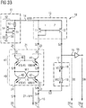
- FIG 3A shows an alternative exemplary embodiment of the voltage reference source 10 which is a further development of the embodiments shown in Figures 1 and 2 .
- the voltage reference source 10 comprises a capacitor 40 that is coupled to the first current mirror 13.
- the capacitor 40 connects a first terminal of the first mirror transistor 11 to a second terminal of the first mirror transistor 11.
- the capacitor 40 stabilizes a voltage across the controlled section of the first mirror transistor 11. Consequently, the capacitor 40 stabilizes the second signal S2 that flows as a current through the first mirror transistor 11 and, therefore, also the mirror current S3 flowing through the second mirror transistor 12.
- the voltage reference source 10 comprises a current source 41.
- the current source 41 is arranged between the fourth terminal 25 of the source block 21 and the supply voltage terminal 14.
- the current source 41 may be realized by a not shown source resistor 50.
- the source block 21 is implemented as a cross coupled quad. Quad means that the source block 21 comprises four transistors 42 - 45. The source block 21 may not comprise more transistors than four transistors. The source block 21 may be implemented as a cross coupled quad of bipolar transistors 42 - 45.
- the source block 21 comprises the first and the second series circuit 30, 31.
- the first series circuit 30 is arranged between the second terminal 23 and the first terminal 22 of the source block 21.
- the second series circuit 31 is arranged between the fourth terminal 25 and the third terminal 24 of the source block 21.
- the source block 21 comprises a first and a second transistor 42, 43 that are cross-coupled.
- the first and the second transistor 42, 43 form a cross coupled transistor pair 46.
- the first series circuit 30 comprises the first transistor 42, whereas the second series circuit 31 comprises the second transistor 43.
- a control terminal of the first transistor 42 is connected to a first terminal of the second transistor 43.
- a control terminal of the second transistor 43 is connected to a first terminal of the first transistor 42.
- the source block 21 comprises a third and a fourth mirror transistor 44, 45 forming a second current mirror 47.
- the third mirror transistor 44 is comprised by the first series circuit 30, whereas the fourth mirror transistor 45 is comprised by the second series circuit 31.
- the first transistor 42 is connected to the first terminal 22 of the source block 21, whereas the third mirror transistor 44 is connected to the second terminal 23 of the source block 21.
- the second transistor 43 is connected to the third terminal 24 of the source block 21, whereas the fourth mirror transistor 45 is connected to the fourth terminal 25 of the source block 21.
- a control terminal of the third mirror transistor 44 is connected to a control terminal of the fourth mirror transistor 45.
- the control terminal of the fourth mirror transistor 45 is also connected to a first terminal of the fourth mirror transistor 45 and thus to the fourth terminal 25 of the source block 21.
- the first and the second transistor 42, 43 and the third and the fourth mirror transistor 44, 45 are implemented as bipolar transistors. Said four transistors 42 - 45 may be implemented as npn bipolar transistors.
- the first and the second transistor 42, 43 and/or the third and the fourth mirror transistor 44, 45 are implemented as field-effect transistors.
- FIG 3B shows an alternative embodiment of the voltage reference source 10 which is a further development of the embodiments shown in Figures 1 , 2 and 3A .
- the capacitor 40 as shown in Figure 3A is omitted.
- the capacitor 40 is an optional device of the voltage reference source 10.
- the current source 41 comprises the source resistor 50 that is arranged between the fourth terminal 25 of the source block 21 and the supply voltage terminal 14. Moreover, the current source 41 comprises a source transistor 51 that is arranged in series to the source resistor 50. Moreover, the current source 41 comprises a current path 52 that couples the supply voltage terminal 14 to the reference potential terminal 20. A node of the current path 52 is connected to a control terminal of the source transistor 51. The source transistor 51 is connected to the fourth terminal 25 of the source block 21 and the source resistor 50 is connected to the supply voltage terminal 14.
- the current path 52 comprises a further source resistor 53 and a further source transistor 54 that are connected in series.
- the further source transistor 54 is connected to the supply voltage terminal 14, whereas the further source resistor 53 is connected to the reference potential terminal 20.
- a node between the further source resistor 53 and the further source transistor 54 is connected to the control terminal of the source transistor 51.
- a node between the controlled section of the source transistor 51 and the source resistor 50 is connected to a control terminal of the further source transistor 54.
- the current source 41 is implemented with a small number of devices.
- the current source 41 increases the power supply rejection ratio.
- the current source 41 may be implemented also by other current source circuits.
- the voltage reference source 10 comprises a buffer 55 that is connected on its input side to the reference output 15. At an output of the buffer 55, a buffered reference voltage S8 is provided.
- the voltage reference source 10 uses a cross-coupled quad of bipolar transistors 42 - 45 for generating the first signal S1.
- the first signal S1 is a PTAT voltage across the first resistor 16. Contrary to the voltage reference source 10 shown in Figure 4 , the branch with the diode 19 and the second resistor 18 is not connected to the reference potential terminal 20, said branch is fed back to the first resistor 16.
- a current signal S7 that is a current I1 through the second series circuit 31 of the transistors 43, 45 is generated by the current source 41.
- the current source 41 as shown in Figure 3B performs an improved power supply rejection.
- VBE45 is a base-emitter voltage of the fourth mirror transistor 45
- VBE42 is a base-emitter voltage of the first transistor 42
- VR1 is a voltage value of the first signal S1
- VBE44 is a base-emitter voltage of the third mirror transistor 44
- VBE43 is a base-emitter voltage of the second transistor 43
- VT is a thermal voltage
- the voltage value VR1 of the first signal S1 is equal to the voltage drop across the first resistor 16.
- 12 is a current value of the second signal S2 flowing through the second terminal 23 of the source block 21 and is also equal to the output current S4 flowing through the first terminal 22 of the source block 21.
- the factor M is defined such that a current driving capability of the fourth mirror transistor 45 is the M-fold of a current driving capability of the third mirror transistor 44.
- the factor M may be also named current mirror ratio of the second current mirror 47.
- the factor M may be larger than 1.
- the factor N is defined such that a current driving capability of the first transistor 42 is the N-fold of a current driving capability of the second transistor 43.
- the factor N may be larger than 1.
- the factor N may be also named cross coupled transistor ratio.
- the output branch comprising the diode 19 and the second resistor 18 is fed back into a node between the first resistor 16 and the first transistor 42.
- the mirror current S3 that is realized as a fed back current is a multiple of the collector current of the third mirror transistor 44 (current mirror ratio P).
- the noise gain for the noise from the first resistor 16 is the same as in the circuit shown in Figure 4 , if the current mirror ratio P is large. But due to the mirror current S3, the value of the first resistor 16 can be smaller especially for the same supply current and, therefore, the output noise of the reference voltage S6 is lower.
- the source block 21 is realized as the cross coupled quad and is designed for generation of the second signal S2 that is a PTAT current.
- the series connection 17 By connecting the series connection 17 to the first terminal of the first resistor 16, a feedback of the output branch of the voltage reference source 10 is realized.
- FIG 4 shows an alternative embodiment of the voltage reference source 10 which is a further development of the embodiments shown in Figures 1 , 2 , 3A and 3B and merely serves an illustrative purpose.
- the current source 51 is implemented by the source resistor 50. Thus, the current source 51 is free of any transistor.
- the series connection 17 is arranged between the reference output 15 and the reference potential terminal 20. Thus, the series connection 17 does not couple the reference output 15 to the first terminal of the first resistor 16. Consequently, the mirror current S3 flows through the series connection 17 directly to the reference potential terminal 20.
- the diode 19 is connected to the reference potential terminal 20, whereas the second resistor 18 is connected to the reference output 15.
- the diode 19 is connected to the reference output 15 and the second resistor 18 is connected to the reference potential terminal 20.
- the voltage reference source 10 is implemented as a Bandgap circuit.
- the voltage reference source 10 uses a cross-coupled quad of bipolar transistors 42-45 for generating a PTAT voltage across the first resistor 16.
- Another name for the cross-coupled quad is translinear loop TL.
- the cross-coupled quad is used for a PTAT current generator. Used in a Bandgap circuit, the PTAT current is mirrored into the output branch that comprises the diode 19 and the second resistor 18 by the first current mirror 13.
- the mirror current S3 realized as PTAT current through the second resistor 18 generates a voltage with positive temperature coefficient for compensating the negative temperature coefficient of the diode 19.
- FIGs 5A and 5B show exemplary embodiments of the diode 19.
- the diode 19 is implemented by a bipolar transistor 60.
- the diode 19 is realized by an npn-bipolar transistor.
- the base and the collector of the bipolar transistor 60 are connected together.
- the diode 19 is formed by the base-emitter junction of the bipolar transistor 60.
- the diode 19 is realized by a pnp-bipolar transistor.
- the base of the bipolar transistor 60 is connected to the collector of the bipolar transistor 60.
- the diode 19 is formed by the base-collector junction of the bipolar transistor 60.
- Figure 6 shows an exemplary characteristic of the voltage reference source 10.
- a base noise current is shown depending on the frequency and the current value. As shown at the lower frequency values, a 1/f noise occurs.
- the flicker noise exponent AFN has a value of 1.8.
- the current through the bipolar transistors 42 - 45 should be kept low due to their 1/f behavior.
- Figure 6 the noise of the base current of an npn transistor is depicted.
- the white noise current only increases with the square root of the emitter current, while the 1/f noise current increases almost proportional to the emitter current.
- the current through the transistors 42, 44 of the first series circuit 30 should be kept small, while for good white noise performance the current through the first resistor 16 should be large, resulting in a small resistance value for the first resistor 16. This can be accomplished in the voltage reference source 10 as shown in Figures 1 , 2 , 3A and 3B by choosing a large current mirror ratio of the first current mirror 14 (P>1).
- the added feedback loop leads to the following improved circuit properties: the noise of the first transistor 42 and of the third mirror transistor 44 may be attenuated.
- the noise of the third and the fourth mirror transistors 44, 45 may be attenuated.
- the noise of the first and the second mirror transistors 11, 12 may be attenuated. Therefore, the first to the fourth current mirror transistor 11, 12, 44, 45 can be kept small without increasing the 1/f noise level of the reference voltage S6.
- the matching requirement of the first current mirror 13 may be reduced. Also the matching requirement of the second current mirror 47 may be reduced.
- the reference output 15 at which the reference voltage S6 is tapped has a lower impedance.
- the voltage reference source 10 as shown in the Figures 3A , 3B and 4 implements a low noise voltage reference with cross-coupled quad bipolar transistors 42-45.
Landscapes
- Engineering & Computer Science (AREA)
- Physics & Mathematics (AREA)
- Microelectronics & Electronic Packaging (AREA)
- Nonlinear Science (AREA)
- Electromagnetism (AREA)
- General Physics & Mathematics (AREA)
- Radar, Positioning & Navigation (AREA)
- Automation & Control Theory (AREA)
- Power Engineering (AREA)
- Control Of Electrical Variables (AREA)
Claims (12)
- Spannungsreferenzquelle, umfassend:- einen Quellenblock (21),- einen ersten Widerstand (16) mit einem ersten Anschluss, der an einen ersten Anschluss (22) des Quellenblocks (21) angeschlossen ist, und einem zweiten Anschluss, der an einen Referenzpotentialanschluss (20) angeschlossen ist,- einen Referenzausgang (15), um eine Referenzspannung (S6) bereitzustellen,- einen ersten und einen zweiten Spiegeltransistor (11, 12), die einen ersten Stromspiegel (13) bilden, wobei der erste Spiegeltransistor (11) einen zweiten Anschluss (23) des Quellenblocks (21) an einen Versorgungsspannungsanschluss (14) anschließt, und der zweite Spiegeltransistor (12) den Referenzausgang (15) an den Versorgungsspannungsanschluss (14) anschließt, und- eine Reihenschaltung (17) aus einem zweiten Widerstand (18) und einer Diode (19), die zwischen dem Referenzausgang (15) und dem ersten Anschluss des ersten Widerstands (16) derart angeordnet ist, dass ein Spiegelstrom (S3) durch den zweiten Spiegeltransistor (12) und die Reihenschaltung (17) zum ersten Anschluss des ersten Widerstands (16) fließt,wobei der Quellenblock (21) einen dritten Anschluss (24) umfasst, der an den Referenzpotentialanschluss (20) angeschlossen ist, und
wobei der Quellenblock (21) einen ersten und einen zweiten Transistor (42, 43) derart umfasst, dass der erste Transistor (42) zwischen dem ersten Anschluss (22) des Quellenblocks (21) und dem zweiten Anschluss (23) des Quellenblocks (21) angeordnet ist, und der zweite Transistor (43) zwischen dem dritten Anschluss (24) des Quellenblocks (21) und einem vierten Anschluss (25) des Quellenblocks (21) angeordnet ist,
dadurch gekennzeichnet,
dass der vierte Anschluss (25) des Quellenblocks (21) an den Versorgungsspannungsanschluss (14) angeschlossen ist, wobei der erste und der zweite Transistor (42, 43) des Quellenblocks (21) kreuzgekoppelt sind. - Spannungsreferenzquelle nach Anspruch 1,
wobei der Quellenblock (21) dazu konfiguriert ist, ein erstes Signal (S1) am ersten Anschluss (22) des Quellenblocks (21) bereitzustellen, das als Spannung implementiert ist, die proportional zur absoluten Temperatur ist. - Spannungsreferenzquelle nach Anspruch 1 oder 2,
wobei der Quellenblock (21) dazu konfiguriert ist, ein zweites Signal (S2) am zweiten Anschluss (23) des Quellenblocks (21) bereitzustellen, das als Strom implementiert ist, der proportional zur absoluten Temperatur ist und durch den zweiten Anschluss (23) des Quellenblocks (21) fließt. - Spannungsreferenzquelle nach einem der Ansprüche 1 bis 3,
wobei eine Stromantriebsfähigkeit des zweiten Spiegeltransistors (13) das P-fache einer Stromantriebsfähigkeit des ersten Spiegeltransistors (12) beträgt und der Faktor P größer als 1 ist. - Spannungsreferenzquelle nach einem der Ansprüche 1 bis 4,
wobei ein Steueranschluss des ersten Spiegeltransistors (11) direkt mit einen Steueranschluss des zweiten Spiegeltransistors (12) verbunden ist. - Spannungsreferenzquelle nach einem der Ansprüche 1 bis 5,
wobei der erste und der zweite Spiegeltransistor (11, 12) beide als Feldeffekttransistoren implementiert sind, oder beide als Bipolartransistoren implementiert sind. - Spannungsreferenzquelle nach einem der Ansprüche 1 bis 6, eine Stromquelle (41) umfassend, die den vierten Anschluss (25) des Quellenblocks (21) an den Versorgungsspannungsanschluss (14) anschließt.
- Spannungsreferenzquelle nach Anspruch 7,
wobei die Stromquelle (41) einen Quellenwiderstand (50) umfasst, der zwischen dem vierten Anschluss (25) des Quellenblocks (21) und dem Versorgungsspannungsanschluss (14) angeordnet ist. - Spannungsreferenzquelle nach einem der Ansprüche 1 bis 8,
wobei eine Stromantriebsfähigkeit des ersten Transistors (42) das N-fache einer Stromantriebsfähigkeit des zweiten Transistors (43) beträgt und der Faktor N größer als 1 ist. - Spannungsreferenzquelle nach Anspruch 8 oder 9,
wobei der Quellenblock (21) einen dritten und einen vierten Spiegeltransistor (44, 45) umfasst, die einen zweiten Stromspiegel (47) bilden, und der dritte Spiegeltransistor (44) in Reihe zum ersten Transistor (42) angeordnet ist, und der vierte Spiegeltransistor (45) in Reihe zum zweiten Transistor (43) angeordnet ist. - Spannungsreferenzquelle nach Anspruch 10,
wobei eine Stromantriebsfähigkeit des vierten Spiegeltransistors (45) das M-fache einer
Stromantriebsfähigkeit des dritten Spiegeltransistors (44) beträgt und der Faktor M größer als 1 ist. - Verfahren zum Generieren einer Referenzspannung, umfassend:- Bereitstellen eines ersten Signals (S1) an einem ersten Anschluss (22) eines Quellenblocks (21), wobei der erste Anschluss (22) des Quellenblocks (21) an einen ersten Anschluss eines ersten Widerstands (16) angeschlossen ist, und ein zweiter Anschluss des ersten Widerstands (16) an einen Referenzpotentialanschluss (20) angeschlossen ist,- Bereitstellen eines als Strom implementierten zweiten Signals (S2) an einem zweiten Anschluss (23) des Quellenblocks (21),- Spiegeln des zweiten Signals (S2) in einen Spiegelstrom (S3) durch einen ersten Stromspiegel (13), der einen ersten und einen zweiten Spiegeltransistor (11, 12) umfasst, und zwar derart, dass der erste Spiegeltransistor (11) den zweiten Anschluss (23) des Quellenblocks (21) an einen Versorgungsspannungsanschluss (14) anschließt, und der zweite Spiegeltransistor (12) einen Referenzausgang (15) an den Versorgungsspannungsanschluss (14) anschließt,- Bereitstellen des Spiegelstroms (S3) über eine Reihenschaltung (17) aus einem zweiten Widerstand (18) und einer Diode (19) an den ersten Anschluss des ersten Widerstands (16), und- Bereitstellen der Referenzspannung (S6) am Referenzausgang (15),wobei der Quellenblock (21) einen dritten Anschluss (24) umfasst, der an den Referenzpotentialanschluss (20) angeschlossen ist, und
wobei der Quellenblock (21) einen ersten und einen zweiten Transistor (42, 43) derart umfasst, dass der erste Transistor (42) zwischen dem ersten Anschluss (22) des Quellenblocks (21) und dem zweiten Anschluss (23) des Quellenblocks (21) angeordnet ist, und der zweite Transistor (43) zwischen dem dritten Anschluss (24) des Quellenblocks (21) und einem vierten Anschluss (25) des Quellenblocks (21) angeordnet ist,
dadurch gekennzeichnet,
dass der vierte Anschluss (25) des Quellenblocks (21) an den Versorgungsspannungsanschluss (14) angeschlossen ist, wobei der erste und der zweite Transistor (42, 43) des Quellenblocks (21) kreuzgekoppelt sind.
Priority Applications (2)
| Application Number | Priority Date | Filing Date | Title |
|---|---|---|---|
| EP14193251.7A EP3021189B1 (de) | 2014-11-14 | 2014-11-14 | Spannungsreferenzquelle und Verfahren zur Erzeugung einer Referenzspannung |
| US14/940,079 US9753482B2 (en) | 2014-11-14 | 2015-11-12 | Voltage reference source and method for generating a reference voltage |
Applications Claiming Priority (1)
| Application Number | Priority Date | Filing Date | Title |
|---|---|---|---|
| EP14193251.7A EP3021189B1 (de) | 2014-11-14 | 2014-11-14 | Spannungsreferenzquelle und Verfahren zur Erzeugung einer Referenzspannung |
Publications (2)
| Publication Number | Publication Date |
|---|---|
| EP3021189A1 EP3021189A1 (de) | 2016-05-18 |
| EP3021189B1 true EP3021189B1 (de) | 2020-12-30 |
Family
ID=51893938
Family Applications (1)
| Application Number | Title | Priority Date | Filing Date |
|---|---|---|---|
| EP14193251.7A Active EP3021189B1 (de) | 2014-11-14 | 2014-11-14 | Spannungsreferenzquelle und Verfahren zur Erzeugung einer Referenzspannung |
Country Status (2)
| Country | Link |
|---|---|
| US (1) | US9753482B2 (de) |
| EP (1) | EP3021189B1 (de) |
Families Citing this family (7)
| Publication number | Priority date | Publication date | Assignee | Title |
|---|---|---|---|---|
| EP3091418B1 (de) * | 2015-05-08 | 2023-04-19 | STMicroelectronics S.r.l. | Schaltungsanordnung zur erzeugung eines referenzspannungsbandabstands |
| KR102737705B1 (ko) * | 2020-03-31 | 2024-12-03 | 에스케이하이닉스 주식회사 | 기준 전압 회로 |
| EP3929694B1 (de) * | 2020-06-22 | 2023-08-30 | NXP USA, Inc. | Spannungsregler |
| CN114690841A (zh) * | 2020-12-28 | 2022-07-01 | 中国科学院微电子研究所 | 一种基准电流产生电路及模拟集成电路系统 |
| CN114690842B (zh) * | 2020-12-29 | 2024-07-02 | 圣邦微电子(北京)股份有限公司 | 一种用于偏置双极型晶体管的电流源电路 |
| GB202107532D0 (en) * | 2021-05-27 | 2021-07-14 | Ams Sensors Singapore Pte Ltd | Circuit for device temperature protection |
| CN118034443A (zh) * | 2024-03-14 | 2024-05-14 | 西安电子科技大学 | 一种自偏置结构的ptat电流产生电路 |
Family Cites Families (32)
| Publication number | Priority date | Publication date | Assignee | Title |
|---|---|---|---|---|
| US3887863A (en) | 1973-11-28 | 1975-06-03 | Analog Devices Inc | Solid-state regulated voltage supply |
| NL8200974A (nl) * | 1982-03-10 | 1983-10-03 | Philips Nv | Stroomdiskriminatie-schakeling. |
| US4636710A (en) * | 1985-10-15 | 1987-01-13 | Silvo Stanojevic | Stacked bandgap voltage reference |
| US4689549A (en) * | 1986-06-30 | 1987-08-25 | Motorola, Inc. | Monolithic current splitter for providing temperature independent current ratios |
| DE19818464A1 (de) * | 1998-04-24 | 1999-10-28 | Siemens Ag | Referenzspannung-Erzeugungsschaltung |
| US6285244B1 (en) | 1999-10-02 | 2001-09-04 | Texas Instruments Incorporated | Low voltage, VCC incentive, low temperature co-efficient, stable cross-coupled bandgap circuit |
| US6462526B1 (en) | 2001-08-01 | 2002-10-08 | Maxim Integrated Products, Inc. | Low noise bandgap voltage reference circuit |
| US6972550B2 (en) * | 2001-10-10 | 2005-12-06 | Taiwan Semiconductor Manufacturing Co., Ltd. | Bandgap reference voltage generator with a low-cost, low-power, fast start-up circuit |
| DE10233526A1 (de) * | 2002-07-23 | 2004-02-12 | Infineon Technologies Ag | Bandabstands-Referenzschaltung |
| US7170337B2 (en) * | 2004-04-20 | 2007-01-30 | Sige Semiconductor (U.S.), Corp. | Low voltage wide ratio current mirror |
| JP2006133916A (ja) * | 2004-11-02 | 2006-05-25 | Nec Electronics Corp | 基準電圧回路 |
| JP4780968B2 (ja) * | 2005-01-25 | 2011-09-28 | ルネサスエレクトロニクス株式会社 | 基準電圧回路 |
| US7242240B2 (en) * | 2005-05-05 | 2007-07-10 | Agere Systems, Inc. | Low noise bandgap circuit |
| JP2008015925A (ja) * | 2006-07-07 | 2008-01-24 | Matsushita Electric Ind Co Ltd | 基準電圧発生回路 |
| JP4499696B2 (ja) * | 2006-09-15 | 2010-07-07 | Okiセミコンダクタ株式会社 | 基準電流生成装置 |
| JP2008108009A (ja) * | 2006-10-24 | 2008-05-08 | Matsushita Electric Ind Co Ltd | 基準電圧発生回路 |
| US20090039949A1 (en) | 2007-08-09 | 2009-02-12 | Giovanni Pietrobon | Method and apparatus for producing a low-noise, temperature-compensated bandgap voltage reference |
| US7839202B2 (en) * | 2007-10-02 | 2010-11-23 | Qualcomm, Incorporated | Bandgap reference circuit with reduced power consumption |
| JP2009251877A (ja) * | 2008-04-04 | 2009-10-29 | Nec Electronics Corp | 基準電圧回路 |
| US7944280B2 (en) * | 2008-05-26 | 2011-05-17 | International Business Machines Corporation | Bandgap reference generator utilizing a current trimming circuit |
| KR101241378B1 (ko) * | 2008-12-05 | 2013-03-07 | 한국전자통신연구원 | 기준 바이어스 발생 회로 |
| JP5035391B2 (ja) * | 2010-01-12 | 2012-09-26 | 株式会社デンソー | 信号出力回路 |
| US8421433B2 (en) | 2010-03-31 | 2013-04-16 | Maxim Integrated Products, Inc. | Low noise bandgap references |
| US8648648B2 (en) * | 2010-12-30 | 2014-02-11 | Stmicroelectronics, Inc. | Bandgap voltage reference circuit, system, and method for reduced output curvature |
| EP2557472B1 (de) | 2011-08-12 | 2017-04-05 | ams AG | Signalgenerator und Verfahren zur Signalerzeugung |
| US9092044B2 (en) * | 2011-11-01 | 2015-07-28 | Silicon Storage Technology, Inc. | Low voltage, low power bandgap circuit |
| US8698479B2 (en) * | 2012-03-30 | 2014-04-15 | Elite Semiconductor Memory Technology Inc. | Bandgap reference circuit for providing reference voltage |
| US9170595B2 (en) * | 2012-10-12 | 2015-10-27 | Stmicroelectronics International N.V. | Low power reference generator circuit |
| US9122290B2 (en) * | 2013-03-15 | 2015-09-01 | Intel Deutschland Gmbh | Bandgap reference circuit |
| TWI521326B (zh) * | 2013-12-27 | 2016-02-11 | 慧榮科技股份有限公司 | 帶隙參考電壓產生電路 |
| EP2977849B8 (de) * | 2014-07-24 | 2025-08-06 | Renesas Design (UK) Limited | Hochspannungs- zu Niederspannungsregler mit niedrigem Spannungsverlust mit autarker Spannungsreferenz |
| US20160266598A1 (en) * | 2015-03-10 | 2016-09-15 | Qualcomm Incorporated | Precision bandgap reference |
-
2014
- 2014-11-14 EP EP14193251.7A patent/EP3021189B1/de active Active
-
2015
- 2015-11-12 US US14/940,079 patent/US9753482B2/en active Active
Non-Patent Citations (1)
| Title |
|---|
| None * |
Also Published As
| Publication number | Publication date |
|---|---|
| US9753482B2 (en) | 2017-09-05 |
| EP3021189A1 (de) | 2016-05-18 |
| US20160139621A1 (en) | 2016-05-19 |
Similar Documents
| Publication | Publication Date | Title |
|---|---|---|
| EP3021189B1 (de) | Spannungsreferenzquelle und Verfahren zur Erzeugung einer Referenzspannung | |
| KR0169316B1 (ko) | 기준 발생기 | |
| US6774711B2 (en) | Low power bandgap voltage reference circuit | |
| US9459647B2 (en) | Bandgap reference circuit and bandgap reference current source with two operational amplifiers for generating zero temperature correlated current | |
| US10296026B2 (en) | Low noise reference voltage generator and load regulator | |
| US7902912B2 (en) | Bias current generator | |
| US8786271B2 (en) | Circuit and method for generating reference voltage and reference current | |
| JP2008108009A (ja) | 基準電圧発生回路 | |
| US9489004B2 (en) | Bandgap reference voltage generator circuits | |
| US7161340B2 (en) | Method and apparatus for generating N-order compensated temperature independent reference voltage | |
| US10379567B2 (en) | Bandgap reference circuitry | |
| US8089260B2 (en) | Low voltage bandgap reference circuit | |
| US7944272B2 (en) | Constant current circuit | |
| US9600013B1 (en) | Bandgap reference circuit | |
| JPH02178716A (ja) | 電圧発生回路 | |
| US8884601B2 (en) | System and method for a low voltage bandgap reference | |
| US6175224B1 (en) | Regulator circuit having a bandgap generator coupled to a voltage sensor, and method | |
| CN115357088B (zh) | 一种具有简易结构的低温度系数供电电路 | |
| JP2021125091A (ja) | 基準電圧回路 | |
| JP2007305010A (ja) | 基準電圧生成回路 | |
| TWI716323B (zh) | 電壓產生器 | |
| US20120153997A1 (en) | Circuit for Generating a Reference Voltage Under a Low Power Supply Voltage | |
| KR101980526B1 (ko) | 기준 전류 발생 회로 및 기준 전압 발생 회로 | |
| JP6864516B2 (ja) | レギュレータ回路 | |
| JP2006031246A (ja) | 基準電流発生回路 |
Legal Events
| Date | Code | Title | Description |
|---|---|---|---|
| PUAI | Public reference made under article 153(3) epc to a published international application that has entered the european phase |
Free format text: ORIGINAL CODE: 0009012 |
|
| AK | Designated contracting states |
Kind code of ref document: A1 Designated state(s): AL AT BE BG CH CY CZ DE DK EE ES FI FR GB GR HR HU IE IS IT LI LT LU LV MC MK MT NL NO PL PT RO RS SE SI SK SM TR |
|
| AX | Request for extension of the european patent |
Extension state: BA ME |
|
| STAA | Information on the status of an ep patent application or granted ep patent |
Free format text: STATUS: REQUEST FOR EXAMINATION WAS MADE |
|
| 17P | Request for examination filed |
Effective date: 20161116 |
|
| RBV | Designated contracting states (corrected) |
Designated state(s): AL AT BE BG CH CY CZ DE DK EE ES FI FR GB GR HR HU IE IS IT LI LT LU LV MC MK MT NL NO PL PT RO RS SE SI SK SM TR |
|
| RAP1 | Party data changed (applicant data changed or rights of an application transferred) |
Owner name: AMS AG |
|
| GRAP | Despatch of communication of intention to grant a patent |
Free format text: ORIGINAL CODE: EPIDOSNIGR1 |
|
| STAA | Information on the status of an ep patent application or granted ep patent |
Free format text: STATUS: GRANT OF PATENT IS INTENDED |
|
| INTG | Intention to grant announced |
Effective date: 20200729 |
|
| GRAS | Grant fee paid |
Free format text: ORIGINAL CODE: EPIDOSNIGR3 |
|
| GRAA | (expected) grant |
Free format text: ORIGINAL CODE: 0009210 |
|
| STAA | Information on the status of an ep patent application or granted ep patent |
Free format text: STATUS: THE PATENT HAS BEEN GRANTED |
|
| AK | Designated contracting states |
Kind code of ref document: B1 Designated state(s): AL AT BE BG CH CY CZ DE DK EE ES FI FR GB GR HR HU IE IS IT LI LT LU LV MC MK MT NL NO PL PT RO RS SE SI SK SM TR |
|
| REG | Reference to a national code |
Ref country code: GB Ref legal event code: FG4D |
|
| RIN1 | Information on inventor provided before grant (corrected) |
Inventor name: MUELLER, THOMAS Inventor name: NIEDERBERGER, MARK |
|
| REG | Reference to a national code |
Ref country code: DE Ref legal event code: R096 Ref document number: 602014073760 Country of ref document: DE |
|
| REG | Reference to a national code |
Ref country code: AT Ref legal event code: REF Ref document number: 1350568 Country of ref document: AT Kind code of ref document: T Effective date: 20210115 |
|
| REG | Reference to a national code |
Ref country code: IE Ref legal event code: FG4D |
|
| PG25 | Lapsed in a contracting state [announced via postgrant information from national office to epo] |
Ref country code: NO Free format text: LAPSE BECAUSE OF FAILURE TO SUBMIT A TRANSLATION OF THE DESCRIPTION OR TO PAY THE FEE WITHIN THE PRESCRIBED TIME-LIMIT Effective date: 20210330 Ref country code: RS Free format text: LAPSE BECAUSE OF FAILURE TO SUBMIT A TRANSLATION OF THE DESCRIPTION OR TO PAY THE FEE WITHIN THE PRESCRIBED TIME-LIMIT Effective date: 20201230 Ref country code: FI Free format text: LAPSE BECAUSE OF FAILURE TO SUBMIT A TRANSLATION OF THE DESCRIPTION OR TO PAY THE FEE WITHIN THE PRESCRIBED TIME-LIMIT Effective date: 20201230 Ref country code: GR Free format text: LAPSE BECAUSE OF FAILURE TO SUBMIT A TRANSLATION OF THE DESCRIPTION OR TO PAY THE FEE WITHIN THE PRESCRIBED TIME-LIMIT Effective date: 20210331 |
|
| REG | Reference to a national code |
Ref country code: AT Ref legal event code: MK05 Ref document number: 1350568 Country of ref document: AT Kind code of ref document: T Effective date: 20201230 |
|
| PG25 | Lapsed in a contracting state [announced via postgrant information from national office to epo] |
Ref country code: SE Free format text: LAPSE BECAUSE OF FAILURE TO SUBMIT A TRANSLATION OF THE DESCRIPTION OR TO PAY THE FEE WITHIN THE PRESCRIBED TIME-LIMIT Effective date: 20201230 Ref country code: LV Free format text: LAPSE BECAUSE OF FAILURE TO SUBMIT A TRANSLATION OF THE DESCRIPTION OR TO PAY THE FEE WITHIN THE PRESCRIBED TIME-LIMIT Effective date: 20201230 Ref country code: BG Free format text: LAPSE BECAUSE OF FAILURE TO SUBMIT A TRANSLATION OF THE DESCRIPTION OR TO PAY THE FEE WITHIN THE PRESCRIBED TIME-LIMIT Effective date: 20210330 |
|
| REG | Reference to a national code |
Ref country code: NL Ref legal event code: MP Effective date: 20201230 |
|
| PG25 | Lapsed in a contracting state [announced via postgrant information from national office to epo] |
Ref country code: HR Free format text: LAPSE BECAUSE OF FAILURE TO SUBMIT A TRANSLATION OF THE DESCRIPTION OR TO PAY THE FEE WITHIN THE PRESCRIBED TIME-LIMIT Effective date: 20201230 |
|
| REG | Reference to a national code |
Ref country code: LT Ref legal event code: MG9D |
|
| PG25 | Lapsed in a contracting state [announced via postgrant information from national office to epo] |
Ref country code: LT Free format text: LAPSE BECAUSE OF FAILURE TO SUBMIT A TRANSLATION OF THE DESCRIPTION OR TO PAY THE FEE WITHIN THE PRESCRIBED TIME-LIMIT Effective date: 20201230 Ref country code: SK Free format text: LAPSE BECAUSE OF FAILURE TO SUBMIT A TRANSLATION OF THE DESCRIPTION OR TO PAY THE FEE WITHIN THE PRESCRIBED TIME-LIMIT Effective date: 20201230 Ref country code: PT Free format text: LAPSE BECAUSE OF FAILURE TO SUBMIT A TRANSLATION OF THE DESCRIPTION OR TO PAY THE FEE WITHIN THE PRESCRIBED TIME-LIMIT Effective date: 20210430 Ref country code: RO Free format text: LAPSE BECAUSE OF FAILURE TO SUBMIT A TRANSLATION OF THE DESCRIPTION OR TO PAY THE FEE WITHIN THE PRESCRIBED TIME-LIMIT Effective date: 20201230 Ref country code: CZ Free format text: LAPSE BECAUSE OF FAILURE TO SUBMIT A TRANSLATION OF THE DESCRIPTION OR TO PAY THE FEE WITHIN THE PRESCRIBED TIME-LIMIT Effective date: 20201230 Ref country code: EE Free format text: LAPSE BECAUSE OF FAILURE TO SUBMIT A TRANSLATION OF THE DESCRIPTION OR TO PAY THE FEE WITHIN THE PRESCRIBED TIME-LIMIT Effective date: 20201230 Ref country code: NL Free format text: LAPSE BECAUSE OF FAILURE TO SUBMIT A TRANSLATION OF THE DESCRIPTION OR TO PAY THE FEE WITHIN THE PRESCRIBED TIME-LIMIT Effective date: 20201230 |
|
| PG25 | Lapsed in a contracting state [announced via postgrant information from national office to epo] |
Ref country code: AT Free format text: LAPSE BECAUSE OF FAILURE TO SUBMIT A TRANSLATION OF THE DESCRIPTION OR TO PAY THE FEE WITHIN THE PRESCRIBED TIME-LIMIT Effective date: 20201230 Ref country code: PL Free format text: LAPSE BECAUSE OF FAILURE TO SUBMIT A TRANSLATION OF THE DESCRIPTION OR TO PAY THE FEE WITHIN THE PRESCRIBED TIME-LIMIT Effective date: 20201230 |
|
| PG25 | Lapsed in a contracting state [announced via postgrant information from national office to epo] |
Ref country code: IS Free format text: LAPSE BECAUSE OF FAILURE TO SUBMIT A TRANSLATION OF THE DESCRIPTION OR TO PAY THE FEE WITHIN THE PRESCRIBED TIME-LIMIT Effective date: 20210430 |
|
| REG | Reference to a national code |
Ref country code: DE Ref legal event code: R097 Ref document number: 602014073760 Country of ref document: DE |
|
| PG25 | Lapsed in a contracting state [announced via postgrant information from national office to epo] |
Ref country code: IT Free format text: LAPSE BECAUSE OF FAILURE TO SUBMIT A TRANSLATION OF THE DESCRIPTION OR TO PAY THE FEE WITHIN THE PRESCRIBED TIME-LIMIT Effective date: 20201230 Ref country code: AL Free format text: LAPSE BECAUSE OF FAILURE TO SUBMIT A TRANSLATION OF THE DESCRIPTION OR TO PAY THE FEE WITHIN THE PRESCRIBED TIME-LIMIT Effective date: 20201230 |
|
| PLBE | No opposition filed within time limit |
Free format text: ORIGINAL CODE: 0009261 |
|
| STAA | Information on the status of an ep patent application or granted ep patent |
Free format text: STATUS: NO OPPOSITION FILED WITHIN TIME LIMIT |
|
| PG25 | Lapsed in a contracting state [announced via postgrant information from national office to epo] |
Ref country code: ES Free format text: LAPSE BECAUSE OF FAILURE TO SUBMIT A TRANSLATION OF THE DESCRIPTION OR TO PAY THE FEE WITHIN THE PRESCRIBED TIME-LIMIT Effective date: 20201230 Ref country code: DK Free format text: LAPSE BECAUSE OF FAILURE TO SUBMIT A TRANSLATION OF THE DESCRIPTION OR TO PAY THE FEE WITHIN THE PRESCRIBED TIME-LIMIT Effective date: 20201230 |
|
| 26N | No opposition filed |
Effective date: 20211001 |
|
| PG25 | Lapsed in a contracting state [announced via postgrant information from national office to epo] |
Ref country code: SI Free format text: LAPSE BECAUSE OF FAILURE TO SUBMIT A TRANSLATION OF THE DESCRIPTION OR TO PAY THE FEE WITHIN THE PRESCRIBED TIME-LIMIT Effective date: 20201230 |
|
| PG25 | Lapsed in a contracting state [announced via postgrant information from national office to epo] |
Ref country code: IS Free format text: LAPSE BECAUSE OF FAILURE TO SUBMIT A TRANSLATION OF THE DESCRIPTION OR TO PAY THE FEE WITHIN THE PRESCRIBED TIME-LIMIT Effective date: 20210430 |
|
| PG25 | Lapsed in a contracting state [announced via postgrant information from national office to epo] |
Ref country code: MC Free format text: LAPSE BECAUSE OF FAILURE TO SUBMIT A TRANSLATION OF THE DESCRIPTION OR TO PAY THE FEE WITHIN THE PRESCRIBED TIME-LIMIT Effective date: 20201230 |
|
| REG | Reference to a national code |
Ref country code: CH Ref legal event code: PL |
|
| PG25 | Lapsed in a contracting state [announced via postgrant information from national office to epo] |
Ref country code: LU Free format text: LAPSE BECAUSE OF NON-PAYMENT OF DUE FEES Effective date: 20211114 Ref country code: BE Free format text: LAPSE BECAUSE OF NON-PAYMENT OF DUE FEES Effective date: 20211130 |
|
| REG | Reference to a national code |
Ref country code: BE Ref legal event code: MM Effective date: 20211130 |
|
| PG25 | Lapsed in a contracting state [announced via postgrant information from national office to epo] |
Ref country code: LI Free format text: LAPSE BECAUSE OF NON-PAYMENT OF DUE FEES Effective date: 20211130 Ref country code: CH Free format text: LAPSE BECAUSE OF NON-PAYMENT OF DUE FEES Effective date: 20211130 |
|
| PG25 | Lapsed in a contracting state [announced via postgrant information from national office to epo] |
Ref country code: IE Free format text: LAPSE BECAUSE OF NON-PAYMENT OF DUE FEES Effective date: 20211114 |
|
| PG25 | Lapsed in a contracting state [announced via postgrant information from national office to epo] |
Ref country code: FR Free format text: LAPSE BECAUSE OF NON-PAYMENT OF DUE FEES Effective date: 20211130 |
|
| PG25 | Lapsed in a contracting state [announced via postgrant information from national office to epo] |
Ref country code: HU Free format text: LAPSE BECAUSE OF FAILURE TO SUBMIT A TRANSLATION OF THE DESCRIPTION OR TO PAY THE FEE WITHIN THE PRESCRIBED TIME-LIMIT; INVALID AB INITIO Effective date: 20141114 |
|
| PG25 | Lapsed in a contracting state [announced via postgrant information from national office to epo] |
Ref country code: CY Free format text: LAPSE BECAUSE OF FAILURE TO SUBMIT A TRANSLATION OF THE DESCRIPTION OR TO PAY THE FEE WITHIN THE PRESCRIBED TIME-LIMIT Effective date: 20201230 |
|
| PG25 | Lapsed in a contracting state [announced via postgrant information from national office to epo] |
Ref country code: SM Free format text: LAPSE BECAUSE OF FAILURE TO SUBMIT A TRANSLATION OF THE DESCRIPTION OR TO PAY THE FEE WITHIN THE PRESCRIBED TIME-LIMIT Effective date: 20201230 |
|
| P01 | Opt-out of the competence of the unified patent court (upc) registered |
Effective date: 20230822 |
|
| PG25 | Lapsed in a contracting state [announced via postgrant information from national office to epo] |
Ref country code: MK Free format text: LAPSE BECAUSE OF FAILURE TO SUBMIT A TRANSLATION OF THE DESCRIPTION OR TO PAY THE FEE WITHIN THE PRESCRIBED TIME-LIMIT Effective date: 20201230 |
|
| PG25 | Lapsed in a contracting state [announced via postgrant information from national office to epo] |
Ref country code: MT Free format text: LAPSE BECAUSE OF FAILURE TO SUBMIT A TRANSLATION OF THE DESCRIPTION OR TO PAY THE FEE WITHIN THE PRESCRIBED TIME-LIMIT Effective date: 20201230 |
|
| PG25 | Lapsed in a contracting state [announced via postgrant information from national office to epo] |
Ref country code: TR Free format text: LAPSE BECAUSE OF FAILURE TO SUBMIT A TRANSLATION OF THE DESCRIPTION OR TO PAY THE FEE WITHIN THE PRESCRIBED TIME-LIMIT Effective date: 20201230 |
|
| PGFP | Annual fee paid to national office [announced via postgrant information from national office to epo] |
Ref country code: DE Payment date: 20251119 Year of fee payment: 12 |
|
| PGFP | Annual fee paid to national office [announced via postgrant information from national office to epo] |
Ref country code: GB Payment date: 20251121 Year of fee payment: 12 |