EP3017501B1 - Antennas with shared grounding structure - Google Patents
Antennas with shared grounding structure Download PDFInfo
- Publication number
- EP3017501B1 EP3017501B1 EP14736264.4A EP14736264A EP3017501B1 EP 3017501 B1 EP3017501 B1 EP 3017501B1 EP 14736264 A EP14736264 A EP 14736264A EP 3017501 B1 EP3017501 B1 EP 3017501B1
- Authority
- EP
- European Patent Office
- Prior art keywords
- monopole
- elements
- antenna
- connecting strip
- coupled
- Prior art date
- Legal status (The legal status is an assumption and is not a legal conclusion. Google has not performed a legal analysis and makes no representation as to the accuracy of the status listed.)
- Active
Links
Images


Classifications
-
- H—ELECTRICITY
- H01—ELECTRIC ELEMENTS
- H01Q—ANTENNAS, i.e. RADIO AERIALS
- H01Q21/00—Antenna arrays or systems
- H01Q21/0006—Particular feeding systems
-
- H—ELECTRICITY
- H01—ELECTRIC ELEMENTS
- H01Q—ANTENNAS, i.e. RADIO AERIALS
- H01Q1/00—Details of, or arrangements associated with, antennas
- H01Q1/12—Supports; Mounting means
- H01Q1/22—Supports; Mounting means by structural association with other equipment or articles
- H01Q1/24—Supports; Mounting means by structural association with other equipment or articles with receiving set
- H01Q1/241—Supports; Mounting means by structural association with other equipment or articles with receiving set used in mobile communications, e.g. GSM
- H01Q1/242—Supports; Mounting means by structural association with other equipment or articles with receiving set used in mobile communications, e.g. GSM specially adapted for hand-held use
- H01Q1/243—Supports; Mounting means by structural association with other equipment or articles with receiving set used in mobile communications, e.g. GSM specially adapted for hand-held use with built-in antennas
-
- H—ELECTRICITY
- H01—ELECTRIC ELEMENTS
- H01Q—ANTENNAS, i.e. RADIO AERIALS
- H01Q1/00—Details of, or arrangements associated with, antennas
- H01Q1/48—Earthing means; Earth screens; Counterpoises
-
- H—ELECTRICITY
- H01—ELECTRIC ELEMENTS
- H01Q—ANTENNAS, i.e. RADIO AERIALS
- H01Q1/00—Details of, or arrangements associated with, antennas
- H01Q1/52—Means for reducing coupling between antennas; Means for reducing coupling between an antenna and another structure
- H01Q1/521—Means for reducing coupling between antennas; Means for reducing coupling between an antenna and another structure reducing the coupling between adjacent antennas
-
- H—ELECTRICITY
- H01—ELECTRIC ELEMENTS
- H01Q—ANTENNAS, i.e. RADIO AERIALS
- H01Q21/00—Antenna arrays or systems
- H01Q21/28—Combinations of substantially independent non-interacting antenna units or systems
-
- Y—GENERAL TAGGING OF NEW TECHNOLOGICAL DEVELOPMENTS; GENERAL TAGGING OF CROSS-SECTIONAL TECHNOLOGIES SPANNING OVER SEVERAL SECTIONS OF THE IPC; TECHNICAL SUBJECTS COVERED BY FORMER USPC CROSS-REFERENCE ART COLLECTIONS [XRACs] AND DIGESTS
- Y10—TECHNICAL SUBJECTS COVERED BY FORMER USPC
- Y10T—TECHNICAL SUBJECTS COVERED BY FORMER US CLASSIFICATION
- Y10T29/00—Metal working
- Y10T29/49—Method of mechanical manufacture
- Y10T29/49002—Electrical device making
- Y10T29/49016—Antenna or wave energy "plumbing" making
Definitions
- the disclosure relates to antennas for wireless communications devices.
- State-of-the-art wireless communications devices such as smart phones often require broadband antennas to accommodate multiple frequency bands, e.g., as dictated by the long-term evolution (LTE) system and other existing wireless wide area network (WWAN) mobile networks.
- LTE long-term evolution
- WWAN wireless wide area network
- LTE 700 (698-787 MHz)
- GSM 850 (824-894 MHz
- GSM 900 (880-960 MHz)
- a wireless device may be required to process radio signals over as many as eight or nine frequency bands, or more.
- wireless devices may employ antennas operating over two or more broad bands that collectively cover the above-mentioned frequency bands, e.g., a low broad band spanning 700MHz-960MHz and a high broad band spanning 1710MHz-2690MHz.
- a small antenna size usually corresponds to narrow bandwidth and low radiation efficiency. Accordingly, to accommodate such a broad bandwidth, each antenna requires a minimum volume or clearance, which mandates a minimum size for the design.
- multiple antennas are required to implement a feature known as multiple-input multiple-output (MIMO) to enhance wireless channel capacity.
- MIMO multiple-input multiple-output
- a wireless device may typically be required to include two or more antennas.
- ID industry design
- very limited internal space within the wireless device is left for the antennas.
- WO 2010/028521 A is directed to an antenna system comprising a first antenna element mutually coupled with a second antenna element, the mutual coupling between the first and second antenna elements causing a first current in the second antenna element, and a coupling element disposed at least partially between the first and second antenna elements, wherein the coupling element is mutually coupled to each of the first and second antenna elements, and wherein the coupling element is configured to induce a second current in the second antenna element that at least partially cancels the first current
- US 2013/0050027 A1 is directed to a MIMO/diversity antenna with high isolation including a printed circuit board, a plurality of antenna elements, a current conversion element connected with a common ground of the printed circuit board apart from the antenna elements at a predetermined distance, wherein the current conversion element is coupled with the antenna elements to induce an electric current from the antenna elements into the antenna elements again via the common ground.
- WO 2013/0101045 A1 Attention is drawn to WO 2013/0101045 A1 , which is directed to a wideband antenna system with multiple antennas and at least one parasitic element.
- FIG 1 illustrates a block diagram of a design of a prior art wireless communication device 100 in which the techniques of the present disclosure may be implemented.
- FIG 1 shows an example transceiver design.
- the conditioning of the signals in a transmitter and a receiver may be performed by one or more stages of amplifier, filter, upconverter, downconverter, etc.
- These circuit blocks may be arranged differently from the configuration shown in FIG 1 .
- other circuit blocks not shown in FIG 1 may also be used to condition the signals in the transmitter and receiver.
- any signal in FIG 1 or any other figure in the drawings, may be either single-ended or differential. Some circuit blocks in FIG 1 may also be omitted.
- wireless device 100 includes a transceiver 120 and a data processor 110.
- the data processor 110 may include a memory (not shown) to store data and program codes.
- Transceiver 120 includes a transmitter 130 and a receiver 150 that support bi-directional communication.
- wireless device 100 may include any number of transmitters and/or receivers for any number of communication systems and frequency bands. All or a portion of transceiver 120 may be implemented on one or more analog integrated circuits (ICs), RF ICs (RFICs), mixed-signal ICs, etc.
- ICs analog integrated circuits
- RFICs RF ICs
- mixed-signal ICs etc.
- a transmitter or a receiver may be implemented with a super-heterodyne architecture or a direct-conversion architecture.
- a signal is frequency-converted between radio frequency (RF) and baseband in multiple stages, e.g., from RF to an intermediate frequency (IF) in one stage, and then from IF to baseband in another stage for a receiver.
- IF intermediate frequency
- the direct-conversion architecture a signal is frequency converted between RF and baseband in one stage.
- the super-heterodyne and direct-conversion architectures may use different circuit blocks and/or have different requirements.
- transmitter 130 and receiver 150 are implemented with the direct-conversion architecture.
- data processor 110 processes data to be transmitted and provides I and Q analog output signals to transmitter 130.
- the data processor 110 includes digital-to-analog-converters (DAC's) 114a and 114b for converting digital signals generated by the data processor 110 into the I and Q analog output signals, e.g., I and Q output currents, for further processing.
- DAC's digital-to-analog-converters
- lowpass filters 132a and 132b filter the I and Q analog output signals, respectively, to remove undesired images caused by the prior digital-to-analog conversion.
- Amplifiers (Amp) 134a and 134b amplify the signals from lowpass filters 132a and 132b, respectively, and provide I and Q baseband signals.
- An upconverter 140 upconverts the I and Q baseband signals with I and Q transmit (TX) local oscillator (LO) signals from a TX LO signal generator 190 and provides an upconverted signal.
- a filter 142 filters the upconverted signal to remove undesired images caused by the frequency upconversion as well as noise in a receive frequency band.
- a power amplifier (PA) 144 amplifies the signal from filter 142 to obtain the desired output power level and provides a transmit RF signal.
- the transmit RF signal is routed through a duplexer or switch 146 and transmitted via an antenna 148.
- antenna 148 receives signals transmitted by base stations and provides a received RF signal, which is routed through duplexer or switch 146 and provided to a low noise amplifier (LNA) 152.
- LNA low noise amplifier
- the duplexer 146 is designed to operate with a specific RX-to-TX duplexer frequency separation, such that RX signals are isolated from TX signals.
- the received RF signal is amplified by LNA 152 and filtered by a filter 154 to obtain a desired RF input signal.
- Downconversion mixers 161a and 161b mix the output of filter 154 with I and Q receive (RX) LO signals (i.e., LO_I and LO_Q) from an RX LO signal generator 180 to generate I and Q baseband signals.
- RX receive
- the I and Q baseband signals are amplified by amplifiers 162a and 162b and further filtered by lowpass filters 164a and 164b to obtain I and Q analog input signals, which are provided to data processor 110.
- the data processor 110 includes analog-to-digital-converters (ADC's) 116a and 116b for converting the analog input signals into digital signals to be further processed by the data processor 110.
- ADC's analog-to-digital-converters
- TX LO signal generator 190 generates the I and Q TX LO signals used for frequency upconversion
- RX LO signal generator 180 generates the I and Q RX LO signals used for frequency downconversion.
- Each LO signal is a periodic signal with a particular fundamental frequency.
- a PLL 192 receives timing information from data processor 110 and generates a control signal used to adjust the frequency and/or phase of the TX LO signals from LO signal generator 190.
- a PLL 182 receives timing information from data processor 110 and generates a control signal used to adjust the frequency and/or phase of the RX LO signals from LO signal generator 180.
- a balun may be provided between the output of the LNA 152 and the mixers 161a, 161b of the receiver 150.
- the balun may convert a single-ended signal to a differential signal, and may include, e.g., a transformer that mutually couples a signal from a primary winding to a secondary winding.
- a plurality of LNA's 152 may be provided, wherein each LNA is optimized to process an input RF signal in a particular frequency band.
- more than one antenna 148 may be provided to accommodate certain wireless techniques, e.g., multiple-input multiple-output (MIMO) or diversity applications, in a phone.
- the multiple antennas may occupy a substantial amount of space in the phone, e.g., one primary antenna on a bottom surface of the phone, and one diversity antenna on the top of the phone.
- two antennas may be provided side by side on the bottom surface of the phone, which reduces the overall antenna size, but may undesirably compromise the performance. Due to strict form factor limitations in modern wireless devices, many designers opt to limit antenna bandwidth, or otherwise sacrifice antenna performance, for the sake of providing antennas that consume less area in a device.
- the present disclosure provides techniques for designing dual or more antennas having improved radiation efficiency across a wide bandwidth, while consuming less area in a wireless device compared to prior art techniques.
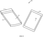
- FIG 2 illustrates parts of an apparatus 200 accommodating multiple antennas according to the present disclosure. Note the parts shown in FIG 2 are provided for illustrative purposes only, and is not mean to limit the scope of the present disclosure. For example, as will be further described hereinbelow with reference to the other figures, disclosure, and the claims, alternative exemplary embodiments may incorporate alternative configurations, e.g., different from what is explicitly shown in FIG 2 .
- FIG 2 components of an apparatus 200, e.g., a mobile phone, are illustrated to highlight certain aspects of the present disclosure.
- a front surface 290 of the apparatus 200 e.g., incorporating a screen 291 (e.g., touch screen or other type of screen) is shown detached from the body 211 of the apparatus 200.
- a substrate 212 Provided at one end, e.g., an upper end or lower end, of the body 211 of the phone is a substrate 212.
- the substrate 212 may be an FR-4 substrate known in the art.
- the substrate 212 may provide supporting structure to hold in place the antenna elements further described hereinbelow.
- the substrate 212 may have a hollow shape, and additional elements (not shown) of the apparatus 200 may be provided in space defined by such hollow shape of the substrate 212.
- the body 211 of the phone further supports a ground plane 210 that may be a flat horizontal conducting surface, and /or substantially physically coextensive with a large surface area of the body 211 of the apparatus 200.
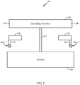
- FIG 3 illustrates an exemplary embodiment of an antenna structure 301 according to the present disclosure.
- the antenna apparatus structure 301 is shown for illustrative purposes only, and is not meant to limit the scope of the present disclosure. It will be appreciated that integration of the elements of the antenna structure 301 with the rest of a wireless device, e.g., the apparatus 200 such as shown in FIG 2 , will be clear to one of ordinary skill in the art in light of the further disclosure hereinbelow, e.g., with reference to FIGs 4-8 .
- the antenna structure 301 includes first and second monopole (antenna) elements 330, 332.
- the first monopole element 330 is coupled by a short conductive strip 331 to a driving terminal, also denoted Port 1 in FIG 3 .
- the second monopole element 332 is coupled by a short conductive strip 333 to a driving terminal Port 0.
- the two monopole elements 330, 332 may have design specifications that are independent of each other, and may correspond to, e.g., a primary antenna and a secondary antenna, respectively. It will be appreciated that the primary and secondary antennas may be driven by, e.g., independent signals, depending on the application.
- the two monopole elements 330, 332 may be partially responsible for the high band radiation of the antenna.
- a primary monopole element may be designed to cover a frequency range of 700-960 MHz and 1710-2170 MHz with a gain of -4dB
- a diversity monopole element may be designed to cover a frequency band of 734-960 MHz and 1805-2170 MHz with a gain of -7dB.
- Each of the monopole elements 330, 332 is capacitively coupled to a common or shared grounding structure 310 (also denoted herein as the "common structure").
- the grounding structure 310 is conductively coupled via a grounding strip 322 (also denoted herein as a “connecting strip") to a ground element (or ground plane) 320.
- the ground plane 320 may correspond to the ground plane 210 in FIG 2 .
- the grounding structure 310, grounding strip 322, and ground element 320 are all conductors, and mutually conductively coupled to each other.
- the common grounding structure 310 may include two branches 310a and 310b, with 310a being in closer physical proximity to first monopole element 330, and 310b being in closer physical proximity to second monopole element 332. Accordingly, branch 310a will be understood as being capacitively coupled to first monopole element 330, while branch 310b will be understood as being capacitively coupled to the second monopole element 332.
- FIG 3 of the grounding structure into two branches 310a and 310b is made for descriptive purposes only. In a practical implementation, no actual physical demarcation need be present between branches 310a, 310b, as it will be appreciated that all portions of the grounding structure 310 are conductively coupled to each other to form a single conductive element.
- the two monopole elements 330, 332 effectively share a single grounding structure 310. It will be appreciated that the increased resonator size decreases the quality factor of the resonance and increases the bandwidth, especially at lower frequencies.
- a "resonator" structure may be defined herein as corresponding to the combination of 330, 322, 310 for Port 1 excitation, and 332, 322, and 310 for Port 2 excitation.
- Providing the shared grounding structure 310 thus advantageously increases the effective size of each monopole antenna, compared to, e.g., alternative implementations wherein a ground structure associated with the first monopole element 330 is physically separated from a ground structure associated with the second monopole element 332. It will be appreciated that increasing the effective size of the monopole antennas improves their radiation performance, while attaining relatively wide bandwidth for both of the monopole elements 330, 332 given the compact physical dimensions of the structure.
- a "one port excitation" scheme may be applied, wherein only one of the two monopole elements 330, 332 is driven at any time.
- one of the monopole elements 330, 332 is driven by an active signal, it is expected that the grounded branch 310a or 310b in closer physical proximity to the driven monopole element will resonate strongly, with weaker coupling to the non-driven monopole element. For example, if Port 1 drives element 330 while Port 2 does not drive element 332, then only the branch 310a of the grounding structure 310 is expected to resonate strongly, while the branch 310b is expected to resonate only weakly.
- the conductive strip 322 coupling the shared grounding structure 310 to the ground plane 320 is provided between the monopole elements 330, 332.
- a "connecting axis" (not shown in FIG 3 ) is defined as connecting a point on the first monopole element 330 with a point on the second monopole element 332, then points on the ground strip 322 will generally have coordinates along such connecting axis that lie between the coordinates corresponding to the first and second monopole elements 330 and 332.
- the grounding structure 310 is large relative to the monopole elements 330, 332, and may additionally shield the monopole elements 330, 332 from, e.g., an external portion of the apparatus 200 (not shown in FIG 2 ).
- the relatively large size of the grounding structure 310 may further protect the input/output signal lines feeding monopole elements 330, 332 through Port 1 and Port 2, respectively, from damage due to electrostatic discharge (ESD).
- ESD electrostatic discharge
- a substrate 212 (not shown in FIG 3 ), e.g., an FR-4 substrate, may be provided in the spacing between the conductive elements of the antenna 301, as mentioned hereinabove with reference to FIG 2 .
- FIG 4 illustrates an exemplary embodiment of an apparatus 400 showing antenna elements integrated with a mobile device according to the present disclosure.
- FIG 4 is shown for illustrative purposes only, and is not meant to limit the scope of the present disclosure. It will be appreciated that certain elements in FIG 4 , and in the rest of the figures, having numerical identifiers in common with elements of FIG 3 may have similar functionality, unless otherwise noted.
- the grounding structure 310.1 in FIG 4 may have similar functionality to that described for the grounding structure 310 in FIG 3 , etc.
- the apparatus 400 with an antenna 301.1 includes first and second monopole elements 330.1, 332.1 driven by Port 1, Port 2, respectively.
- a grounding structure 310.1 is capacitively coupled to both the first and second monopole elements 330.1, 332.1.
- a grounding strip 322.1 conductively couples the grounding structure 310.1 to a ground plane (not labeled in FIG 4 ) of the apparatus 400.
- the monopole elements 330.1, 332.1 are placed on opposite sides Side A and Side B of the apparatus 400. It will be appreciated that such placement of the monopole elements 330.1, 332.1 may advantageously increase their isolation from each other.
- the antenna 301.1 has a clearance to ground (e.g., extent along the Z-axis) of 8.5 mm, a thickness (e.g., extent along the X-axis) of 4.6 mm, and a board width (e.g., extent along the Y-axis) of 68.5 mm. Note the specific dimensions are given for illustrative purposes only, and are not meant to limit the scope of the present disclosure.
- a clearance to ground e.g., extent along the Z-axis
- a thickness e.g., extent along the X-axis
- a board width e.g., extent along the Y-axis
- the exemplary embodiment 400 shows parts of the monopole elements 330.1, 332.1 and the grounding structure 310.1 disposed adjacent a top surface of the apparatus 400 (e.g., a surface closer to the front cover 290 as shown in FIG 2 ), in alternative exemplary embodiments, the monopole elements 330.1, 332.1 and grounding structure 310.1 may readily be disposed adjacent a bottom surface of the apparatus 400 instead. Such alternative exemplary embodiments are contemplated to be within the scope of the present disclosure.
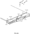
- FIGs 5A and 5B illustrate perspective views of an alternative exemplary embodiment of an antenna 301.2 according to the present disclosure. Note FIGs 5A and 5B are shown for illustrative purposes only, and are not meant to limit the scope of the present disclosure to any specific antenna configuration shown.
- a first monopole element 330.2 is coupled to Port 1
- a second monopole element 332.2 is coupled to Port 2.
- a grounding strip 322.2 couples a ground plane 320.2 to a shared grounding structure 310.2, which is capacitively coupled to both first and second monopole elements 330.2 and 332.2.
- the grounding structure 310.2 includes a first branch 310.2a (capacitively coupled to first monopole element 330.2) conductively coupled to a second branch 310.2b (capacitively coupled to second monopole element 332.2) via a short connecting strip 511.
- the grounding structure 310.2 may extend in multiple dimensions (e.g., along the X-, Y-, and Z-axes), and may be extensively patterned to, e.g., optimize the antenna performance according to the requirements of the design.
- the connecting strip 511 is provided adjacent to the grounding strip 322.2, e.g., the connecting strip 511 and the grounding strip 322.2 have X-coordinates (referring to the X axis as indicated in FIG 5A ) that are relatively close to each other given the overall dimensions of the antenna 301.2. It will be appreciated that the connecting strip 511 conductively couples the two grounding branches 310.2a and 310.2b of the monopole elements to each other, thus enlarging the effective antenna size of each monopole antenna (e.g., wherein each monopole antenna is characterized by the joint size of a monopole element and its associated grounding branch).
- the shape of the first branch 310.2a illustratively includes a patterned formation characterized by, e.g., stubs and lines that capacitively couple to the first monopole element 330.2 along three sides (e.g., along the X-, Y-, and Z-axes).
- the shape of the second branch 310.2b illustratively includes a patterned formation characterized by, e.g., a conductive line that capacitively couples to the second monopole element 332.2 along the Y-axis.
- the shapes of the first branch 310.2a and the second branch 310.2b of the grounding structure 310.2 are shown for illustrative purposes only, and are not meant to limit the scope of the present disclosure.
- the grounding structure 310.2 need not be patterned as illustratively shown in FIGs 5A , 5B , or as shown in other figures herein. Rather, the grounding structure 310.2 may have a simple profile, e.g., a straight rectangular conductive element such as shown in FIG 4 , etc, or any arbitrary profile. Such alternative exemplary embodiments are contemplated to be within the scope of the present disclosure.
- the extremities of the two branches 310.2a, 310.2b away from each other may advantageously result in less coupling between Port 1 and Port 2. Accordingly, the two ends of the grounded branches 310.2a and 310.2b may be provided adjacent opposite sides Side A and Side B of the apparatus 500.
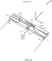
- FIGs 6A , 6B , and 6C illustrate perspective views of an alternative exemplary embodiment of an apparatus 600 incorporating an antenna 301.3 according to the present disclosure. Note FIGs, 6A , 6B , and 6C are shown for illustrative purposes only, and are not meant to limit the scope of the present disclosure.
- a first monopole element 330.3 is coupled to Port 1
- a second monopole element 332.3 is coupled to Port 2.
- a grounding strip 322.3 couples a ground plane 320.3 to a shared grounding structure 310.3, which is capacitively coupled to both first and second monopole elements 330.3 and 332.3.
- the grounding structure 310.3 includes a first branch 310.3a (capacitively coupled to first monopole element 330.3) conductively coupled to a second branch 310.3b (capacitively coupled to second monopole element 332.3) via a short connecting strip 611.
- the connecting strip 611 is provided adjacent to the connection between the grounding strip 322.3 and the shared grounding structure 310.3.
- the patterned shapes of the first branch 310.3a and second branch 310.3b of the grounding structure 310.3 are shown for illustrative purposes only, and are not meant to limit the scope of the present disclosure.
- FIG 6B which shows a perspective view wherein the rear surface of the apparatus 600 is shown facing up (as may be noted from the directionality of the Z the axis shown)
- the grounding element 310.3 includes a relatively large surface 310.3aa that covers the area opposite the first monopole element 330.3 on the bottom side of the substrate 212.
- the grounding element 310.3 includes a relatively large surface 310.3ba that covers the area opposite the second monopole element 332.3 on the bottom side of the substrate 212.
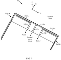
- FIG 7 illustrates an alternative exemplary embodiment of an apparatus 700 incorporating an antenna 301.4.
- a first monopole element 330.4 is coupled to Port 1
- a second monopole element 332.4 is coupled to Port 2.
- a grounding strip 322.4 couples a ground plane 320.4 to a shared grounding structure 310.4, which is capacitively coupled to both first and second monopole elements 330.4 and 332.4.
- the grounding structure 310.4 includes a first branch 310.4a (capacitively coupled to first monopole element 330.4) conductively coupled to a second branch 310.4b (capacitively coupled to second monopole element 332.4).
- connection of first monopole element 330.4 to Port 1 and the connection of second monopole element 332.4 to Port 2 are provided away from the sides (Side A and Side B) of the apparatus 700 housing the antenna 301.4.
- the connections of the monopole elements to Ports 1 or 2 are closer to the grounding strip 322.4 along the Y axis.
- FIG 8 illustrates an alternative exemplary embodiment of the present disclosure, wherein antenna techniques of the present disclosure are integrated with techniques for accommodating additional modules of the apparatus 800.
- FIG 8 is shown for illustrative purposes only, and is not meant to limit the scope of the present disclosure. It will be appreciated that the functionality of certain elements of FIG 8 will be clear in view of the preceding description, and the description of such functionality may accordingly be omitted hereinbelow for ease of discussion.
- apparatus 800 includes an area 810 that would otherwise be occupied by substrate 212 supporting elements of the antenna 301.5.
- the area 810 represents a hollowed-out portion of the substrate 212, wherein additional modules of the apparatus 800 may be provided.
- additional modules of the apparatus 800 may be provided.
- a microphone, speaker, USB connector, etc. may thus be integrated in the same area of the apparatus 800 occupied by the antenna 301.5.
- some degradation in the antenna performance may result when such additional components are inserted into the antenna space in this manner. However, it will be appreciated that such degradation may be tolerated as a design trade-off in certain applications.
- FIG 9 illustrates an exemplary embodiment of a method 900 according to the present disclosure. Note the method 900 is shown for illustrative purposes only, and is not meant to limit the scope of the present disclosure.
- a signal is capacitively coupled from a first monopole element to a first grounded branch.
- a signal is capacitively coupled from a second monopole element to a second grounded branch.
- the first and second branches are capacitively coupled to each other and to a ground element via a single connecting strip disposed between the first and second monopole elements.
- grounding structure 310 e.g., including a relatively short grounding strip 322 and two branches 310a, 310b
- alternative exemplary embodiments may generally adopt any shape for the grounded element that maintains shared capacitive coupling to both the first monopole antenna element 330 and second monopole antenna element 332.
- the branches 310a, 310b have been illustrated as in certain figures herein as including a patterned conductive design, in alternative exemplary embodiments, the patterned designs shown may be replaced by unpatterned shapes, e.g., an unpatterned conducting sheet (e.g., having a simple rectangular shape, etc.). Such alternative exemplary embodiments are contemplated to be within the scope of the present disclosure.
- the techniques of the present disclosure may be applicable to different phone platforms, e.g., 5-inch phones, small phones, thin phones, etc.
- broadband antennas with dimensions of greater or lesser size may be designed according to the techniques disclosed.
- techniques of the present disclosure are not limited to the two-antenna module.
- tri-fed and quad-fed antenna modules may also be designed.
- additional feeding and radiating structures e.g., beyond the two monopole elements described hereinabove
- additional feeding and radiating structures may be provided which nevertheless share a single common grounding structure.
- Such alternative exemplary embodiments are contemplated to be within the scope of the present disclosure.
- DSP Digital Signal Processor
- ASIC Application Specific Integrated Circuit
- FPGA Field Programmable Gate Array
- a general purpose processor may be a microprocessor, but in the alternative, the processor may be any conventional processor, controller, microcontroller, or state machine.
- a processor may also be implemented as a combination of computing devices, e.g., a combination of a DSP and a microprocessor, a plurality of microprocessors, one or more microprocessors in conjunction with a DSP core, or any other such configuration.
- a software module may reside in Random Access Memory (RAM), flash memory, Read Only Memory (ROM), Electrically Programmable ROM (EPROM), Electrically Erasable Programmable ROM (EEPROM), registers, hard disk, a removable disk, a CD-ROM, or any other form of storage medium known in the art.
- An exemplary storage medium is coupled to the processor such that the processor can read information from, and write information to, the storage medium.
- the storage medium may be integral to the processor.
- the processor and the storage medium may reside in an ASIC.
- the ASIC may reside in a user terminal.
- the processor and the storage medium may reside as discrete components in a user terminal.
- the functions described may be implemented in hardware, software, firmware, or any combination thereof. If implemented in software, the functions may be stored on or transmitted over as one or more instructions or code on a computer-readable medium.
- Computer-readable media includes both computer storage media and communication media including any medium that facilitates transfer of a computer program from one place to another.
- a storage media may be any available media that can be accessed by a computer.
- such computer-readable media can comprise RAM, ROM, EEPROM, CD-ROM or other optical disk storage, magnetic disk storage or other magnetic storage devices, or any other medium that can be used to carry or store desired program code in the form of instructions or data structures and that can be accessed by a computer.
- any connection is properly termed a computer-readable medium.
- the software is transmitted from a website, server, or other remote source using a coaxial cable, fiber optic cable, twisted pair, digital subscriber line (DSL), or wireless technologies such as infrared, radio, and microwave
- the coaxial cable, fiber optic cable, twisted pair, DSL, or wireless technologies such as infrared, radio, and microwave are included in the definition of medium.
- Disk and disc includes compact disc (CD), laser disc, optical disc, digital versatile disc (DVD), floppy disk and Blu-Ray disc where disks usually reproduce data magnetically, while discs reproduce data optically with lasers. Combinations of the above should also be included within the scope of computer-readable media.
Landscapes
- Engineering & Computer Science (AREA)
- Computer Networks & Wireless Communication (AREA)
- Details Of Aerials (AREA)
- Variable-Direction Aerials And Aerial Arrays (AREA)
- Support Of Aerials (AREA)
Applications Claiming Priority (2)
| Application Number | Priority Date | Filing Date | Title |
|---|---|---|---|
| US13/932,105 US10044110B2 (en) | 2013-07-01 | 2013-07-01 | Antennas with shared grounding structure |
| PCT/US2014/043017 WO2015002741A1 (en) | 2013-07-01 | 2014-06-18 | Antennas with shared grounding structure |
Publications (2)
| Publication Number | Publication Date |
|---|---|
| EP3017501A1 EP3017501A1 (en) | 2016-05-11 |
| EP3017501B1 true EP3017501B1 (en) | 2018-05-02 |
Family
ID=51134460
Family Applications (1)
| Application Number | Title | Priority Date | Filing Date |
|---|---|---|---|
| EP14736264.4A Active EP3017501B1 (en) | 2013-07-01 | 2014-06-18 | Antennas with shared grounding structure |
Country Status (6)
Families Citing this family (22)
| Publication number | Priority date | Publication date | Assignee | Title |
|---|---|---|---|---|
| US9520650B2 (en) | 2014-03-31 | 2016-12-13 | Intel Corporation | Combination LTE and WiGig antenna |
| TWI539674B (zh) * | 2014-09-26 | 2016-06-21 | 宏碁股份有限公司 | 天線系統 |
| US9755310B2 (en) | 2015-11-20 | 2017-09-05 | Taoglas Limited | Ten-frequency band antenna |
| WO2017142550A1 (en) * | 2016-02-19 | 2017-08-24 | Hewlett-Packard Development Company, L.P. | Integrated antenna |
| JP6778364B2 (ja) * | 2016-03-10 | 2020-11-04 | 大学共同利用機関法人自然科学研究機構 | マイクロ波マンモグラフィ装置 |
| TWM568509U (zh) * | 2018-07-12 | 2018-10-11 | 明泰科技股份有限公司 | 具有低姿勢與雙頻高隔離度之天線模組 |
| CN108987896A (zh) * | 2018-07-27 | 2018-12-11 | 深圳市信维通信股份有限公司 | 一种mimo天线高隔离度终端手机 |
| CN110931973A (zh) * | 2018-09-20 | 2020-03-27 | 中兴通讯股份有限公司 | 终端 |
| US11005184B2 (en) | 2018-11-29 | 2021-05-11 | Samsung Electro-Mechanics Co., Ltd. | Antenna apparatus |
| KR102125085B1 (ko) | 2018-11-29 | 2020-06-19 | 삼성전기주식회사 | 안테나 장치 |
| CN109980364B (zh) * | 2019-02-28 | 2021-09-14 | 华为技术有限公司 | 一种天线模块、天线装置以及终端设备 |
| US11367967B2 (en) | 2019-03-01 | 2022-06-21 | Shenzhen Sunway Communication Co., Ltd. | Compact 5G MIMO antenna system and mobile terminal |
| WO2021065296A1 (ja) * | 2019-10-03 | 2021-04-08 | 株式会社村田製作所 | アンテナ装置およびそれを備えた無線通信デバイス |
| CN112821038A (zh) * | 2019-11-15 | 2021-05-18 | 英业达科技有限公司 | 天线模组 |
| CN110911839B (zh) * | 2019-12-13 | 2020-11-03 | 北京邮电大学 | 一种5g双频带高隔离双端口共地单极子天线 |
| EP4059088B1 (en) | 2019-12-19 | 2025-08-27 | Huawei Technologies Co., Ltd. | Dual polarization connected antenna array |
| CN113224503B (zh) * | 2020-01-21 | 2023-08-04 | 荣耀终端有限公司 | 一种天线及终端设备 |
| CN113764865B (zh) * | 2020-06-02 | 2024-04-05 | 英业达科技有限公司 | 一种天线模块 |
| KR102369732B1 (ko) | 2020-07-08 | 2022-03-02 | 삼성전기주식회사 | 안테나 장치 |
| KR102825633B1 (ko) | 2020-07-31 | 2025-06-26 | 삼성전자주식회사 | 안테나 및 그것을 포함하는 전자 장치 |
| CN112909541B (zh) * | 2021-01-12 | 2023-07-28 | Oppo广东移动通信有限公司 | 天线装置及电子设备 |
| WO2023090498A1 (ko) | 2021-11-22 | 2023-05-25 | 엘지전자 주식회사 | 차량에 배치되는 안테나 모듈 |
Family Cites Families (22)
| Publication number | Priority date | Publication date | Assignee | Title |
|---|---|---|---|---|
| JP2007524310A (ja) | 2004-02-18 | 2007-08-23 | コーニンクレッカ フィリップス エレクトロニクス エヌ ヴィ | アンテナ |
| EP1892798A1 (en) | 2006-08-22 | 2008-02-27 | Matsushita Electric Industrial Co., Ltd. | Folded planar monopole antenna |
| KR101093365B1 (ko) * | 2006-09-27 | 2011-12-14 | 엘지전자 주식회사 | MlMO/Diversity 내장형 안테나 장치 |
| FI120119B (fi) | 2007-01-04 | 2009-06-30 | Pulse Finland Oy | Antennirakenne |
| JP4571988B2 (ja) * | 2007-01-19 | 2010-10-27 | パナソニック株式会社 | アレーアンテナ装置及び無線通信装置 |
| CN101573831B (zh) * | 2007-01-19 | 2012-11-21 | 株式会社村田制作所 | 天线装置及无线通信机 |
| EP2160799A4 (en) * | 2007-03-16 | 2012-05-16 | Tyco Electronics Services Gmbh | METAMATERIAL ANTENNA ARRAYS WITH TORQUE SHAPING AND BEAM SWITCHING |
| TWI396331B (zh) * | 2007-04-17 | 2013-05-11 | Quanta Comp Inc | Dual frequency antenna |
| KR100951582B1 (ko) * | 2007-11-02 | 2010-04-09 | 한양대학교 산학협력단 | 초광대역 다이버시티 안테나 |
| JP5163262B2 (ja) * | 2008-04-30 | 2013-03-13 | 富士通セミコンダクター株式会社 | アンテナ及びそのアンテナを有する通信装置 |
| WO2010028521A1 (en) | 2008-09-11 | 2010-03-18 | Hong Kong Applied Science And Technology Research Institute Co., Ltd. | Systems and methods employing coupling elements to increase antenna isolation |
| US20100069117A1 (en) * | 2008-09-18 | 2010-03-18 | Knighton Mark S | USB enabled mobile phone handset |
| TWI423521B (zh) | 2009-10-26 | 2014-01-11 | Acer Inc | 多頻行動通訊裝置及其天線 |
| WO2011103327A1 (en) * | 2010-02-17 | 2011-08-25 | Rftelligent, Inc. | Field-confined printed circuit board-printed antenna for radio frequency front end integrated circuits |
| TWI450441B (zh) | 2011-02-25 | 2014-08-21 | Acer Inc | 行動通訊裝置及其天線結構 |
| CN102804496B (zh) | 2011-03-16 | 2014-05-07 | 松下电器产业株式会社 | 天线装置 |
| US9024823B2 (en) * | 2011-05-27 | 2015-05-05 | Apple Inc. | Dynamically adjustable antenna supporting multiple antenna modes |
| US9306276B2 (en) | 2011-07-13 | 2016-04-05 | Qualcomm Incorporated | Wideband antenna system with multiple antennas and at least one parasitic element |
| US8854266B2 (en) | 2011-08-23 | 2014-10-07 | Apple Inc. | Antenna isolation elements |
| KR101293660B1 (ko) | 2011-08-29 | 2013-08-13 | 엘에스엠트론 주식회사 | 높은 격리도를 갖는 미모/다이버시티 안테나 |
| WO2013077302A1 (ja) | 2011-11-25 | 2013-05-30 | 株式会社村田製作所 | アンテナ装置および電子機器 |
| JP5404882B1 (ja) | 2012-09-26 | 2014-02-05 | 株式会社東芝 | アンテナ装置とこのアンテナ装置を備えた電子機器 |
-
2013
- 2013-07-01 US US13/932,105 patent/US10044110B2/en active Active
-
2014
- 2014-06-18 CN CN201480037904.XA patent/CN105379008B/zh active Active
- 2014-06-18 KR KR1020167002167A patent/KR102150631B1/ko active Active
- 2014-06-18 EP EP14736264.4A patent/EP3017501B1/en active Active
- 2014-06-18 WO PCT/US2014/043017 patent/WO2015002741A1/en active Application Filing
- 2014-06-18 JP JP2016523801A patent/JP6396450B2/ja active Active
Non-Patent Citations (1)
| Title |
|---|
| None * |
Also Published As
| Publication number | Publication date |
|---|---|
| EP3017501A1 (en) | 2016-05-11 |
| JP2016524427A (ja) | 2016-08-12 |
| CN105379008B (zh) | 2021-03-12 |
| KR20160025582A (ko) | 2016-03-08 |
| US20150002359A1 (en) | 2015-01-01 |
| CN105379008A (zh) | 2016-03-02 |
| WO2015002741A1 (en) | 2015-01-08 |
| KR102150631B1 (ko) | 2020-09-01 |
| JP6396450B2 (ja) | 2018-09-26 |
| US10044110B2 (en) | 2018-08-07 |
Similar Documents
| Publication | Publication Date | Title |
|---|---|---|
| EP3017501B1 (en) | Antennas with shared grounding structure | |
| US7450072B2 (en) | Modified inverted-F antenna for wireless communication | |
| CN108461902B (zh) | 三宽带混合lte隙缝天线 | |
| US8711043B2 (en) | Wideband antenna | |
| EP3767742B1 (en) | Antenna device and mobile terminal | |
| US7411554B2 (en) | MIMO antenna operable in multiband | |
| CN101336497B (zh) | 四波段耦合元件天线结构 | |
| WO2019161315A1 (en) | Multi-band wireless signaling | |
| US20200106178A1 (en) | Antenna system | |
| US9825366B2 (en) | Printed circuit board antenna and printed circuit board | |
| CN103178358A (zh) | 可切换的分集天线设备和方法 | |
| US20110210898A1 (en) | Ground radiation antenna | |
| KR20120054084A (ko) | 고절연 안테나 시스템 | |
| CN108808222A (zh) | 天线系统及电子设备 | |
| US20140320379A1 (en) | Antenna apparatus capable of reducing decreases in gain and bandwidth | |
| US20130057446A1 (en) | Antenna device and portable wireless terminal equipped with the same | |
| CN116345145B (zh) | 可折叠电子设备及其天线系统 | |
| US9331398B2 (en) | Dual-mode terminal antenna and signal processing method | |
| CN105789836A (zh) | 天线系统和移动终端 | |
| US7123209B1 (en) | Low-profile, multi-frequency, differential antenna structures | |
| CN105428807A (zh) | 一种多模缝隙天线和移动终端 | |
| CA2803642C (en) | Mobile wireless communications device with multiple-band antenna and related methods | |
| US20110193762A1 (en) | Ground radiation antenna | |
| CN103219589A (zh) | 对安装在印刷电路板上的天线隔离的改进 | |
| US10205217B2 (en) | Antenna for wireless communication device chassis having reduced cutback |
Legal Events
| Date | Code | Title | Description |
|---|---|---|---|
| PUAI | Public reference made under article 153(3) epc to a published international application that has entered the european phase |
Free format text: ORIGINAL CODE: 0009012 |
|
| 17P | Request for examination filed |
Effective date: 20151117 |
|
| AK | Designated contracting states |
Kind code of ref document: A1 Designated state(s): AL AT BE BG CH CY CZ DE DK EE ES FI FR GB GR HR HU IE IS IT LI LT LU LV MC MK MT NL NO PL PT RO RS SE SI SK SM TR |
|
| AX | Request for extension of the european patent |
Extension state: BA ME |
|
| DAX | Request for extension of the european patent (deleted) | ||
| GRAP | Despatch of communication of intention to grant a patent |
Free format text: ORIGINAL CODE: EPIDOSNIGR1 |
|
| INTG | Intention to grant announced |
Effective date: 20170629 |
|
| GRAS | Grant fee paid |
Free format text: ORIGINAL CODE: EPIDOSNIGR3 |
|
| GRAJ | Information related to disapproval of communication of intention to grant by the applicant or resumption of examination proceedings by the epo deleted |
Free format text: ORIGINAL CODE: EPIDOSDIGR1 |
|
| GRAL | Information related to payment of fee for publishing/printing deleted |
Free format text: ORIGINAL CODE: EPIDOSDIGR3 |
|
| GRAP | Despatch of communication of intention to grant a patent |
Free format text: ORIGINAL CODE: EPIDOSNIGR1 |
|
| INTC | Intention to grant announced (deleted) | ||
| INTG | Intention to grant announced |
Effective date: 20171130 |
|
| GRAA | (expected) grant |
Free format text: ORIGINAL CODE: 0009210 |
|
| AK | Designated contracting states |
Kind code of ref document: B1 Designated state(s): AL AT BE BG CH CY CZ DE DK EE ES FI FR GB GR HR HU IE IS IT LI LT LU LV MC MK MT NL NO PL PT RO RS SE SI SK SM TR |
|
| REG | Reference to a national code |
Ref country code: GB Ref legal event code: FG4D |
|
| REG | Reference to a national code |
Ref country code: FR Ref legal event code: PLFP Year of fee payment: 5 |
|
| REG | Reference to a national code |
Ref country code: CH Ref legal event code: EP Ref country code: AT Ref legal event code: REF Ref document number: 996233 Country of ref document: AT Kind code of ref document: T Effective date: 20180515 |
|
| REG | Reference to a national code |
Ref country code: DE Ref legal event code: R096 Ref document number: 602014024864 Country of ref document: DE Ref country code: IE Ref legal event code: FG4D |
|
| REG | Reference to a national code |
Ref country code: DE Ref legal event code: R096 Ref document number: 602014024864 Country of ref document: DE |
|
| REG | Reference to a national code |
Ref country code: NL Ref legal event code: MP Effective date: 20180502 |
|
| REG | Reference to a national code |
Ref country code: LT Ref legal event code: MG4D |
|
| PG25 | Lapsed in a contracting state [announced via postgrant information from national office to epo] |
Ref country code: ES Free format text: LAPSE BECAUSE OF FAILURE TO SUBMIT A TRANSLATION OF THE DESCRIPTION OR TO PAY THE FEE WITHIN THE PRESCRIBED TIME-LIMIT Effective date: 20180502 Ref country code: BG Free format text: LAPSE BECAUSE OF FAILURE TO SUBMIT A TRANSLATION OF THE DESCRIPTION OR TO PAY THE FEE WITHIN THE PRESCRIBED TIME-LIMIT Effective date: 20180802 Ref country code: LT Free format text: LAPSE BECAUSE OF FAILURE TO SUBMIT A TRANSLATION OF THE DESCRIPTION OR TO PAY THE FEE WITHIN THE PRESCRIBED TIME-LIMIT Effective date: 20180502 Ref country code: NO Free format text: LAPSE BECAUSE OF FAILURE TO SUBMIT A TRANSLATION OF THE DESCRIPTION OR TO PAY THE FEE WITHIN THE PRESCRIBED TIME-LIMIT Effective date: 20180802 Ref country code: FI Free format text: LAPSE BECAUSE OF FAILURE TO SUBMIT A TRANSLATION OF THE DESCRIPTION OR TO PAY THE FEE WITHIN THE PRESCRIBED TIME-LIMIT Effective date: 20180502 Ref country code: SE Free format text: LAPSE BECAUSE OF FAILURE TO SUBMIT A TRANSLATION OF THE DESCRIPTION OR TO PAY THE FEE WITHIN THE PRESCRIBED TIME-LIMIT Effective date: 20180502 |
|
| PG25 | Lapsed in a contracting state [announced via postgrant information from national office to epo] |
Ref country code: LV Free format text: LAPSE BECAUSE OF FAILURE TO SUBMIT A TRANSLATION OF THE DESCRIPTION OR TO PAY THE FEE WITHIN THE PRESCRIBED TIME-LIMIT Effective date: 20180502 Ref country code: HR Free format text: LAPSE BECAUSE OF FAILURE TO SUBMIT A TRANSLATION OF THE DESCRIPTION OR TO PAY THE FEE WITHIN THE PRESCRIBED TIME-LIMIT Effective date: 20180502 Ref country code: GR Free format text: LAPSE BECAUSE OF FAILURE TO SUBMIT A TRANSLATION OF THE DESCRIPTION OR TO PAY THE FEE WITHIN THE PRESCRIBED TIME-LIMIT Effective date: 20180803 Ref country code: NL Free format text: LAPSE BECAUSE OF FAILURE TO SUBMIT A TRANSLATION OF THE DESCRIPTION OR TO PAY THE FEE WITHIN THE PRESCRIBED TIME-LIMIT Effective date: 20180502 Ref country code: RS Free format text: LAPSE BECAUSE OF FAILURE TO SUBMIT A TRANSLATION OF THE DESCRIPTION OR TO PAY THE FEE WITHIN THE PRESCRIBED TIME-LIMIT Effective date: 20180502 |
|
| REG | Reference to a national code |
Ref country code: AT Ref legal event code: MK05 Ref document number: 996233 Country of ref document: AT Kind code of ref document: T Effective date: 20180502 |
|
| PG25 | Lapsed in a contracting state [announced via postgrant information from national office to epo] |
Ref country code: CZ Free format text: LAPSE BECAUSE OF FAILURE TO SUBMIT A TRANSLATION OF THE DESCRIPTION OR TO PAY THE FEE WITHIN THE PRESCRIBED TIME-LIMIT Effective date: 20180502 Ref country code: SK Free format text: LAPSE BECAUSE OF FAILURE TO SUBMIT A TRANSLATION OF THE DESCRIPTION OR TO PAY THE FEE WITHIN THE PRESCRIBED TIME-LIMIT Effective date: 20180502 Ref country code: RO Free format text: LAPSE BECAUSE OF FAILURE TO SUBMIT A TRANSLATION OF THE DESCRIPTION OR TO PAY THE FEE WITHIN THE PRESCRIBED TIME-LIMIT Effective date: 20180502 Ref country code: PL Free format text: LAPSE BECAUSE OF FAILURE TO SUBMIT A TRANSLATION OF THE DESCRIPTION OR TO PAY THE FEE WITHIN THE PRESCRIBED TIME-LIMIT Effective date: 20180502 Ref country code: AT Free format text: LAPSE BECAUSE OF FAILURE TO SUBMIT A TRANSLATION OF THE DESCRIPTION OR TO PAY THE FEE WITHIN THE PRESCRIBED TIME-LIMIT Effective date: 20180502 Ref country code: DK Free format text: LAPSE BECAUSE OF FAILURE TO SUBMIT A TRANSLATION OF THE DESCRIPTION OR TO PAY THE FEE WITHIN THE PRESCRIBED TIME-LIMIT Effective date: 20180502 Ref country code: EE Free format text: LAPSE BECAUSE OF FAILURE TO SUBMIT A TRANSLATION OF THE DESCRIPTION OR TO PAY THE FEE WITHIN THE PRESCRIBED TIME-LIMIT Effective date: 20180502 |
|
| REG | Reference to a national code |
Ref country code: CH Ref legal event code: PL |
|
| REG | Reference to a national code |
Ref country code: DE Ref legal event code: R097 Ref document number: 602014024864 Country of ref document: DE |
|
| PG25 | Lapsed in a contracting state [announced via postgrant information from national office to epo] |
Ref country code: IT Free format text: LAPSE BECAUSE OF FAILURE TO SUBMIT A TRANSLATION OF THE DESCRIPTION OR TO PAY THE FEE WITHIN THE PRESCRIBED TIME-LIMIT Effective date: 20180502 Ref country code: SM Free format text: LAPSE BECAUSE OF FAILURE TO SUBMIT A TRANSLATION OF THE DESCRIPTION OR TO PAY THE FEE WITHIN THE PRESCRIBED TIME-LIMIT Effective date: 20180502 |
|
| REG | Reference to a national code |
Ref country code: BE Ref legal event code: MM Effective date: 20180630 |
|
| PLBE | No opposition filed within time limit |
Free format text: ORIGINAL CODE: 0009261 |
|
| STAA | Information on the status of an ep patent application or granted ep patent |
Free format text: STATUS: NO OPPOSITION FILED WITHIN TIME LIMIT |
|
| REG | Reference to a national code |
Ref country code: IE Ref legal event code: MM4A |
|
| PG25 | Lapsed in a contracting state [announced via postgrant information from national office to epo] |
Ref country code: LU Free format text: LAPSE BECAUSE OF NON-PAYMENT OF DUE FEES Effective date: 20180618 Ref country code: MC Free format text: LAPSE BECAUSE OF FAILURE TO SUBMIT A TRANSLATION OF THE DESCRIPTION OR TO PAY THE FEE WITHIN THE PRESCRIBED TIME-LIMIT Effective date: 20180502 |
|
| 26N | No opposition filed |
Effective date: 20190205 |
|
| PG25 | Lapsed in a contracting state [announced via postgrant information from national office to epo] |
Ref country code: CH Free format text: LAPSE BECAUSE OF NON-PAYMENT OF DUE FEES Effective date: 20180630 Ref country code: LI Free format text: LAPSE BECAUSE OF NON-PAYMENT OF DUE FEES Effective date: 20180630 Ref country code: IE Free format text: LAPSE BECAUSE OF NON-PAYMENT OF DUE FEES Effective date: 20180618 |
|
| PG25 | Lapsed in a contracting state [announced via postgrant information from national office to epo] |
Ref country code: BE Free format text: LAPSE BECAUSE OF NON-PAYMENT OF DUE FEES Effective date: 20180630 Ref country code: SI Free format text: LAPSE BECAUSE OF FAILURE TO SUBMIT A TRANSLATION OF THE DESCRIPTION OR TO PAY THE FEE WITHIN THE PRESCRIBED TIME-LIMIT Effective date: 20180502 |
|
| PG25 | Lapsed in a contracting state [announced via postgrant information from national office to epo] |
Ref country code: AL Free format text: LAPSE BECAUSE OF FAILURE TO SUBMIT A TRANSLATION OF THE DESCRIPTION OR TO PAY THE FEE WITHIN THE PRESCRIBED TIME-LIMIT Effective date: 20180502 |
|
| PG25 | Lapsed in a contracting state [announced via postgrant information from national office to epo] |
Ref country code: MT Free format text: LAPSE BECAUSE OF NON-PAYMENT OF DUE FEES Effective date: 20180618 |
|
| PG25 | Lapsed in a contracting state [announced via postgrant information from national office to epo] |
Ref country code: TR Free format text: LAPSE BECAUSE OF FAILURE TO SUBMIT A TRANSLATION OF THE DESCRIPTION OR TO PAY THE FEE WITHIN THE PRESCRIBED TIME-LIMIT Effective date: 20180502 |
|
| PG25 | Lapsed in a contracting state [announced via postgrant information from national office to epo] |
Ref country code: PT Free format text: LAPSE BECAUSE OF FAILURE TO SUBMIT A TRANSLATION OF THE DESCRIPTION OR TO PAY THE FEE WITHIN THE PRESCRIBED TIME-LIMIT Effective date: 20180502 |
|
| PG25 | Lapsed in a contracting state [announced via postgrant information from national office to epo] |
Ref country code: HU Free format text: LAPSE BECAUSE OF FAILURE TO SUBMIT A TRANSLATION OF THE DESCRIPTION OR TO PAY THE FEE WITHIN THE PRESCRIBED TIME-LIMIT; INVALID AB INITIO Effective date: 20140618 Ref country code: MK Free format text: LAPSE BECAUSE OF NON-PAYMENT OF DUE FEES Effective date: 20180502 Ref country code: CY Free format text: LAPSE BECAUSE OF FAILURE TO SUBMIT A TRANSLATION OF THE DESCRIPTION OR TO PAY THE FEE WITHIN THE PRESCRIBED TIME-LIMIT Effective date: 20180502 |
|
| PG25 | Lapsed in a contracting state [announced via postgrant information from national office to epo] |
Ref country code: IS Free format text: LAPSE BECAUSE OF FAILURE TO SUBMIT A TRANSLATION OF THE DESCRIPTION OR TO PAY THE FEE WITHIN THE PRESCRIBED TIME-LIMIT Effective date: 20180902 |
|
| PGFP | Annual fee paid to national office [announced via postgrant information from national office to epo] |
Ref country code: GB Payment date: 20240509 Year of fee payment: 11 |
|
| PGFP | Annual fee paid to national office [announced via postgrant information from national office to epo] |
Ref country code: DE Payment date: 20240509 Year of fee payment: 11 |
|
| PGFP | Annual fee paid to national office [announced via postgrant information from national office to epo] |
Ref country code: FR Payment date: 20240509 Year of fee payment: 11 |