EP3016154A1 - Led device - Google Patents
Led device Download PDFInfo
- Publication number
- EP3016154A1 EP3016154A1 EP14817164.8A EP14817164A EP3016154A1 EP 3016154 A1 EP3016154 A1 EP 3016154A1 EP 14817164 A EP14817164 A EP 14817164A EP 3016154 A1 EP3016154 A1 EP 3016154A1
- Authority
- EP
- European Patent Office
- Prior art keywords
- led device
- led
- frame
- electrode
- shaped electrode
- Prior art date
- Legal status (The legal status is an assumption and is not a legal conclusion. Google has not performed a legal analysis and makes no representation as to the accuracy of the status listed.)
- Granted
Links
Images







Classifications
-
- H—ELECTRICITY
- H10—SEMICONDUCTOR DEVICES; ELECTRIC SOLID-STATE DEVICES NOT OTHERWISE PROVIDED FOR
- H10H—INORGANIC LIGHT-EMITTING SEMICONDUCTOR DEVICES HAVING POTENTIAL BARRIERS
- H10H20/00—Individual inorganic light-emitting semiconductor devices having potential barriers, e.g. light-emitting diodes [LED]
- H10H20/80—Constructional details
- H10H20/85—Packages
- H10H20/857—Interconnections, e.g. lead-frames, bond wires or solder balls
-
- H—ELECTRICITY
- H10—SEMICONDUCTOR DEVICES; ELECTRIC SOLID-STATE DEVICES NOT OTHERWISE PROVIDED FOR
- H10H—INORGANIC LIGHT-EMITTING SEMICONDUCTOR DEVICES HAVING POTENTIAL BARRIERS
- H10H20/00—Individual inorganic light-emitting semiconductor devices having potential barriers, e.g. light-emitting diodes [LED]
- H10H20/80—Constructional details
- H10H20/83—Electrodes
- H10H20/831—Electrodes characterised by their shape
- H10H20/8316—Multi-layer electrodes comprising at least one discontinuous layer
-
- H—ELECTRICITY
- H10—SEMICONDUCTOR DEVICES; ELECTRIC SOLID-STATE DEVICES NOT OTHERWISE PROVIDED FOR
- H10H—INORGANIC LIGHT-EMITTING SEMICONDUCTOR DEVICES HAVING POTENTIAL BARRIERS
- H10H20/00—Individual inorganic light-emitting semiconductor devices having potential barriers, e.g. light-emitting diodes [LED]
- H10H20/80—Constructional details
- H10H20/85—Packages
- H10H20/8506—Containers
-
- H—ELECTRICITY
- H10—SEMICONDUCTOR DEVICES; ELECTRIC SOLID-STATE DEVICES NOT OTHERWISE PROVIDED FOR
- H10H—INORGANIC LIGHT-EMITTING SEMICONDUCTOR DEVICES HAVING POTENTIAL BARRIERS
- H10H29/00—Integrated devices, or assemblies of multiple devices, comprising at least one light-emitting semiconductor element covered by group H10H20/00
- H10H29/10—Integrated devices comprising at least one light-emitting semiconductor component covered by group H10H20/00
- H10H29/14—Integrated devices comprising at least one light-emitting semiconductor component covered by group H10H20/00 comprising multiple light-emitting semiconductor components
- H10H29/142—Two-dimensional arrangements, e.g. asymmetric LED layout
-
- H—ELECTRICITY
- H10—SEMICONDUCTOR DEVICES; ELECTRIC SOLID-STATE DEVICES NOT OTHERWISE PROVIDED FOR
- H10H—INORGANIC LIGHT-EMITTING SEMICONDUCTOR DEVICES HAVING POTENTIAL BARRIERS
- H10H20/00—Individual inorganic light-emitting semiconductor devices having potential barriers, e.g. light-emitting diodes [LED]
- H10H20/80—Constructional details
- H10H20/84—Coatings, e.g. passivation layers or antireflective coatings
- H10H20/841—Reflective coatings, e.g. dielectric Bragg reflectors
-
- H—ELECTRICITY
- H10—SEMICONDUCTOR DEVICES; ELECTRIC SOLID-STATE DEVICES NOT OTHERWISE PROVIDED FOR
- H10W—GENERIC PACKAGES, INTERCONNECTIONS, CONNECTORS OR OTHER CONSTRUCTIONAL DETAILS OF DEVICES COVERED BY CLASS H10
- H10W90/00—Package configurations
- H10W90/701—Package configurations characterised by the relative positions of pads or connectors relative to package parts
- H10W90/751—Package configurations characterised by the relative positions of pads or connectors relative to package parts of bond wires
- H10W90/754—Package configurations characterised by the relative positions of pads or connectors relative to package parts of bond wires between a chip and a stacked insulating package substrate, interposer or RDL
Definitions
- the present invention relates to an LED device.
- An LED device in which an LED in a bare chip state (hereinafter, also referred to as an LED die) is mounted onto a submount substrate and which is packaged by coating with a resin or the like.
- the submount substrate is a small-sized substrate that is inserted between the LED die and a large-sized substrate (hereinafter, also referred to as a mother substrate) on which other electronic parts, such as resistors capacitors, are mounted, and the submount substrate is also referred to as an interposer.
- the submount substrate includes an anode electrode and a cathode electrode on the bottom in opposition to the surface of the mother substrate (e.g., see Patent Document 1).
- FIG. 14 is a perspective view of a conventional semiconductor package corresponding to FIG. 1 of Patent Document 1
- FIG. 15 is a bottom view of a conventional semiconductor package corresponding to FIG. 4 of Patent Document 1.
- An LED device (semiconductor package) 20 has a submount substrate (wire substrate) 10 and an LED die (LED element) 61 flip-chip-mounted on the submount substrate. Bumps 61a and 61b joined to the cathode electrode and the anode electrode, respectively, of the LED die are provided on the bottom of the LED die 61.
- the submount substrate 10 has a ceramic substrate 11 and a pair of electrodes 12 and 13 arranged on the ceramic substrate 11. Each of the pair of electrodes 12 and 13 has surface electrodes 12a and 13a, side electrodes 12b and 13b (not illustrated), and bottom electrodes 12c and 13c and those electrodes function as the anode electrode and the cathode electrode of the LED device 20.
- the LED die 61 is joined to land portions that are formed on the surface electrodes 12a and 13a, respectively, of the pair of electrodes 12 and 13 via the bumps 61a and 61b.
- pairs of recesses 11a and 11b and vias 11c and 11d are formed in the submount substrate 10.
- the side electrodes 12b and 13b are arranged in the pair of recesses 11a and 11b, and the vias 11c and 11d conduct heat generated in the LED die 61 from the surface of the submount substrate to the bottom.
- the bottom electrodes 12c and 13c having identical shapes and the identical areas are arranged on the bottom of the LED device 20.
- the size and spacing of the upper-side electrodes 12a and 12b are determined by the electrode specifications (design rules, mounting accuracy, etc.) of the LED die 61, whereas the size and spacing of the bottom electrodes 12c and 13c are determined by the mounting specifications of the mother substrate.
- Patent Document 1 Japanese Laid Open Patent Document No. 2005-191097 ( FIGs. 1 and 4 )
- the bottom of the conventional LED device (semiconductor package) 20 illustrated in FIG. 14 may be stained, if a liquid is attached to the mother substrate on which the LED device is mounted when the LED device is mounted on the mother substrate. Foreign matter, such as a liquid, which is attached to the bottom of the LED device may cause migration and a short circuit between the electrodes of the LED device.
- the object of present invention is to solve the above problem, i.e., to provide an LED device whose bottom is not stained, even if foreign matter, such as a liquid, is attached.
- the LED device of the present invention has an LED die, a submount substrate on the surface of which the LED die is mounted, a frame-shaped electrode arranged along the periphery of the bottom of the submount substrate, and an inside electrode surrounded by the frame-shaped electrode and connected to the electrode of the LED die.
- the frame-shaped electrode and the inside electrode are connected to the wire electrode on the mother substrate by solder.
- Solder used to join the frame-shaped electrode to the mother substrate exists along the periphery of the bottom of the submount substrate that forms the bottom of the LED device, and therefore the sides along which the frame-shaped electrode is arranged on the bottom of the submount substrate are sealed.
- foreign matter such as a liquid, no longer invades the bottom of the LED device through the sides along which the frame-shaped electrode is arranged.
- the frame-shaped electrode may be arranged across the entire periphery of the bottom.
- the shape of the bottom is rectangular and the frame-shaped electrode may be arranged along the three sides of the bottom.
- the frame-shaped electrode may be connected to the electrode of the LED die.
- the frame-shaped electrode may be connected to the ground wire that is formed on the mother substrate on which the LED device is mounted.
- the LED device of the present invention may have at least two inside electrodes.
- the LED dies may be a red light-emitting LED die, a green light-emitting LED die, and a blue light-emitting LED die.
- the LED device of the present invention includes a frame-shaped electrode that is arranged along the periphery of the bottom, and therefore the bottom of the LED device may be prevented from being stained by sealing the sides along which the frame-shaped electrode is arranged on the bottom of the LED device that is mounted on the mother substrate.
- FIG. 1 is a perspective view of an LED device 1 of a first embodiment.
- the LED device 1 has a reflection layer 2 that is arranged on the uppermost part, a phosphor layer 3 that is arranged beneath the reflection layer 2, a submount substrate 4 that is arranged beneath the phosphor layer 3, and a frame-shaped electrode 5 that is arranged beneath the submount substrate 4.
- FIG. 2 is a perspective view illustrating the state where the LED device 1 of the first embodiment is mounted on a mother substrate 7.
- the LED device 1 is connected to a wire electrode, not illustrated, which is formed on the mother substrate 7, by solder 6.
- the solder 6 forms a fillet and surrounds the LED device 1.
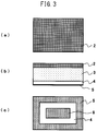
- FIGs. 3A to 3C are external views of the LED device 1 of the first embodiment and FIG. 3A is a plan view of the LED device 1, FIG. 3B is a front view of the LED device 1, and FIG. 3C is a bottom view of the LED device 1.
- the reflection layer 2 is seen from the surface direction of the LED device 1.
- the frame-shaped electrode 5, the submount substrate 4 on which the frame-shaped electrode 5 is formed, and the phosphor layer 3 and the reflection layer 2 stacked on the submount substrate 4, respectively, are seen from the front direction of the LED device 1.
- the frame-shaped electrode 5 that is formed and arranged so as to surround the periphery of the bottom of the submount substrate 4, and an inside electrode 8 that is surrounded by the frame-shaped electrode 5 are seen from the bottom direction of the LED device 1.
- the bottom of the submount substrate 4 is seen between the frame-shaped electrode 5 and the inside electrode 8.
- FIG. 4 is a section view along AA line in FIG. 2 .
- Surface electrodes 4a and 4b are formed on the surface of the submount substrate 4, and through holes 4c and 4d that penetrate through from the surface to the bottom are formed in the submount substrate 4.
- the surface electrode 4a is connected to the frame-shaped electrode 5 via the through hole 4c, and the surface electrode 4b is connected to the inside electrode 8 via the through hole 4d.
- An LED die 9 is die-bonded to the surface of the surface electrode 4b.
- a wire 9a connects the electrode of the LED die 9 and the surface electrodes 4a and 4b.
- the LED die 9 and the wire 9a are coated by the phosphor layer 3.
- the reflection layer 2 is arranged on the phosphor layer 3.
- Wire electrodes 7a and 7b are formed on the surface of the mother substrate 7.
- the wire electrode 7a is connected to the frame-shaped electrode 5 via the solder 6 and the wire electrode 7b is connected to the inside electrode 8 via the solder 6.
- the material that forms the submount substrate 4 is selected from among insulting materials whose thermal conductivity is high.
- alumina whose thermal conductivity is excellent and whose reflectance is high is used as the material that forms the submount substrate 4.
- aluminum nitride whose reflectance is low and whose thermal conductivity is high may be used as the material that forms the submount substrate 4.
- a resin or a metal substrate whose surface has been subjected to insulation processing may be used as the material of the submount substrate 4.
- Each of the surface electrodes 4a and 4b, the frame-shaped electrode 5, and the inside electrode 8 is formed by stacking Ni and Au on Cu.
- the hollow part of the through holes 4c and 4d is filled with an electrically conductive member, such as cupper paste.
- the LED die 9 is a blue light-emitting diode and includes a sapphire substrate and a semiconductor layer that is stacked on the sapphire.
- the thickness of the sapphire substrate is about 150 ⁇ m and the thickness of the semiconductor layer is slightly less than 10 ⁇ m.
- the semiconductor layer includes an n-type GaN layer and a p-type GaN layer that is stacked on the n-type GaN layer, and the boundary part between the n-type GaN layer and the p-type GaN layer functions as a light-emitting layer. Further, the n-type GaN layer is connected to the cathode of the LED die 9 and the p-type GaN layer is connected to the anode of the LED die 9.
- the phosphor layer 3 is formed by curing silicone kneaded with phosphor.
- the reflection layer 2 is formed by curing silicone kneaded with alumina or titanium oxide.
- the reflection layer 2 may be a metal plate or a reflecting tape. Light emitted from the LED die 9 is reflected from the surface of the submount substrate 4 and from the reflection layer 2, and is emitted from the side of the LED device 1 after propagating through the phosphor layer 3. Part of the light that is emitted from the LED die 9 is wavelength-converted by the phosphor included in the phosphor layer 3.
- the frame-shaped electrode 5 is connected to one of the electrodes of the anode and the cathode of the LED die 9, and the inside electrode 8 is connected to the other electrode of the anode and the cathode.
- the inside electrode 8 is connected to the other electrode of the anode and the cathode.
- the frame-shaped electrode may be connected to neither the anode nor the cathode.
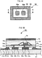
- FIG. 5A is a bottom view of the LED device 50 of the second embodiment and FIG. 5B is a section view along AA line in FIG. 5A .
- An LED die 59, a phosphor layer 53, and a reflection layer 52 are arranged on a submount substrate 54 in the LED device 50, as in the LED device 1 of the first embodiment.
- a perspective view illustrating the external view of the LED device 50 is not provided (regarding embodiments to be explained below, a perspective view illustrating the external view is not provided).
- a frame-shaped electrode 55 is arranged on the periphery of the bottom of the LED device 50, and two inside electrodes 58a and 58b are arranged inside the frame-shaped electrode 55.
- the frame-shaped electrode 55 is connected to a ground wire 57a of a mother substrate 57, and the frame-shaped electrode 55 is not connected to the LED die 59 that is mounted on the submount substrate 54.
- the inside electrode 58a is connected to the anode of the LED device 59 via a through hole 54d, a surface electrode 54a, and a wire.
- the inside electrode 58b is connected to the cathode of the LED die 59 via a through hole 54c, a surface electrode 54b, and a wire 59a.
- the LED device 50 When the LED device 50 is mounted on the mother substrate 57, since the voltage level of the frame-shaped electrode 55 that is formed on the periphery of the bottom is the ground level, and the frame-shaped electrode 55 is not connected to the LED die 59, static electricity may not affect the LED device 50.
- one LED die (the LED die 9 in the LED device 1 (see FIG. 4 )) is mounted on the submount substrates 4 and 54.
- the number of LED dies that are mounted on the submount substrate is not limited to one.
- an LED device 60 in which three LED dies are mounted on a submount substrate 64 is explained as a third embodiment.
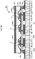
- FIG. 6A is a bottom view of the LED device 60
- FIG. 6B is a section view along AA line in FIG. 6A
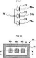
- FIG. 7 is a circuit diagram of the LED device 60.
- LED dies 71, 72, and 73, a phosphor layer 63, and a reflection layer 62 are arranged on the submount substrate 64.
- a frame-shaped electrode 65 is arranged on the periphery of the bottom of the LED device 60, and three inside electrodes 68a, 68b, and 68c are arranged inside the frame-shaped electrode 65.
- the three inside electrodes 68a, 68b, and 68c are arranged so as to form an isosceles triangle in which the inside electrode 68a is located at the vertex and the inside electrodes 68b and 68c form the base.
- the frame-shaped electrode 65 is a common electrode that is connected to the anode of each of the LED dies 71, 72, and 73 and the inside electrodes 68a, 68b, and 68c are connected to cathodes 78a, 78b, and 78c of the LED dies 71, 72, and 73, respectively.
- the LED dies 71, 72, and 73 are a red light-emitting diode, a green light-emitting diode, and a blue light-emitting diode, respectively.
- the LED dies 71, 72, and 73 share an anode 75, and include the cathodes 78a, 78b, and 78c, respectively.
- the anode 75 of the LED dies 71, 72, and 73 is connected to the frame-shaped electrode 65 via a wire 69a, a surface electrode 64a, and a through hole 64c.
- the cathodes 78a, 78b, and 78c of the LED dies 71, 72, and 73 are connected to the inside electrodes 68a, 68b, and 68c.
- the cathode 78b of the LED die 72 is connected to the inside electrode 68b via a wire, a surface electrode 642b, and a through hole 642d.
- the cathode 78c of the LED die 73 is connected to the inside electrode 68c via a wire, a surface electrode 643b, and a through hole 643d.
- the currents that flow through the LED dies 71, 72, and 73, respectively may be individually controlled, light may be emitted in a variety of colors by changing the currents that flow through the LED dies 71, 72, and 73.
- the inside electrodes 68a, 68b, and 68c are arranged so as to form a triangle.
- the arrangement of the inside electrodes is not limited to the triangular arrangement in which the electrodes are arranged so as to form a triangle.
- FIGs. 8A and 8B an LED device 80 in which inside electrodes are linearly arranged is explained as a fourth embodiment.
- FIG. 8A is a bottom view of the LED device 80.
- the LED device 80 has the circuit configuration illustrated in FIG. 7 like the LED device 60 of the third embodiment.
- the three LED dies 71, 72, and 73 see FIG.
- a frame-shaped electrode 85 is arranged on the periphery of the bottom of the LED device 80, and three inside electrodes 88a, 88b, and 88c are linearly arranged inside the frame-shaped electrode 85.
- the frame-shaped electrode 85 is a common electrode that is connected to the anodes of the LED dies 71, 72, and 73.
- the anodes 75 of the LED dies 71, 72, and 73 are connected to the frame-shaped electrode 85 via a wire 89a, a surface electrode 84a, and a through hole 84c.
- the inside electrodes 88a, 88b, and 88c are connected to the cathodes 78a, 78b, and 78c of the LED dies 71, 72, and 73, respectively.
- the cathode 78a of the LED die 71 is connected to the inside electrode 88a via a wire, a surface electrode 841b, and a through hole 841d.
- the cathode 78b of the LED die 72 is connected to the inside electrode 88b via a wire, a surface electrode 842b, and a through hole 842d.
- the cathode 78c of the LED die 73 is connected to the inside electrode 88c via a wire, a surface electrode 843b, and a through hole 843d.
- the frame-shaped electrodes 65 and 85 are connected to the anodes of the LED dies 71, 72, and 73.
- the frame-shaped electrode may not be connected to the anodes of the LED die 71, 72, and 73.
- LED devices 90, 100, and 110, in which the frame-shaped electrode is connected to the ground wire of the mother substrate and is not connected to the electrode of the LED die are explained as fifth, sixth, and seventh embodiments.
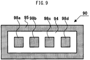
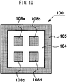
- FIGs. 9 , 10 , and 11 are bottom views of the LED devices 90, 100, and 110, respectively.
- Each of the LED devices 90, 100, and 110 has the circuit configuration illustrated in FIG. 7 like the LED device 60 of the third embodiment.
- the three LED dies 71, 72, and 73 see FIG. 7
- a phosphor layer, and a reflection layer are arranged on submount substrates 94, 104, and 114, respectively.
- a frame-shaped electrode 95 is arranged on the periphery of the bottom of the LED device 90, and inside electrodes 98a, 98b, 98c, and 98d are arranged inside the frame-shaped electrode 95.
- the frame-shaped electrode 95 is connected to the ground wire of the mother substrate, and the frame-shaped electrode 95 is not connected to the electrodes of the LED dies 71, 72, 73.
- One of the inside electrodes 98a, 98b, 98c, and 98d is connected to the common anode 75 (see FIG. 7 ) and the other inside electrodes are connected to the cathodes 78a, 78b, and 78c of the LEDs 71, 72, and 73, respectively.
- a frame-shaped electrode 105 is arranged on the periphery of the bottom of the LED device 100, and four inside electrodes 108a, 108b, 108c, and 108d are arranged inside the frame-shaped electrode 105 so that each is located at the vertex of a square.
- the frame-shaped electrode 105 is connected to the ground wire of the mother substrate, and the frame-shaped electrode 105 is not connected to the electrodes of the LED dies 71, 72, and 73.
- One of the inside electrodes 108a, 108b, 108c, and 108d is connected to the common anode 75 (see FIG. 7 ) and the other inside electrodes are connected to the cathodes 78a, 78b, and 78c of the LED dies 71, 72, and 73, respectively.
- a frame-shaped electrode 115 is arranged on the periphery of the bottom of the LED device 110, and an inside electrode 118a is arranged inside the frame-shaped electrode 115, and three inside electrodes 118b, 118c, and 118d are linearly arranged adjacent to the inside electrode 118a.
- the frame-shaped electrode 115 is connected to the ground wire of the mother substrate, and the frame-shaped electrode 115 is not connected to the electrodes of the LED dies 71, 72, and 73.
- the inside electrode 118a is connected to the common anode 75 (see FIG. 7 ) and the inside electrodes 118b, 118c, and 118d are connected to the cathodes 78a, 78b, and 78c of the LED dies 71, 72, and 73, respectively.
- the frame-shaped electrode is formed across the entire periphery of the bottom of the LED device.
- the perimeter of the bottom of the LED device may be sealed by solder along the periphery, by forming the frame-shaped electrode across the entire periphery of the bottom of the LED device. Since the perimeter of the bottom of the LED device is sealed by solder along the periphery, electrically conductive foreign matter, such as moisture, may be prevented from invading the bottom of the LED device without performing special coating processing.
- the inside electrode that is arranged inside the frame-shaped electrode is connected to the wire outside the frame-shaped electrode via the through hole that penetrates through the mother substrate in order to cross the frame-shaped electrode.
- an LED device 120 in which inside electrodes may be connected to the wire outside the frame-shaped electrode without using the through hole is explained as an eighth embodiment.
- FIG. 12A is a perspective view of the LED device 120 and FIG. 12B is a bottom view of the LED device 120.
- an LED die, a phosphor layer 128, and a reflection layer 127 are arranged on a submount substrate 121. Since the sectional structure of the LED device 120 is substantially the same as that of the LED device 1 of the first embodiment, the section view of the LED device 120 is not provided.
- a frame-shaped electrode 122 that is arranged on the bottom of the LED device 120 has three sides, i.e., an upper side, a left side that extends downward from the left end of the upper side, and a right side that extends downward from the right end of the upper side, and therefore the configuration of the frame-shaped electrode 122 is formed as the frame-shaped configuration from which one side is missing.
- the frame-shaped electrode 122 is formed into a U shape.
- the frame-shaped electrode 122 includes electroplating patterns 122a, 122b, and 122c.
- An inside electrode 123 is formed so as to be surrounded by the frame-shaped electrode 122.
- the inside electrode 123 includes an electroplating pattern 123a.
- the submount substrates 121 are connected to one another, and arranged on a large-sized substrate, and the submount substrates 121 on a large-sized substrate are individualized by cutting the large-sized substrate.
- the electroplating pattern 122a is connected to the electroplating pattern 122c
- the electroplating pattern 122b is connected to the electroplating pattern 123a.
- FIG. 13 is a plan view illustrating a solder pattern that is formed on the mother substrate on which the LED device 120 is mounted.
- the solder pattern that is illustrated in FIG. 13 has a solder pattern 124 that is connected to the frame-shaped electrode 122 (see FIGs. 12A and 12B ) and a solder pattern 125 that is connected to the inside electrode 123.
- a wire on the mother substrate that is connected to the inside electrode 123 is formed so as to be connected from the opening side of the solder pattern 124 to the solder pattern 125.
- the LED device 120 may simplify the wire of the mother substrate on which the LED device 120 is mounted. Foreign matter is prevented from invading the bottom of the LED device 120, by performing coating processing to apply a protective member only to the side on the opening side of the solder pattern 124 (see FIG. 13 ) after mounting the LED device 120 on the mother substrate.
- the entire periphery of the bottom of the conventional LED device should be coated in order to prevent foreign matter from invading the bottom of the LED device, whereas only one side of the bottom of the LED device 120 is coated.
- 3A to 3C is arranged across the entire periphery of the bottom of the LED device, it is not necessary to form a through hole for the wire of the inside electrode in the mother substrate by using the LED device 120. Since if the LED device 120 is used, the wire of the mother substrate is simplified, the planar size of the submount substrate 121 (see FIGs. 12A and 12B ) may be reduced, and the size of the LED device 120 may be reduced.
- a plurality of inside electrodes may be arranged in an LED device including a frame-shaped electrode in the shape of U. If a plurality of inside electrodes is arranged in an LED device including a frame-shaped electrode in the shape of U, the LED device may have a plurality of LED dies, and the colors of light emitted from the LED dies that are mounted in the LED device may be different from one another.
- the reflection layer 2 is arranged on the top thereof and the phosphor layer 3 is arranged on the side thereof.
- the structure of the element that is arranged on the surface of the submount substrate on which the LED die is arranged is not limited to that of the embodiments.
- the LED die may be flip-chip-mounted.
- the reflection layer that is arranged on the top of the LED device may be removed.
- the reflection member may be arranged on the side instead of the top.
- the frame-shaped electrodes 5, 65, and 85 are connected to the anode of the LED die and each of the inside electrodes 8, 68a to 68c, and 88a to 88c is connected to the cathode of the LED die.
- the inside electrode when the frame-shaped electrode is connected to the anode, the inside electrode is connected to the cathode and when the frame-shaped electrode is connected to the cathode, the inside electrode is connected to the anode.
- the frame-shaped electrode may be connected to one of the anode and the cathode, and some inside electrodes may be connected to the anode, and some others may be connected to the cathode.
- the frame-shaped electrode 55 and the inside electrode 58a may be connected to the anode of the LED die 9 (see FIG. 4 ), and the inside electrode 58b may be connected to the cathode of the LED die 9.
Landscapes
- Led Device Packages (AREA)
Abstract
Description
- The present invention relates to an LED device.
- An LED device is known, in which an LED in a bare chip state (hereinafter, also referred to as an LED die) is mounted onto a submount substrate and which is packaged by coating with a resin or the like. The submount substrate is a small-sized substrate that is inserted between the LED die and a large-sized substrate (hereinafter, also referred to as a mother substrate) on which other electronic parts, such as resistors capacitors, are mounted, and the submount substrate is also referred to as an interposer. The submount substrate includes an anode electrode and a cathode electrode on the bottom in opposition to the surface of the mother substrate (e.g., see Patent Document 1).
-
FIG. 14 is a perspective view of a conventional semiconductor package corresponding toFIG. 1 ofPatent Document 1, andFIG. 15 is a bottom view of a conventional semiconductor package corresponding toFIG. 4 ofPatent Document 1. - An LED device (semiconductor package) 20 has a submount substrate (wire substrate) 10 and an LED die (LED element) 61 flip-chip-mounted on the submount substrate. Bumps 61a and 61b joined to the cathode electrode and the anode electrode, respectively, of the LED die are provided on the bottom of the
LED die 61. Thesubmount substrate 10 has aceramic substrate 11 and a pair ofelectrodes ceramic substrate 11. Each of the pair ofelectrodes surface electrodes side electrodes 12b and 13b (not illustrated), andbottom electrodes LED device 20. TheLED die 61 is joined to land portions that are formed on thesurface electrodes electrodes bumps - Further, pairs of
recesses vias submount substrate 10. Theside electrodes 12b and 13b are arranged in the pair ofrecesses vias LED die 61 from the surface of the submount substrate to the bottom. - The
bottom electrodes LED device 20. The size and spacing of the upper-side electrodes LED die 61, whereas the size and spacing of thebottom electrodes - [Patent Document 1]
Japanese Laid Open Patent Document No. 2005-191097 FIGs. 1 and4 ) - The bottom of the conventional LED device (semiconductor package) 20 illustrated in
FIG. 14 may be stained, if a liquid is attached to the mother substrate on which the LED device is mounted when the LED device is mounted on the mother substrate. Foreign matter, such as a liquid, which is attached to the bottom of the LED device may cause migration and a short circuit between the electrodes of the LED device. - The object of present invention is to solve the above problem, i.e., to provide an LED device whose bottom is not stained, even if foreign matter, such as a liquid, is attached.
- The LED device of the present invention has an LED die, a submount substrate on the surface of which the LED die is mounted, a frame-shaped electrode arranged along the periphery of the bottom of the submount substrate, and an inside electrode surrounded by the frame-shaped electrode and connected to the electrode of the LED die.
- When the LED device is mounted on the mother substrate, the frame-shaped electrode and the inside electrode are connected to the wire electrode on the mother substrate by solder. Solder used to join the frame-shaped electrode to the mother substrate exists along the periphery of the bottom of the submount substrate that forms the bottom of the LED device, and therefore the sides along which the frame-shaped electrode is arranged on the bottom of the submount substrate are sealed. Thus, in the LED device mounted on the mother substrate, foreign matter, such as a liquid, no longer invades the bottom of the LED device through the sides along which the frame-shaped electrode is arranged.
- In the LED device of the present invention, the frame-shaped electrode may be arranged across the entire periphery of the bottom.
- In the LED device of the present invention, the shape of the bottom is rectangular and the frame-shaped electrode may be arranged along the three sides of the bottom.
- In the LED device of the present invention, the frame-shaped electrode may be connected to the electrode of the LED die.
- In the LED device of the present invention, the frame-shaped electrode may be connected to the ground wire that is formed on the mother substrate on which the LED device is mounted.
- The LED device of the present invention may have at least two inside electrodes.
- In the LED device of the present invention, the LED dies may be a red light-emitting LED die, a green light-emitting LED die, and a blue light-emitting LED die.
- The LED device of the present invention includes a frame-shaped electrode that is arranged along the periphery of the bottom, and therefore the bottom of the LED device may be prevented from being stained by sealing the sides along which the frame-shaped electrode is arranged on the bottom of the LED device that is mounted on the mother substrate.
-
-
FIG. 1 is a perspective view of an LED device of a first embodiment; -
FIG. 2 is a perspective view illustrating the state where the LED device illustrated inFIG. 1 is mounted on a mother substrate; -
FIG. 3A is an external view of the LED device illustrated inFIG. 1 ; -
FIG. 3B is an external view of the LED device illustrated inFIG. 1 ; -
FIG. 3C is an external view of the LED device illustrated inFIG. 1 ; -
FIG. 4 is a section view of the LED device illustrated inFIG. 1 ; -
FIG. 5A is a bottom view of the LED device of a second embodiment; -
FIG. 5B is a view illustrating a mounted state of the LED device illustrated inFIG. 5A ; -
FIG. 6A is a bottom view of the LED device of a third embodiment; -
FIG. 6B is a view illustrating a mounted state of the LED device illustrated inFIG. 6A ; -
FIG. 7 is a circuit diagram of the LED device illustrated inFIG. 6A ; -
FIG. 8A is a bottom view of the LED device of a forth embodiment; -
FIG. 8B is a section view illustrating a mounted state of the LED device illustrated inFIG. 8A ; -
FIG. 9 is a bottom view of the LED device of a fifth embodiment; -
FIG. 10 is a bottom view of a sixth embodiment; -
FIG. 11 is a bottom view of the LED device of a seventh embodiment; -
FIG. 12A is a perspective view of an eighth embodiment; -
FIG. 12B is a bottom view of the LED device illustrated inFIG. 12A ; -
FIG. 13 is a plan view illustrating a solder pattern that is formed on the mother substrate on which the LED device illustrated inFIG. 12A is mounted; -
FIG. 14 is a perspective view of a conventional LED device; and -
FIG. 15 is a bottom view of a conventional LED device illustrated inFIG. 14 . - Hereinafter, with reference to
FIGs. 1 to 13 of the attached drawings, preferred embodiments of the present invention are explained in detail. In the explanation of the drawings, identical symbols are used for the identical or corresponding element, and therefore duplicated explanation is omitted. Further, the scale of the members has been changed appropriately for explanation. -
FIG. 1 is a perspective view of anLED device 1 of a first embodiment. TheLED device 1 has areflection layer 2 that is arranged on the uppermost part, aphosphor layer 3 that is arranged beneath thereflection layer 2, asubmount substrate 4 that is arranged beneath thephosphor layer 3, and a frame-shapedelectrode 5 that is arranged beneath thesubmount substrate 4. -
FIG. 2 is a perspective view illustrating the state where theLED device 1 of the first embodiment is mounted on amother substrate 7. TheLED device 1 is connected to a wire electrode, not illustrated, which is formed on themother substrate 7, bysolder 6. Thesolder 6 forms a fillet and surrounds theLED device 1. -
FIGs. 3A to 3C are external views of theLED device 1 of the first embodiment andFIG. 3A is a plan view of theLED device 1,FIG. 3B is a front view of theLED device 1, andFIG. 3C is a bottom view of theLED device 1. Thereflection layer 2 is seen from the surface direction of theLED device 1. The frame-shapedelectrode 5, thesubmount substrate 4 on which the frame-shapedelectrode 5 is formed, and thephosphor layer 3 and thereflection layer 2 stacked on thesubmount substrate 4, respectively, are seen from the front direction of theLED device 1. The frame-shapedelectrode 5 that is formed and arranged so as to surround the periphery of the bottom of thesubmount substrate 4, and aninside electrode 8 that is surrounded by the frame-shapedelectrode 5 are seen from the bottom direction of theLED device 1. The bottom of thesubmount substrate 4 is seen between the frame-shapedelectrode 5 and theinside electrode 8. -
FIG. 4 is a section view along AA line inFIG. 2 .Surface electrodes submount substrate 4, and throughholes 4c and 4d that penetrate through from the surface to the bottom are formed in thesubmount substrate 4. Thesurface electrode 4a is connected to the frame-shapedelectrode 5 via the through hole 4c, and thesurface electrode 4b is connected to theinside electrode 8 via the throughhole 4d. An LED die 9 is die-bonded to the surface of thesurface electrode 4b. Awire 9a connects the electrode of the LED die 9 and thesurface electrodes wire 9a are coated by thephosphor layer 3. Thereflection layer 2 is arranged on thephosphor layer 3.Wire electrodes mother substrate 7. Thewire electrode 7a is connected to the frame-shapedelectrode 5 via thesolder 6 and thewire electrode 7b is connected to theinside electrode 8 via thesolder 6. - The material that forms the
submount substrate 4 is selected from among insulting materials whose thermal conductivity is high. In the present embodiment, alumina whose thermal conductivity is excellent and whose reflectance is high is used as the material that forms thesubmount substrate 4. When the reflection layer is arranged on the surface of thesubmount substrate 4, aluminum nitride whose reflectance is low and whose thermal conductivity is high may be used as the material that forms thesubmount substrate 4. Further, a resin or a metal substrate whose surface has been subjected to insulation processing may be used as the material of thesubmount substrate 4. - Each of the
surface electrodes electrode 5, and theinside electrode 8 is formed by stacking Ni and Au on Cu. The hollow part of the throughholes 4c and 4d is filled with an electrically conductive member, such as cupper paste. The LED die 9 is a blue light-emitting diode and includes a sapphire substrate and a semiconductor layer that is stacked on the sapphire. The thickness of the sapphire substrate is about 150 µm and the thickness of the semiconductor layer is slightly less than 10 µm. The semiconductor layer includes an n-type GaN layer and a p-type GaN layer that is stacked on the n-type GaN layer, and the boundary part between the n-type GaN layer and the p-type GaN layer functions as a light-emitting layer. Further, the n-type GaN layer is connected to the cathode of the LED die 9 and the p-type GaN layer is connected to the anode of the LED die 9. - The
phosphor layer 3 is formed by curing silicone kneaded with phosphor. Thereflection layer 2 is formed by curing silicone kneaded with alumina or titanium oxide. Thereflection layer 2 may be a metal plate or a reflecting tape. Light emitted from the LED die 9 is reflected from the surface of thesubmount substrate 4 and from thereflection layer 2, and is emitted from the side of theLED device 1 after propagating through thephosphor layer 3. Part of the light that is emitted from the LED die 9 is wavelength-converted by the phosphor included in thephosphor layer 3. - Since the perimeter of the bottom of the
LED device 1 is sealed with thesolder 6, foreign matter, such as a stained liquid, is not likely to invade the bottom. Since the chances are low that the bottom of theLED device 1 is stained by foreign matter, such as a stained liquid, chances are low that a short circuit occurs between the electrodes of theLED device 1, and chances are low that migration will occur between theinside electrode 8 and the frame-shapedelectrode 5. When the inventors of the invention of the application attached salt as a stained liquid to the mother substrate mounting theLED device 1, no short circuit occurred between the electrodes of theLED device 1. - In the
LED device 1 of the first embodiment illustrated inFIGs. 1 to 4 , the frame-shapedelectrode 5 is connected to one of the electrodes of the anode and the cathode of the LED die 9, and theinside electrode 8 is connected to the other electrode of the anode and the cathode. However, in an LED device of some kind of embodiments, although electrodes arranged on the bottom are connected to the anode and the cathode, its frame-shaped electrode may be connected to neither the anode nor the cathode. With reference toFIGs. 5A and 5B , anLED device 50 of a second embodiment, in which the frame-shaped electrode is connected to neither the anode nor the cathode, is explained as the second embodiment. -
FIG. 5A is a bottom view of theLED device 50 of the second embodiment andFIG. 5B is a section view along AA line inFIG. 5A . An LED die 59, aphosphor layer 53, and areflection layer 52 are arranged on asubmount substrate 54 in theLED device 50, as in theLED device 1 of the first embodiment. However, since theLED device 50 has the identical external view as that of theLED device 1, a perspective view illustrating the external view of theLED device 50 is not provided (regarding embodiments to be explained below, a perspective view illustrating the external view is not provided). - A frame-shaped
electrode 55 is arranged on the periphery of the bottom of theLED device 50, and twoinside electrodes electrode 55. The frame-shapedelectrode 55 is connected to aground wire 57a of amother substrate 57, and the frame-shapedelectrode 55 is not connected to the LED die 59 that is mounted on thesubmount substrate 54. Theinside electrode 58a is connected to the anode of theLED device 59 via a throughhole 54d, asurface electrode 54a, and a wire. Theinside electrode 58b is connected to the cathode of the LED die 59 via a throughhole 54c, asurface electrode 54b, and awire 59a. - When the
LED device 50 is mounted on themother substrate 57, since the voltage level of the frame-shapedelectrode 55 that is formed on the periphery of the bottom is the ground level, and the frame-shapedelectrode 55 is not connected to the LED die 59, static electricity may not affect theLED device 50. - In the
LED devices FIG. 4 )) is mounted on thesubmount substrates FIGs. 6A and6B andFIG. 7 , anLED device 60 in which three LED dies are mounted on asubmount substrate 64 is explained as a third embodiment. -
FIG. 6A is a bottom view of theLED device 60,FIG. 6B is a section view along AA line inFIG. 6A , andFIG. 7 is a circuit diagram of theLED device 60. In theLED device 60, LED dies 71, 72, and 73, aphosphor layer 63, and areflection layer 62 are arranged on thesubmount substrate 64. A frame-shapedelectrode 65 is arranged on the periphery of the bottom of theLED device 60, and threeinside electrodes electrode 65. The three insideelectrodes inside electrode 68a is located at the vertex and theinside electrodes electrode 65 is a common electrode that is connected to the anode of each of the LED dies 71, 72, and 73 and theinside electrodes cathodes - The LED dies 71, 72, and 73 are a red light-emitting diode, a green light-emitting diode, and a blue light-emitting diode, respectively. The LED dies 71, 72, and 73 share an
anode 75, and include thecathodes anode 75 of the LED dies 71, 72, and 73 is connected to the frame-shapedelectrode 65 via awire 69a, asurface electrode 64a, and a throughhole 64c. Thecathodes inside electrodes cathode 78b of the LED die 72 is connected to theinside electrode 68b via a wire, asurface electrode 642b, and a throughhole 642d. Thecathode 78c of the LED die 73 is connected to theinside electrode 68c via a wire, asurface electrode 643b, and a throughhole 643d. In theLED device 60, since the currents that flow through the LED dies 71, 72, and 73, respectively may be individually controlled, light may be emitted in a variety of colors by changing the currents that flow through the LED dies 71, 72, and 73. - In the
LED device 60 of the third embodiment, theinside electrodes FIGs. 8A and8B , anLED device 80 in which inside electrodes are linearly arranged is explained as a fourth embodiment.FIG. 8A is a bottom view of theLED device 80. TheLED device 80 has the circuit configuration illustrated inFIG. 7 like theLED device 60 of the third embodiment. In theLED device 80, the three LED dies 71, 72, and 73 (seeFIG. 7 ), aphosphor layer 83, and areflection layer 82 are arranged on asubmount substrate 84. A frame-shapedelectrode 85 is arranged on the periphery of the bottom of theLED device 80, and threeinside electrodes electrode 85. The frame-shapedelectrode 85 is a common electrode that is connected to the anodes of the LED dies 71, 72, and 73. Theanodes 75 of the LED dies 71, 72, and 73 are connected to the frame-shapedelectrode 85 via awire 89a, asurface electrode 84a, and a throughhole 84c. Theinside electrodes cathodes cathode 78a of the LED die 71 is connected to theinside electrode 88a via a wire, asurface electrode 841b, and a throughhole 841d. Thecathode 78b of the LED die 72 is connected to theinside electrode 88b via a wire, asurface electrode 842b, and a throughhole 842d. Thecathode 78c of the LED die 73 is connected to theinside electrode 88c via a wire, asurface electrode 843b, and a through hole 843d. - In the
LED devices electrodes FIGs. 9 ,10 , and11 ,LED devices -
FIGs. 9 ,10 , and11 are bottom views of theLED devices LED devices FIG. 7 like theLED device 60 of the third embodiment. In theLED devices FIG. 7 ), a phosphor layer, and a reflection layer are arranged onsubmount substrates - A frame-shaped
electrode 95 is arranged on the periphery of the bottom of theLED device 90, and insideelectrodes electrode 95. The frame-shapedelectrode 95 is connected to the ground wire of the mother substrate, and the frame-shapedelectrode 95 is not connected to the electrodes of the LED dies 71, 72, 73. One of theinside electrodes FIG. 7 ) and the other inside electrodes are connected to thecathodes LEDs - A frame-shaped
electrode 105 is arranged on the periphery of the bottom of theLED device 100, and fourinside electrodes electrode 105 so that each is located at the vertex of a square. The frame-shapedelectrode 105 is connected to the ground wire of the mother substrate, and the frame-shapedelectrode 105 is not connected to the electrodes of the LED dies 71, 72, and 73. One of theinside electrodes FIG. 7 ) and the other inside electrodes are connected to thecathodes - A frame-shaped
electrode 115 is arranged on the periphery of the bottom of theLED device 110, and aninside electrode 118a is arranged inside the frame-shapedelectrode 115, and three insideelectrodes inside electrode 118a. The frame-shapedelectrode 115 is connected to the ground wire of the mother substrate, and the frame-shapedelectrode 115 is not connected to the electrodes of the LED dies 71, 72, and 73. Theinside electrode 118a is connected to the common anode 75 (seeFIG. 7 ) and theinside electrodes cathodes - In the
LED devices FIGs. 12A ,12B, and 13 , anLED device 120 in which inside electrodes may be connected to the wire outside the frame-shaped electrode without using the through hole is explained as an eighth embodiment. -
FIG. 12A is a perspective view of theLED device 120 andFIG. 12B is a bottom view of theLED device 120. In theLED device 120, an LED die, aphosphor layer 128, and areflection layer 127 are arranged on asubmount substrate 121. Since the sectional structure of theLED device 120 is substantially the same as that of theLED device 1 of the first embodiment, the section view of theLED device 120 is not provided. A frame-shapedelectrode 122 that is arranged on the bottom of theLED device 120 has three sides, i.e., an upper side, a left side that extends downward from the left end of the upper side, and a right side that extends downward from the right end of the upper side, and therefore the configuration of the frame-shapedelectrode 122 is formed as the frame-shaped configuration from which one side is missing. In other words, the frame-shapedelectrode 122 is formed into a U shape. The frame-shapedelectrode 122 includeselectroplating patterns inside electrode 123 is formed so as to be surrounded by the frame-shapedelectrode 122. Theinside electrode 123 includes anelectroplating pattern 123a. When theLED device 120 is manufactured, thesubmount substrates 121 are connected to one another, and arranged on a large-sized substrate, and thesubmount substrates 121 on a large-sized substrate are individualized by cutting the large-sized substrate. When a plurality ofLED devices 120 is arranged on the large-sized substrate, theelectroplating pattern 122a is connected to theelectroplating pattern 122c, and theelectroplating pattern 122b is connected to theelectroplating pattern 123a. -
FIG. 13 is a plan view illustrating a solder pattern that is formed on the mother substrate on which theLED device 120 is mounted. The solder pattern that is illustrated inFIG. 13 has asolder pattern 124 that is connected to the frame-shaped electrode 122 (seeFIGs. 12A and12B ) and asolder pattern 125 that is connected to theinside electrode 123. A wire on the mother substrate that is connected to theinside electrode 123 is formed so as to be connected from the opening side of thesolder pattern 124 to thesolder pattern 125. - The
LED device 120 may simplify the wire of the mother substrate on which theLED device 120 is mounted. Foreign matter is prevented from invading the bottom of theLED device 120, by performing coating processing to apply a protective member only to the side on the opening side of the solder pattern 124 (seeFIG. 13 ) after mounting theLED device 120 on the mother substrate. The entire periphery of the bottom of the conventional LED device (seeFIGs. 14 and 15 ) should be coated in order to prevent foreign matter from invading the bottom of the LED device, whereas only one side of the bottom of theLED device 120 is coated. When theLED device 120 is compared with theLED device 1 of the first embodiment, in which the frame-shapedelectrode 5 or the like (seeFIGs. 3A to 3C ) is arranged across the entire periphery of the bottom of the LED device, it is not necessary to form a through hole for the wire of the inside electrode in the mother substrate by using theLED device 120. Since if theLED device 120 is used, the wire of the mother substrate is simplified, the planar size of the submount substrate 121 (seeFIGs. 12A and12B ) may be reduced, and the size of theLED device 120 may be reduced. - In the
LED device 120 of the eighth embodiment, although the one insideelectrode 123 is arranged, a plurality of inside electrodes may be arranged in an LED device including a frame-shaped electrode in the shape of U. If a plurality of inside electrodes is arranged in an LED device including a frame-shaped electrode in the shape of U, the LED device may have a plurality of LED dies, and the colors of light emitted from the LED dies that are mounted in the LED device may be different from one another. - In the
LED devices reflection layer 2 is arranged on the top thereof and thephosphor layer 3 is arranged on the side thereof. However, in the LED devices of the embodiments, the structure of the element that is arranged on the surface of the submount substrate on which the LED die is arranged is not limited to that of the embodiments. For example, in the LED devices of the embodiments, the LED die may be flip-chip-mounted. Further, in the LED devices of the embodiments, the reflection layer that is arranged on the top of the LED device may be removed. Furthermore, in the LED device of the embodiments, the reflection member may be arranged on the side instead of the top. - In the
LED devices electrodes inside electrodes FIGs. 5A and 5B , the frame-shapedelectrode 55 and theinside electrode 58a may be connected to the anode of the LED die 9 (seeFIG. 4 ), and theinside electrode 58b may be connected to the cathode of the LED die 9. -
- 1, 50, 60, 80, 90, 100, 110, 120 LED device;
- 2, 52, 62, 82, 127 reflection layer;
- 3, 53, 63, 83, 128 phosphor layer;
- 4, 54, 64, 84, 94, 104, 114, 121 submount substrate;
- 4a, 4b, 54a, 54b, 64a, 642b, 643b, 84a, 841b, 842b, 843b surface electrode;
- 4c, 4d, 54c, 54d, 64c, 642d, 643d, 84c, 841d, 842d, 843d through holes;
- 5, 55, 65, 85, 95, 105, 115, 122 frame-shaped electrode;
- 6, 6a, 56, 56a, 56b, 66, 662, 663, 86, 861, 862, 863 solder;
- 7, 57, 67, 87 mother substrate;
- 7a, 7b, 57a, 57b, 57c, 67a, 672b, 673b, 87a, 871b, 872b, 873b wire electrode;
- 8, 58a, 58b, 68a-c, 88a-c, 98a-d, 108a-d, 118a-d,123 inside electrode;
- 9, 59, 71, 72, 73 LED die;
- 9a, 59a, 69a, 89a wire;
- 75 anode;
- 78a, 78b, 78c cathode;
- 122a, 122b, 122C, 123a electroplating pattern; and
- 124, 125 solder pattern
Claims (7)
- An LED device comprising:an LED die;a submount substrate on the surface of which the LED die is mounted;a frame-shaped electrode that is arranged along the periphery of the bottom of the submount substrate; andan inside electrode that is surrounded by the frame-shaped electrode and which is connected to the electrode of the LED die.
- The LED device according to claim 1, wherein
the frame-shaped electrode is arranged across the entire periphery of the bottom. - The LED device according to claim 1, wherein
the shape of the bottom is rectangular, and
the frame-shaped electrode is arranged along three sides of the bottom. - The LED device according to any one of claims 1 to 3, wherein
the frame-shaped electrode is connected to the electrode of the LED die. - The LED device according to any one of claims 1 to 3, wherein
the frame-shaped electrode is connected to a ground wire that is formed on a mother substrate on which the LED device is mounted. - The LED device according to any one of claims 1 to 5, comprising at least the two inside electrodes.
- The LED device according to any one of claims 1 to 6, wherein
the LED dies are a red light-emitting LED die, a green light-emitting LED die, and a blue light-emitting LED die.
Applications Claiming Priority (3)
| Application Number | Priority Date | Filing Date | Title |
|---|---|---|---|
| JP2013136338 | 2013-06-28 | ||
| JP2013173114 | 2013-08-23 | ||
| PCT/JP2014/066540 WO2014208495A1 (en) | 2013-06-28 | 2014-06-23 | Led device |
Publications (3)
| Publication Number | Publication Date |
|---|---|
| EP3016154A1 true EP3016154A1 (en) | 2016-05-04 |
| EP3016154A4 EP3016154A4 (en) | 2016-12-14 |
| EP3016154B1 EP3016154B1 (en) | 2020-08-05 |
Family
ID=52141830
Family Applications (1)
| Application Number | Title | Priority Date | Filing Date |
|---|---|---|---|
| EP14817164.8A Active EP3016154B1 (en) | 2013-06-28 | 2014-06-23 | Led device |
Country Status (5)
| Country | Link |
|---|---|
| US (1) | US10170674B2 (en) |
| EP (1) | EP3016154B1 (en) |
| JP (1) | JP5693800B1 (en) |
| CN (1) | CN105359284B (en) |
| WO (1) | WO2014208495A1 (en) |
Families Citing this family (10)
| Publication number | Priority date | Publication date | Assignee | Title |
|---|---|---|---|---|
| US10170674B2 (en) * | 2013-06-28 | 2019-01-01 | Citizen Watch Co., Ltd. | LED device |
| TWI575785B (en) * | 2014-10-30 | 2017-03-21 | 新世紀光電股份有限公司 | Illuminating device |
| KR101730977B1 (en) * | 2016-01-14 | 2017-04-28 | 피에스아이 주식회사 | Nano-scale LED electrode assembly |
| WO2019235565A1 (en) * | 2018-06-08 | 2019-12-12 | 日機装株式会社 | Semiconductor light emitting device |
| TWI684835B (en) * | 2018-12-25 | 2020-02-11 | 同泰電子科技股份有限公司 | Substrate structure with high reflectivity and manufacturing method thereof |
| JP6852822B2 (en) * | 2019-05-30 | 2021-03-31 | 日亜化学工業株式会社 | Light emitting module and its manufacturing method |
| US11681090B2 (en) * | 2019-05-30 | 2023-06-20 | Nichia Corporation | Light emitting module and method of manufacturing same |
| JP7497578B2 (en) | 2020-02-26 | 2024-06-11 | 富士フイルムビジネスイノベーション株式会社 | Light emitting device, optical device and information processing device |
| JP2021136306A (en) * | 2020-02-26 | 2021-09-13 | 富士フイルムビジネスイノベーション株式会社 | Light emitting device, optical device and information processing device |
| US11899307B2 (en) * | 2020-09-25 | 2024-02-13 | Boe Optical Science And Technology Co., Ltd. | Flexible printed circuit, light bar, backlight module and liquid crystal display device |
Family Cites Families (28)
| Publication number | Priority date | Publication date | Assignee | Title |
|---|---|---|---|---|
| JPS6352422A (en) * | 1986-08-22 | 1988-03-05 | Hitachi Tobu Semiconductor Ltd | Electronic device and its chip and its substrate |
| JP2005191097A (en) | 2003-12-24 | 2005-07-14 | Kawaguchiko Seimitsu Co Ltd | Semiconductor package |
| US9070850B2 (en) * | 2007-10-31 | 2015-06-30 | Cree, Inc. | Light emitting diode package and method for fabricating same |
| US20070080360A1 (en) * | 2005-10-06 | 2007-04-12 | Url Mirsky | Microelectronic interconnect substrate and packaging techniques |
| JP5212532B2 (en) * | 2005-10-31 | 2013-06-19 | 豊田合成株式会社 | Method for manufacturing light emitting device |
| JP4940883B2 (en) | 2005-10-31 | 2012-05-30 | 豊田合成株式会社 | Light emitting device |
| US7928462B2 (en) * | 2006-02-16 | 2011-04-19 | Lg Electronics Inc. | Light emitting device having vertical structure, package thereof and method for manufacturing the same |
| CN101304059B (en) * | 2007-05-09 | 2010-09-08 | 富士迈半导体精密工业(上海)有限公司 | Light-emitting diode assembly and light-emitting diode display device |
| US8436371B2 (en) * | 2007-05-24 | 2013-05-07 | Cree, Inc. | Microscale optoelectronic device packages |
| US9172012B2 (en) * | 2007-10-31 | 2015-10-27 | Cree, Inc. | Multi-chip light emitter packages and related methods |
| JP5558665B2 (en) * | 2007-11-27 | 2014-07-23 | パナソニック株式会社 | Light emitting device |
| JP5345363B2 (en) * | 2008-06-24 | 2013-11-20 | シャープ株式会社 | Light emitting device |
| WO2011083923A2 (en) * | 2010-01-07 | 2011-07-14 | Seoul Opto Device Co., Ltd. | Light emitting diode having electrode pads |
| CN103222073B (en) * | 2010-08-03 | 2017-03-29 | 财团法人工业技术研究院 | Light-emitting diode chip, light-emitting diode package structure, and method for forming the above |
| EP2418700B1 (en) * | 2010-08-09 | 2017-11-01 | LG Innotek Co., Ltd. | Light emitting device |
| DE102010034924A1 (en) | 2010-08-20 | 2012-02-23 | Osram Opto Semiconductors Gmbh | Optoelectronic semiconductor component |
| KR20120082190A (en) * | 2011-01-13 | 2012-07-23 | 삼성엘이디 주식회사 | Light emitting device package |
| US9240524B2 (en) * | 2012-03-05 | 2016-01-19 | Seoul Viosys Co., Ltd. | Light-emitting device and method of manufacturing the same |
| JP5989388B2 (en) * | 2012-04-19 | 2016-09-07 | 新光電気工業株式会社 | Package and package manufacturing method |
| US20130328074A1 (en) * | 2012-06-11 | 2013-12-12 | Cree, Inc. | Led package with multiple element light source and encapsulant having planar surfaces |
| CN104718620B (en) * | 2012-10-24 | 2018-01-02 | 夏普株式会社 | Light-emitting device |
| CN202996902U (en) | 2012-11-21 | 2013-06-12 | 深圳市斯迈得光电子有限公司 | Safe and reliable LED lamp bead |
| KR20140094752A (en) * | 2013-01-22 | 2014-07-31 | 삼성전자주식회사 | An electronic device package and a packaging substrate for the same |
| DE102013104840A1 (en) * | 2013-05-10 | 2014-11-13 | Osram Opto Semiconductors Gmbh | Radiation-emitting semiconductor component and method for producing radiation-emitting semiconductor components |
| US10170674B2 (en) * | 2013-06-28 | 2019-01-01 | Citizen Watch Co., Ltd. | LED device |
| GB201400264D0 (en) | 2014-01-08 | 2014-02-26 | Element Six Ltd | Synthetic diamond optical mirrors |
| KR20160023011A (en) * | 2014-08-20 | 2016-03-03 | 삼성전자주식회사 | Light emitting device package |
| EP2988341B1 (en) * | 2014-08-22 | 2017-04-05 | LG Innotek Co., Ltd. | Light emitting device package |
-
2014
- 2014-06-23 US US14/901,471 patent/US10170674B2/en active Active
- 2014-06-23 JP JP2014544288A patent/JP5693800B1/en active Active
- 2014-06-23 WO PCT/JP2014/066540 patent/WO2014208495A1/en not_active Ceased
- 2014-06-23 CN CN201480037154.6A patent/CN105359284B/en active Active
- 2014-06-23 EP EP14817164.8A patent/EP3016154B1/en active Active
Also Published As
| Publication number | Publication date |
|---|---|
| US10170674B2 (en) | 2019-01-01 |
| CN105359284A (en) | 2016-02-24 |
| CN105359284B (en) | 2019-05-14 |
| EP3016154B1 (en) | 2020-08-05 |
| WO2014208495A1 (en) | 2014-12-31 |
| JP5693800B1 (en) | 2015-04-01 |
| JPWO2014208495A1 (en) | 2017-02-23 |
| EP3016154A4 (en) | 2016-12-14 |
| US20160197253A1 (en) | 2016-07-07 |
Similar Documents
| Publication | Publication Date | Title |
|---|---|---|
| EP3016154B1 (en) | Led device | |
| US9035333B2 (en) | Semiconductor light emitting device | |
| JP6581766B2 (en) | Light emitting diode module and manufacturing method thereof | |
| CN105990499A (en) | Light emitting diode package structure and manufacturing method thereof | |
| US9966332B2 (en) | Solid-state device including a conductive bump connected to a metal pattern and method of manufacturing the same | |
| US10263159B2 (en) | Light-emitter mounting package, light-emitting device, and light-emitting module | |
| CN107534268A (en) | Package for mounting optical element, electronic device, and electronic module | |
| KR20150026732A (en) | Semiconductor light emitting device | |
| KR20190129178A (en) | Light emitting element package with thin film pad and manufacturing method thereof | |
| US20260101619A1 (en) | Led package structure | |
| US10879438B2 (en) | Light emitting module and manufacturing method of light emitting module | |
| JP2022033187A (en) | Semiconductor light emitting device | |
| CN103794695A (en) | Flip chip type light-emitting diode (LED) chip | |
| US10515882B2 (en) | Semiconductor device package including electrode solder pads and additional solder pads | |
| US11532776B2 (en) | Semiconductor light-emitting device | |
| JP2019153766A (en) | Light emitting device and manufacturing method thereof | |
| JP2019117818A (en) | Mounting substrate, light emitting device, and manufacturing method of light emitting device | |
| US20220069184A1 (en) | Semiconductor light emitting device and method for manufacturing the same | |
| CN211045429U (en) | Flexible multilayer construction and LESD packaging | |
| KR20140110257A (en) | Light emitting device package | |
| KR101341771B1 (en) | Led package | |
| KR100791736B1 (en) | Electronic component, its manufacturing method, light emitting diode package and its manufacturing method | |
| TW201533928A (en) | Light emitting diode package and method for forming the same | |
| KR101034142B1 (en) | Light emitting device and manufacturing method | |
| JP2019087549A (en) | LED package and method of manufacturing the same |
Legal Events
| Date | Code | Title | Description |
|---|---|---|---|
| PUAI | Public reference made under article 153(3) epc to a published international application that has entered the european phase |
Free format text: ORIGINAL CODE: 0009012 |
|
| 17P | Request for examination filed |
Effective date: 20151222 |
|
| AK | Designated contracting states |
Kind code of ref document: A1 Designated state(s): AL AT BE BG CH CY CZ DE DK EE ES FI FR GB GR HR HU IE IS IT LI LT LU LV MC MK MT NL NO PL PT RO RS SE SI SK SM TR |
|
| AX | Request for extension of the european patent |
Extension state: BA ME |
|
| DAX | Request for extension of the european patent (deleted) | ||
| A4 | Supplementary search report drawn up and despatched |
Effective date: 20161114 |
|
| RIC1 | Information provided on ipc code assigned before grant |
Ipc: H01L 33/62 20100101AFI20161108BHEP |
|
| RAP1 | Party data changed (applicant data changed or rights of an application transferred) |
Owner name: CITIZEN WATCH CO., LTD. Owner name: CITIZEN ELECTRONICS CO., LTD. |
|
| STAA | Information on the status of an ep patent application or granted ep patent |
Free format text: STATUS: EXAMINATION IS IN PROGRESS |
|
| 17Q | First examination report despatched |
Effective date: 20190520 |
|
| GRAP | Despatch of communication of intention to grant a patent |
Free format text: ORIGINAL CODE: EPIDOSNIGR1 |
|
| STAA | Information on the status of an ep patent application or granted ep patent |
Free format text: STATUS: GRANT OF PATENT IS INTENDED |
|
| INTG | Intention to grant announced |
Effective date: 20200221 |
|
| GRAS | Grant fee paid |
Free format text: ORIGINAL CODE: EPIDOSNIGR3 |
|
| GRAA | (expected) grant |
Free format text: ORIGINAL CODE: 0009210 |
|
| STAA | Information on the status of an ep patent application or granted ep patent |
Free format text: STATUS: THE PATENT HAS BEEN GRANTED |
|
| AK | Designated contracting states |
Kind code of ref document: B1 Designated state(s): AL AT BE BG CH CY CZ DE DK EE ES FI FR GB GR HR HU IE IS IT LI LT LU LV MC MK MT NL NO PL PT RO RS SE SI SK SM TR |
|
| REG | Reference to a national code |
Ref country code: GB Ref legal event code: FG4D |
|
| REG | Reference to a national code |
Ref country code: CH Ref legal event code: EP |
|
| REG | Reference to a national code |
Ref country code: AT Ref legal event code: REF Ref document number: 1299961 Country of ref document: AT Kind code of ref document: T Effective date: 20200815 |
|
| REG | Reference to a national code |
Ref country code: DE Ref legal event code: R096 Ref document number: 602014068682 Country of ref document: DE |
|
| REG | Reference to a national code |
Ref country code: IE Ref legal event code: FG4D |
|
| REG | Reference to a national code |
Ref country code: LT Ref legal event code: MG4D |
|
| REG | Reference to a national code |
Ref country code: NL Ref legal event code: MP Effective date: 20200805 |
|
| REG | Reference to a national code |
Ref country code: AT Ref legal event code: MK05 Ref document number: 1299961 Country of ref document: AT Kind code of ref document: T Effective date: 20200805 |
|
| PG25 | Lapsed in a contracting state [announced via postgrant information from national office to epo] |
Ref country code: HR Free format text: LAPSE BECAUSE OF FAILURE TO SUBMIT A TRANSLATION OF THE DESCRIPTION OR TO PAY THE FEE WITHIN THE PRESCRIBED TIME-LIMIT Effective date: 20200805 Ref country code: LT Free format text: LAPSE BECAUSE OF FAILURE TO SUBMIT A TRANSLATION OF THE DESCRIPTION OR TO PAY THE FEE WITHIN THE PRESCRIBED TIME-LIMIT Effective date: 20200805 Ref country code: AT Free format text: LAPSE BECAUSE OF FAILURE TO SUBMIT A TRANSLATION OF THE DESCRIPTION OR TO PAY THE FEE WITHIN THE PRESCRIBED TIME-LIMIT Effective date: 20200805 Ref country code: SE Free format text: LAPSE BECAUSE OF FAILURE TO SUBMIT A TRANSLATION OF THE DESCRIPTION OR TO PAY THE FEE WITHIN THE PRESCRIBED TIME-LIMIT Effective date: 20200805 Ref country code: BG Free format text: LAPSE BECAUSE OF FAILURE TO SUBMIT A TRANSLATION OF THE DESCRIPTION OR TO PAY THE FEE WITHIN THE PRESCRIBED TIME-LIMIT Effective date: 20201105 Ref country code: PT Free format text: LAPSE BECAUSE OF FAILURE TO SUBMIT A TRANSLATION OF THE DESCRIPTION OR TO PAY THE FEE WITHIN THE PRESCRIBED TIME-LIMIT Effective date: 20201207 Ref country code: ES Free format text: LAPSE BECAUSE OF FAILURE TO SUBMIT A TRANSLATION OF THE DESCRIPTION OR TO PAY THE FEE WITHIN THE PRESCRIBED TIME-LIMIT Effective date: 20200805 Ref country code: NO Free format text: LAPSE BECAUSE OF FAILURE TO SUBMIT A TRANSLATION OF THE DESCRIPTION OR TO PAY THE FEE WITHIN THE PRESCRIBED TIME-LIMIT Effective date: 20201105 Ref country code: FI Free format text: LAPSE BECAUSE OF FAILURE TO SUBMIT A TRANSLATION OF THE DESCRIPTION OR TO PAY THE FEE WITHIN THE PRESCRIBED TIME-LIMIT Effective date: 20200805 Ref country code: GR Free format text: LAPSE BECAUSE OF FAILURE TO SUBMIT A TRANSLATION OF THE DESCRIPTION OR TO PAY THE FEE WITHIN THE PRESCRIBED TIME-LIMIT Effective date: 20201106 |
|
| PG25 | Lapsed in a contracting state [announced via postgrant information from national office to epo] |
Ref country code: NL Free format text: LAPSE BECAUSE OF FAILURE TO SUBMIT A TRANSLATION OF THE DESCRIPTION OR TO PAY THE FEE WITHIN THE PRESCRIBED TIME-LIMIT Effective date: 20200805 Ref country code: RS Free format text: LAPSE BECAUSE OF FAILURE TO SUBMIT A TRANSLATION OF THE DESCRIPTION OR TO PAY THE FEE WITHIN THE PRESCRIBED TIME-LIMIT Effective date: 20200805 Ref country code: LV Free format text: LAPSE BECAUSE OF FAILURE TO SUBMIT A TRANSLATION OF THE DESCRIPTION OR TO PAY THE FEE WITHIN THE PRESCRIBED TIME-LIMIT Effective date: 20200805 Ref country code: PL Free format text: LAPSE BECAUSE OF FAILURE TO SUBMIT A TRANSLATION OF THE DESCRIPTION OR TO PAY THE FEE WITHIN THE PRESCRIBED TIME-LIMIT Effective date: 20200805 Ref country code: IS Free format text: LAPSE BECAUSE OF FAILURE TO SUBMIT A TRANSLATION OF THE DESCRIPTION OR TO PAY THE FEE WITHIN THE PRESCRIBED TIME-LIMIT Effective date: 20201205 |
|
| PG25 | Lapsed in a contracting state [announced via postgrant information from national office to epo] |
Ref country code: CZ Free format text: LAPSE BECAUSE OF FAILURE TO SUBMIT A TRANSLATION OF THE DESCRIPTION OR TO PAY THE FEE WITHIN THE PRESCRIBED TIME-LIMIT Effective date: 20200805 Ref country code: DK Free format text: LAPSE BECAUSE OF FAILURE TO SUBMIT A TRANSLATION OF THE DESCRIPTION OR TO PAY THE FEE WITHIN THE PRESCRIBED TIME-LIMIT Effective date: 20200805 Ref country code: EE Free format text: LAPSE BECAUSE OF FAILURE TO SUBMIT A TRANSLATION OF THE DESCRIPTION OR TO PAY THE FEE WITHIN THE PRESCRIBED TIME-LIMIT Effective date: 20200805 Ref country code: SM Free format text: LAPSE BECAUSE OF FAILURE TO SUBMIT A TRANSLATION OF THE DESCRIPTION OR TO PAY THE FEE WITHIN THE PRESCRIBED TIME-LIMIT Effective date: 20200805 Ref country code: RO Free format text: LAPSE BECAUSE OF FAILURE TO SUBMIT A TRANSLATION OF THE DESCRIPTION OR TO PAY THE FEE WITHIN THE PRESCRIBED TIME-LIMIT Effective date: 20200805 |
|
| REG | Reference to a national code |
Ref country code: DE Ref legal event code: R097 Ref document number: 602014068682 Country of ref document: DE |
|
| PG25 | Lapsed in a contracting state [announced via postgrant information from national office to epo] |
Ref country code: AL Free format text: LAPSE BECAUSE OF FAILURE TO SUBMIT A TRANSLATION OF THE DESCRIPTION OR TO PAY THE FEE WITHIN THE PRESCRIBED TIME-LIMIT Effective date: 20200805 |
|
| PLBE | No opposition filed within time limit |
Free format text: ORIGINAL CODE: 0009261 |
|
| STAA | Information on the status of an ep patent application or granted ep patent |
Free format text: STATUS: NO OPPOSITION FILED WITHIN TIME LIMIT |
|
| PG25 | Lapsed in a contracting state [announced via postgrant information from national office to epo] |
Ref country code: SK Free format text: LAPSE BECAUSE OF FAILURE TO SUBMIT A TRANSLATION OF THE DESCRIPTION OR TO PAY THE FEE WITHIN THE PRESCRIBED TIME-LIMIT Effective date: 20200805 |
|
| 26N | No opposition filed |
Effective date: 20210507 |
|
| PG25 | Lapsed in a contracting state [announced via postgrant information from national office to epo] |
Ref country code: IT Free format text: LAPSE BECAUSE OF FAILURE TO SUBMIT A TRANSLATION OF THE DESCRIPTION OR TO PAY THE FEE WITHIN THE PRESCRIBED TIME-LIMIT Effective date: 20200805 |
|
| PG25 | Lapsed in a contracting state [announced via postgrant information from national office to epo] |
Ref country code: SI Free format text: LAPSE BECAUSE OF FAILURE TO SUBMIT A TRANSLATION OF THE DESCRIPTION OR TO PAY THE FEE WITHIN THE PRESCRIBED TIME-LIMIT Effective date: 20200805 |
|
| PG25 | Lapsed in a contracting state [announced via postgrant information from national office to epo] |
Ref country code: MC Free format text: LAPSE BECAUSE OF FAILURE TO SUBMIT A TRANSLATION OF THE DESCRIPTION OR TO PAY THE FEE WITHIN THE PRESCRIBED TIME-LIMIT Effective date: 20200805 |
|
| REG | Reference to a national code |
Ref country code: CH Ref legal event code: PL |
|
| GBPC | Gb: european patent ceased through non-payment of renewal fee |
Effective date: 20210623 |
|
| REG | Reference to a national code |
Ref country code: BE Ref legal event code: MM Effective date: 20210630 |
|
| PG25 | Lapsed in a contracting state [announced via postgrant information from national office to epo] |
Ref country code: LU Free format text: LAPSE BECAUSE OF NON-PAYMENT OF DUE FEES Effective date: 20210623 |
|
| PG25 | Lapsed in a contracting state [announced via postgrant information from national office to epo] |
Ref country code: LI Free format text: LAPSE BECAUSE OF NON-PAYMENT OF DUE FEES Effective date: 20210630 Ref country code: IE Free format text: LAPSE BECAUSE OF NON-PAYMENT OF DUE FEES Effective date: 20210623 Ref country code: GB Free format text: LAPSE BECAUSE OF NON-PAYMENT OF DUE FEES Effective date: 20210623 Ref country code: CH Free format text: LAPSE BECAUSE OF NON-PAYMENT OF DUE FEES Effective date: 20210630 |
|
| PG25 | Lapsed in a contracting state [announced via postgrant information from national office to epo] |
Ref country code: FR Free format text: LAPSE BECAUSE OF NON-PAYMENT OF DUE FEES Effective date: 20210630 |
|
| PG25 | Lapsed in a contracting state [announced via postgrant information from national office to epo] |
Ref country code: BE Free format text: LAPSE BECAUSE OF NON-PAYMENT OF DUE FEES Effective date: 20210630 |
|
| PG25 | Lapsed in a contracting state [announced via postgrant information from national office to epo] |
Ref country code: HU Free format text: LAPSE BECAUSE OF FAILURE TO SUBMIT A TRANSLATION OF THE DESCRIPTION OR TO PAY THE FEE WITHIN THE PRESCRIBED TIME-LIMIT; INVALID AB INITIO Effective date: 20140623 |
|
| PG25 | Lapsed in a contracting state [announced via postgrant information from national office to epo] |
Ref country code: CY Free format text: LAPSE BECAUSE OF FAILURE TO SUBMIT A TRANSLATION OF THE DESCRIPTION OR TO PAY THE FEE WITHIN THE PRESCRIBED TIME-LIMIT Effective date: 20200805 |
|
| PG25 | Lapsed in a contracting state [announced via postgrant information from national office to epo] |
Ref country code: MK Free format text: LAPSE BECAUSE OF FAILURE TO SUBMIT A TRANSLATION OF THE DESCRIPTION OR TO PAY THE FEE WITHIN THE PRESCRIBED TIME-LIMIT Effective date: 20200805 |
|
| PG25 | Lapsed in a contracting state [announced via postgrant information from national office to epo] |
Ref country code: TR Free format text: LAPSE BECAUSE OF FAILURE TO SUBMIT A TRANSLATION OF THE DESCRIPTION OR TO PAY THE FEE WITHIN THE PRESCRIBED TIME-LIMIT Effective date: 20200805 |
|
| PG25 | Lapsed in a contracting state [announced via postgrant information from national office to epo] |
Ref country code: MT Free format text: LAPSE BECAUSE OF FAILURE TO SUBMIT A TRANSLATION OF THE DESCRIPTION OR TO PAY THE FEE WITHIN THE PRESCRIBED TIME-LIMIT Effective date: 20200805 |
|
| REG | Reference to a national code |
Ref country code: DE Ref legal event code: R079 Ref document number: 602014068682 Country of ref document: DE Free format text: PREVIOUS MAIN CLASS: H01L0033620000 Ipc: H10H0020857000 |
|
| PGFP | Annual fee paid to national office [announced via postgrant information from national office to epo] |
Ref country code: DE Payment date: 20250429 Year of fee payment: 12 |