EP3013598B1 - Verfahren zur herstellung eines mehrschichtkörpers sowie mehrschichtkörper - Google Patents
Verfahren zur herstellung eines mehrschichtkörpers sowie mehrschichtkörper Download PDFInfo
- Publication number
- EP3013598B1 EP3013598B1 EP14733628.3A EP14733628A EP3013598B1 EP 3013598 B1 EP3013598 B1 EP 3013598B1 EP 14733628 A EP14733628 A EP 14733628A EP 3013598 B1 EP3013598 B1 EP 3013598B1
- Authority
- EP
- European Patent Office
- Prior art keywords
- layer
- decorative
- resist
- zones
- metal layer
- Prior art date
- Legal status (The legal status is an assumption and is not a legal conclusion. Google has not performed a legal analysis and makes no representation as to the accuracy of the status listed.)
- Active
Links
- 238000004519 manufacturing process Methods 0.000 title claims description 40
- 239000010410 layer Substances 0.000 claims description 923
- 229910052751 metal Inorganic materials 0.000 claims description 176
- 239000002184 metal Substances 0.000 claims description 176
- 238000000034 method Methods 0.000 claims description 80
- 230000010076 replication Effects 0.000 claims description 67
- 239000004922 lacquer Substances 0.000 claims description 48
- 230000003287 optical effect Effects 0.000 claims description 28
- 230000005670 electromagnetic radiation Effects 0.000 claims description 25
- 238000005530 etching Methods 0.000 claims description 25
- 239000002904 solvent Substances 0.000 claims description 21
- 239000000049 pigment Substances 0.000 claims description 17
- 230000005540 biological transmission Effects 0.000 claims description 16
- 230000005855 radiation Effects 0.000 claims description 14
- 238000007639 printing Methods 0.000 claims description 12
- 238000004040 coloring Methods 0.000 claims description 9
- 239000012790 adhesive layer Substances 0.000 claims description 8
- 239000003086 colorant Substances 0.000 claims description 7
- 239000002356 single layer Substances 0.000 claims description 7
- 230000002186 photoactivation Effects 0.000 claims description 6
- 230000000007 visual effect Effects 0.000 claims description 6
- 239000000654 additive Substances 0.000 claims description 2
- 230000000996 additive effect Effects 0.000 claims description 2
- 238000002329 infrared spectrum Methods 0.000 claims description 2
- 238000001228 spectrum Methods 0.000 claims description 2
- 238000002211 ultraviolet spectrum Methods 0.000 claims description 2
- 238000001429 visible spectrum Methods 0.000 claims description 2
- 239000003795 chemical substances by application Substances 0.000 claims 5
- 239000004150 EU approved colour Substances 0.000 claims 2
- 229940006093 opthalmologic coloring agent diagnostic Drugs 0.000 claims 2
- 239000010408 film Substances 0.000 description 37
- 238000002834 transmittance Methods 0.000 description 28
- HEMHJVSKTPXQMS-UHFFFAOYSA-M sodium hydroxide Inorganic materials [OH-].[Na+] HEMHJVSKTPXQMS-UHFFFAOYSA-M 0.000 description 23
- 239000002346 layers by function Substances 0.000 description 20
- 239000000463 material Substances 0.000 description 20
- 230000008569 process Effects 0.000 description 19
- 229920002120 photoresistant polymer Polymers 0.000 description 17
- 239000013067 intermediate product Substances 0.000 description 11
- CDBYLPFSWZWCQE-UHFFFAOYSA-L Sodium Carbonate Chemical compound [Na+].[Na+].[O-]C([O-])=O CDBYLPFSWZWCQE-UHFFFAOYSA-L 0.000 description 10
- 239000000975 dye Substances 0.000 description 10
- 239000011888 foil Substances 0.000 description 10
- 239000006096 absorbing agent Substances 0.000 description 8
- 239000000543 intermediate Substances 0.000 description 7
- 229920003023 plastic Polymers 0.000 description 7
- 229910052782 aluminium Inorganic materials 0.000 description 6
- XAGFODPZIPBFFR-UHFFFAOYSA-N aluminium Chemical compound [Al] XAGFODPZIPBFFR-UHFFFAOYSA-N 0.000 description 6
- 239000004033 plastic Substances 0.000 description 6
- 239000000758 substrate Substances 0.000 description 6
- 239000002966 varnish Substances 0.000 description 6
- 239000002253 acid Substances 0.000 description 5
- 230000004913 activation Effects 0.000 description 5
- 230000015572 biosynthetic process Effects 0.000 description 5
- 239000002105 nanoparticle Substances 0.000 description 5
- 239000003973 paint Substances 0.000 description 5
- 239000004800 polyvinyl chloride Substances 0.000 description 5
- 229920000915 polyvinyl chloride Polymers 0.000 description 5
- 229910000029 sodium carbonate Inorganic materials 0.000 description 5
- 239000000126 substance Substances 0.000 description 5
- RYGMFSIKBFXOCR-UHFFFAOYSA-N Copper Chemical compound [Cu] RYGMFSIKBFXOCR-UHFFFAOYSA-N 0.000 description 4
- BQCADISMDOOEFD-UHFFFAOYSA-N Silver Chemical compound [Ag] BQCADISMDOOEFD-UHFFFAOYSA-N 0.000 description 4
- 239000003513 alkali Substances 0.000 description 4
- 229910052802 copper Inorganic materials 0.000 description 4
- 239000010949 copper Substances 0.000 description 4
- 239000011521 glass Substances 0.000 description 4
- -1 polyethylene terephthalate Polymers 0.000 description 4
- 229920000139 polyethylene terephthalate Polymers 0.000 description 4
- 239000005020 polyethylene terephthalate Substances 0.000 description 4
- 230000001681 protective effect Effects 0.000 description 4
- 229910052709 silver Inorganic materials 0.000 description 4
- 239000004332 silver Substances 0.000 description 4
- 238000005507 spraying Methods 0.000 description 4
- 239000012876 carrier material Substances 0.000 description 3
- 238000000576 coating method Methods 0.000 description 3
- 238000007796 conventional method Methods 0.000 description 3
- 230000000694 effects Effects 0.000 description 3
- 239000012044 organic layer Substances 0.000 description 3
- 238000000059 patterning Methods 0.000 description 3
- 239000002985 plastic film Substances 0.000 description 3
- 239000000047 product Substances 0.000 description 3
- 239000011241 protective layer Substances 0.000 description 3
- 230000003362 replicative effect Effects 0.000 description 3
- 230000000717 retained effect Effects 0.000 description 3
- 239000004698 Polyethylene Substances 0.000 description 2
- 239000004743 Polypropylene Substances 0.000 description 2
- XECAHXYUAAWDEL-UHFFFAOYSA-N acrylonitrile butadiene styrene Chemical compound C=CC=C.C=CC#N.C=CC1=CC=CC=C1 XECAHXYUAAWDEL-UHFFFAOYSA-N 0.000 description 2
- 239000004676 acrylonitrile butadiene styrene Substances 0.000 description 2
- 229920000122 acrylonitrile butadiene styrene Polymers 0.000 description 2
- 230000008901 benefit Effects 0.000 description 2
- 229920006378 biaxially oriented polypropylene Polymers 0.000 description 2
- 239000011127 biaxially oriented polypropylene Substances 0.000 description 2
- 238000005266 casting Methods 0.000 description 2
- 239000000470 constituent Substances 0.000 description 2
- 238000005034 decoration Methods 0.000 description 2
- 230000007423 decrease Effects 0.000 description 2
- 238000010030 laminating Methods 0.000 description 2
- 239000007788 liquid Substances 0.000 description 2
- 238000007645 offset printing Methods 0.000 description 2
- 238000004806 packaging method and process Methods 0.000 description 2
- 239000000123 paper Substances 0.000 description 2
- 229920006255 plastic film Polymers 0.000 description 2
- 229920003229 poly(methyl methacrylate) Polymers 0.000 description 2
- 229920000058 polyacrylate Polymers 0.000 description 2
- 229920000642 polymer Polymers 0.000 description 2
- 239000004926 polymethyl methacrylate Substances 0.000 description 2
- 230000002787 reinforcement Effects 0.000 description 2
- 238000007650 screen-printing Methods 0.000 description 2
- 238000007789 sealing Methods 0.000 description 2
- 239000011734 sodium Substances 0.000 description 2
- 239000004753 textile Substances 0.000 description 2
- 229920001169 thermoplastic Polymers 0.000 description 2
- 239000004416 thermosoftening plastic Substances 0.000 description 2
- 238000007740 vapor deposition Methods 0.000 description 2
- VYZAMTAEIAYCRO-UHFFFAOYSA-N Chromium Chemical compound [Cr] VYZAMTAEIAYCRO-UHFFFAOYSA-N 0.000 description 1
- 239000004831 Hot glue Substances 0.000 description 1
- 239000004372 Polyvinyl alcohol Substances 0.000 description 1
- 229910010413 TiO 2 Inorganic materials 0.000 description 1
- 238000005299 abrasion Methods 0.000 description 1
- 230000009471 action Effects 0.000 description 1
- 230000003213 activating effect Effects 0.000 description 1
- 239000013543 active substance Substances 0.000 description 1
- 239000000853 adhesive Substances 0.000 description 1
- 230000001070 adhesive effect Effects 0.000 description 1
- 125000001931 aliphatic group Chemical group 0.000 description 1
- 239000000956 alloy Substances 0.000 description 1
- 229910045601 alloy Inorganic materials 0.000 description 1
- 238000000149 argon plasma sintering Methods 0.000 description 1
- 125000003354 benzotriazolyl group Chemical class N1N=NC2=C1C=CC=C2* 0.000 description 1
- 238000004061 bleaching Methods 0.000 description 1
- 239000011111 cardboard Substances 0.000 description 1
- 239000003518 caustics Substances 0.000 description 1
- 239000001913 cellulose Substances 0.000 description 1
- 229920002678 cellulose Polymers 0.000 description 1
- 230000008859 change Effects 0.000 description 1
- 239000011248 coating agent Substances 0.000 description 1
- 239000002131 composite material Substances 0.000 description 1
- 239000006071 cream Substances 0.000 description 1
- 238000000354 decomposition reaction Methods 0.000 description 1
- 230000001419 dependent effect Effects 0.000 description 1
- 238000009792 diffusion process Methods 0.000 description 1
- 230000009977 dual effect Effects 0.000 description 1
- 230000007613 environmental effect Effects 0.000 description 1
- 230000005284 excitation Effects 0.000 description 1
- 239000002657 fibrous material Substances 0.000 description 1
- 239000007850 fluorescent dye Substances 0.000 description 1
- PCHJSUWPFVWCPO-UHFFFAOYSA-N gold Chemical compound [Au] PCHJSUWPFVWCPO-UHFFFAOYSA-N 0.000 description 1
- 229910052737 gold Inorganic materials 0.000 description 1
- 239000010931 gold Substances 0.000 description 1
- 238000007646 gravure printing Methods 0.000 description 1
- 238000007641 inkjet printing Methods 0.000 description 1
- 229910052809 inorganic oxide Inorganic materials 0.000 description 1
- 238000000608 laser ablation Methods 0.000 description 1
- 239000004973 liquid crystal related substance Substances 0.000 description 1
- 239000000155 melt Substances 0.000 description 1
- 238000002844 melting Methods 0.000 description 1
- QSHDDOUJBYECFT-UHFFFAOYSA-N mercury Chemical compound [Hg] QSHDDOUJBYECFT-UHFFFAOYSA-N 0.000 description 1
- 229910052753 mercury Inorganic materials 0.000 description 1
- 238000001465 metallisation Methods 0.000 description 1
- 150000002739 metals Chemical class 0.000 description 1
- 238000010422 painting Methods 0.000 description 1
- 239000011087 paperboard Substances 0.000 description 1
- 238000006552 photochemical reaction Methods 0.000 description 1
- 229920000728 polyester Polymers 0.000 description 1
- 229920000573 polyethylene Polymers 0.000 description 1
- 229920001155 polypropylene Polymers 0.000 description 1
- 229920001296 polysiloxane Polymers 0.000 description 1
- 229920002689 polyvinyl acetate Polymers 0.000 description 1
- 239000011118 polyvinyl acetate Substances 0.000 description 1
- 229920002451 polyvinyl alcohol Polymers 0.000 description 1
- 239000011253 protective coating Substances 0.000 description 1
- 239000002994 raw material Substances 0.000 description 1
- 239000004065 semiconductor Substances 0.000 description 1
- 238000004544 sputter deposition Methods 0.000 description 1
- 230000037072 sun protection Effects 0.000 description 1
- 230000000475 sunscreen effect Effects 0.000 description 1
- 239000000516 sunscreening agent Substances 0.000 description 1
- 230000003746 surface roughness Effects 0.000 description 1
- 238000010345 tape casting Methods 0.000 description 1
- 229920001187 thermosetting polymer Polymers 0.000 description 1
- 239000010409 thin film Substances 0.000 description 1
- 238000009281 ultraviolet germicidal irradiation Methods 0.000 description 1
Images


Classifications
-
- B—PERFORMING OPERATIONS; TRANSPORTING
- B42—BOOKBINDING; ALBUMS; FILES; SPECIAL PRINTED MATTER
- B42D—BOOKS; BOOK COVERS; LOOSE LEAVES; PRINTED MATTER CHARACTERISED BY IDENTIFICATION OR SECURITY FEATURES; PRINTED MATTER OF SPECIAL FORMAT OR STYLE NOT OTHERWISE PROVIDED FOR; DEVICES FOR USE THEREWITH AND NOT OTHERWISE PROVIDED FOR; MOVABLE-STRIP WRITING OR READING APPARATUS
- B42D25/00—Information-bearing cards or sheet-like structures characterised by identification or security features; Manufacture thereof
- B42D25/30—Identification or security features, e.g. for preventing forgery
-
- B—PERFORMING OPERATIONS; TRANSPORTING
- B42—BOOKBINDING; ALBUMS; FILES; SPECIAL PRINTED MATTER
- B42D—BOOKS; BOOK COVERS; LOOSE LEAVES; PRINTED MATTER CHARACTERISED BY IDENTIFICATION OR SECURITY FEATURES; PRINTED MATTER OF SPECIAL FORMAT OR STYLE NOT OTHERWISE PROVIDED FOR; DEVICES FOR USE THEREWITH AND NOT OTHERWISE PROVIDED FOR; MOVABLE-STRIP WRITING OR READING APPARATUS
- B42D25/00—Information-bearing cards or sheet-like structures characterised by identification or security features; Manufacture thereof
- B42D25/40—Manufacture
- B42D25/405—Marking
- B42D25/415—Marking using chemicals
- B42D25/42—Marking using chemicals by photographic processes
-
- B—PERFORMING OPERATIONS; TRANSPORTING
- B05—SPRAYING OR ATOMISING IN GENERAL; APPLYING FLUENT MATERIALS TO SURFACES, IN GENERAL
- B05D—PROCESSES FOR APPLYING FLUENT MATERIALS TO SURFACES, IN GENERAL
- B05D7/00—Processes, other than flocking, specially adapted for applying liquids or other fluent materials to particular surfaces or for applying particular liquids or other fluent materials
- B05D7/50—Multilayers
-
- B—PERFORMING OPERATIONS; TRANSPORTING
- B42—BOOKBINDING; ALBUMS; FILES; SPECIAL PRINTED MATTER
- B42D—BOOKS; BOOK COVERS; LOOSE LEAVES; PRINTED MATTER CHARACTERISED BY IDENTIFICATION OR SECURITY FEATURES; PRINTED MATTER OF SPECIAL FORMAT OR STYLE NOT OTHERWISE PROVIDED FOR; DEVICES FOR USE THEREWITH AND NOT OTHERWISE PROVIDED FOR; MOVABLE-STRIP WRITING OR READING APPARATUS
- B42D25/00—Information-bearing cards or sheet-like structures characterised by identification or security features; Manufacture thereof
- B42D25/30—Identification or security features, e.g. for preventing forgery
- B42D25/324—Reliefs
-
- B—PERFORMING OPERATIONS; TRANSPORTING
- B42—BOOKBINDING; ALBUMS; FILES; SPECIAL PRINTED MATTER
- B42D—BOOKS; BOOK COVERS; LOOSE LEAVES; PRINTED MATTER CHARACTERISED BY IDENTIFICATION OR SECURITY FEATURES; PRINTED MATTER OF SPECIAL FORMAT OR STYLE NOT OTHERWISE PROVIDED FOR; DEVICES FOR USE THEREWITH AND NOT OTHERWISE PROVIDED FOR; MOVABLE-STRIP WRITING OR READING APPARATUS
- B42D25/00—Information-bearing cards or sheet-like structures characterised by identification or security features; Manufacture thereof
- B42D25/30—Identification or security features, e.g. for preventing forgery
- B42D25/328—Diffraction gratings; Holograms
-
- B—PERFORMING OPERATIONS; TRANSPORTING
- B42—BOOKBINDING; ALBUMS; FILES; SPECIAL PRINTED MATTER
- B42D—BOOKS; BOOK COVERS; LOOSE LEAVES; PRINTED MATTER CHARACTERISED BY IDENTIFICATION OR SECURITY FEATURES; PRINTED MATTER OF SPECIAL FORMAT OR STYLE NOT OTHERWISE PROVIDED FOR; DEVICES FOR USE THEREWITH AND NOT OTHERWISE PROVIDED FOR; MOVABLE-STRIP WRITING OR READING APPARATUS
- B42D25/00—Information-bearing cards or sheet-like structures characterised by identification or security features; Manufacture thereof
- B42D25/30—Identification or security features, e.g. for preventing forgery
- B42D25/351—Translucent or partly translucent parts, e.g. windows
-
- B—PERFORMING OPERATIONS; TRANSPORTING
- B42—BOOKBINDING; ALBUMS; FILES; SPECIAL PRINTED MATTER
- B42D—BOOKS; BOOK COVERS; LOOSE LEAVES; PRINTED MATTER CHARACTERISED BY IDENTIFICATION OR SECURITY FEATURES; PRINTED MATTER OF SPECIAL FORMAT OR STYLE NOT OTHERWISE PROVIDED FOR; DEVICES FOR USE THEREWITH AND NOT OTHERWISE PROVIDED FOR; MOVABLE-STRIP WRITING OR READING APPARATUS
- B42D25/00—Information-bearing cards or sheet-like structures characterised by identification or security features; Manufacture thereof
- B42D25/30—Identification or security features, e.g. for preventing forgery
- B42D25/36—Identification or security features, e.g. for preventing forgery comprising special materials
- B42D25/373—Metallic materials
-
- B—PERFORMING OPERATIONS; TRANSPORTING
- B42—BOOKBINDING; ALBUMS; FILES; SPECIAL PRINTED MATTER
- B42D—BOOKS; BOOK COVERS; LOOSE LEAVES; PRINTED MATTER CHARACTERISED BY IDENTIFICATION OR SECURITY FEATURES; PRINTED MATTER OF SPECIAL FORMAT OR STYLE NOT OTHERWISE PROVIDED FOR; DEVICES FOR USE THEREWITH AND NOT OTHERWISE PROVIDED FOR; MOVABLE-STRIP WRITING OR READING APPARATUS
- B42D25/00—Information-bearing cards or sheet-like structures characterised by identification or security features; Manufacture thereof
- B42D25/30—Identification or security features, e.g. for preventing forgery
- B42D25/36—Identification or security features, e.g. for preventing forgery comprising special materials
- B42D25/378—Special inks
- B42D25/387—Special inks absorbing or reflecting ultraviolet light
-
- B—PERFORMING OPERATIONS; TRANSPORTING
- B42—BOOKBINDING; ALBUMS; FILES; SPECIAL PRINTED MATTER
- B42D—BOOKS; BOOK COVERS; LOOSE LEAVES; PRINTED MATTER CHARACTERISED BY IDENTIFICATION OR SECURITY FEATURES; PRINTED MATTER OF SPECIAL FORMAT OR STYLE NOT OTHERWISE PROVIDED FOR; DEVICES FOR USE THEREWITH AND NOT OTHERWISE PROVIDED FOR; MOVABLE-STRIP WRITING OR READING APPARATUS
- B42D25/00—Information-bearing cards or sheet-like structures characterised by identification or security features; Manufacture thereof
- B42D25/40—Manufacture
- B42D25/405—Marking
- B42D25/41—Marking using electromagnetic radiation
-
- B—PERFORMING OPERATIONS; TRANSPORTING
- B42—BOOKBINDING; ALBUMS; FILES; SPECIAL PRINTED MATTER
- B42D—BOOKS; BOOK COVERS; LOOSE LEAVES; PRINTED MATTER CHARACTERISED BY IDENTIFICATION OR SECURITY FEATURES; PRINTED MATTER OF SPECIAL FORMAT OR STYLE NOT OTHERWISE PROVIDED FOR; DEVICES FOR USE THEREWITH AND NOT OTHERWISE PROVIDED FOR; MOVABLE-STRIP WRITING OR READING APPARATUS
- B42D25/00—Information-bearing cards or sheet-like structures characterised by identification or security features; Manufacture thereof
- B42D25/40—Manufacture
- B42D25/405—Marking
- B42D25/43—Marking by removal of material
- B42D25/445—Marking by removal of material using chemical means, e.g. etching
-
- B—PERFORMING OPERATIONS; TRANSPORTING
- B42—BOOKBINDING; ALBUMS; FILES; SPECIAL PRINTED MATTER
- B42D—BOOKS; BOOK COVERS; LOOSE LEAVES; PRINTED MATTER CHARACTERISED BY IDENTIFICATION OR SECURITY FEATURES; PRINTED MATTER OF SPECIAL FORMAT OR STYLE NOT OTHERWISE PROVIDED FOR; DEVICES FOR USE THEREWITH AND NOT OTHERWISE PROVIDED FOR; MOVABLE-STRIP WRITING OR READING APPARATUS
- B42D25/00—Information-bearing cards or sheet-like structures characterised by identification or security features; Manufacture thereof
- B42D25/40—Manufacture
- B42D25/45—Associating two or more layers
Definitions
- the invention relates to a method for producing a multi-layer body with a carrier layer and a single-layer or multi-layer decorative layer formed on and / or in the carrier layer, as well as a multilayer body, a security element and a security document.
- optical security elements are often used to make it difficult to copy documents or products to prevent their misuse, especially counterfeiting.
- optical security elements find use for securing documents, banknotes, credit and debit cards, ID cards, packaging of high-quality products and the like.
- optically variable elements it is known to use optically variable elements as optical security elements which can not be duplicated by conventional copying methods.
- security elements with a structured metal layer, which is in the form of a text, logos or other pattern.
- a structured metal layer from a metal layer applied in a planar manner requires a large number of processes, in particular when producing particularly fine structures should be, which have a high security against counterfeiting.
- Object of the present invention is to provide a particularly difficult to reproduce multilayer body and a method for producing such a multilayer body.
- steps a) to e) of the process according to the invention are preferably carried out in the order indicated.
- the object is further achieved by a multi-layer body having a single-layer or multi-layered first decorative layer, a single or multi-layered second decorative layer and at least one metal layer arranged between the first and second decorative layers, wherein the metal layer is structured in such a way that the at least one metal layer is provided in a first region of the multilayer body in one or more first zones of the multilayer body in a first layer thickness and is provided in one or more second zones of the multilayer body in a second layer thickness different from the first layer thickness, wherein in particular the second layer thickness is equal to zero, and wherein the first and second decorative layer are congruent to each other and structured to the metal layer.
- the first and the second decorative layer and the metal layer preferably have partial structures, so that the first and second decorative layers in the first region in the first or second zones are at least partially congruent to one another and to the metal layer.
- Such a multilayer body is preferably obtainable by the methods described above.
- the multilayer body according to the invention can be used, for example, as a label, laminating film, hot stamping film or transfer film to provide an optical security element which is suitable for securing documents, banknotes, credit and debit cards, identity cards, packaging of high quality Products and the like is used.
- the decorative layers and the at least one register layer arranged precisely arranged metal layer can serve as an optical security element.
- the metal layer serves as a mask during the manufacture of the multilayer body, preferably as an exposure mask for exposure, i. the photoactivation of a photoactivatable layer, which may be comprised by the first and / or second decorative layer, or as a mask for protecting the first zones or the second zones, for example, prior to solvent attack, and on the finished multilayer body to provide an optical effect.
- the metal layer thus fulfills several completely different functions.
- step c) and / or step e) can in this case also take place only in a partial area of the multi-layer body, which then in particular forms the first area.
- the first and second decorative layers are patterned using the metal layer as a mask in the first region such that the first and second decorative layers are at least partially removed respectively in the first or second zones, or the metal layer using the first or second decorative layer as Mask is structured.
- register-accurate structuring of the first decorative layer, the second decorative layer and the metal layer relative to one another is achieved without additional use of registration devices and enables a very precise positionally accurate structuring of these layers relative to one another.
- the mask either as a separate unit, for example as a separate foil or as a separate glass plate / glass roller, or as a If there is a subsequently printed-on layer, there may be the problem that linear and / or non-linear distortions in the multilayer body caused by prior alignment of the mask on the multilayer body are not completely compensated for over the entire surface of the multilayer body due to thermal and / or mechanical straining process steps can, although the mask alignment on existing (usually arranged on the horizontal and / or vertical edges of the multilayer body) registration or registration marks is done. The tolerance fluctuates over the entire surface of the multilayer body in a relatively large area.
- the method preferably uses the first and second zones defined by the patterning of the first or second decorative layer or the metal layer, directly or indirectly, as a mask for structuring the remaining layers, so that these problems are avoided.
- the mask designed as a decorative layer or metal layer is therefore subjected to all subsequent process steps of the multilayer body, and thereby automatically follows all distortions possibly caused by these process steps in the multilayer body itself.
- no additional tolerances, in particular no additional tolerance fluctuations, over the surface of the multilayer body occur because the subsequent generation of a mask and the necessary register-accurate subsequent positioning of this independent of the previous process history mask is avoided.
- the tolerances or register accuracies in the method according to the invention are due only to possibly not absolutely exactly formed edges of the first and second zones and of the metal layer whose quality is determined by the particular manufacturing method used.
- the tolerances or register accuracies in the method according to the invention are approximately in the micrometer range, and thus far below the resolution of the eye; ie the unarmed human eye can no longer perceive existing tolerances.
- Register or register accuracy is to be understood as meaning the positional arrangement of superimposed layers.
- a layer comprises at least one layer.
- a decorative layer comprises one or more decorative and / or protective layers which are in particular formed as lacquer layers.
- the decorative layers can be arranged over the entire surface or in pattern-like structured form on the carrier layer.
- the object is arranged such that the object and the first and / or the second zone are perpendicular to the plane of the carrier layer overlap seen.
- the at least one metal layer may consist of a single metal layer or of a sequence of two or more metal layers, preferably different metal layers.
- the metal used for the metal layers is preferably aluminum, copper, gold, silver or an alloy of these metals.
- step c) i. for structuring the metal layer, a first resist layer which can be activated by means of electromagnetic radiation is applied to the side of the metal layer remote from the first decorative layer, and the first resist layer is exposed using an exposure mask by means of said electromagnetic radiation. Subsequently, further steps for structuring the metal layer, such as development, etching and stripping, then preferably follow.
- the second decorative layer applied in step d) comprises one or more second colored resist layers which can be activated by means of electromagnetic radiation.
- step e) the one or more second, colored resist layers are produced from the side of the carrier layer by means of said electromagnetic radiation exposed, wherein the metal layer serves as an exposure mask. In this way, the second decorative layer can be structured in the perfect register to the metal layer.
- the one or more second, colored resist layers comprise at least two different colorants or colorants of different concentration containing resist layers.
- One or more of the one or more second, colored resist layers may be applied in pattern form by means of a printing process. These colored resist layers are preferably formed in pattern form to form a first motif.
- the first resist layer is exposed in step c) from the side of the carrier layer, wherein the mask for exposing the first resist layer is formed by the first decorative layer.
- the first decorative layer has a first transmittance perpendicular to the plane of the carrier layer in the first region in the one or more first zones and a second transmittance greater in the one or more second zones compared to the first transmittance, said transmittances being preferably refer to an electromagnetic radiation having a suitable wavelength for photoactivation of the first resist layer.
- the first decorative layer thus acts as an exposure mask, since in the first zone it has a transmittance which is higher than the transmittance of the first second zone is lowered.
- the exposure takes place through the metal layer and thus the layer to be structured.
- the etching resist layer allows the metal layer to be patterned independently of the exposure of the first resist layer in this subregion, as a result of which further graphic effects can be achieved.
- the etching resist layer preferably consists of polyvinyl chloride.
- the first decorative layer also fulfills several completely different functions, namely the function of an exposure mask and the provision of optical information.
- the first decorative layer is preferably designed so that a viewer of an article decorated by means of the multi-layer body can view the at least one metal layer through the first decorative layer.
- the first decorative layer can be transparent or translucent.
- the first decorative layer forms a (colored) second, visible to the human observer motif, which is designed independently of the first and second zones.
- the first decorative layer can be colored for example transparent or translucent.
- the first resist layer is patterned in register with the first and second zones of the multilayer body, ie the structures of the structured first resist layer are arranged in register with the first and second zones of the decorative layer.
- the at least one metal layer is patterned in register with the resist layer.
- the use of the first decorative layer as the exposure mask for the first resist layer or the metal layer as the exposure mask for a second resist layer which may be covered by the second decorative layer inevitably results in perfect register accuracy of the respective exposure mask to the metal layer or the second decorative layer, i. the first decorative layer and the structured metal layer itself act at least in some areas as exposure masks.
- the first decorative layer or the metal layer and the exposure mask thus each form a common functional unit.
- the method which is as simple as it is effective, gives rise to a considerable advantage over conventional methods in which a separate exposure mask has to be registered in layers of the multilayer body, wherein in practice register deviations can only be completely avoided in very few cases.
- the first decorative layer prefferably comprises a first lacquer layer which is arranged in the first zone with a first layer thickness and in the second zone either not or with a smaller second layer thickness compared to the first layer thickness on the carrier layer, so that the first decorative layer in the first zone having said first transmittance and in the second zone said second transmittance.
- the mask function of the first decorative layer is realized in a simple manner.
- the paint layers can be particularly patterned by a printing process, such as gravure, offset printing, screen printing, inkjet printing, so that both the mask function and the desired optical effect can be realized.
- a printing process such as gravure, offset printing, screen printing, inkjet printing
- the paint layers contain a UV absorber and / or a colorant.
- the thickness and the material of the first decorative layer are chosen so that electromagnetic radiation with the appropriate wavelength for the photoactivation partially penetrates the first decorative layer in the first zone.
- the exposure mask formed by the first decorative layer is therefore designed to be radiation-permeable in the first zone.
- the thickness and the material of the first decorative layer are chosen such that the ratio between the second and the first transmittance is equal to or greater than 2.
- the ratio between the first and the second transmittance is preferably 1: 2, also referred to as contrast 1: 2.
- a contrast of 1: 2 is at least an order of magnitude lower than with conventional masks. It has hitherto not been customary to use a mask for exposing a resist layer, which mask has as little contrast as the preferably used first decorative layer described here. When exposing a resist to a conventional mask (eg, a chrome mask), there are opaque (OD> 2) and fully transparent areas; So the mask has a high contrast.
- a conventional mask eg, a chrome mask
- the area of the photoactivatable first resist layer (lower transmittance) exposed through the first zones is preferably activated to a lesser extent than the area of the photoactivatable first resist layer exposed through the second zones (greater transmittance).
- the first resist layer may be temporarily applied to the metal layer during the production of the multilayer body, where it serves to structure the metal layer, or else be part of the second decorative layer or serve for structuring the second decorative layer.
- the thickness and the material of the first decorative layer is selected so that the electromagnetic radiation, measured after passing through a layer package consisting of the carrier layer and the decorative layer, in the first zone a transmittance of about 0% to 30%, preferably from about 1% to 15% and in the second zone has a transmittance of about 60% to 100%, preferably from about 70% to 90%.
- the transmittances from these ranges of values are preferably selected such that a contrast of 1: 2 results.
- the first resist layer is exposed in step c) from the side facing away from the carrier layer, wherein for exposing the first resist layer, a mask between the first resist layer and a light source, which is used for exposure, is arranged.
- the mask has, viewed perpendicularly to the plane of the carrier layer, a first transmittance in the first region in the one or more first zones and a second transmittance in the one or more second zones in comparison to the first transmittance, wherein the transmittances are preferably on relate an electromagnetic radiation having a suitable wavelength for photoactivation of the first resist layer.
- an external mask can be used without register problems.
- the structures in the metal layer produced by means of the external mask then later act in the described manner as a mask for the generation of additional register-accurate structures in the first and / or second decorative layer.
- Exposure is the selective irradiation of a photoactivatable layer through an exposure mask with the aim of locally modifying the solubility of the photoactivatable layer by a photochemical reaction.
- photoactivatable layers which can be formed as photoresists:
- a first type of photoactivatable layers eg negative resist
- their solubility decreases by exposure compared to unexposed zones of the layer
- unexposed zones of the layer For example, because the light leads to the curing of the layer
- a second type of photoactivatable layers e.g., positive resist
- their solubility increases by exposure to unexposed areas of the layer, for example, because the light results in the decomposition of the layer.
- the resist layer can therefore be patterned, ie the resist layer is removed in the second zone, but remains in the first zone.
- the first resist layer is then preferably used as an etching mask for an etching step, by means of which the regions of the metal layer not covered with the first resist layer or one of the metal layers are removed. Subsequently, the first resist layer may be stripped, i. be removed.
- UV radiation is used for the exposure of the first and / or second resist layer, preferably with a radiation maximum in the region of 365 nm.
- the transmission properties of the decorative layer used as a mask can thus be different in the ultraviolet range than in the visual range.
- the structure of the mask is not dependent on the visually perceptible optical effect to be achieved by the decorative layers.
- PET polyethylene terephthalate
- PET polyethylene terephthalate
- first and / or second resist layer prefferably have a thickness in the range from 0.3 ⁇ m to 0.7 ⁇ m.
- step c) is carried out after step d), and in step c) the metal layer is structured using the second decorative layer as a mask, in particular by applying an etchant and removing the areas of the metal layer which are not protected by the mask.
- step e) then the first decorative layer using the Metal layer as a mask, in particular by applying a solvent and removing the not protected by the mask areas of the first decorative layer, structured.
- the second decorative layer has here in addition to the optical function achieved by the coloring so an additional function as a mask, on the basis of which subsequently the register-accurate structuring of the metal layer.
- an additional function as a mask
- the metal layer can in turn be used as a mask for structuring the first decorative layer, for example by removing the zones of the first decorative layer not covered by the metal layer by a solvent.
- the second decorative layer is applied by pattern printing, wherein the second decorative layer is provided in the first zones with a third layer thickness and is provided in the second zones with a fourth layer thickness different from the third layer thickness, in particular the fourth Layer thickness is zero.
- the second decorative layer is resistant to an etchant used for patterning the metal layer and to a solvent used for structuring the first decorative layer.
- the second decorative layer can serve both as a protective mask for structuring the metal layer and for structuring the first decorative layer.
- the second decorative layer comprises one or more colored layers, which are applied in particular by a printing process.
- the first resist layer and / or areas of the first decorative layer not protected by the metal layer are removed by a solvent.
- a preferred embodiment also provides for substantially completely removing ("stripping") the resist layer during the work step for structuring the metal layer or in a separate, subsequent, subsequent work step.
- step c the zones of the metal layer not protected by the first resist layer and / or the second decorative layer are removed by an etchant.
- an etchant such as an acid or alkali.
- the partial removal of the resist layer in the respective region and the regions of the metal layer which are thereby exposed take place in the same process step.
- a solvent / etchant such as a lye or acid which is capable of both the resist layer - in the case of a positive resist in the exposed region, in the case of a negative resist in the unexposed region - and the layer to be structured to remove, that attacks both materials.
- the resist layer must be formed so that they to remove the solvent or etchant to be structured when using a positive resist in the unexposed area, when using a negative resist in the exposed area at least for a sufficient time, that is resistant to the contact time of the solvent or etchant.
- the carrier layer comprises at least one functional layer, in particular a release layer and / or a protective lacquer layer, on the side facing the first decorative layer.
- the functional layer enables a problem-free detachment of the carrier layer from a transfer layer which comprises at least one layer of the first and second decorative layer and the metal layer
- first and / or second decorative layer comprise a replicate varnish layer into which a surface relief is molded, and / or that a surface relief is molded into the surface of the carrier layer facing the first decorative layer.
- the surface relief comprising a diffractive structure preferably having a spatial frequency between 200 and 2000 lines / mm, in particular a hologram, Kinegram ®, a linear grating or a cross grating, a diffractive structure zero order, in particular with a spatial frequency of more than 2000 lines / mm, a blazed grating, a refractive structure, in particular a microlens field or a retroreflective structure, an optical lens, a free-form surface structure, and / or a matt structure, in particular an isotropic or anisotropic matt structure.
- Matt structure refers to a structure with light-scattering properties, which preferably has a stochastic surface matt profile.
- Matt structures preferably have a relief depth (peak-to-valley, PV) between 100 nm and 5000 nm, more preferably between 200 nm and 2000 nm. Matt structures preferably have a surface roughness (Ra) between 50 nm and 2000 nm, more preferably between 100 nm and 1000 nm.
- the matte effect can either isotropic, ie equal to all azimuth angles, or anisotropic, ie varying at different azimuth angles.
- a replication layer is generally understood as meaning a layer which can be produced superficially with a relief structure. These include, for example, organic layers such as plastic or lacquer layers or inorganic layers such as inorganic plastics (for example silicones), semiconductor layers, metal layers etc., but also combinations thereof. It is preferred that the replication layer is formed as a replicate varnish layer.
- a radiation-curable or thermosetting replication layer or a thermoplastic replication lacquer layer can be applied, a relief can be molded into the replication layer, and the replication layer optionally cured with the embossment embossed therein.
- a compensating layer is applied which rests, in particular, on the surface regions of the first decorative layer, the second decorative layer and / or the carrier layer facing away from the carrier layer.
- the metal layer and the first resist layer are removed in the first or the second zone and present in the other region, or in the corresponding process variants in the zones protected by the second resist layer and in remaining area is removed.
- the compensating layer recessed areas / depressions of the metal layer, the first decorative layer and / or the second decorative layer can be at least partially filled. It is possible that by applying the compensating layer, recessed regions / depressions of the first or second resist layer are at least partially filled.
- the leveling layer may comprise one or more different layer materials.
- the compensation layer may be formed as a protective and / or adhesive and / or decorative layer.
- an adhesion-promoting layer (adhesive layer) to be applied to the side of the compensating layer facing away from the carrier layer, which layer may also have a multilayer structure.
- the target substrate can be, for example, paper, paperboard, textile or another fibrous material, or a plastic or a composite of, for example, paper, cardboard, textile and plastic, while being flexible or predominantly rigid.
- a protective coating is applied to the multilayer body on the side of the multilayer body facing away from the carrier layer. This protects the multilayer body from environmental influences and mechanical manipulations.
- first and / or second decorative layer is bleached by exposure.
- any remaining photoreactive substances in the unexposed areas of the multilayer body are reacted and prevents later uncontrolled bleaching. In this way, a particularly color-stable multilayer body is obtained.
- the multi-layer body comprises a particular full-surface carrier layer.
- carrier material based on PVC and PVC copolymer carrier material based on PVC and PVC copolymer
- Support material based on polyvinyl alcohol and polyvinyl acetate
- polyester support based on aliphatic raw materials.
- the carrier layer has a single-layer or multi-layer carrier film.
- a thickness of the carrier foil of the multilayer body according to the invention in the range of 12 to 100 microns has proven itself.
- the first decorative layer has a first transmittance perpendicular to the plane of the carrier layer in the first zone and a second transmittance greater in the second zone compared to the first transmittance, said transmittances being based on electromagnetic radiation in the visual zone and / or ultraviolet and / or infrared spectrum.
- a first decorative layer itself can serve as an exposure mask for the structuring of the metal layer, resulting in a multilayer body with a register-accurate layer arrangement.
- the second decorative layer in the first zone or the second zone prefferably has at least one resist layer which is photoactivated by means of the said electromagnetic radiation, wherein the at least one metal layer and the resist layer are aligned in register with one another.
- the first and / or second decorative layer may comprise one or more layers which are colored with at least one opaque and / or at least one transparent colorant which is colored or color-producing at least in one wavelength range of the electromagnetic spectrum, in particular colorfully colored or is colorfully color-producing, in particular that a colorant is contained in one or more of the layers of the first and / or second decorative layer, which can be excited outside the visible spectrum and produces a visually recognizable colored impression.
- the first and / or second visible light decorating layer having a wavelength in a range of about 380 to 750 nm is at least partially transmissive.
- a mixed color it is also possible to use pigments or dyes which produce a specific, premixed special color or as a color from a special color system (eg RAL, HKS, Pantone® ), for example orange or violet.
- the first decorative layer fulfills a dual function in the process variants in which exposure takes place through the first decorative layer.
- the first decorative layer serves as an exposure mask for forming at least one metal layer, which is arranged in register with the first and second zones of the multilayer body.
- the first decorative layer serves as an exposure mask for a partial demetallization of a metal layer.
- both decorative layers, or at least one or more layers of the respective decorative layer serve on the multi-layer body as an optical element, in particular as a single- or multi-colored ink layer for coloring the at least one structured layer, the ink layer registering over and / or next to / adjacent to is arranged on the at least one metal layer layer.
- first and / or second decorative layer may comprise a replication lacquer layer in which a surface relief comprising at least one relief structure is molded and the at least one metal layer is arranged on the surface of the at least one relief structure.
- the at least one relief structure can be arranged at least partially in the first zone and / or in the second zone.
- the surface layout of the relief structure can be adapted to the surface layout of the first and the second zone, in particular formed in the register, or the surface layout of the relief structure is formed for example as a continuous endless pattern regardless of the surface layout of the first and the second zones.
- the relief structure can of course also in the process variants that do not require zones of different transmission in the decorative layer, are introduced and adapted to the surface layout of the decorative layer.
- first and / or second decorative layer comprise one or more of the following layers: liquid-crystal layer, polymer layer, in particular conductive or semiconductive polymer layer, interference thin-film layer packet, pigment layer.
- the first and / or decorative layer prefferably has a thickness in the range from 0.5 ⁇ m to 5 ⁇ m.
- UV-absorbers may be added to the material for forming the decorative layer, especially if the material of the decorative layer does not contain a sufficient amount of UV-absorbing constituents, such as, for example, UV-absorbing pigments or UV-absorbing dyes.
- the decorative layer inorganic absorber with high Streuanteilteil, in particular nano-scaled UV absorbers based on inorganic oxides has.
- suitable oxides especially TiO 2 and ZnO have been found in highly dispersed form, as in sunscreen creams with a high sun protection factor can be used.
- These inorganic absorbers lead to a high degree of scattering and are therefore particularly suitable for a matt, in particular semi-gloss, coloring of the decorative layers.
- the decorative layers may comprise organic UV absorbers, in particular benzotriazole derivatives, with a mass fraction in the range of about 3% to 5%, in particular if the material of the decorative layers does not contain a sufficient amount of UV-absorbing constituents, such as UV-absorbing pigments or UV-absorbing dyes.
- Suitable organic UV absorber sold under the trade name Tinuvin ® by the company BASF.
- the decorative layer comprises fluorescent dyes or organic or inorganic fluorescent pigments in combination with finely divided pigments, especially Mikrolith ® -K. Due to the excitation of these fluorescent pigments, the UV radiation is for the most part already filtered out in the respective decorative layer, so that only an insignificant fraction of the radiation reaches the resist layer.
- the fluorescent pigments can be used in the multilayer body as an additional security feature.
- UV-activatable resist layers offers advantages: By using a UV absorber which has a transparent effect in the visual wavelength range in the first and / or second decorative layer, the "color" property of the respective decorative layer can be in the visual wavelength range of desired properties of the respective Decor layer for structuring the respective resist layer (eg sensitive in the near UV) and thereby the at least one metal layer are separated. In this way, a high contrast between the first and the second zone can be achieved, regardless of the visually recognizable coloring of the decorative layers.
- the at least one metal layer has a thickness in the range of 20 nm to 70 nm. It is preferable that the metal layer of the multi-layered body as a reflection layer from the side of the replication layer incident light is used. By combining a relief structure of the replication layer and a metal layer arranged underneath, a multiplicity of different optical effects which can be used effectively for safety aspects can be generated.
- the metal layer may consist, for example, of aluminum or copper or silver, which is galvanically reinforced in a subsequent method step.
- the metal used for galvanic reinforcement may be the same or different than the metal of the patterned layer. An example is the galvanic reinforcement of a thin aluminum layer, copper layer or silver layer with copper.
- the leveling layer may be used as an adhesion layer, e.g. Adhesive layer is formed.
- Fig. 1a to 3e are each drawn schematically and not to scale to ensure a clear presentation of the essential features.
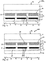
- Fig. 1a shows an intermediate product 100a in the manufacture of a multilayer body 100, which in the finished state in Fig. 1d is shown.
- the multi-layer body 100 after Fig. 1d comprises a carrier layer with a first side 11 and a second side 12.
- the carrier layer comprises a carrier film 1 and a functional layer 2.
- a first decorative layer 3 is arranged, which is formed in a first zone 8 first lacquer layer 31 and a replicating layer 4 comprises.
- a metal layer 5 is arranged in register with the first lacquer layer 3.
- a second decorative layer 7 arranged in register with the metal layer 5 is provided.
- a compensation layer 10 fills height differences between the replication layer 4, the metal layer 5 and the second decorative layer 7.
- the carrier film 1 is a preferably transparent plastic film having a thickness of between 8 ⁇ m and 125 ⁇ m, preferably in the range of 12 to 50 ⁇ m, more preferably in the range of 16 to 23 ⁇ m.
- the carrier film 1 can hereby be monoaxially or biaxially stretched. Further, it is also possible that the carrier film 1 not only of a layer, but also consists of several layers.
- the carrier film 1 it is possible for the carrier film 1 to have, in addition to a plastic carrier, for example a plastic film described above, a release layer which makes it possible to detach the layer structure consisting of the layers 2 to 6 and 10 from the plastic film, for example when using the multilayer body 100 as a hot stamping foil
- the functional layer 2 may comprise a release layer, e.g. of heat-melting material, which facilitates detachment of the carrier film 1 from the layers of the multilayer body 100, which are arranged on a side of the release layer 2 facing away from the carrier film 1.
- a release layer e.g. of heat-melting material
- This is particularly advantageous when the multilayer body 100 is formed as a transfer layer, as e.g. is used in a hot stamping process or an IMD process.
- the functional layer 2 contains, in addition to a release layer, a protective layer, e.g. a protective lacquer layer.
- the multilayer body 100 may be a section of a transfer film, for example a hot stamping film, which may be disposed on a substrate by means of an adhesive layer.
- the adhesive layer is preferably arranged on the side of the compensation layer 10 facing away from the carrier film 1.
- the adhesive layer may be a hot melt adhesive which melts upon thermal exposure and bonds the multi-layer body 100 to the surface of the substrate.
- the transparent, colored lacquer layer 31 is printed in the zone 8.
- Transparent means that the lacquer layer 31 in the visible wavelength range is at least partially transparent to radiation.
- Colored means that the varnish layer 31 shows a visible color impression with sufficient daylight.
- the lacquer layer 31 may in this case comprise a plurality of differently colored partial areas, such as in Fig. 1d indicated by different shading. As a result, a first motif can be provided. Next, the decorative layer 7, as in Fig. 1d indicated by different shades, forming different colored areas or areas with different optical properties, which in particular provide a second motif.
- Both the zones 8 printed with the lacquer layer 31 and the unprinted zones 9 of the functional layer 2 are covered by a replication layer 4, which preferably has any relief structures of the decorative layer 3 which are present, i. the differing levels in the printed 8 and unprinted zones 9, equalized.
- a thin metal layer 5 is arranged on the replication 4.
- a second decorative layer 7 is arranged.
- Both the zones 8 of the replication layer 4 covered with the metal layer 5 and the decorative layer 7 and the uncovered zones 9 of the replication layer 4 are covered with a compensating layer 10, the structures caused by the relief structures and the metal layer 5 arranged in some regions 8 (eg relief structure, different layer thicknesses) Height offset) equalized, ie covered and filled, so that the multi-layer body on the side facing away from the carrier film 1 side of the compensation layer 10 has a flat, substantially featureless surface.
- the compensation layer 10 has a similar refractive index as the replication layer 4, i. if the refractive index difference is less than about 0.15, then the zones of the relief structures in the replication layer 4 which are not covered by the metal layer 5 and are directly adjacent to the compensation layer 10 are optically extinguished because there are no optically detectable layer boundaries due to the similar refractive index of both layers between the replication layer 4 and the leveling layer 10 more are available.
- FIGS. 1a to 1c now show manufacturing stages of in Figure 1d shown multilayer body 100. Same elements as in Figure 1d are designated by the same reference numerals.
- FIG. 1a shows a first manufacturing stage 100a of the multilayer body 100, in which the carrier film 1 on a first side 11 comprises a functional layer 2, on which in turn a decorative layer 3 is arranged.
- One side of the functional layer 2 is adjacent to the carrier film 1, its other side to the decorative layer 3.
- the decorative layer 3 has a first zone 8, in which a lacquer layer 31 is formed, and a second zone 9, in which the lacquer layer 31 is not present is on.
- the lacquer layer 31 is printed on the functional layer 2, for example by screen printing, gravure printing or offset printing. The formation of the lacquer layer 31 in regions (in the first zones 8) results in a pattern-like configuration of the decorative layer 3.
- the lacquer layer 31 preferably has a layer thickness of 0.1 ⁇ m to 2 ⁇ m, more preferably of 0.3 ⁇ m to 1.5 ⁇ m.
- a replication layer 4 which is a component of the first decorative layer 3, is applied to the functional layer 2 and the varnish layer 31 arranged in regions (in the zones 8). It can be an organic Layer applied by conventional coating methods, such as printing, casting or spraying, in liquid form. The order of the replication layer 4 is provided here over the entire surface.
- the layer thickness of the replication layer 4 varies, as it compensates for the different levels of the decorative layer 3 comprising the printed first zone 8 and the unprinted second zone 9; In the first zone 8, the layer thickness of the replication layer 4 is thinner than in the second zone 9, so that the side facing away from the carrier layer 1 side of the replication layer 4 before the formation of relief structures in a flat, substantially featureless surface.
- the replication lacquer layer 9 preferably has a layer thickness of 0.1 ⁇ m to 3 ⁇ m, more preferably of 0.1 ⁇ m to 1.5 ⁇ m.
- an application of the replication layer 4 may also be provided only in a partial region of the multilayer body 100.
- the surface of the replication layer 4 can be structured in regions by known methods. For this purpose, for example, as a replication 4, a thermoplastic Replizierlack applied by printing, spraying or painting and molded a relief structure in the particular thermally curable / dry replicate 4 by means of a heated punch or a heated replicating roller.
- the replication layer 4 can also be a UV-curable replication lacquer which is structured, for example, by a replication roller and cured simultaneously and / or subsequently by means of UV radiation. However, the structuring can also be produced by UV irradiation through an exposure mask.
- the metal layer 5 is applied.
- the metal layer 5 may be formed, for example, as a vapor-deposited metal layer, for example of silver or aluminum.
- the order of the metal layer is provided here over the entire surface.
- an application may also be provided only in a partial region of the multilayer body 100, for example with the aid of a partially shielding vapor deposition mask.
- the metal layer preferably has a layer thickness of 20 nm to 70 nm.
- a photoactivatable resist layer 6 is applied on the metal layer 5, a photoactivatable resist layer 6 is applied.
- the resist layer 6 may be an organic layer which is applied in a liquid form by classical coating methods such as printing, casting or spraying. It can also be provided that the resist layer 6 is vapor-deposited or laminated as a dry film.
- the photoactivatable layer 6 can be, for example, a positive photoresist AZ Clariant or act of MICROPOSIT ® S1818 from Shipley 1512 in which a surface density of 0.1 g / m 2 to 10 g / m 2, preferably from 0.1 g / m 2 to 1 g / m 2 is applied to the layer 5 to be structured.
- the layer thickness depends on the desired resolution and the process. The order is provided here over the entire area. However, an application may also be provided only in a partial area of the multilayer body 100.
- FIG. 1b shows a second manufacturing stage 100b of the multi-layer body 100, in which the first manufacturing stage 100a of the multi-layer body 100 was irradiated and then developed.
- Electromagnetic radiation having a wavelength which is suitable for activating the photoactivatable resist layer 6 is produced from the second side 12 of the carrier film 1, ie the side of the carrier film 1 which lies opposite the side of the carrier film 1 coated with the resist layer 6, through the multilayer body 100d blasted.
- the irradiation serves to activate the photoactivatable resist layer 6 in the second zone 9, in which the decorative layer 3 has a higher transmittance than in the first zone 8.
- the intensity and duration of the exposure to the electromagnetic radiation is coordinated with the multilayer body 100a such that the radiation in the second zone 9 activates the multilayer body 100a photoactivatable resist layer 6 leads, however, does not lead to activation of the photoactivatable resist layer 6 in the printed with the resist layer 31 first zone 8. It has proven useful if the contrast between the first zone 8 and the second zone 9 caused by the lacquer layer 31 is greater than two. Furthermore, it has proven useful if the lacquer layer 31 are configured such that the radiation after passing through the entire multi-layer body 100a has a ratio of the transmittances, ie a contrast ratio of approximately 1: 2 between the first zone 8 and the second zone 9.
- the exposure is preferably carried out with an illuminance of 100 mW / cm 2 to 500 mW / cm 2 , preferably from 150 mW / cm 2 to 350 mW / cm 2 .
- a developer solution e.g. As solvents or alkalis, in particular a sodium carbonate solution or a sodium hydroxide solution applied to the side facing away from the carrier film 1 surface of the exposed photoactivatable resist layer 6.
- the exposed resist layer 6 in the second zone 9 has been removed.
- the resist layer 6 is obtained because the amount of radiation absorbed in these zones has not led to sufficient activation.
- the resist layer 6 thus formed of a positive photoresist.
- the more exposed zones 9 are soluble in the developer solution, eg the solvent.
- the unexposed or less exposed zones 8 are soluble in the developer solution.
- the metal layer 5 in the second zone 9 is removed by an etchant.
- the etchant may be, for example, an acid or alkali, for example NaOH (sodium hydroxide). or Na 2 CO 3 (sodium carbonate) in a concentration of 0.05% to 5%, preferably from 0.3% to 3%. In this way, the in FIG. 1b shown portions of the metal layer 5 is formed.
- the metal layer 5 can be structured in register with the first and second zones 8 and 9 defined by the lacquer layer 31 without additional technological effort.
- the mask being formed either as a separate unit, e.g. is present as a separate film or as a separate glass plate / glass roller, or as a subsequently printed layer, the problem arises that by previous, in particular thermally and / or mechanically consuming process steps, e.g.
- the first and second zones 8 and 9 defined by the lacquer layer 31 are used as a mask, wherein the lacquer layer 31 is applied in an early process step in the production of the multilayer body 100 as described above.
- the lacquer layer 31 is applied in an early process step in the production of the multilayer body 100 as described above.
- the tolerances or register accuracies in the method according to the invention lie only in the not absolutely exact course of the color edge of the defined by the lacquer layer 31 first and second zones 8 and 9 whose quality is determined by the particular printing method used, and are approximately in the micrometer range, and thus far below the resolution of the eye; ie the unarmed human eye can no longer perceive existing tolerances.
- the next, in Fig. 1c represented intermediate product 100c is obtained from the intermediate product 100b by a further, second decorative layer 7 on the covered by the structured layer 5 zones 8 and on the not covered by the structured layer 5 zones 9 of the replication layer 4, in particular partially applied.
- the second decorative layer 7 comprises at least one second photoactivatable resist layer.
- the second decorative layer 7 has two or more, in particular differently colored second resist layers.
- the second resist layers can also be printed in pattern form here.
- the second resist layers may also have a multilayer structure.
- the second resist layers may also be partially colorless transparent or translucent, ie have no coloration.
- the second resist layer 6 may be in the second resist layer, for example, a positive photoresist AZ 1512 from Clariant or MICROPOSIT ® S1818 from Shipley act, which in a surface density of 0.1 g / m 2 to 10 g / m 2, preferably from 0.5 g / m 2 to 1 g / m 2 is applied.
- the order is provided here over the entire area. However, an application may also be provided only in a partial area of the multilayer body 100. Since the second decorative layer 7 should at least partially be retained in the finished multi-layer body 100, dyes, pigments, nanoparticles or the like may additionally be incorporated into the lacquer in order to achieve an optical effect.
- the second decorative layer 7 is now also exposed from the side 12 of the carrier layer 1, for which purpose the parameters already described during the exposure of the first resist layer 6 can be used.
- Second decor layer 7 now the lacquer layer 31 and the metal layer 5 act together as a mask, so that the at least one resist layer of the second decorative layer 7 is exposed only in the zone 9, while the area covered by lacquer layer 31 and structured layer 5 remains unexposed.
- the second decorative layer 7 for developing with a developer solution, for. B. an alkali, in particular a sodium carbonate solution or a sodium hydroxide solution.
- a developer solution for. B. an alkali, in particular a sodium carbonate solution or a sodium hydroxide solution.
- the second resist layer is retained because the amount of radiation absorbed in these zones has not led to sufficient activation.
- this reverses as already described, so that the second resist layer is removed in the first zone 8 and is retained in the second zone 9.
- the in Figure 1d shown multilayer body 100 is made of the in FIG. 1 c illustrated manufacturing stage 100c of the multilayer body 100 formed by a compensation layer 10 on the arranged in the first zone 8, exposed second decorative layer 7 and on the disposed in the second zone 9, by removing the metal layer 5 and the first 6 and second resist layer exposed replication layer 4 is applied.
- the order of the leveling layer 10 is provided here over the entire surface.
- the compensating layer used is in particular a UV-crosslinked or heat-crosslinked lacquer.
- the compensating layer 10 is applied in the first zone 8 and the second zone 9 in each case in a different layer thickness, for example by knife coating, printing or spraying, so that the leveling layer 10 on its side facing away from the carrier layer 1 a flat, having substantially structureless surface.
- the layer thickness of the compensating layer 10 varies because it varies the levels of the metal layer 5 arranged in the first zone 8 and that exposed in the second zone 9 Replicating 4 compensated / equalized.
- the layer thickness of the compensation layer 10 is greater than the layer thickness of the metal layer 5 is selected in the first zone 8, so that the side facing away from the carrier layer 1 side of the compensation layer 10 has a flat surface.
- an application of the compensating layer 10 may also be provided only in a partial region of the multilayer body 100. It is possible for one or more further layers, for example an adhesion or adhesive layer, to be applied to the planar compensation layer 10.
- the first and second zones 8 and 9 defined by the lacquer layer 31 and by the metal layer 5 are used as a mask for structuring the second decorative layer 7.
- no additional tolerances and no additional tolerance fluctuations over the surface of the multi-layer body 100 occur, since the subsequent generation of a mask and thereby required register-accurate subsequent positioning of this independent of the previous process mask is avoided.
- a multi-layer body 100 is obtained, in which the lacquer layer 31 of the decorative layer 3, the metal layer 5 and the second decorative layer 7 are arranged in the perfect register.
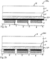
- Fig. 2d shows another multilayer body 200, which is produced by a variant of the method.
- the process steps and intermediates 200a, 200b and 200c are in the FIGS. 2a to 2c shown.
- the further multi-layer body 200 corresponds to the in Figure 1d Therefore, the same reference numerals are used for the same structures and functional elements.
- the multilayer body 200 also comprises a carrier layer with a first side 11 and a second side 12.
- the carrier layer comprises a carrier foil 1 and a functional layer 2.
- a first decorative layer 3 is arranged, which is formed by a replication layer 4.
- the decorative layer 3 may be formed of a plurality of layers and, for example, a colored layer and have a replication layer.
- a metal layer 5 is arranged on the replication layer 4, a metal layer 5 is arranged.
- a second decorative layer 7 arranged in register with the metal layer 5 is provided.
- An equalization layer 10 fills height differences between the replication layer 4, the metal layer 5 and the second decoration layer 7.
- the multi-layer body 200 differs from the multi-layer body 100 only in that the decorative layer 3 does not have separate lacquer areas 31, but is formed entirely from a colored replication lacquer which may contain dyes, pigments, UV-activatable substances, nanoparticles or the like or alternatively completely from one correspondingly colored lacquer layer and a transparent colorless Replizierlack is formed.
- a colored replication lacquer which may contain dyes, pigments, UV-activatable substances, nanoparticles or the like or alternatively completely from one correspondingly colored lacquer layer and a transparent colorless Replizierlack is formed.
- FIG. 2a shown intermediate 200a provided.
- a carrier foil 1 is provided with a functional layer 2 onto which the decor layer 3 is applied over the whole area.
- reliefs for example diffractive structures, can additionally be introduced into the replication layer 4 of the decorative layer 3.
- the replication layer 4 is then metallized over the entire surface in the manner already described.
- to be structured layer 5 now one or more, also differently colored resist layers comprising second decorative layer 7 is printed over part of the area, so that in the zone 8, the metal layer 5 is protected by the second decorative layer 7, while in the zone. 9 the metal layer 5 is not covered by the second decorative layer 7.
- the second decorative layer 7 comprises layers, in particular resist layers, which may contain dyes, pigments, UV-activatable substances, nanoparticles or the like.
- the second decorative layer 7 may be formed, for example, from a PVC-based paint.
- the intermediate product 200a of the multilayer body 200 is now treated with an etchant, in particular a sodium carbonate solution or a sodium hydroxide solution, which is applied to the side facing away from the carrier film 1 surface of the intermediate product 200a.
- an etchant in particular a sodium carbonate solution or a sodium hydroxide solution
- the liquor can dissolve the metal layer 5 in the zone 9, so that the metal layer 5 is removed in the zone 9. In this way it can be achieved that the metal layer 5 is formed in the perfect register to the second decorative layer 7.
- the second decorative layer 7 thus acts as an etch resist here.
- the intermediate product 200b is subsequently treated with a solvent, which should preferably have a flash point of more than 65 ° C.
- the solvent is chosen so that the second decorative layer 7 is insensitive to the solvent, while the material of the replication layer 4 can dissolve in the solvent.
- Suitable paints, in particular for the replication varnish 4, which have these properties are, for example, polyacrylates or polyacrylates in combination with cellulose derivatives.
- an equalization layer 10 is applied which compensates any existing relief structures in the replication layer 4, as well as the removed zones 9 of the replication layer 4 and the metal layer 5, so that a smooth surface of the multi-layer body 200 results.
- an equalization layer 10 is applied which compensates any existing relief structures in the replication layer 4, as well as the removed zones 9 of the replication layer 4 and the metal layer 5, so that a smooth surface of the multi-layer body 200 results.
- even more functional layers or the like can be applied.
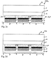
- Fig. 3e shows a further multi-layer body 300, which is produced by a variant of the method.
- the process steps and intermediates 300a, 300b, 300c and 300d are in the FIGS. 3a to 3d shown.
- the further multi-layer body 300 also corresponds to the in Fig. 1d and Fig. 2d shown multilayer bodies 100 and 200.
- the same reference numerals are used for the same structures and functional elements, therefore, the same reference numerals are used.
- the multilayer body 300 also comprises a carrier layer with a first side 11 and a second side 12, which comprises a carrier foil 1 and a functional layer 2.
- a replication layer 4 is arranged, which is colored and at the same time acts as a first decorative layer 3.
- the decorative layer 3 may also be multi-layered and, for example, have a colored layer and a replication layer.
- a metal layer 5 in register with the first decorative layer 3 and a second decorative layer 7 arranged in register with the metal layer 5 are provided. Height differences of the replication layer 4, the metal layer 5 and the second decorative layer 7 are filled by a leveling layer 10.
- Multi-layer body 300 of the multi-layer body 100 differs Multi-layer body 300 of the multi-layer body 100 only in that the decorative layer 3 does not have separate lacquer areas 31, but is formed entirely from a colored replicate lacquer which may contain dyes, pigments, UV-activatable substances, nanoparticles or the like, or alternatively completely from a suitably colored lacquer layer and a transparent colorless replicate varnish is formed.
- a colored replicate lacquer which may contain dyes, pigments, UV-activatable substances, nanoparticles or the like, or alternatively completely from a suitably colored lacquer layer and a transparent colorless replicate varnish is formed.
- Fig. 3a shows a first intermediate product 300a in the production of the multi-layer body 300 according to a variant of the method.
- a carrier foil 1 is first provided with a functional layer 2 on which the decor layer 3 is applied over the whole area.
- reliefs for example diffractive structures, can additionally be introduced into the replication layer 4 of the decorative layer 3.
- the replication layer 4 is then metallized over the entire surface in the manner already described. On the metal layer 5 thus obtained, a resist 6 is now applied over the entire surface.
- the mask 13 On the side facing away from the carrier sheet 1 of the resist 6, a mask 13 is now placed.
- the mask 13 here is a separate part, ie it is not formed by structures of the multilayer body 300 itself.
- the mask includes zones 8 that are opaque to the electromagnetic radiation used to expose the photoactivatable resist 6, and zones 9 that are transparent to said radiation. Since the mask 13 is arranged on the side of the resist 6 facing away from the carrier film 1, the exposure of the resist 6 must likewise take place from this side, ie it can not take place from the side of the carrier film 1, as in the production of the multilayer body 100.
- a combination of a positive resist 6 with a positive mask 13 is used.
- the resist 6 is therefore protected in the zone 8 by the mask and exposed only in the zone 9.
- the resist 6 is thus removed during the development, so that the metal layer 5 is exposed in the zone 5 and is removed by the etchant in the subsequent etching step.
- a negative mask can also be used in combination with a negative resist.
- the in Fig. 3b obtained intermediate product 300b, in which the structured layer is present only in the zones 8, while in the zones 9, the replication layer 4 is exposed.
- the resist 6 is still present on the surface of the metal layer 5 facing away from the carrier foil 1.
- the resist 6 is removed by solvent treatment ("stripped").
- solvent treatment For this purpose, the comments to Fig. 2c and 2d directed. This can also be done in the manner already described in the production of the multilayer body 100.
- the replication layer 4 in the zone 9, in which it is not protected by the metal layer 5, is removed at the same time.
- a second decorative layer 7 is then applied over the entire surface of the metal layer 5 or the exposed zones 9 of the functional layer 2, so that the in Fig. 3d shown intermediate 300d is obtained.
- the second decorative layer 7 comprises at least one layer of a photoactivatable resist, preferably two or more photoactivatable, differently colored layers, and at the same time acts as a leveling layer, which compensates the height differences due to the partial removal the metal layer 5 and the replication layer 4 compensates.
- the second decorative layer 7 remains partially in the finished multi-layer body and assumes an optical function there.
- the second decorative layer 7 therefore comprises at least one layer dyed with dyes, pigments, UV-active substances, nanoparticles or the like.
- the zone 8 formed by the remaining decorative layer 3 and the metal layer 5 is intransparent for the electromagnetic radiation used to expose the resist of the second decorative layer 7.
- an exposure of the resist of the second decorative layer 7 can now be carried out from the side of the carrier film and the resist can subsequently be developed in the manner already described. Since the remaining decorative layer 3 acts together with the metal layer 5 as a mask, the resist is thus exposed only in the zone 9. When using a positive resist, the resist is thus removed in the zone 9 during development, so that it remains only where it rests directly on the metal layer 5.
- the zone 9, in which the resist of the second decorative layer 7 has been removed is provided with a leveling layer 10 in order to compensate for the height differences.
- a crosslinked, transparent sealing layer 14 can also be applied to the side of the multilayer body 300 facing away from the carrier film 1 in order to protect its surface against mechanical damage.
- Fig. 4d shows a further multi-layer body 400, which is produced by a variant of the method.
- the process steps and intermediates 400a, 400b and 400c are in the FIGS. 4a to 4c shown.
- the multilayer body 400 is different from that in FIG Fig. 1a shown multi-layer body 100 only in that the second decorative layer 7 is formed in a first portion of a photoactivatable resist layer and in a second portion of a partially applied etching resist layer.
- the decorative layer 3 may have first zones 8 and / or second zones 9 as well as in the first subarea.
- the structure of the multilayer body 400 corresponds to the multilayer body 100 in FIGS Fig. 1a to 1d and the method steps described there are also carried out in order to produce a multilayer body 400, as described in US Pat Fig. 4d shown in the first section.
- the second subarea is now provided in which, instead of the photoactivatable resist layer 6, an etching resist layer 15 is partially applied.
- the motif or the external shape of the etching resist layer 15 is intended to determine the motif or the external shape of the partial metallization to be achieved.
- the etching resist layer 15 may for example consist of a PVC-based lacquer and be colored by means of pigments and / or dyes or be colorless transparent or translucent.
- the metal layer 5 in the second zone 9 is removed by an etchant.
- the etchant may be, for example, an acid or alkali, for example NaOH (sodium hydroxide) or Na 2 CO 3 (sodium carbonate) in a concentration of 0.05% to 5%, preferably of 0.3% to 3%. In this way, the in FIG. 4b shown portions of the metal layer 5 is formed.
- the remaining areas of the resist layer 6 are also removed ("stripping"). In this case, however, the etching resist layer 15 is maintained on the metal layer 5.
- the metal layer 5 can be structured in register with the first and second zones 8 and 9 defined by the lacquer layer 31 without additional technological effort in the first partial area and in register with the etching resist layer 15 in the second partial area.
- a further, second decorative layer 7 is applied to the zones 8 covered by the structured layer 5 and to the zones 9 of the replication layer 4 not covered by the structured layer 5.
- the second decorative layer 7 comprises at least one second photoactivatable resist layer.
- the second decorative layer 7 has two or more, in particular differently colored second resist layers.
- the second resist layers can also be printed in pattern form here.
- the etching resist layer 15 still present in the second subregion likewise forms a part of the decorative layer 7.
- the application of the decorative layer 7 in the first portion may also be omitted, so that in the first portion of the metal layer 5 is present without coating and in the second portion with the applied etching resist layer 15.
- a coloring of the metal layer 5 by means of colored etching resist layer 15th take place only in the second subarea and in the first subregion, the metal layer 5 is true to register the first Decorative layer before, however, is not colored on the side facing away from the first decorative layer and in the case of aluminum silver glossy reflective.
- the decorative layer 7 is exposed in the first part, developed and partially removed.
- a leveling layer 10 is formed on the exposed second decorative layer 7 arranged in the first zone 8 as well as on the replication layer 4 arranged in the second zone 9 and exposed by removing the metal layer 5 and the first 6 and second resist layers is applied.
- the order of the leveling layer 10 is provided here over the entire surface.
- the leveling layer 10 may be single or multi-layered or omitted. It is possible for a bonding layer (adhesive layer) (not shown here) to be applied to the side of the leveling layer 10 facing away from the carrier layer, which may also have a multilayer structure.
Landscapes
- Engineering & Computer Science (AREA)
- Manufacturing & Machinery (AREA)
- Chemical & Material Sciences (AREA)
- General Chemical & Material Sciences (AREA)
- Chemical Kinetics & Catalysis (AREA)
- Electromagnetism (AREA)
- Toxicology (AREA)
- General Health & Medical Sciences (AREA)
- Health & Medical Sciences (AREA)
- Physics & Mathematics (AREA)
- Life Sciences & Earth Sciences (AREA)
- Wood Science & Technology (AREA)
- Laminated Bodies (AREA)
- Diffracting Gratings Or Hologram Optical Elements (AREA)
- Credit Cards Or The Like (AREA)
- Holo Graphy (AREA)
- Production Of Multi-Layered Print Wiring Board (AREA)
Priority Applications (3)
| Application Number | Priority Date | Filing Date | Title |
|---|---|---|---|
| RS20170445A RS55994B1 (sr) | 2013-06-28 | 2014-06-26 | Postupak za izradu višeslojnog tela kao i višeslojno telo |
| PL14733628T PL3013598T3 (pl) | 2013-06-28 | 2014-06-26 | Sposób wytwarzania korpusu wielowarstwowego oraz korpus wielowarstwowy |
| HRP20170741TT HRP20170741T1 (hr) | 2013-06-28 | 2017-05-18 | Postupak za proizvodnju višeslojnog tijela i višeslojno tijelo |
Applications Claiming Priority (2)
| Application Number | Priority Date | Filing Date | Title |
|---|---|---|---|
| DE102013106827.8A DE102013106827A1 (de) | 2013-06-28 | 2013-06-28 | Verfahren zur Herstellung eines Mehrschichtkörpers sowie Mehrschichtkörper |
| PCT/EP2014/063623 WO2014207165A1 (de) | 2013-06-28 | 2014-06-26 | Verfahren zur herstellung eines mehrschichtkörpers sowie mehrschichtkörper |
Publications (2)
| Publication Number | Publication Date |
|---|---|
| EP3013598A1 EP3013598A1 (de) | 2016-05-04 |
| EP3013598B1 true EP3013598B1 (de) | 2017-03-01 |
Family
ID=51022871
Family Applications (1)
| Application Number | Title | Priority Date | Filing Date |
|---|---|---|---|
| EP14733628.3A Active EP3013598B1 (de) | 2013-06-28 | 2014-06-26 | Verfahren zur herstellung eines mehrschichtkörpers sowie mehrschichtkörper |
Country Status (16)
| Country | Link |
|---|---|
| US (2) | US10029505B2 (hr) |
| EP (1) | EP3013598B1 (hr) |
| JP (2) | JP6478230B2 (hr) |
| CN (1) | CN105431302B (hr) |
| AU (1) | AU2014301007B2 (hr) |
| BR (1) | BR112015032480B1 (hr) |
| CA (1) | CA2926821C (hr) |
| DE (1) | DE102013106827A1 (hr) |
| ES (1) | ES2625750T3 (hr) |
| HR (1) | HRP20170741T1 (hr) |
| HU (1) | HUE034529T2 (hr) |
| MX (1) | MX346389B (hr) |
| PL (1) | PL3013598T3 (hr) |
| RS (1) | RS55994B1 (hr) |
| RU (1) | RU2664356C2 (hr) |
| WO (1) | WO2014207165A1 (hr) |
Families Citing this family (20)
| Publication number | Priority date | Publication date | Assignee | Title |
|---|---|---|---|---|
| DE102013106827A1 (de) * | 2013-06-28 | 2014-12-31 | Leonhard Kurz Stiftung & Co. Kg | Verfahren zur Herstellung eines Mehrschichtkörpers sowie Mehrschichtkörper |
| DE102013113283A1 (de) * | 2013-11-29 | 2015-06-03 | Leonhard Kurz Stiftung & Co. Kg | Mehrschichtkörper und Verfahren zu dessen Herstellung |
| DE102015104416A1 (de) * | 2015-03-24 | 2016-09-29 | Leonhard Kurz Stiftung & Co. Kg | Mehrschichtkörper und Verfahren zu dessen Herstellung |
| DE102015106800B4 (de) * | 2015-04-30 | 2021-12-30 | Leonhard Kurz Stiftung & Co. Kg | Verfahren zum Herstellen eines Mehrschichtkörpers |
| GB2539390B (en) * | 2015-06-10 | 2018-07-25 | De La Rue Int Ltd | Security devices and methods of manufacture thereof |
| DE102015112909B3 (de) * | 2015-08-05 | 2017-02-09 | Leonhard Kurz Stiftung & Co. Kg | Verfahren und Vorrichtung zum Herstellen einer Mehrschichtfolie |
| DE102015120535A1 (de) | 2015-11-26 | 2017-06-01 | Leibniz-Institut für Oberflächenmodifizierung e.V. | Vorrichtung und Verfahren zur Herstellung einer beidseitig mikrostrukturierten Folie |
| GB2549724B (en) | 2016-04-26 | 2019-12-11 | De La Rue Int Ltd | Security devices and methods of manufacturing image patterns for security devices |
| GB2551555B (en) * | 2016-06-22 | 2018-09-26 | De La Rue Int Ltd | Methods of manufacturing an image pattern for a security device |
| DE102016009024A1 (de) † | 2016-07-25 | 2018-01-25 | Giesecke+Devrient Currency Technology Gmbh | Sicherheitspapier, Sicherheitselement und Wertdokument |
| EP3576956A1 (en) | 2017-02-02 | 2019-12-11 | Fedrigoni S.p.A. | Double metal security element having transparent pattern |
| EP3633422B1 (en) * | 2017-05-22 | 2023-11-22 | Toppan Printing Co., Ltd. | Information recording body and individual certifying body |
| EP4112327A1 (en) * | 2017-08-23 | 2023-01-04 | Toppan Printing Co., Ltd. | Laminates identification documents, and methods for verifying identification documents |
| AT520293B1 (de) * | 2017-10-04 | 2019-03-15 | Formfinder Software Gmbh | Folie |
| CN108254937B (zh) * | 2017-12-19 | 2021-03-23 | 浙江理工大学 | 一种双成像方法、装置及其应用 |
| DE102018004054A1 (de) * | 2018-05-18 | 2019-11-21 | Giesecke+Devrient Currency Technology Gmbh | Herstellungsverfahren für ein Sicherheitselement |
| DE102018125312A1 (de) * | 2018-10-12 | 2020-04-16 | Leonhard Kurz Stiftung & Co. Kg | Verfahren zur Herstellung eines dekorierten, mineralischen Verbundkörpers, dekorierter, mineralischer Verbundkörper und Verwendung einer Mehrschichtfolie |
| DE102019115391A1 (de) * | 2019-06-06 | 2020-12-10 | Leonhard Kurz Stiftung & Co. Kg | Durchsichtsicherheitselement |
| RU208267U1 (ru) * | 2021-07-01 | 2021-12-13 | Олег Умарович Айбазов | Банковская карта |
| WO2023182438A1 (ja) * | 2022-03-23 | 2023-09-28 | 凸版印刷株式会社 | 化粧シートの製造方法及び化粧シート |
Family Cites Families (21)
| Publication number | Priority date | Publication date | Assignee | Title |
|---|---|---|---|---|
| US4564571A (en) * | 1983-03-31 | 1986-01-14 | Jun Masaki | Transfer sheet with color pattern having metallic luster, and method of manufacturing said sheet |
| JPS59182782A (ja) | 1983-03-31 | 1984-10-17 | Jun Masaki | アルミニウム蒸着金属層による任意模様の転写シ−トの製法 |
| CA1228225A (en) * | 1984-11-09 | 1987-10-20 | National Research Council Of Canada | Method of manufacturing an optical interference authenticating device |
| JPH0635237B2 (ja) | 1989-07-18 | 1994-05-11 | 森山印刷株式会社 | 転写シートの製造法 |
| US5289547A (en) | 1991-12-06 | 1994-02-22 | Ppg Industries, Inc. | Authenticating method |
| US5470644A (en) | 1994-04-21 | 1995-11-28 | Durant; David | Apparatus and method for fabrication of printed circuit boards |
| DE19813314A1 (de) | 1998-03-26 | 1999-09-30 | Kurz Leonhard Fa | Prägefolie, insbesondere Heissprägefolie |
| DE10218897A1 (de) | 2002-04-26 | 2003-11-06 | Giesecke & Devrient Gmbh | Sicherheitselement und Verfahren zu seiner Herstellung |
| US7535641B2 (en) | 2002-05-14 | 2009-05-19 | Leonhard Kurz Gmbh & Co., Kg | Optically variable element comprising a partial transparent element |
| DE10356146A1 (de) | 2003-12-02 | 2005-06-30 | Giesecke & Devrient Gmbh | Datenträger und Verfahren zu seiner Herstellung |
| DE102005006277B4 (de) | 2005-02-10 | 2007-09-20 | Ovd Kinegram Ag | Verfahren zur Herstellung eines Mehrschichtkörpers |
| DE102005006231B4 (de) | 2005-02-10 | 2007-09-20 | Ovd Kinegram Ag | Verfahren zur Herstellung eines Mehrschichtkörpers |
| DE102005034671A1 (de) * | 2005-07-25 | 2007-02-01 | Giesecke & Devrient Gmbh | Sicherheitselement und Verfahren zu seiner Herstellung |
| US20090220750A1 (en) | 2006-02-28 | 2009-09-03 | Contra Vision Limited | Partial Printing Of A Substrate Using Metallization |
| DE102007039996B4 (de) | 2007-02-07 | 2020-09-24 | Leonhard Kurz Stiftung & Co. Kg | Sicherheitselement für ein Sicherheitsdokument und Verfahren zu seiner Herstellung |
| DE102008013073B4 (de) * | 2008-03-06 | 2011-02-03 | Leonhard Kurz Stiftung & Co. Kg | Verfahren zur Herstellung eines Folienelements und Folienelement |
| DE102008031325A1 (de) | 2008-07-02 | 2010-01-07 | Giesecke & Devrient Gmbh | Sicherheitselement sowie Verfahren zu seiner Herstellung |
| DE102008036481A1 (de) * | 2008-08-05 | 2010-02-11 | Giesecke & Devrient Gmbh | Verfahren zur Herstellung von Sicherheitselementen mit zueinander gepasserten Motiven |
| DE102009033762A1 (de) * | 2009-07-17 | 2011-01-27 | Leonhard Kurz Stiftung & Co. Kg | Verfahren zur Herstellung eines Mehrschichtkörpers sowie Mehrschichtkörper |
| JP2012242411A (ja) | 2011-05-16 | 2012-12-10 | Dainippon Printing Co Ltd | ホログラムシート |
| DE102013106827A1 (de) * | 2013-06-28 | 2014-12-31 | Leonhard Kurz Stiftung & Co. Kg | Verfahren zur Herstellung eines Mehrschichtkörpers sowie Mehrschichtkörper |
-
2013
- 2013-06-28 DE DE102013106827.8A patent/DE102013106827A1/de active Pending
-
2014
- 2014-06-26 CN CN201480042836.6A patent/CN105431302B/zh active Active
- 2014-06-26 WO PCT/EP2014/063623 patent/WO2014207165A1/de active Application Filing
- 2014-06-26 US US14/900,646 patent/US10029505B2/en active Active
- 2014-06-26 CA CA2926821A patent/CA2926821C/en active Active
- 2014-06-26 HU HUE14733628A patent/HUE034529T2/en unknown
- 2014-06-26 ES ES14733628.3T patent/ES2625750T3/es active Active
- 2014-06-26 EP EP14733628.3A patent/EP3013598B1/de active Active
- 2014-06-26 JP JP2016522519A patent/JP6478230B2/ja active Active
- 2014-06-26 RS RS20170445A patent/RS55994B1/sr unknown
- 2014-06-26 MX MX2015017592A patent/MX346389B/es active IP Right Grant
- 2014-06-26 RU RU2016102641A patent/RU2664356C2/ru active
- 2014-06-26 AU AU2014301007A patent/AU2014301007B2/en active Active
- 2014-06-26 BR BR112015032480-0A patent/BR112015032480B1/pt active IP Right Grant
- 2014-06-26 PL PL14733628T patent/PL3013598T3/pl unknown
-
2017
- 2017-05-18 HR HRP20170741TT patent/HRP20170741T1/hr unknown
-
2018
- 2018-06-25 US US16/016,919 patent/US10926571B2/en active Active
- 2018-11-22 JP JP2018219403A patent/JP6790334B2/ja active Active
Also Published As
| Publication number | Publication date |
|---|---|
| JP2016533921A (ja) | 2016-11-04 |
| US20160185150A1 (en) | 2016-06-30 |
| HUE034529T2 (en) | 2018-02-28 |
| AU2014301007B2 (en) | 2017-11-30 |
| MX2015017592A (es) | 2016-04-07 |
| RU2664356C2 (ru) | 2018-08-16 |
| AU2014301007A1 (en) | 2016-01-28 |
| CN105431302A (zh) | 2016-03-23 |
| PL3013598T3 (pl) | 2017-08-31 |
| BR112015032480B1 (pt) | 2021-12-21 |
| EP3013598A1 (de) | 2016-05-04 |
| JP6478230B2 (ja) | 2019-03-06 |
| MX346389B (es) | 2017-03-17 |
| JP6790334B2 (ja) | 2020-11-25 |
| US10926571B2 (en) | 2021-02-23 |
| JP2019073019A (ja) | 2019-05-16 |
| BR112015032480A2 (pt) | 2017-07-25 |
| RU2016102641A3 (hr) | 2018-05-29 |
| RU2016102641A (ru) | 2017-08-03 |
| HRP20170741T1 (hr) | 2017-07-28 |
| US20180304667A1 (en) | 2018-10-25 |
| CA2926821A1 (en) | 2014-12-31 |
| ES2625750T3 (es) | 2017-07-20 |
| RS55994B1 (sr) | 2017-09-29 |
| US10029505B2 (en) | 2018-07-24 |
| WO2014207165A1 (de) | 2014-12-31 |
| CN105431302B (zh) | 2017-08-08 |
| CA2926821C (en) | 2022-05-17 |
| DE102013106827A1 (de) | 2014-12-31 |
Similar Documents
| Publication | Publication Date | Title |
|---|---|---|
| EP3013598B1 (de) | Verfahren zur herstellung eines mehrschichtkörpers sowie mehrschichtkörper | |
| EP2454100B1 (de) | Verfahren zur herstellung eines mehrschichtkörpers sowie mehrschichtkörper | |
| EP2049345B1 (de) | Verfahren zur herstellung eines mehrschichtkörpers sowie mehrschichtkörper | |
| EP2860041B1 (de) | Verfahren zur Herstellung eines Mehrschichtkörpers sowie Mehrschichtkörper | |
| EP3339052A1 (de) | Verfahren zur dekoration von oberflächen | |
| DE102018103236A1 (de) | Sicherheitselement und Verfahren zur Herstellung eines Sicherheitselements | |
| EP2874823B1 (de) | Verfahren zur herstellung eines mehrschichtigen sicherheitselements | |
| EP4112324B1 (de) | Sicherheitssubstrat und daraus hergestelltes wertdokument | |
| EP3894232B1 (de) | Verfahren zur herstellung eines folienzwischenprodukts, folienzwischenprodukt sowie verfahren zur herstellung eines produkts | |
| DE102015104416A1 (de) | Mehrschichtkörper und Verfahren zu dessen Herstellung | |
| EP3980275A1 (de) | Durchsichtsicherheitselement | |
| DE102016109633A1 (de) | Verfahren zur Herstellung einer Volumenhologrammfolie mit als Übertragungsabschnitte ausgebildeten Sicherheitselementen | |
| DE102010025278A1 (de) | Verfahren zur Dekoration von Oberflächen | |
| DE102020005912A1 (de) | Verfahren zum Herstellen eines optisch variablen Sicherheitselements | |
| EP3486092A1 (de) | Verfahren zum herstellen eines sicherheitselementes |
Legal Events
| Date | Code | Title | Description |
|---|---|---|---|
| PUAI | Public reference made under article 153(3) epc to a published international application that has entered the european phase |
Free format text: ORIGINAL CODE: 0009012 |
|
| 17P | Request for examination filed |
Effective date: 20160113 |
|
| AK | Designated contracting states |
Kind code of ref document: A1 Designated state(s): AL AT BE BG CH CY CZ DE DK EE ES FI FR GB GR HR HU IE IS IT LI LT LU LV MC MK MT NL NO PL PT RO RS SE SI SK SM TR |
|
| AX | Request for extension of the european patent |
Extension state: BA ME |
|
| 111L | Licence recorded |
Designated state(s): AL AT BE BG CH CY CZ DE DK EE ES FI FR GB GR HR HU IE IS IT LT LU LV MC MK MT NL NO PL PT RO RS SE SI SK SM TR Name of requester: THE GOVERNOR AND COMPANY OF THE BANK OF ENGLAND, G Effective date: 20160311 |
|
| REG | Reference to a national code |
Ref country code: FR Ref legal event code: EL |
|
| DAX | Request for extension of the european patent (deleted) | ||
| GRAP | Despatch of communication of intention to grant a patent |
Free format text: ORIGINAL CODE: EPIDOSNIGR1 |
|
| STAA | Information on the status of an ep patent application or granted ep patent |
Free format text: STATUS: GRANT OF PATENT IS INTENDED |
|
| INTG | Intention to grant announced |
Effective date: 20161103 |
|
| GRAS | Grant fee paid |
Free format text: ORIGINAL CODE: EPIDOSNIGR3 |
|
| GRAA | (expected) grant |
Free format text: ORIGINAL CODE: 0009210 |
|
| STAA | Information on the status of an ep patent application or granted ep patent |
Free format text: STATUS: THE PATENT HAS BEEN GRANTED |
|
| 111L | Licence recorded |
Designated state(s): AL AT BE BG CH CY CZ DE DK EE ES FI FR GB GR HR HU IE IS IT LT LU LV MC MK MT NL NO PL PT RO RS SE SI SK SM TR Name of requester: THE GOVERNOR AND COMPANY OF THE BANK OF ENGLAND, G Effective date: 20160311 |
|
| AK | Designated contracting states |
Kind code of ref document: B1 Designated state(s): AL AT BE BG CH CY CZ DE DK EE ES FI FR GB GR HR HU IE IS IT LI LT LU LV MC MK MT NL NO PL PT RO RS SE SI SK SM TR |
|
| REG | Reference to a national code |
Ref country code: GB Ref legal event code: FG4D Free format text: NOT ENGLISH |
|
| REG | Reference to a national code |
Ref country code: AT Ref legal event code: REF Ref document number: 870816 Country of ref document: AT Kind code of ref document: T Effective date: 20170315 Ref country code: CH Ref legal event code: PK Free format text: ERGAENZUNG LIZENZEINTRAG: NICHT AUSSCHLIESSLICHE LIZENZ Ref country code: CH Ref legal event code: EP |
|
| REG | Reference to a national code |
Ref country code: IE Ref legal event code: FG4D Free format text: LANGUAGE OF EP DOCUMENT: GERMAN |
|
| REG | Reference to a national code |
Ref country code: DE Ref legal event code: R096 Ref document number: 502014002871 Country of ref document: DE |
|
| REG | Reference to a national code |
Ref country code: CH Ref legal event code: NV Representative=s name: FIAMMENGHI-FIAMMENGHI, CH |
|
| REG | Reference to a national code |
Ref country code: HR Ref legal event code: TUEP Ref document number: P20170741 Country of ref document: HR |
|
| REG | Reference to a national code |
Ref country code: DK Ref legal event code: T3 Effective date: 20170523 |
|
| REG | Reference to a national code |
Ref country code: SE Ref legal event code: TRGR |
|
| REG | Reference to a national code |
Ref country code: FR Ref legal event code: PLFP Year of fee payment: 4 |
|
| REG | Reference to a national code |
Ref country code: NL Ref legal event code: MP Effective date: 20170301 |
|
| REG | Reference to a national code |
Ref country code: LT Ref legal event code: MG4D |
|
| REG | Reference to a national code |
Ref country code: ES Ref legal event code: FG2A Ref document number: 2625750 Country of ref document: ES Kind code of ref document: T3 Effective date: 20170720 |
|
| REG | Reference to a national code |
Ref country code: HR Ref legal event code: T1PR Ref document number: P20170741 Country of ref document: HR |
|
| PG25 | Lapsed in a contracting state [announced via postgrant information from national office to epo] |
Ref country code: FI Free format text: LAPSE BECAUSE OF FAILURE TO SUBMIT A TRANSLATION OF THE DESCRIPTION OR TO PAY THE FEE WITHIN THE PRESCRIBED TIME-LIMIT Effective date: 20170301 Ref country code: LT Free format text: LAPSE BECAUSE OF FAILURE TO SUBMIT A TRANSLATION OF THE DESCRIPTION OR TO PAY THE FEE WITHIN THE PRESCRIBED TIME-LIMIT Effective date: 20170301 Ref country code: NO Free format text: LAPSE BECAUSE OF FAILURE TO SUBMIT A TRANSLATION OF THE DESCRIPTION OR TO PAY THE FEE WITHIN THE PRESCRIBED TIME-LIMIT Effective date: 20170601 Ref country code: GR Free format text: LAPSE BECAUSE OF FAILURE TO SUBMIT A TRANSLATION OF THE DESCRIPTION OR TO PAY THE FEE WITHIN THE PRESCRIBED TIME-LIMIT Effective date: 20170602 |
|
| PG25 | Lapsed in a contracting state [announced via postgrant information from national office to epo] |
Ref country code: BG Free format text: LAPSE BECAUSE OF FAILURE TO SUBMIT A TRANSLATION OF THE DESCRIPTION OR TO PAY THE FEE WITHIN THE PRESCRIBED TIME-LIMIT Effective date: 20170601 Ref country code: LV Free format text: LAPSE BECAUSE OF FAILURE TO SUBMIT A TRANSLATION OF THE DESCRIPTION OR TO PAY THE FEE WITHIN THE PRESCRIBED TIME-LIMIT Effective date: 20170301 |
|
| PG25 | Lapsed in a contracting state [announced via postgrant information from national office to epo] |
Ref country code: NL Free format text: LAPSE BECAUSE OF FAILURE TO SUBMIT A TRANSLATION OF THE DESCRIPTION OR TO PAY THE FEE WITHIN THE PRESCRIBED TIME-LIMIT Effective date: 20170301 |
|
| PG25 | Lapsed in a contracting state [announced via postgrant information from national office to epo] |
Ref country code: SK Free format text: LAPSE BECAUSE OF FAILURE TO SUBMIT A TRANSLATION OF THE DESCRIPTION OR TO PAY THE FEE WITHIN THE PRESCRIBED TIME-LIMIT Effective date: 20170301 Ref country code: RO Free format text: LAPSE BECAUSE OF FAILURE TO SUBMIT A TRANSLATION OF THE DESCRIPTION OR TO PAY THE FEE WITHIN THE PRESCRIBED TIME-LIMIT Effective date: 20170301 Ref country code: EE Free format text: LAPSE BECAUSE OF FAILURE TO SUBMIT A TRANSLATION OF THE DESCRIPTION OR TO PAY THE FEE WITHIN THE PRESCRIBED TIME-LIMIT Effective date: 20170301 |
|
| REG | Reference to a national code |
Ref country code: DE Ref legal event code: R026 Ref document number: 502014002871 Country of ref document: DE |
|
| PG25 | Lapsed in a contracting state [announced via postgrant information from national office to epo] |
Ref country code: PT Free format text: LAPSE BECAUSE OF FAILURE TO SUBMIT A TRANSLATION OF THE DESCRIPTION OR TO PAY THE FEE WITHIN THE PRESCRIBED TIME-LIMIT Effective date: 20170703 Ref country code: SM Free format text: LAPSE BECAUSE OF FAILURE TO SUBMIT A TRANSLATION OF THE DESCRIPTION OR TO PAY THE FEE WITHIN THE PRESCRIBED TIME-LIMIT Effective date: 20170301 Ref country code: IS Free format text: LAPSE BECAUSE OF FAILURE TO SUBMIT A TRANSLATION OF THE DESCRIPTION OR TO PAY THE FEE WITHIN THE PRESCRIBED TIME-LIMIT Effective date: 20170701 |
|
| PLBI | Opposition filed |
Free format text: ORIGINAL CODE: 0009260 |
|
| PLAX | Notice of opposition and request to file observation + time limit sent |
Free format text: ORIGINAL CODE: EPIDOSNOBS2 |
|
| 26 | Opposition filed |
Opponent name: GIESECKE+DEVRIENT CURRENCY TECHNOLOGY GMBH Effective date: 20171127 |
|
| PG25 | Lapsed in a contracting state [announced via postgrant information from national office to epo] |
Ref country code: MC Free format text: LAPSE BECAUSE OF FAILURE TO SUBMIT A TRANSLATION OF THE DESCRIPTION OR TO PAY THE FEE WITHIN THE PRESCRIBED TIME-LIMIT Effective date: 20170301 |
|
| PG25 | Lapsed in a contracting state [announced via postgrant information from national office to epo] |
Ref country code: SI Free format text: LAPSE BECAUSE OF FAILURE TO SUBMIT A TRANSLATION OF THE DESCRIPTION OR TO PAY THE FEE WITHIN THE PRESCRIBED TIME-LIMIT Effective date: 20170301 |
|
| REG | Reference to a national code |
Ref country code: HU Ref legal event code: AG4A Ref document number: E034529 Country of ref document: HU |
|
| PLBB | Reply of patent proprietor to notice(s) of opposition received |
Free format text: ORIGINAL CODE: EPIDOSNOBS3 |
|
| REG | Reference to a national code |
Ref country code: IE Ref legal event code: MM4A |
|
| PG25 | Lapsed in a contracting state [announced via postgrant information from national office to epo] |
Ref country code: IE Free format text: LAPSE BECAUSE OF NON-PAYMENT OF DUE FEES Effective date: 20170626 Ref country code: LU Free format text: LAPSE BECAUSE OF NON-PAYMENT OF DUE FEES Effective date: 20170626 |
|
| REG | Reference to a national code |
Ref country code: BE Ref legal event code: MM Effective date: 20170630 |
|
| REG | Reference to a national code |
Ref country code: FR Ref legal event code: PLFP Year of fee payment: 5 |
|
| PG25 | Lapsed in a contracting state [announced via postgrant information from national office to epo] |
Ref country code: BE Free format text: LAPSE BECAUSE OF NON-PAYMENT OF DUE FEES Effective date: 20170630 |
|
| REG | Reference to a national code |
Ref country code: HR Ref legal event code: ODRP Ref document number: P20170741 Country of ref document: HR Payment date: 20190619 Year of fee payment: 6 |
|
| PG25 | Lapsed in a contracting state [announced via postgrant information from national office to epo] |
Ref country code: CY Free format text: LAPSE BECAUSE OF FAILURE TO SUBMIT A TRANSLATION OF THE DESCRIPTION OR TO PAY THE FEE WITHIN THE PRESCRIBED TIME-LIMIT Effective date: 20170301 |
|
| REG | Reference to a national code |
Ref country code: CH Ref legal event code: PK Free format text: BERICHTIGUNGEN |
|
| RIC2 | Information provided on ipc code assigned after grant |
Ipc: B42D 25/41 20140101AFI20191021BHEP Ipc: B42D 25/378 20140101ALI20191021BHEP Ipc: B42D 25/45 20140101ALI20191021BHEP Ipc: B42D 25/387 20140101ALI20191021BHEP Ipc: B42D 25/324 20140101ALI20191021BHEP Ipc: B42D 25/42 20140101ALI20191021BHEP Ipc: B42D 25/328 20140101ALI20191021BHEP Ipc: B42D 25/373 20140101ALI20191021BHEP Ipc: B42D 25/445 20140101ALI20191021BHEP |
|
| PG25 | Lapsed in a contracting state [announced via postgrant information from national office to epo] |
Ref country code: MK Free format text: LAPSE BECAUSE OF FAILURE TO SUBMIT A TRANSLATION OF THE DESCRIPTION OR TO PAY THE FEE WITHIN THE PRESCRIBED TIME-LIMIT Effective date: 20170301 |
|
| APBM | Appeal reference recorded |
Free format text: ORIGINAL CODE: EPIDOSNREFNO |
|
| APBP | Date of receipt of notice of appeal recorded |
Free format text: ORIGINAL CODE: EPIDOSNNOA2O |
|
| APAH | Appeal reference modified |
Free format text: ORIGINAL CODE: EPIDOSCREFNO |
|
| APBQ | Date of receipt of statement of grounds of appeal recorded |
Free format text: ORIGINAL CODE: EPIDOSNNOA3O |
|
| REG | Reference to a national code |
Ref country code: HR Ref legal event code: ODRP Ref document number: P20170741 Country of ref document: HR Payment date: 20200617 Year of fee payment: 7 |
|
| PG25 | Lapsed in a contracting state [announced via postgrant information from national office to epo] |
Ref country code: AL Free format text: LAPSE BECAUSE OF FAILURE TO SUBMIT A TRANSLATION OF THE DESCRIPTION OR TO PAY THE FEE WITHIN THE PRESCRIBED TIME-LIMIT Effective date: 20170301 |
|
| APAH | Appeal reference modified |
Free format text: ORIGINAL CODE: EPIDOSCREFNO |
|
| REG | Reference to a national code |
Ref country code: HR Ref legal event code: ODRP Ref document number: P20170741 Country of ref document: HR Payment date: 20210621 Year of fee payment: 8 |
|
| REG | Reference to a national code |
Ref country code: HR Ref legal event code: ODRP Ref document number: P20170741 Country of ref document: HR Payment date: 20220615 Year of fee payment: 9 |
|
| REG | Reference to a national code |
Ref country code: HR Ref legal event code: ODRP Ref document number: P20170741 Country of ref document: HR Payment date: 20230620 Year of fee payment: 10 |
|
| PLAB | Opposition data, opponent's data or that of the opponent's representative modified |
Free format text: ORIGINAL CODE: 0009299OPPO |
|
| PGFP | Annual fee paid to national office [announced via postgrant information from national office to epo] |
Ref country code: RS Payment date: 20230616 Year of fee payment: 10 Ref country code: FR Payment date: 20230620 Year of fee payment: 10 Ref country code: DK Payment date: 20230621 Year of fee payment: 10 Ref country code: DE Payment date: 20220630 Year of fee payment: 10 Ref country code: CZ Payment date: 20230614 Year of fee payment: 10 |
|
| R26 | Opposition filed (corrected) |
Opponent name: GIESECKE+DEVRIENT CURRENCY TECHNOLOGY GMBH Effective date: 20171127 |
|
| PGFP | Annual fee paid to national office [announced via postgrant information from national office to epo] |
Ref country code: TR Payment date: 20230619 Year of fee payment: 10 Ref country code: SE Payment date: 20230622 Year of fee payment: 10 Ref country code: PL Payment date: 20230418 Year of fee payment: 10 Ref country code: HU Payment date: 20230622 Year of fee payment: 10 Ref country code: HR Payment date: 20230620 Year of fee payment: 10 Ref country code: AT Payment date: 20230616 Year of fee payment: 10 |
|
| PGFP | Annual fee paid to national office [announced via postgrant information from national office to epo] |
Ref country code: MT Payment date: 20230621 Year of fee payment: 10 Ref country code: IT Payment date: 20230630 Year of fee payment: 10 Ref country code: GB Payment date: 20230622 Year of fee payment: 10 Ref country code: ES Payment date: 20230719 Year of fee payment: 10 Ref country code: CH Payment date: 20230702 Year of fee payment: 10 |
|
| APBU | Appeal procedure closed |
Free format text: ORIGINAL CODE: EPIDOSNNOA9O |