EP2993689B1 - Scan and step exposure device - Google Patents
Scan and step exposure device Download PDFInfo
- Publication number
- EP2993689B1 EP2993689B1 EP15783947.3A EP15783947A EP2993689B1 EP 2993689 B1 EP2993689 B1 EP 2993689B1 EP 15783947 A EP15783947 A EP 15783947A EP 2993689 B1 EP2993689 B1 EP 2993689B1
- Authority
- EP
- European Patent Office
- Prior art keywords
- exposure
- scan
- chuck
- exposure module
- attached
- Prior art date
- Legal status (The legal status is an assumption and is not a legal conclusion. Google has not performed a legal analysis and makes no representation as to the accuracy of the status listed.)
- Not-in-force
Links
Images







Classifications
-
- G—PHYSICS
- G03—PHOTOGRAPHY; CINEMATOGRAPHY; ANALOGOUS TECHNIQUES USING WAVES OTHER THAN OPTICAL WAVES; ELECTROGRAPHY; HOLOGRAPHY
- G03F—PHOTOMECHANICAL PRODUCTION OF TEXTURED OR PATTERNED SURFACES, e.g. FOR PRINTING, FOR PROCESSING OF SEMICONDUCTOR DEVICES; MATERIALS THEREFOR; ORIGINALS THEREFOR; APPARATUS SPECIALLY ADAPTED THEREFOR
- G03F7/00—Photomechanical, e.g. photolithographic, production of textured or patterned surfaces, e.g. printing surfaces; Materials therefor, e.g. comprising photoresists; Apparatus specially adapted therefor
- G03F7/70—Microphotolithographic exposure; Apparatus therefor
- G03F7/70691—Handling of masks or workpieces
- G03F7/707—Chucks, e.g. chucking or un-chucking operations or structural details
-
- H—ELECTRICITY
- H10—SEMICONDUCTOR DEVICES; ELECTRIC SOLID-STATE DEVICES NOT OTHERWISE PROVIDED FOR
- H10P—GENERIC PROCESSES OR APPARATUS FOR THE MANUFACTURE OR TREATMENT OF DEVICES COVERED BY CLASS H10
- H10P76/00—Manufacture or treatment of masks on semiconductor bodies, e.g. by lithography or photolithography
- H10P76/20—Manufacture or treatment of masks on semiconductor bodies, e.g. by lithography or photolithography of masks comprising organic materials
- H10P76/204—Manufacture or treatment of masks on semiconductor bodies, e.g. by lithography or photolithography of masks comprising organic materials of organic photoresist masks
- H10P76/2041—Photolithographic processes
-
- G—PHYSICS
- G03—PHOTOGRAPHY; CINEMATOGRAPHY; ANALOGOUS TECHNIQUES USING WAVES OTHER THAN OPTICAL WAVES; ELECTROGRAPHY; HOLOGRAPHY
- G03F—PHOTOMECHANICAL PRODUCTION OF TEXTURED OR PATTERNED SURFACES, e.g. FOR PRINTING, FOR PROCESSING OF SEMICONDUCTOR DEVICES; MATERIALS THEREFOR; ORIGINALS THEREFOR; APPARATUS SPECIALLY ADAPTED THEREFOR
- G03F7/00—Photomechanical, e.g. photolithographic, production of textured or patterned surfaces, e.g. printing surfaces; Materials therefor, e.g. comprising photoresists; Apparatus specially adapted therefor
- G03F7/70—Microphotolithographic exposure; Apparatus therefor
- G03F7/70216—Mask projection systems
- G03F7/7035—Proximity or contact printers
-
- G—PHYSICS
- G03—PHOTOGRAPHY; CINEMATOGRAPHY; ANALOGOUS TECHNIQUES USING WAVES OTHER THAN OPTICAL WAVES; ELECTROGRAPHY; HOLOGRAPHY
- G03F—PHOTOMECHANICAL PRODUCTION OF TEXTURED OR PATTERNED SURFACES, e.g. FOR PRINTING, FOR PROCESSING OF SEMICONDUCTOR DEVICES; MATERIALS THEREFOR; ORIGINALS THEREFOR; APPARATUS SPECIALLY ADAPTED THEREFOR
- G03F7/00—Photomechanical, e.g. photolithographic, production of textured or patterned surfaces, e.g. printing surfaces; Materials therefor, e.g. comprising photoresists; Apparatus specially adapted therefor
- G03F7/70—Microphotolithographic exposure; Apparatus therefor
- G03F7/70216—Mask projection systems
- G03F7/70358—Scanning exposure, i.e. relative movement of patterned beam and workpiece during imaging
-
- G—PHYSICS
- G03—PHOTOGRAPHY; CINEMATOGRAPHY; ANALOGOUS TECHNIQUES USING WAVES OTHER THAN OPTICAL WAVES; ELECTROGRAPHY; HOLOGRAPHY
- G03F—PHOTOMECHANICAL PRODUCTION OF TEXTURED OR PATTERNED SURFACES, e.g. FOR PRINTING, FOR PROCESSING OF SEMICONDUCTOR DEVICES; MATERIALS THEREFOR; ORIGINALS THEREFOR; APPARATUS SPECIALLY ADAPTED THEREFOR
- G03F7/00—Photomechanical, e.g. photolithographic, production of textured or patterned surfaces, e.g. printing surfaces; Materials therefor, e.g. comprising photoresists; Apparatus specially adapted therefor
- G03F7/70—Microphotolithographic exposure; Apparatus therefor
- G03F7/708—Construction of apparatus, e.g. environment aspects, hygiene aspects or materials
- G03F7/70808—Construction details, e.g. housing, load-lock, seals or windows for passing light in or out of apparatus
Definitions
- the present invention relates to a scan and step exposure system to enable to perform the exposure on a large-sized subject to be exposed such as a film and a wafer which was difficult to perform circuit patterning process on at one time while transferring an exposure module by step feed or continuously.
- Semiconductor devices are fabricated by stacking thin films repeatedly in order to form a predetermined circuit pattern on a semiconductor wafer, and a plurality of unit processes are repeatedly performed such as deposition, photolithography, etching, and so on in order to form and laminate thin films.
- a photolithography process among unit processes is a process of forming patterns on a wafer, and includes steps of photoresist coating, exposure, and developing. By using patterns formed on a wafer through developing process, and etching the uppermost layer of the wafer, devices having a predetermined patterns are formed.
- a coater is used in the photoresist coating in which light-sensitive material, photoresist is uniformly applied on the surface of a wafer by using the coater.
- a stepper is used to make light pass through the circuit patterns of the mask so as to exposure the circuit patterns on the exposure subject (film, wafer, etc.) having photoresist layer thereon.
- a developer is used to develop the portions on the surface of the wafer which received light in the exposure process.
- All exposure systems including the exposure apparatus in the prior art of technology are structured such that a light source of the exposure module fixedly installed at a position emit light to across the entire surface of the exposure subject located on an exposure stage.
- the exposure module is fixedly installed at a position, the size of an exposure subject to be exposed is limited according to the product specifications of an exposure module, and it is impossible to perform exposure by one time on the exposure subject being greater in length than the size reference of the exposure module. Therefore, the availability of the exposure systems is decreased, and the size of the exposure module needs to excessively enlarge in order to perform exposure a long-sized exposure subject by one time.
- the present invention has been made to solve the above problems, and it is an aspect of the present invention to provide a scan and step exposure system for performing the exposure process more efficiently on a large-sized exposure subject by moving an exposure module successively in scan way or moving in step feed way which is operated such that an exposure subject is adsorbed on a chuck tray drawn out of the system body and the chuck tray is put into the body and placed under a mask holder, and a glass base having a film mask having circuit patterns adsorbed thereon is mounted on the mask holder, and the distance between the glass base and the exposure subject is controlled while moving the mask holder up and down, and the exposure process is performed while moving the exposure module located above the mask holder in the transverse direction continuously by scan way or by step feed way.
- the invention provides a scan and step exposure system according to claim 1.
- a scan and step exposure system comprising: a chuck tray capable to be drawn in and out of an exposure body by the operation of the chuck tray driving cylinder located inside the front side of the exposure body, a mask holder located above the chuck tray and moving up and down by the operation of the exposure module elevating cylinder, and an exposure module located above the mask holder and moving in the transverse direction by the operation of the exposure module transfer motor so as to perform the exposure on the subject which is placed on the chuck tray by adsorption.
- the exposure module can move successively by scan way or move step by step repeatedly in the transverse direction regardless of the size or the references of the exposure subject so as to enable perform the exposure on various kinds of exposure subjects in size more uniformly and more efficiently throughout the whole surface, thereby to increase the availability of the exposure system, and provide the effect of large-sized subject to be exposed more fast in time and more easily by small-sized exposure system without the needs of enlarging the exposure module.
- a long-sized exposure subject can be placed on the chuck tray and adsorbed thereon one by one in its section since a porous chuck is formed on the chuck tray so that the entire area of the exposure subject can be completely adsorbed on the porous chuck so as to provide high quality exposure results.
- the scan and step exposure system of the present invention includes an exposure body 10, a chuck tray 20, a mask holder 30, and an exposure module 40.
- a front gate 11 is installed in the exposure body 10 to enable open and close the exposure body 10 such that the chuck tray 20 is input toward inside or drawn out toward outside, and a glass base 50 is mounted on the top of the mask holder 30 installed inside the exposure body 10.
- a plurality of horizontal frames 12 are installed at the middle inside the exposure body 10 with connected to each other, and a base plate 21 and a cylinder fix plate 22 are respectively located at the front and the back on the horizontal frames 12 with distanced from each other, and cylinder brackets 23 and 23a are fixedly installed on the base plate 21 and the cylinder fix plate 22 respectively at the middle thereof.
- a pair of chuck tray driving cylinders 24 are provided with held by the cylinder brackets 23 and 23a at both ends.
- a porous chuck 25 which is connected with a piston road 24a of the chuck tray driving cylinder 24, moves while sliding by the chuck tray driving cylinders 24 along the fixed rails 26 fixed at both sides on the base plate 21, which is shown as in FIGs 4 and 5 , so that the porous chuck 25 is free to move in and out of the exposure body 10.
- a plurality of operation switches 27 are located at the front portion on the chuck tray 20, and behind the operation switches 27, the porous chuck 25 is mounted in order to fixedly hold an exposure subject 1 by vacuum adsorption for exposure process.
- Driving rails 28 are integrally attached to the both sides of the bottom of the porous chuck 25 to be connected to the fixed rails 26 so that the chuck tray 20 slides smoothly back and forth.
- the exposure subject 1 is adsorbed on the porous chuck 25 by applying vacuum adsorption at one time since the porous chuck 25 is shaped as rectangle being long in its length, it is risky that the large-sized exposure subject 1 is not vacuum-adsorbed uniformly in its entire surface, thereby causing the exposure subject 1 to come off from the porous chuck 25 or be distorted in its position.
- the porous chuck 25 is applied into a plurality of division sections along the left and right directions and the exposure subject 1 is put to be mounted on the porous chuck 25 each by each division section with time apart so that the exposure subject 1 is completely adsorbed by vacuum adsorption on the porous chuck 25 throughout its surface, thereby provide the effective results for the exposure in high quality.
- the mask holder 30 is located above the base plate 21 and is installed to enable move up and down selectively.
- a plurality of guide rods 31 are located between the mask holder 30 and the base plate 21 to be distanced from each other and to pass through the base plate 21.
- the mask holder 30 in rectangular shape is integrally connected to the top ends of the guide rods 31.
- a piston rod 32a of a holder elevating cylinder 32 which is installed at the middle back location on the base plate 21, is integrally connected to the bottom of the mask holder 30 so that the mask holder 30 is installed to move up and down selectively by the holder elevating cylinder 32 above the chuck tray 20.
- the difference in height distanced between the film mask 2, which is held with safely mounted on the mask holder 30, and the exposure subject 1, which is adsorbed on the porous chuck 25, can be controlled to the optimum state easily and effectively, thereby to bring the better results on the exposure process.
- the film mask 2 includes circuits patterns formed thereon. More application of technology can be added without directly mounting the film mask 2 on the mask holder 30, by applying the technology of adsorbing the film mask 2 on the bottom of a glass base 50 safely mounted on the mask holder 30 by uniform and close contact way.
- the glass base 50 is safely mounted on the mask holder 30, a vacuum line 51 is provided in dent on the bottom of the glass base 50 around inside the rectangular periphery.
- a plurality of vacuum ports 52 are provided, going through with the vacuum line 51 and fitted coupled therewith.
- the film mask 2 having circuit patterns thereon can be closely in flat way contacted to the bottom of the glass base 50 by using vacuum adsorption supplied by the vacuum line 5, thereby greatly enhancing the exposure uniformity.
- a plurality of centering lines 53 are formed out of the vacuum line 51 so as to provide the function to easily meet the center of the film mask 2 when fixing the film mask 2 to the glass base 50.
- a rail support 42 is installed behind the mask holder 30 in the transverse direction.
- LM rails 43 is attached to the top of the rail support 42, and the exposure module 40 is coupled with the LM rails 43 such that the exposure module 40 slidably moves along the LM rails 43.
- the exposure module 40 enables to move by step feed in the transverse direction by an exposure module transfer motor 48, and perform the exposure on the exposure subject 1 placed by adsorption on the chuck tray 20.
- an exposure module support frame 41 in rectangular shape is installed in the transverse direction over the horizontal frame 12, which is placed in the middle of the exposure body 10 at a level with the bottom of the body.
- the rail support 42 is installed on the exposure module support frame 41 to be safely mounted thereon, and the LM rails 43 are attached on the rail support 42 and located respectively at the front and rear of the rail support 42 along the longitudinal direction.
- Carriers 44 which are attached to the front and rear on the bottom of the exposure module 40, are coupled with the LM rails 43 to slidably move along the rails.
- a ball screw axis 46 is rotationably fitted into the axis brackets 45a, which are formed with attached to the both sides on the bottom of the exposure module support frame 41.
- a ball nut 47 which is attached to the middle of the bottom of the exposure module 40, is screw-coupled while passing through a path 42a formed in the rail support 42.
- a motor fix plate 48a is attached integrally to one side of the support leg 41a, and the exposure module transfer motor 48 is installed to the motor fix plate 48a.
- the motor axis of the exposure module transfer motor 48 and the ball screw axis 46 are connected by a mutual timing belt 49 so that the rotation force generated by the operation of the exposure module transfer motor 48 is transferred to the ball screw axis 46 and while the ball screw axis 46 rotates, the ball nut 47, which is screw-coupled with the ball screw axis 46, is transferred along the ball screw axis 46 so that the exposure module 40 moves along the LM rails 43 in the transverse direction continuously at a time like scanning way, or repeatedly step by step like stepping way. Therefore, the exposure process can be possible on the long-lengthen exposure subject 1 regardless of its size and reference so that the work ranges of the exposure system becomes widen, and the availability of the exposure system becomes maximized.
- the exposure subject 1 to be exposed is placed on the chuck tray 20 with the chuck tray 20 drawn out of the exposure body 10, and safely placed at its location by adsorption, and the chuck tray 20 having the exposure subject 1 adsorbed thereon is moved in by the operation of the chuck tray driving cylinder 24 as shown in FIG. 8 and taken in and placed on the exposure position, that is, under the mask holder 30.
- the film mask 2 having circuit patterns formed thereon is safely placed on the bottom of the glass base 50 having the vacuum line 51 formed in dent and fixed thereon by using the vacuum adsorption.
- the glass base 50 is turned over again with its right top side upward and put to be safely mounted on the mask holder 30. While elevating the mask holder 30 up and down and controlling the distance from the exposure subject 1 maintained good and optimized, the exposure module 40 is driven to step feed so as to perform the exposure process on the long-length exposure subject 1 by step feed way.
Landscapes
- Physics & Mathematics (AREA)
- General Physics & Mathematics (AREA)
- Health & Medical Sciences (AREA)
- Engineering & Computer Science (AREA)
- Environmental & Geological Engineering (AREA)
- Epidemiology (AREA)
- Public Health (AREA)
- Exposure And Positioning Against Photoresist Photosensitive Materials (AREA)
Description
- The present invention relates to a scan and step exposure system to enable to perform the exposure on a large-sized subject to be exposed such as a film and a wafer which was difficult to perform circuit patterning process on at one time while transferring an exposure module by step feed or continuously.
- Semiconductor devices are fabricated by stacking thin films repeatedly in order to form a predetermined circuit pattern on a semiconductor wafer, and a plurality of unit processes are repeatedly performed such as deposition, photolithography, etching, and so on in order to form and laminate thin films.
- A photolithography process among unit processes is a process of forming patterns on a wafer, and includes steps of photoresist coating, exposure, and developing. By using patterns formed on a wafer through developing process, and etching the uppermost layer of the wafer, devices having a predetermined patterns are formed.
- A coater is used in the photoresist coating in which light-sensitive material, photoresist is uniformly applied on the surface of a wafer by using the coater. In the step of exposure, a stepper is used to make light pass through the circuit patterns of the mask so as to exposure the circuit patterns on the exposure subject (film, wafer, etc.) having photoresist layer thereon. In the developing process, a developer is used to develop the portions on the surface of the wafer which received light in the exposure process.
- Here, for the exposure system to perform the exposure process as prior art of technology, it is recommended Korean Patent Registration No.
1379379 - All exposure systems including the exposure apparatus in the prior art of technology are structured such that a light source of the exposure module fixedly installed at a position emit light to across the entire surface of the exposure subject located on an exposure stage.
- However, since the exposure module is fixedly installed at a position, the size of an exposure subject to be exposed is limited according to the product specifications of an exposure module, and it is impossible to perform exposure by one time on the exposure subject being greater in length than the size reference of the exposure module. Therefore, the availability of the exposure systems is decreased, and the size of the exposure module needs to excessively enlarge in order to perform exposure a long-sized exposure subject by one time.
- Therefore, it is highly demanded to produce an exposure system having the function to enable expose an exposure subject more efficiently regardless of the size of the exposure subject.
- Therefore, the present invention has been made to solve the above problems, and it is an aspect of the present invention to provide a scan and step exposure system for performing the exposure process more efficiently on a large-sized exposure subject by moving an exposure module successively in scan way or moving in step feed way which is operated such that an exposure subject is adsorbed on a chuck tray drawn out of the system body and the chuck tray is put into the body and placed under a mask holder, and a glass base having a film mask having circuit patterns adsorbed thereon is mounted on the mask holder, and the distance between the glass base and the exposure subject is controlled while moving the mask holder up and down, and the exposure process is performed while moving the exposure module located above the mask holder in the transverse direction continuously by scan way or by step feed way.
- Other objects and advantages of the invention will become apparent from embodiments of the invention to be described later. The objects and advantages of the invention can be embodied by means described in the appended claims and combinations thereof.
- The invention provides a scan and step exposure system according to
claim 1. - In accordance with the present invention, the above and other aspects can be accomplished by providing a scan and step exposure system comprising: a chuck tray capable to be drawn in and out of an exposure body by the operation of the chuck tray driving cylinder located inside the front side of the exposure body, a mask holder located above the chuck tray and moving up and down by the operation of the exposure module elevating cylinder, and an exposure module located above the mask holder and moving in the transverse direction by the operation of the exposure module transfer motor so as to perform the exposure on the subject which is placed on the chuck tray by adsorption.
- As described above, in accordance with the present invention, the exposure module can move successively by scan way or move step by step repeatedly in the transverse direction regardless of the size or the references of the exposure subject so as to enable perform the exposure on various kinds of exposure subjects in size more uniformly and more efficiently throughout the whole surface, thereby to increase the availability of the exposure system, and provide the effect of large-sized subject to be exposed more fast in time and more easily by small-sized exposure system without the needs of enlarging the exposure module.
- Furthermore, a long-sized exposure subject can be placed on the chuck tray and adsorbed thereon one by one in its section since a porous chuck is formed on the chuck tray so that the entire area of the exposure subject can be completely adsorbed on the porous chuck so as to provide high quality exposure results.
- These and other aspects and advantages of the present invention will become apparent and more readily appreciated from the following description of the embodiments, taken in conjunction with the accompanying drawings, in which:
-
FIG. 1 is a perspective view of a scan and step exposure system according to the present invention; -
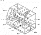
FIG. 2 is a perspective view of a scan and step exposure system with its outer package removed therefrom according to the present invention; -
FIG. 3 is a front view of a scan and step exposure system with its outer package removed therefrom according to the present invention; -
FIG. 4 is a right-side view of a scan and step exposure system with its outer package removed therefrom according to the present invention; -
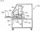
FIG. 5 is a side view of a scan and step exposure system with a chuck tray, a mask holder and an exposure module installed therein according to the present invention; -
FIG. 6 is a perspective view of a scan and step exposure system with a chuck tray installed therein according to the present invention; -
FIG. 7 is a plan view of a scan and step exposure system with a chuck tray drawn therefrom according to the present invention; -
FIG. 8 is a plan view of a scan and step exposure system with a chuck tray being input thereinto according to the present invention; -
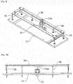
FIG. 9 is a perspective view of a scan and step exposure system with a mask holder installed therein according to the present invention; -
FIG. 10 is a front view of the mask holder according to the present invention; -
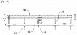
FIG. 11 is a front view of the mask holder descending according to the present invention; -
FIG. 12 is a bottom view of a glass base according to the present invention; -
FIG. 13 is a side-sectional view of the glass base according to the present invention; -
FIG. 14 is a front view of the exposure module installed according to the present invention; -
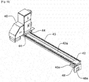
FIG. 15 is a perspective view of the exposure module according to the present invention; and -
FIG. 16 is a front view of the exposure module in operation according to the present invention. - The present invention to achieve the above aspects has the characteristics as follows:
- In accordance with an embodiment of the present invention, there is provided a scan and step exposure system comprising: an exposure body having a front gate selectively being open or closed; a chuck tray having a base plate and a cylinder fix plate spaced from each other at the front and the rear inside the exposure body, and a pair of chuck tray driving cylinder placed across between the base plate and the cylinder fix plate, and a porous chuck placed to be drawn into or out of the exposure body while movable by the chuck tray driving cylinder and sliding along fixed rails fixed at both sides of the base plate; a mask holder being integrally connected with a plurality of guide rods installed on every sides of the base plate to pass through, and selectively moving up and down on the chuck tray by a holder elevating cylinder provided at the middle rear side of the base plate; and an exposure module sliding along LM rails attached to the top of a rail support installed behind the mask holder in the transverse direction, and enabling to move by scan way or move by step feed in the transverse direction by an exposure module transfer motor, and perform the exposure on an exposure subject placed by adsorption on the chuck tray.
- The present invention will now be described more fully hereinafter with reference to the accompanying drawings, in which preferred embodiments of the invention are shown.
- It will be understood that words or terms used in the specification and claims shall not be interpreted as the meaning defined in commonly used dictionaries. It will be further understood that the words or terms should be interpreted as having a meaning that is consistent with their meaning in the context of the relevant art and the technical idea of the invention, based on the principle that an inventor may properly define the meaning of the words or terms to best explain the invention.
As used herein, the singular forms "a", "an" and "the" are intended to include the plural forms as well, unless the context clearly indicates otherwise. - The present invention may be embodied in different forms and should not be construed as limited to the embodiments set forth herein. Rather, these embodiments are provided as teaching examples of the invention. Therefore, it will be understood that the scope of the invention is intended to include various modifications and alternative arrangements within the capabilities of persons skilled in the art using presently known or future technologies and equivalents.
- The scan and step exposure system according to an embodiment of the present invention will be described with reference of drawings. In schematic view, the scan and step exposure system of the present invention includes an
exposure body 10, achuck tray 20, amask holder 30, and anexposure module 40. - Hereinafter, the scan and step exposure system of the present invention will be described in more detail with embodiments.
- A
front gate 11 is installed in theexposure body 10 to enable open and close theexposure body 10 such that thechuck tray 20 is input toward inside or drawn out toward outside, and aglass base 50 is mounted on the top of themask holder 30 installed inside theexposure body 10. - A plurality of
horizontal frames 12 are installed at the middle inside theexposure body 10 with connected to each other, and abase plate 21 and acylinder fix plate 22 are respectively located at the front and the back on thehorizontal frames 12 with distanced from each other, andcylinder brackets base plate 21 and thecylinder fix plate 22 respectively at the middle thereof. A pair of chucktray driving cylinders 24 are provided with held by thecylinder brackets porous chuck 25, which is connected with apiston road 24a of the chucktray driving cylinder 24, moves while sliding by the chucktray driving cylinders 24 along the fixedrails 26 fixed at both sides on thebase plate 21, which is shown as inFIGs 4 and5 , so that theporous chuck 25 is free to move in and out of theexposure body 10. - A plurality of
operation switches 27 are located at the front portion on thechuck tray 20, and behind theoperation switches 27, theporous chuck 25 is mounted in order to fixedly hold anexposure subject 1 by vacuum adsorption for exposure process.Driving rails 28 are integrally attached to the both sides of the bottom of theporous chuck 25 to be connected to the fixedrails 26 so that the chuck tray 20 slides smoothly back and forth. - In the case that the
exposure subject 1 is adsorbed on theporous chuck 25 by applying vacuum adsorption at one time since theporous chuck 25 is shaped as rectangle being long in its length, it is risky that the large-sized exposure subject 1 is not vacuum-adsorbed uniformly in its entire surface, thereby causing theexposure subject 1 to come off from theporous chuck 25 or be distorted in its position. In order to address the problem, theporous chuck 25 is applied into a plurality of division sections along the left and right directions and theexposure subject 1 is put to be mounted on theporous chuck 25 each by each division section with time apart so that theexposure subject 1 is completely adsorbed by vacuum adsorption on theporous chuck 25 throughout its surface, thereby provide the effective results for the exposure in high quality. - The
mask holder 30 is located above thebase plate 21 and is installed to enable move up and down selectively. A plurality ofguide rods 31 are located between themask holder 30 and thebase plate 21 to be distanced from each other and to pass through thebase plate 21. Themask holder 30 in rectangular shape is integrally connected to the top ends of theguide rods 31. Apiston rod 32a of aholder elevating cylinder 32, which is installed at the middle back location on thebase plate 21, is integrally connected to the bottom of themask holder 30 so that themask holder 30 is installed to move up and down selectively by theholder elevating cylinder 32 above thechuck tray 20. - Therefore, the difference in height distanced between the
film mask 2, which is held with safely mounted on themask holder 30, and theexposure subject 1, which is adsorbed on theporous chuck 25, can be controlled to the optimum state easily and effectively, thereby to bring the better results on the exposure process. - The
film mask 2 includes circuits patterns formed thereon. More application of technology can be added without directly mounting thefilm mask 2 on themask holder 30, by applying the technology of adsorbing thefilm mask 2 on the bottom of aglass base 50 safely mounted on themask holder 30 by uniform and close contact way. - As for the constitution by the technology, the
glass base 50 is safely mounted on themask holder 30, avacuum line 51 is provided in dent on the bottom of theglass base 50 around inside the rectangular periphery. On theglass base 50, a plurality ofvacuum ports 52 are provided, going through with thevacuum line 51 and fitted coupled therewith. Thefilm mask 2 having circuit patterns thereon can be closely in flat way contacted to the bottom of theglass base 50 by using vacuum adsorption supplied by the vacuum line 5, thereby greatly enhancing the exposure uniformity. - A plurality of centering
lines 53 are formed out of thevacuum line 51 so as to provide the function to easily meet the center of thefilm mask 2 when fixing thefilm mask 2 to theglass base 50. - A
rail support 42 is installed behind themask holder 30 in the transverse direction. LM rails 43 is attached to the top of therail support 42, and theexposure module 40 is coupled with the LM rails 43 such that theexposure module 40 slidably moves along the LM rails 43. Theexposure module 40 enables to move by step feed in the transverse direction by an exposuremodule transfer motor 48, and perform the exposure on theexposure subject 1 placed by adsorption on thechuck tray 20. - For more detailed description about the constitution of the
exposure module 40, an exposuremodule support frame 41 in rectangular shape is installed in the transverse direction over thehorizontal frame 12, which is placed in the middle of theexposure body 10 at a level with the bottom of the body. A plurality ofsupport legs 41a, which are attached to the bottom of the exposuremodule support frame 41 in the vertical direction, are fixed integrally to thehorizontal frame 12. - The
rail support 42 is installed on the exposuremodule support frame 41 to be safely mounted thereon, and the LM rails 43 are attached on therail support 42 and located respectively at the front and rear of therail support 42 along the longitudinal direction.Carriers 44, which are attached to the front and rear on the bottom of theexposure module 40, are coupled with the LM rails 43 to slidably move along the rails. Aball screw axis 46 is rotationably fitted into theaxis brackets 45a, which are formed with attached to the both sides on the bottom of the exposuremodule support frame 41. At one side of theball screw axis 46, aball nut 47, which is attached to the middle of the bottom of theexposure module 40, is screw-coupled while passing through apath 42a formed in therail support 42. - A
motor fix plate 48a is attached integrally to one side of thesupport leg 41a, and the exposuremodule transfer motor 48 is installed to themotor fix plate 48a. The motor axis of the exposuremodule transfer motor 48 and theball screw axis 46 are connected by amutual timing belt 49 so that the rotation force generated by the operation of the exposuremodule transfer motor 48 is transferred to theball screw axis 46 and while theball screw axis 46 rotates, theball nut 47, which is screw-coupled with theball screw axis 46, is transferred along theball screw axis 46 so that theexposure module 40 moves along the LM rails 43 in the transverse direction continuously at a time like scanning way, or repeatedly step by step like stepping way. Therefore, the exposure process can be possible on the long-lengthen exposure subject 1 regardless of its size and reference so that the work ranges of the exposure system becomes widen, and the availability of the exposure system becomes maximized. - Now then as shown in
FIGs. 3 to 5 , by the structural feature of the present invention as described above, theexposure subject 1 to be exposed is placed on thechuck tray 20 with thechuck tray 20 drawn out of theexposure body 10, and safely placed at its location by adsorption, and thechuck tray 20 having theexposure subject 1 adsorbed thereon is moved in by the operation of the chucktray driving cylinder 24 as shown inFIG. 8 and taken in and placed on the exposure position, that is, under themask holder 30. - Then, with the
glass base 50 turned over, thefilm mask 2 having circuit patterns formed thereon is safely placed on the bottom of theglass base 50 having thevacuum line 51 formed in dent and fixed thereon by using the vacuum adsorption. Theglass base 50 is turned over again with its right top side upward and put to be safely mounted on themask holder 30. While elevating themask holder 30 up and down and controlling the distance from theexposure subject 1 maintained good and optimized, theexposure module 40 is driven to step feed so as to perform the exposure process on the long-length exposure subject 1 by step feed way. - While the invention was described above with reference to the finite embodiments and drawings, the invention is not limited to the embodiments but can be modified and changed in various forms by those skilled in the art without departing from the technical concept of the invention and the equivalents of the appended claims.
| 1: exposure subject | 2: film mask |
| 10: exposure body | 11: front gate |
| 12: horizontal frame | 20: chuck tray |
| 21: base plate | 22: cylinder fix plate |
| 24: chuck tray driving cylinder | 25: porous chuck |
| 26: fixed rail | 28: driving rail |
| 30: mask holder | 31: guide rod |
| 32: holder elevating cylinder | 40: exposure module |
| 41: exposure module support frame | 42: |
| 42a: path | 43: LM rail |
| 44: carrier | 46: ball screw axis |
| 47: ball nut | 48: exposure module transfer motor |
| 49: timing belt | 50: glass base |
| 51: vacuum line | 52: vacuum port |
Claims (5)
- A scan and step exposure system comprising:an exposure body (10) having a front gate (11) selectively being open or closed; a chuck tray (20) having a base plate (21) and a cylinder fix plate (22) spaced from each other at the front and the rear inside the exposure body (10), and a pair of chuck tray driving cylinders (24) placed across between the base plate (21) and the cylinder fix plate (22), and a porous chuck (25) placed to be drawn into or out of the exposure body (10) while movable by the chuck tray driving cylinder (24) and slidable along fixed rails (26) fixed at both sides of the base plate (21);a mask holder (30) being integrally connected with a plurality of guide rods (31) installed on every side of the base plate (21) to pass through the base plate (21), and selectively movable up and down on the chuck tray (20) by a holder elevating cylinder (32) provided at the middle rear side of the base plate (21); andan exposure module (40) slidable along LM rails (43) attached to the top of a rail support (42) installed behind the mask holder (30) in the transverse direction, wherein the exposure system is configured to enable the exposure module to move by scan way or move by step feed in the transverse direction by an exposure module transfer motor (48), and perform the exposure on an exposure subject placed by adsorption on the chuck tray (20).
- The scan and step exposure system according to claim 1, wherein a plurality of operation switches (27) are located at the front portion on the chuck tray (20), and behind the operation switches (27), and driving rails (28) are integrally attached to the both sides of the bottom of the porous chuck (25) to be connected to the fixed rails (26).
- The scan and step exposure system according to claim 1, wherein the rail support (42) is installed to be mounted on an exposure module support frame (41) which is rectangular-shaped and is installed in the transverse direction in the middle of the exposure body (10), and carriers (44), which are attached to the front and rear on the bottom of the exposure module (40), are coupled with the LM rails (43) which are attached respectively at the front and the rear of the rail support (42) along the longitudinal direction, a bail screw axis (46) is rotationably fitted into a pair of axis brackets (45a), which are attached to both sides on the bottom of the exposure module support frame (41), and a ball nut (47), which is,attached to the middle of the bottom of the exposure module (40), is screw-coupled at the ball screw axis (46) through a path (42)a formed in the rail support (42), and the exposure module transfer motor (48) is installed to a support leg (41)a, which is attached to one side of the bottom of the exposure module support frame (41), and the exposure module transfer motor (48) transfers the rotation force to the ball screw axis (46) through a timing belt (49).
- The scan and step exposure system according to claim 1, wherein a glass base (50) is safely mounted on the mask holder (30), and a vacuum line (51) is provided in dent on the bottom of the glass base (50) along the rectangular periphery, and a plurality of vacuum ports (52) are provided on the top of the glass base (50) to be coupled with the vacuum line (51), and the film mask (2) having circuit patterns thereon is fixed to and in close contact with the bottom of the glass base (50).
- The scan and step exposure system according to claim 4, wherein a plurality of centering lines (53) are formed out of the vacuum line (51) to meet and fix the center of the film mask (2) to the glass base (50).
Applications Claiming Priority (2)
| Application Number | Priority Date | Filing Date | Title |
|---|---|---|---|
| KR1020140089707A KR101464706B1 (en) | 2014-07-16 | 2014-07-16 | Scan and step exposure system |
| PCT/KR2015/005048 WO2016010249A1 (en) | 2014-07-16 | 2015-05-20 | Scan and step exposure device |
Publications (3)
| Publication Number | Publication Date |
|---|---|
| EP2993689A1 EP2993689A1 (en) | 2016-03-09 |
| EP2993689A4 EP2993689A4 (en) | 2017-03-01 |
| EP2993689B1 true EP2993689B1 (en) | 2018-01-10 |
Family
ID=52291839
Family Applications (1)
| Application Number | Title | Priority Date | Filing Date |
|---|---|---|---|
| EP15783947.3A Not-in-force EP2993689B1 (en) | 2014-07-16 | 2015-05-20 | Scan and step exposure device |
Country Status (5)
| Country | Link |
|---|---|
| US (1) | US9606455B2 (en) |
| EP (1) | EP2993689B1 (en) |
| KR (1) | KR101464706B1 (en) |
| CN (1) | CN105431925B (en) |
| WO (1) | WO2016010249A1 (en) |
Families Citing this family (3)
| Publication number | Priority date | Publication date | Assignee | Title |
|---|---|---|---|---|
| KR101764836B1 (en) * | 2015-12-14 | 2017-08-14 | 한국기계연구원 | Uv exposure system for biochip fabrication |
| CN108717250B (en) * | 2018-06-05 | 2021-03-23 | 江苏永鼎股份有限公司 | Contact photoetching machine for semiconductor chip production |
| CN110687751B (en) * | 2018-07-05 | 2021-12-28 | 志圣工业股份有限公司 | Exposure equipment comprising glass frame turning frame structure |
Family Cites Families (10)
| Publication number | Priority date | Publication date | Assignee | Title |
|---|---|---|---|---|
| US5617182A (en) * | 1993-11-22 | 1997-04-01 | Nikon Corporation | Scanning exposure method |
| US5721606A (en) * | 1995-09-07 | 1998-02-24 | Jain; Kanti | Large-area, high-throughput, high-resolution, scan-and-repeat, projection patterning system employing sub-full mask |
| KR20030055837A (en) * | 2001-12-27 | 2003-07-04 | 한맥전자 (주) | Exposure machine for lead frame printed circuit board |
| JP4319800B2 (en) * | 2002-01-24 | 2009-08-26 | 大日本印刷株式会社 | Large size photomask laser exposure apparatus and laser drawing method |
| US7304720B2 (en) * | 2002-02-22 | 2007-12-04 | Asml Holding N.V. | System for using a two part cover for protecting a reticle |
| JP5190860B2 (en) * | 2007-01-22 | 2013-04-24 | 学校法人東京電機大学 | Projection exposure apparatus and projection exposure method |
| CN102449553B (en) * | 2010-06-17 | 2014-07-09 | 恩斯克科技有限公司 | Exposure apparatus |
| KR101219323B1 (en) * | 2010-09-16 | 2013-01-18 | 엘지이노텍 주식회사 | Photolithography apparatus |
| CN202041765U (en) * | 2011-05-10 | 2011-11-16 | 志圣科技(广州)有限公司 | Light source device and exposure machine with same |
| KR101379379B1 (en) | 2012-11-09 | 2014-03-28 | 나노전광 주식회사 | Wafer chuck balancing apparatus for stepper |
-
2014
- 2014-07-16 KR KR1020140089707A patent/KR101464706B1/en active Active
-
2015
- 2015-05-20 US US14/888,233 patent/US9606455B2/en not_active Expired - Fee Related
- 2015-05-20 WO PCT/KR2015/005048 patent/WO2016010249A1/en not_active Ceased
- 2015-05-20 CN CN201580000661.7A patent/CN105431925B/en not_active Expired - Fee Related
- 2015-05-20 EP EP15783947.3A patent/EP2993689B1/en not_active Not-in-force
Non-Patent Citations (1)
| Title |
|---|
| None * |
Also Published As
| Publication number | Publication date |
|---|---|
| KR101464706B1 (en) | 2014-11-28 |
| EP2993689A4 (en) | 2017-03-01 |
| US9606455B2 (en) | 2017-03-28 |
| CN105431925A (en) | 2016-03-23 |
| EP2993689A1 (en) | 2016-03-09 |
| US20160161853A1 (en) | 2016-06-09 |
| WO2016010249A1 (en) | 2016-01-21 |
| CN105431925B (en) | 2018-01-16 |
Similar Documents
| Publication | Publication Date | Title |
|---|---|---|
| US8289496B2 (en) | System and method for treating substrate | |
| US9463938B2 (en) | Substrate heat treatment device | |
| KR101256791B1 (en) | Exposure apparatus | |
| US9606455B2 (en) | Scan and step exposure system | |
| US10289005B2 (en) | Unit for supplying liquid, apparatus for treating a substrate, and method for treating a substrate | |
| KR20160108653A (en) | Method and Apparatus for treating substrate | |
| KR20190011854A (en) | Method and Apparatus for treating substrate | |
| JP2009258195A (en) | Proximity exposure device, substrate moving method for proximity exposure device, and method of manufacturing display panel | |
| KR20150078629A (en) | Apparatus for treating substrate | |
| KR101769440B1 (en) | Method for treating substrate | |
| KR102315660B1 (en) | Apparatus and Method for treating substrate | |
| KR20140101946A (en) | lift pin assembly | |
| KR102000023B1 (en) | Substrate treating apparatus | |
| KR102223764B1 (en) | Apparatus and Method for treating substrate | |
| KR101681185B1 (en) | Interface module, apparatus and method for treating substrate comprising the same | |
| KR20180058390A (en) | Substrate treating apparatus and substrate treating method | |
| JP5047040B2 (en) | Proximity exposure apparatus, substrate moving method of proximity exposure apparatus, and display panel substrate manufacturing method | |
| KR102156897B1 (en) | Apparatus and Method for treating substrate | |
| KR101842121B1 (en) | Apparatus for treating substrate and method for controlling driving speed thereof | |
| KR20160135905A (en) | method and Apparatus for treating substrate | |
| KR102296277B1 (en) | Substrate treating apparatus | |
| KR102223762B1 (en) | Apparatus and Method for treating substrate | |
| KR102231773B1 (en) | Method and Apparatus for treating substrate | |
| JP2013070038A (en) | Lithographic apparatus and substrate handling method | |
| KR20160078581A (en) | Method for supplying chemical and Apparatus for treating substrate |
Legal Events
| Date | Code | Title | Description |
|---|---|---|---|
| PUAI | Public reference made under article 153(3) epc to a published international application that has entered the european phase |
Free format text: ORIGINAL CODE: 0009012 |
|
| 17P | Request for examination filed |
Effective date: 20151030 |
|
| AK | Designated contracting states |
Kind code of ref document: A1 Designated state(s): AL AT BE BG CH CY CZ DE DK EE ES FI FR GB GR HR HU IE IS IT LI LT LU LV MC MK MT NL NO PL PT RO RS SE SI SK SM TR |
|
| AX | Request for extension of the european patent |
Extension state: BA ME |
|
| REG | Reference to a national code |
Ref country code: DE Ref legal event code: R079 Ref document number: 602015007497 Country of ref document: DE Free format text: PREVIOUS MAIN CLASS: H01L0021027000 Ipc: G03F0007200000 |
|
| A4 | Supplementary search report drawn up and despatched |
Effective date: 20170126 |
|
| RIC1 | Information provided on ipc code assigned before grant |
Ipc: H01L 21/027 20060101ALI20170120BHEP Ipc: G03F 7/20 20060101AFI20170120BHEP |
|
| DAV | Request for validation of the european patent (deleted) | ||
| DAX | Request for extension of the european patent (deleted) | ||
| GRAP | Despatch of communication of intention to grant a patent |
Free format text: ORIGINAL CODE: EPIDOSNIGR1 |
|
| INTG | Intention to grant announced |
Effective date: 20170731 |
|
| GRAS | Grant fee paid |
Free format text: ORIGINAL CODE: EPIDOSNIGR3 |
|
| GRAA | (expected) grant |
Free format text: ORIGINAL CODE: 0009210 |
|
| AK | Designated contracting states |
Kind code of ref document: B1 Designated state(s): AL AT BE BG CH CY CZ DE DK EE ES FI FR GB GR HR HU IE IS IT LI LT LU LV MC MK MT NL NO PL PT RO RS SE SI SK SM TR |
|
| REG | Reference to a national code |
Ref country code: CH Ref legal event code: EP Ref country code: AT Ref legal event code: REF Ref document number: 963032 Country of ref document: AT Kind code of ref document: T Effective date: 20180115 |
|
| REG | Reference to a national code |
Ref country code: IE Ref legal event code: FG4D |
|
| REG | Reference to a national code |
Ref country code: DE Ref legal event code: R096 Ref document number: 602015007497 Country of ref document: DE |
|
| REG | Reference to a national code |
Ref country code: NL Ref legal event code: MP Effective date: 20180110 |
|
| REG | Reference to a national code |
Ref country code: FR Ref legal event code: PLFP Year of fee payment: 4 |
|
| REG | Reference to a national code |
Ref country code: AT Ref legal event code: MK05 Ref document number: 963032 Country of ref document: AT Kind code of ref document: T Effective date: 20180110 |
|
| PG25 | Lapsed in a contracting state [announced via postgrant information from national office to epo] |
Ref country code: NL Free format text: LAPSE BECAUSE OF FAILURE TO SUBMIT A TRANSLATION OF THE DESCRIPTION OR TO PAY THE FEE WITHIN THE PRESCRIBED TIME-LIMIT Effective date: 20180110 |
|
| PG25 | Lapsed in a contracting state [announced via postgrant information from national office to epo] |
Ref country code: ES Free format text: LAPSE BECAUSE OF FAILURE TO SUBMIT A TRANSLATION OF THE DESCRIPTION OR TO PAY THE FEE WITHIN THE PRESCRIBED TIME-LIMIT Effective date: 20180110 Ref country code: LT Free format text: LAPSE BECAUSE OF FAILURE TO SUBMIT A TRANSLATION OF THE DESCRIPTION OR TO PAY THE FEE WITHIN THE PRESCRIBED TIME-LIMIT Effective date: 20180110 Ref country code: NO Free format text: LAPSE BECAUSE OF FAILURE TO SUBMIT A TRANSLATION OF THE DESCRIPTION OR TO PAY THE FEE WITHIN THE PRESCRIBED TIME-LIMIT Effective date: 20180410 Ref country code: HR Free format text: LAPSE BECAUSE OF FAILURE TO SUBMIT A TRANSLATION OF THE DESCRIPTION OR TO PAY THE FEE WITHIN THE PRESCRIBED TIME-LIMIT Effective date: 20180110 Ref country code: FI Free format text: LAPSE BECAUSE OF FAILURE TO SUBMIT A TRANSLATION OF THE DESCRIPTION OR TO PAY THE FEE WITHIN THE PRESCRIBED TIME-LIMIT Effective date: 20180110 Ref country code: CY Free format text: LAPSE BECAUSE OF FAILURE TO SUBMIT A TRANSLATION OF THE DESCRIPTION OR TO PAY THE FEE WITHIN THE PRESCRIBED TIME-LIMIT Effective date: 20180110 |
|
| PG25 | Lapsed in a contracting state [announced via postgrant information from national office to epo] |
Ref country code: LV Free format text: LAPSE BECAUSE OF FAILURE TO SUBMIT A TRANSLATION OF THE DESCRIPTION OR TO PAY THE FEE WITHIN THE PRESCRIBED TIME-LIMIT Effective date: 20180110 Ref country code: SE Free format text: LAPSE BECAUSE OF FAILURE TO SUBMIT A TRANSLATION OF THE DESCRIPTION OR TO PAY THE FEE WITHIN THE PRESCRIBED TIME-LIMIT Effective date: 20180110 Ref country code: PL Free format text: LAPSE BECAUSE OF FAILURE TO SUBMIT A TRANSLATION OF THE DESCRIPTION OR TO PAY THE FEE WITHIN THE PRESCRIBED TIME-LIMIT Effective date: 20180110 Ref country code: IS Free format text: LAPSE BECAUSE OF FAILURE TO SUBMIT A TRANSLATION OF THE DESCRIPTION OR TO PAY THE FEE WITHIN THE PRESCRIBED TIME-LIMIT Effective date: 20180510 Ref country code: GR Free format text: LAPSE BECAUSE OF FAILURE TO SUBMIT A TRANSLATION OF THE DESCRIPTION OR TO PAY THE FEE WITHIN THE PRESCRIBED TIME-LIMIT Effective date: 20180411 Ref country code: BG Free format text: LAPSE BECAUSE OF FAILURE TO SUBMIT A TRANSLATION OF THE DESCRIPTION OR TO PAY THE FEE WITHIN THE PRESCRIBED TIME-LIMIT Effective date: 20180410 Ref country code: RS Free format text: LAPSE BECAUSE OF FAILURE TO SUBMIT A TRANSLATION OF THE DESCRIPTION OR TO PAY THE FEE WITHIN THE PRESCRIBED TIME-LIMIT Effective date: 20180110 Ref country code: AT Free format text: LAPSE BECAUSE OF FAILURE TO SUBMIT A TRANSLATION OF THE DESCRIPTION OR TO PAY THE FEE WITHIN THE PRESCRIBED TIME-LIMIT Effective date: 20180110 |
|
| REG | Reference to a national code |
Ref country code: DE Ref legal event code: R097 Ref document number: 602015007497 Country of ref document: DE |
|
| PG25 | Lapsed in a contracting state [announced via postgrant information from national office to epo] |
Ref country code: IT Free format text: LAPSE BECAUSE OF FAILURE TO SUBMIT A TRANSLATION OF THE DESCRIPTION OR TO PAY THE FEE WITHIN THE PRESCRIBED TIME-LIMIT Effective date: 20180110 Ref country code: AL Free format text: LAPSE BECAUSE OF FAILURE TO SUBMIT A TRANSLATION OF THE DESCRIPTION OR TO PAY THE FEE WITHIN THE PRESCRIBED TIME-LIMIT Effective date: 20180110 Ref country code: EE Free format text: LAPSE BECAUSE OF FAILURE TO SUBMIT A TRANSLATION OF THE DESCRIPTION OR TO PAY THE FEE WITHIN THE PRESCRIBED TIME-LIMIT Effective date: 20180110 Ref country code: RO Free format text: LAPSE BECAUSE OF FAILURE TO SUBMIT A TRANSLATION OF THE DESCRIPTION OR TO PAY THE FEE WITHIN THE PRESCRIBED TIME-LIMIT Effective date: 20180110 |
|
| PLBE | No opposition filed within time limit |
Free format text: ORIGINAL CODE: 0009261 |
|
| STAA | Information on the status of an ep patent application or granted ep patent |
Free format text: STATUS: NO OPPOSITION FILED WITHIN TIME LIMIT |
|
| PG25 | Lapsed in a contracting state [announced via postgrant information from national office to epo] |
Ref country code: SM Free format text: LAPSE BECAUSE OF FAILURE TO SUBMIT A TRANSLATION OF THE DESCRIPTION OR TO PAY THE FEE WITHIN THE PRESCRIBED TIME-LIMIT Effective date: 20180110 Ref country code: CZ Free format text: LAPSE BECAUSE OF FAILURE TO SUBMIT A TRANSLATION OF THE DESCRIPTION OR TO PAY THE FEE WITHIN THE PRESCRIBED TIME-LIMIT Effective date: 20180110 Ref country code: SK Free format text: LAPSE BECAUSE OF FAILURE TO SUBMIT A TRANSLATION OF THE DESCRIPTION OR TO PAY THE FEE WITHIN THE PRESCRIBED TIME-LIMIT Effective date: 20180110 Ref country code: DK Free format text: LAPSE BECAUSE OF FAILURE TO SUBMIT A TRANSLATION OF THE DESCRIPTION OR TO PAY THE FEE WITHIN THE PRESCRIBED TIME-LIMIT Effective date: 20180110 |
|
| REG | Reference to a national code |
Ref country code: CH Ref legal event code: PL |
|
| 26N | No opposition filed |
Effective date: 20181011 |
|
| REG | Reference to a national code |
Ref country code: BE Ref legal event code: MM Effective date: 20180531 |
|
| PG25 | Lapsed in a contracting state [announced via postgrant information from national office to epo] |
Ref country code: MC Free format text: LAPSE BECAUSE OF FAILURE TO SUBMIT A TRANSLATION OF THE DESCRIPTION OR TO PAY THE FEE WITHIN THE PRESCRIBED TIME-LIMIT Effective date: 20180110 |
|
| REG | Reference to a national code |
Ref country code: IE Ref legal event code: MM4A |
|
| PG25 | Lapsed in a contracting state [announced via postgrant information from national office to epo] |
Ref country code: LI Free format text: LAPSE BECAUSE OF NON-PAYMENT OF DUE FEES Effective date: 20180531 Ref country code: SI Free format text: LAPSE BECAUSE OF FAILURE TO SUBMIT A TRANSLATION OF THE DESCRIPTION OR TO PAY THE FEE WITHIN THE PRESCRIBED TIME-LIMIT Effective date: 20180110 Ref country code: CH Free format text: LAPSE BECAUSE OF NON-PAYMENT OF DUE FEES Effective date: 20180531 |
|
| PG25 | Lapsed in a contracting state [announced via postgrant information from national office to epo] |
Ref country code: LU Free format text: LAPSE BECAUSE OF NON-PAYMENT OF DUE FEES Effective date: 20180520 |
|
| PG25 | Lapsed in a contracting state [announced via postgrant information from national office to epo] |
Ref country code: IE Free format text: LAPSE BECAUSE OF NON-PAYMENT OF DUE FEES Effective date: 20180520 |
|
| PG25 | Lapsed in a contracting state [announced via postgrant information from national office to epo] |
Ref country code: BE Free format text: LAPSE BECAUSE OF NON-PAYMENT OF DUE FEES Effective date: 20180531 |
|
| PG25 | Lapsed in a contracting state [announced via postgrant information from national office to epo] |
Ref country code: MT Free format text: LAPSE BECAUSE OF NON-PAYMENT OF DUE FEES Effective date: 20180520 |
|
| PG25 | Lapsed in a contracting state [announced via postgrant information from national office to epo] |
Ref country code: TR Free format text: LAPSE BECAUSE OF FAILURE TO SUBMIT A TRANSLATION OF THE DESCRIPTION OR TO PAY THE FEE WITHIN THE PRESCRIBED TIME-LIMIT Effective date: 20180110 |
|
| PG25 | Lapsed in a contracting state [announced via postgrant information from national office to epo] |
Ref country code: PT Free format text: LAPSE BECAUSE OF FAILURE TO SUBMIT A TRANSLATION OF THE DESCRIPTION OR TO PAY THE FEE WITHIN THE PRESCRIBED TIME-LIMIT Effective date: 20180110 |
|
| PG25 | Lapsed in a contracting state [announced via postgrant information from national office to epo] |
Ref country code: HU Free format text: LAPSE BECAUSE OF FAILURE TO SUBMIT A TRANSLATION OF THE DESCRIPTION OR TO PAY THE FEE WITHIN THE PRESCRIBED TIME-LIMIT; INVALID AB INITIO Effective date: 20150520 Ref country code: MK Free format text: LAPSE BECAUSE OF NON-PAYMENT OF DUE FEES Effective date: 20180110 |
|
| PGFP | Annual fee paid to national office [announced via postgrant information from national office to epo] |
Ref country code: FR Payment date: 20230531 Year of fee payment: 9 Ref country code: DE Payment date: 20230526 Year of fee payment: 9 |
|
| PGFP | Annual fee paid to national office [announced via postgrant information from national office to epo] |
Ref country code: GB Payment date: 20230531 Year of fee payment: 9 |
|
| REG | Reference to a national code |
Ref country code: DE Ref legal event code: R119 Ref document number: 602015007497 Country of ref document: DE |
|
| GBPC | Gb: european patent ceased through non-payment of renewal fee |
Effective date: 20240520 |
|
| PG25 | Lapsed in a contracting state [announced via postgrant information from national office to epo] |
Ref country code: DE Free format text: LAPSE BECAUSE OF NON-PAYMENT OF DUE FEES Effective date: 20241203 |
|
| PG25 | Lapsed in a contracting state [announced via postgrant information from national office to epo] |
Ref country code: FR Free format text: LAPSE BECAUSE OF NON-PAYMENT OF DUE FEES Effective date: 20240531 |
|
| PG25 | Lapsed in a contracting state [announced via postgrant information from national office to epo] |
Ref country code: GB Free format text: LAPSE BECAUSE OF NON-PAYMENT OF DUE FEES Effective date: 20240520 |