EP2987392B1 - Elektronisches gerät - Google Patents
Elektronisches gerät Download PDFInfo
- Publication number
- EP2987392B1 EP2987392B1 EP14718562.3A EP14718562A EP2987392B1 EP 2987392 B1 EP2987392 B1 EP 2987392B1 EP 14718562 A EP14718562 A EP 14718562A EP 2987392 B1 EP2987392 B1 EP 2987392B1
- Authority
- EP
- European Patent Office
- Prior art keywords
- screw
- electronic device
- circuit board
- printed circuit
- contact element
- Prior art date
- Legal status (The legal status is an assumption and is not a legal conclusion. Google has not performed a legal analysis and makes no representation as to the accuracy of the status listed.)
- Not-in-force
Links
- 230000008859 change Effects 0.000 claims description 7
- 238000000926 separation method Methods 0.000 claims description 3
- 238000001746 injection moulding Methods 0.000 claims description 2
- 239000002184 metal Substances 0.000 claims description 2
- 239000002991 molded plastic Substances 0.000 claims 1
- 230000006872 improvement Effects 0.000 description 2
- 238000002347 injection Methods 0.000 description 2
- 239000007924 injection Substances 0.000 description 2
- 229910000639 Spring steel Inorganic materials 0.000 description 1
- 239000000853 adhesive Substances 0.000 description 1
- 230000001070 adhesive effect Effects 0.000 description 1
- 230000000903 blocking effect Effects 0.000 description 1
- 239000004020 conductor Substances 0.000 description 1
- 238000012217 deletion Methods 0.000 description 1
- 230000037430 deletion Effects 0.000 description 1
- 230000001419 dependent effect Effects 0.000 description 1
- 238000001514 detection method Methods 0.000 description 1
- 230000002349 favourable effect Effects 0.000 description 1
- 238000012423 maintenance Methods 0.000 description 1
- 238000004519 manufacturing process Methods 0.000 description 1
- 230000009467 reduction Effects 0.000 description 1
- 230000008439 repair process Effects 0.000 description 1
- 230000007704 transition Effects 0.000 description 1
Images
Classifications
-
- H—ELECTRICITY
- H05—ELECTRIC TECHNIQUES NOT OTHERWISE PROVIDED FOR
- H05K—PRINTED CIRCUITS; CASINGS OR CONSTRUCTIONAL DETAILS OF ELECTRIC APPARATUS; MANUFACTURE OF ASSEMBLAGES OF ELECTRICAL COMPONENTS
- H05K5/00—Casings, cabinets or drawers for electric apparatus
- H05K5/02—Details
- H05K5/0208—Interlock mechanisms; Means for avoiding unauthorised use or function, e.g. tamperproof
-
- H—ELECTRICITY
- H01—ELECTRIC ELEMENTS
- H01R—ELECTRICALLY-CONDUCTIVE CONNECTIONS; STRUCTURAL ASSOCIATIONS OF A PLURALITY OF MUTUALLY-INSULATED ELECTRICAL CONNECTING ELEMENTS; COUPLING DEVICES; CURRENT COLLECTORS
- H01R12/00—Structural associations of a plurality of mutually-insulated electrical connecting elements, specially adapted for printed circuits, e.g. printed circuit boards [PCB], flat or ribbon cables, or like generally planar structures, e.g. terminal strips, terminal blocks; Coupling devices specially adapted for printed circuits, flat or ribbon cables, or like generally planar structures; Terminals specially adapted for contact with, or insertion into, printed circuits, flat or ribbon cables, or like generally planar structures
- H01R12/50—Fixed connections
- H01R12/51—Fixed connections for rigid printed circuits or like structures
- H01R12/52—Fixed connections for rigid printed circuits or like structures connecting to other rigid printed circuits or like structures
-
- G—PHYSICS
- G01—MEASURING; TESTING
- G01R—MEASURING ELECTRIC VARIABLES; MEASURING MAGNETIC VARIABLES
- G01R31/00—Arrangements for testing electric properties; Arrangements for locating electric faults; Arrangements for electrical testing characterised by what is being tested not provided for elsewhere
- G01R31/28—Testing of electronic circuits, e.g. by signal tracer
- G01R31/2801—Testing of printed circuits, backplanes, motherboards, hybrid circuits or carriers for multichip packages [MCP]
- G01R31/281—Specific types of tests or tests for a specific type of fault, e.g. thermal mapping, shorts testing
- G01R31/2812—Checking for open circuits or shorts, e.g. solder bridges; Testing conductivity, resistivity or impedance
-
- H—ELECTRICITY
- H01—ELECTRIC ELEMENTS
- H01R—ELECTRICALLY-CONDUCTIVE CONNECTIONS; STRUCTURAL ASSOCIATIONS OF A PLURALITY OF MUTUALLY-INSULATED ELECTRICAL CONNECTING ELEMENTS; COUPLING DEVICES; CURRENT COLLECTORS
- H01R4/00—Electrically-conductive connections between two or more conductive members in direct contact, i.e. touching one another; Means for effecting or maintaining such contact; Electrically-conductive connections having two or more spaced connecting locations for conductors and using contact members penetrating insulation
- H01R4/28—Clamped connections, spring connections
- H01R4/30—Clamped connections, spring connections utilising a screw or nut clamping member
- H01R4/304—Clamped connections, spring connections utilising a screw or nut clamping member having means for improving contact
-
- H—ELECTRICITY
- H01—ELECTRIC ELEMENTS
- H01R—ELECTRICALLY-CONDUCTIVE CONNECTIONS; STRUCTURAL ASSOCIATIONS OF A PLURALITY OF MUTUALLY-INSULATED ELECTRICAL CONNECTING ELEMENTS; COUPLING DEVICES; CURRENT COLLECTORS
- H01R4/00—Electrically-conductive connections between two or more conductive members in direct contact, i.e. touching one another; Means for effecting or maintaining such contact; Electrically-conductive connections having two or more spaced connecting locations for conductors and using contact members penetrating insulation
- H01R4/28—Clamped connections, spring connections
- H01R4/30—Clamped connections, spring connections utilising a screw or nut clamping member
- H01R4/305—Clamped connections, spring connections utilising a screw or nut clamping member having means for facilitating engagement of conductive member or for holding it in position
-
- H—ELECTRICITY
- H05—ELECTRIC TECHNIQUES NOT OTHERWISE PROVIDED FOR
- H05K—PRINTED CIRCUITS; CASINGS OR CONSTRUCTIONAL DETAILS OF ELECTRIC APPARATUS; MANUFACTURE OF ASSEMBLAGES OF ELECTRICAL COMPONENTS
- H05K1/00—Printed circuits
- H05K1/02—Details
- H05K1/14—Structural association of two or more printed circuits
- H05K1/142—Arrangements of planar printed circuit boards in the same plane, e.g. auxiliary printed circuit insert mounted in a main printed circuit
-
- G—PHYSICS
- G01—MEASURING; TESTING
- G01R—MEASURING ELECTRIC VARIABLES; MEASURING MAGNETIC VARIABLES
- G01R31/00—Arrangements for testing electric properties; Arrangements for locating electric faults; Arrangements for electrical testing characterised by what is being tested not provided for elsewhere
- G01R31/50—Testing of electric apparatus, lines, cables or components for short-circuits, continuity, leakage current or incorrect line connections
- G01R31/66—Testing of connections, e.g. of plugs or non-disconnectable joints
- G01R31/70—Testing of connections between components and printed circuit boards
-
- H—ELECTRICITY
- H05—ELECTRIC TECHNIQUES NOT OTHERWISE PROVIDED FOR
- H05K—PRINTED CIRCUITS; CASINGS OR CONSTRUCTIONAL DETAILS OF ELECTRIC APPARATUS; MANUFACTURE OF ASSEMBLAGES OF ELECTRICAL COMPONENTS
- H05K2201/00—Indexing scheme relating to printed circuits covered by H05K1/00
- H05K2201/03—Conductive materials
- H05K2201/0332—Structure of the conductor
- H05K2201/0364—Conductor shape
- H05K2201/0376—Flush conductors, i.e. flush with the surface of the printed circuit
-
- H—ELECTRICITY
- H05—ELECTRIC TECHNIQUES NOT OTHERWISE PROVIDED FOR
- H05K—PRINTED CIRCUITS; CASINGS OR CONSTRUCTIONAL DETAILS OF ELECTRIC APPARATUS; MANUFACTURE OF ASSEMBLAGES OF ELECTRICAL COMPONENTS
- H05K2201/00—Indexing scheme relating to printed circuits covered by H05K1/00
- H05K2201/09—Shape and layout
- H05K2201/09009—Substrate related
- H05K2201/09063—Holes or slots in insulating substrate not used for electrical connections
-
- H—ELECTRICITY
- H05—ELECTRIC TECHNIQUES NOT OTHERWISE PROVIDED FOR
- H05K—PRINTED CIRCUITS; CASINGS OR CONSTRUCTIONAL DETAILS OF ELECTRIC APPARATUS; MANUFACTURE OF ASSEMBLAGES OF ELECTRICAL COMPONENTS
- H05K2201/00—Indexing scheme relating to printed circuits covered by H05K1/00
- H05K2201/10—Details of components or other objects attached to or integrated in a printed circuit board
- H05K2201/10227—Other objects, e.g. metallic pieces
- H05K2201/10409—Screws
-
- H—ELECTRICITY
- H05—ELECTRIC TECHNIQUES NOT OTHERWISE PROVIDED FOR
- H05K—PRINTED CIRCUITS; CASINGS OR CONSTRUCTIONAL DETAILS OF ELECTRIC APPARATUS; MANUFACTURE OF ASSEMBLAGES OF ELECTRICAL COMPONENTS
- H05K2201/00—Indexing scheme relating to printed circuits covered by H05K1/00
- H05K2201/10—Details of components or other objects attached to or integrated in a printed circuit board
- H05K2201/10431—Details of mounted components
- H05K2201/10598—Means for fastening a component, a casing or a heat sink whereby a pressure is exerted on the component towards the PCB
-
- H—ELECTRICITY
- H05—ELECTRIC TECHNIQUES NOT OTHERWISE PROVIDED FOR
- H05K—PRINTED CIRCUITS; CASINGS OR CONSTRUCTIONAL DETAILS OF ELECTRIC APPARATUS; MANUFACTURE OF ASSEMBLAGES OF ELECTRICAL COMPONENTS
- H05K9/00—Screening of apparatus or components against electric or magnetic fields
- H05K9/0007—Casings
- H05K9/002—Casings with localised screening
- H05K9/0039—Galvanic coupling of ground layer on printed circuit board [PCB] to conductive casing
Definitions
- the invention relates to an electronic device with special safety requirements, which comprises a printed circuit board, wherein the circuit board is enclosed by a housing comprising two housing parts connected by a screw, wherein a separation of the housing parts inevitably causes a change in state of the electronic device, wherein a first electrically conductive contact element is contacted with a first circuit board contact and rests against the screw in the screwed state and wherein a second electrically conductive contact element is contacted with a second circuit board contact and rests against the screw in the screwed state, so when screwed screw between the two circuit board contacts an electrical connection ,
- Multi-part housings are usually screwed in order to open the case during maintenance or repair operations can.
- the housing is opened by a device user. If this happens, the separation of the housing parts inevitably causes a state change of the electronic device.
- an electronic switch is arranged on a printed circuit board, which is in contact with a housing part. A release of the housing part actuates the switch, whereby the device changes its state. This change ranges, for example, from an electronic logging of the device manipulation to a permanent functional restriction of the device.
- Tamper protection with several contacted housing closure screws is from the US 2002/014962 A1 known.
- the screws are electrically connected via contact elements. If a screw is unscrewed, the connection is released, indicating a manipulation.
- a tamper-proof, multi-layer printed circuit board assembly is from the EP 2 330 528 A2 known.
- a first layer forms a printed circuit board whose upper side is equipped with a cryptographic processor.
- a space applied flatly to the printed circuit board has a recess at the position of the processor. Covered is the distance position by means of another layer, so that the processor is enclosed on all sides.
- the EP 0 540 376 A1 shows an arrangement with a circuit board, which is held by a screw between two housing parts.
- the circuit board Around a recess for screw passage, the circuit board has two concentrically arranged contact surfaces, which are electrically connected in the mounted state by means of a washer. Removal of the screw and, subsequently, the washer breaks the connection, thereby detecting a tampering attempt on the assembly.
- An electronic device with special security requirements is designed, for example, as on-board information system, like the EP 2 466 682 A1 disclosed.
- the invention has for its object to provide an improvement over the prior art for an electronic device of the type mentioned.
- a first electrically conductive contact element is contacted with a first circuit board contact and is applied to the screw in the screwed state.
- a second electrically conductive contact element is contacted with a second circuit board contact and abuts the screw in the screwed state, so that when screwed screw between the two PCB contacts, there is an electrical connection.
- About the electrically conductive screw thus takes place when the housing is closed safe and durable electrical connection of the two PCB contacts. Once the screw is unscrewed, this electrical connection inevitably detaches, causing the device to change state. For example, registers an electronic circuit interruption of the two PCB contacts.
- a separate switch, which is coupled to a housing part is eliminated. The blocking of a switch, for example by injecting an adhesive, is thus excluded.
- the invention enables a simple and fault-tolerant design of a protected device housing.
- the contact elements are in the manner of the screw, that the electrical connection of the two PCB contacts only when completely screwed Screw is given. This prevents that only a slight opening of the device housing remains without consequences. As soon as the housing parts are loosened by means of the screw, the electrical connection between the printed circuit board contacts inevitably comes loose with the intended consequence of a device state change.
- the electronic device comprises a memory element and a microprocessor, wherein the memory element is at least partially deleted as soon as the electrical connection between the PCB contacts is interrupted.
- the memory element is at least partially deleted as soon as the electrical connection between the PCB contacts is interrupted.
- a further embodiment provides that the electronic device is an on-board unit arranged in a vehicle.
- Such devices are used for example for toll collection and must therefore be protected against unauthorized access. Since toll collection devices are manufactured in large numbers, here the simple case protection structure according to the invention is particularly advantageous because many components for detecting device manipulation (e.g., switches) are saved.
- At least one contact element is designed as a metal spring. Then, the contact element bears against the screw with a spring force, whereby a permanent, vibration-resistant electrical connection is provided.
- At least one housing part is made as a plastic injection molded product and that at least one of the contact elements is molded.
- each housing part has extensions which are designed as holders for the printed circuit board.
- the circuit board is fixed during assembly of the housing by means of these brackets, so that no further PCB mounting is required.
- Such extensions may for example be fastening domes around the mounting holes provided for the attachment of the screw.
- first contact element between the circuit board and the first housing part is clamped.
- second contact element which is conveniently clamped between the printed circuit board and the second housing part. In this way, an electrical connection between the contact elements and the PCB contacts in the course of the housing assembly.
- Another favorable expression provides that the first contact element between the first housing part and the head of the screw is clamped. Furthermore, it is advantageous if the second contact element protrudes into a mounting hole of the second housing part, so that the end of the second contact element bears against the shaft of the screw when the screw is screwed in. Once the screw is screwed into the mounting hole and the screw head rests against the housing, the electrical connection between the PCB contacts. Conversely, this electrical connection dissolves as soon as the screw head is only slightly unscrewed. Such an expression is also insensitive to Genzoverwindungen because the electrical contacts are located directly at the screw.
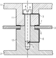
- the Fig. Shows a section of an assembled housing.
- a first housing part 1 is connected by means of a screw 4 with a second housing part 2.
- the housing parts 1, 2 are injection molded from plastic. They are made thin-walled, with fastening domes 11, 12 being provided around the fastening holes.
- the attachment hole of the first housing part 1 has a cylindrical countersink. In this reduction, the head of the screw 4 is sunk in the assembled state.
- the thread in the mounting hole of the second Housing part 2 is advantageously formed as a result of the screwing of the screw. 4
- the attachment domes 11, 12 of the two housing parts 1, 2 form a holder for a printed circuit board 3.
- the fixing dome 12 of the second housing part 2 is offset at its end, wherein the shoulder forms a clearance fit with an opening in the printed circuit board 3.
- the circuit board 3 is fixed by an end-face support of the mounting dome 11 of the first housing part 1. An additional fixation of the circuit board 3 is not required.
- the bearing surfaces of the printed circuit board 3 on the two Befest Trentsdomen 11, 12 are used to produce an electrical connection to two contact elements 5, 6 in the assembled state.
- the circuit board 3 has for this purpose around the breakthrough on each side of a circuit board contact 7, 8, which are connected via interconnects with an electronic circuit.
- Each of these printed circuit board contacts 7, 8 is contacted with a correspondingly shaped contact element 5, 6.
- the contact elements 5, 6 are made of spring steel and injected with the respective housing part 1, 2.
- the contact elements 5, 6 are inserted after the injection molding of the housing parts 1, 2 in recesses provided for this purpose.
- the first contact element 5 connects the first circuit board contact 7 with a screw contact surface 9, which is present for example in the form of the annular head end face of the screw at the transition to the screw shaft.
- the end of the contact element 5 is like a washer below the screw head, without the inner edge of this disc touches the screw shaft.
- the end 10 of the second contact element 6 is guided in the mounting hole in such a way that the fully screwed screw 4 with its shaft inevitably presses against this end 10 of the second contact element 6.
- the two PCB contacts 7, 8 are then electrically connected to each other via the completely screwed screw 4.
- the PCB contacts 7, 8 are connected to an electronic circuit, not shown.
- the electronic circuit with the microprocessor is arranged to detect an interruption of the electrical connection of the two printed circuit board contacts 7, 8 and to bring about a change of state of the electronic device.
Landscapes
- Engineering & Computer Science (AREA)
- Microelectronics & Electronic Packaging (AREA)
- Computer Security & Cryptography (AREA)
- Computer Hardware Design (AREA)
- General Engineering & Computer Science (AREA)
- Physics & Mathematics (AREA)
- General Physics & Mathematics (AREA)
- Mounting Of Printed Circuit Boards And The Like (AREA)
- Casings For Electric Apparatus (AREA)
- Structures For Mounting Electric Components On Printed Circuit Boards (AREA)
- Storage Device Security (AREA)
Description
- Die Erfindung betrifft ein elektronisches Gerät mit besonderen Sicherheitsanforderungen, welches eine Leiterplatte umfasst, wobei die Leiterplatte umschlossen ist von einem Gehäuse, das zwei mittels einer Schraube verbundene Gehäuseteile umfasst, wobei eine Trennung der Gehäuseteile zwangsläufig eine Zustandsänderung des elektronischen Gerätes bewirkt, wobei ein erstes elektrisch leitendes Kontaktelement mit einem ersten Leiterplattenkontakt kontaktiert ist und an der Schraube im eingeschraubten Zustand anliegt und wobei ein zweites elektrisch leitendes Kontaktelement mit einem zweiten Leiterplattenkontakt kontaktiert ist und an der Schraube im eingeschraubten Zustand anliegt, sodass bei eingeschraubter Schraube zwischen den beiden Leiterplattenkontakten eine elektrische Verbindung besteht.
- Elektronische Geräte unterliegen oftmals besonderen Sicherheitsanforderungen. Regelmäßig weisen sie geschlossene Gehäuse auf, welche den Zugriff auf elektronische Bauteile innerhalb des Geräts verhindern. Mehrteilige Gehäuse sind dabei zumeist verschraubt, um das Gehäuse bei Wartungs- oder Reparaturvorgängen öffnen zu können.
- Oftmals wird mittels geeigneter Mittel verhindert, dass das Gehäuse durch einen Gerätenutzer geöffnet wird. Geschieht dies doch, bewirkt die Trennung der Gehäuseteile zwangsläufig eine Zustandsänderung des elektronischen Geräts. Beispielsweise ist auf einer Leiterplatte ein elektronischer Schalter angeordnet, welcher mit einem Gehäuseteil in Kontakt steht. Ein Lösen des Gehäuseteils betätigt den Schalter, wodurch das Gerät seinen Zustand ändert. Diese Änderung reicht zum Beispiel von einer elektronischen Protokollierung der Gerätemanipulation bis zu einer dauerhaften Funktionseinschränkung des Geräts.
- Aus der
US 2005/088303 A1 ist ein elektronisches Gerät mit zwei Gehäusehälften bekannt, welche eine Leiterplatte umschließen und mittels einer Schraube geschlossen gehalten werden. Jedes Kontaktelement ist jeweils mit meinem Leiterplattenkontakt verbunden und liegt am Schaft der Schraube an. Solange der Schaft den Abstand der beiden Kontaktelemente überbrückt, besteht eine elektrische Verbindung zwischen den beiden Leiterplattenkontakten. Bei Unterbrechung dieser Verbindung wird eine Manipulation des Gerätes erkannt. - Ein Manipulationsschutz mit mehreren kontaktierten Gehäuse-Verschlussschrauben ist aus der
US 2002/014962 A1 bekannt. Dabei sind die Schrauben über Kontaktelemente elektrisch verbunden. Wird eine Schraube herausgeschraubt, löst sich die Verbindung, wodurch eine Manipulation angezeigt wird. - Eine manipulationssichere, mehrlagige Leiterplattenanordnung ist aus der
EP 2 330 528 A2 bekannt. Eine erste Lage bildet eine Leiterplatte, deren Oberseite mit einem Kryptographie-Prozessor bestückt ist. Eine flächig auf die Leiterplatte aufgebrachte Abstandslage weist an der Position des Prozessors eine Ausnehmung auf. Abgedeckt ist die Abstandslage mittels einer weiteren Lage, sodass der Prozessor allseitig umschlossen ist. - Die
EP 0 540 376 A1 zeigt eine Anordnung mit einer Leiterplatte, die mittels einer Schraube zwischen zwei Gehäuseteilen gehalten ist. Rund um eine Ausnehmung zur Schraubendurchführung weist die Leiterplatte zwei konzentrisch angeordnete Kontaktflächen auf, welche im montierten Zustand mittels einer Beilagscheibe elektrisch verbunden sind. Ein Entfernen der Schraube und in weiterer Folge der Beilagscheibe unterbricht die Verbindung, wodurch ein Manipulationsversuch der Anordnung detektiert wird. - Ein elektronisches Gerät mit besonderen Sicherheitsanforderungen ist beispielsweise als Bordinformationssystem ausgebildet, wie es die
EP 2 466 682 A1 offenbart. - Der Erfindung liegt die Aufgabe zugrunde, für ein elektronisches Gerät der eingangs genannten Art eine Verbesserung gegenüber dem Stand der Technik anzugeben.
- Erfindungsgemäß wird diese Aufgabe gelöst durch die Merkmale des Anspruchs 1. Verbesserungen sind in abhängigen Ansprüchen angeführt.
- Dabei ist ein erstes elektrisch leitendes Kontaktelement mit einem ersten Leiterplattenkontakt kontaktiert und liegt an der Schraube im eingeschraubten Zustand an. Zudem ist ein zweites elektrisch leitendes Kontaktelement mit einem zweiten Leiterplattenkontakt kontaktiert und liegt an der Schraube im eingeschraubten Zustand an, sodass bei eingeschraubter Schraube zwischen den beiden Leiterplattenkontakten eine elektrische Verbindung besteht. Über die elektrisch leitende Schraube erfolgt somit eine bei geschlossenem Gehäuse sichere und dauerhafte elektrische Verbindung der beiden Leiterplattenkontakte. Sobald die Schraube herausgeschraubt wird, löst sich diese elektrische Verbindung zwangsläufig, wodurch eine Zustandsänderung des Geräts ausgelöst wird. Beispielsweise registriert eine elektronische Schaltung die Unterbrechung der beiden Leiterplattenkontakte. Ein eigener Schalter, welcher an einen Gehäuseteil gekoppelt ist, entfällt. Das Blockieren eines Schalters, beispielsweise durch Einspritzen eines Klebstoffs, ist somit ausgeschlossen. Insgesamt ermöglicht die Erfindung einen einfachen und fehlertoleranten Aufbau eines abgesicherten Gerätegehäuses.
- Erfindungsgemäß liegen die Kontaktelemente in der Weise an der Schraube an, dass die elektrische Verbindung der beiden Leiterplattenkontakte nur bei vollständig eingeschraubter Schraube gegeben ist. Damit wird verhindert, dass ein nur geringfügiges Öffnen des Gerätegehäuses folgenfrei bleibt. Sobald die Gehäuseteile mittels der Schraube gelockert werden, löst sich zwangsläufig die elektrische Verbindung zwischen den Leiterplattenkontakten mit der vorgesehenen Folge einer Gerätezustandsänderung.
- In einer Ausprägung der Erfindung umfasst das elektronische Gerät ein Speicherelement und einen Mikroprozessor, wobei das Speicherelement zumindest teilweise gelöscht wird, sobald die elektrische Verbindung zwischen den Leiterplattenkontakten unterbrochen wird. Eine solche Maßnahme ist insbesondere sinnvoll bei Geräten mit besonderen Sicherheitsanforderungen hinsichtlich Integrität und Authentizität. Sind auf dem Speicherelement beispielsweise vertrauliche Daten oder kryptographische Schlüssel abgespeichert, führt ein Öffnen des Gerätegehäuses zwangsläufig zum Löschen dieser Daten. Eine unerwünschte Gerätemanipulation durch einen Gerätenutzer wird auf diese Weise sicher verhindert.
- Eine Weiterbildung sieht vor, dass das elektronische Gerät eine in einem Fahrzeug angeordnete On-Board-Unit ist. Solche Geräte werden beispielsweise zur Mauterfassung genutzt und müssen deshalb gegen unberechtigte Zugriffe abgesichert sein. Da Mauterfassungsgeräte in großen Stückzahlen gefertigt werden, ist hier der einfache erfindungsgemäße Aufbau der Gehäuseabsicherung besonders vorteilhaft, weil sehr viele Bauelemente zum Detektieren einer Gerätemanipulation (z.B. Schalter) eingespart werden.
- Günstig ist es, wenn wenigstens ein Kontaktelement als Metallfeder ausgebildet ist. Dann liegt das Kontaktelement mit einer Federkraft an der Schraube an, wodurch eine dauerhafte, vibrationsresistente elektrische Verbindung gegeben ist.
- Für eine einfache Fertigung ist vorteilhafterweise vorgesehen, dass wenigstens ein Gehäuseteil als Kunststoff-Spritzgusserzeugnis gefertigt ist und dass wenigstens eines der Kontaktelemente mitgespritzt ist.
- In einer Weiterbildung weist jeder Gehäuseteil Fortsätze auf, welche als Halterungen für die Leiterplatte ausgebildet sind. Die Leiterplatte wird während des Zusammenbaus des Gehäuses mittels dieser Halterungen fixiert, sodass keine weitere Leiterplattenbefestigung erforderlich ist. Solche Fortsätze können beispielsweise Befestigungsdome rund um die für die Anbringung der Schraube vorgesehenen Befestigungslöcher sein.
- Günstig ist es zudem, wenn das erste Kontaktelement zwischen Leiterplatte und erstem Gehäuseteil eingeklemmt ist. Dasselbe gilt für das zweite Kontaktelement, das günstigerweise zwischen Leiterplatte und zweitem Gehäuseteil eingeklemmt ist. Auf diese Weise erfolgt eine elektrische Verbindung zwischen den Kontaktelementen und den Leiterplattenkontakten im Zuge des Gehäusezusammenbaus.
- Eine weitere günstige Ausprägung sieht vor, dass das erste Kontaktelement zwischen erstem Gehäuseteil und dem Kopf der Schraube eingeklemmt ist. Des Weiteren ist es von Vorteil, wenn das zweite Kontaktelement in ein Befestigungsloch des zweiten Gehäuseteils ragt, sodass das Ende des zweiten Kontaktelements bei eingeschraubter Schraube am Schaft der Schraube anliegt. Sobald die Schraube in das Befestigungsloch eingeschraubt ist und der Schraubenkopf am Gehäuse ansteht, entsteht die elektrische Verbindung zwischen den Leiterplattenkontakten. Umgekehrt löst sich diese elektrische Verbindung, sobald der Schraubenkopf nur geringfügig herausgedreht wird. Eine solche Ausprägung ist zudem unempfindlich gegen Gehäuseverwindungen, weil die elektrischen Kontakte direkt an der Schraubstelle angeordnet sind.
- Die Erfindung wird nachfolgend in beispielhafter Weise unter Bezugnahme auf die beigefügte Figur erläutert.
- In schematischer Darstellung zeigt die Fig. einen Ausschnitt eines zusammengebauten Gehäuses. Ein erster Gehäuseteil 1 ist mittels einer Schraube 4 mit einem zweiten Gehäuseteil 2 verbunden. Vorzugsweise sind die Gehäuseteile 1, 2 aus Kunststoff gespritzt. Sie sind dünnwandig ausgeführt, wobei rund um die Befestigungslöcher Befestigungsdome 11, 12 vorgesehen sind. Zudem weist das Befestigungsloch des ersten Gehäuseteils 1 eine zylindrische Senkung auf. In dieser Senkung ist der Kopf der Schraube 4 im montierten Zustand versenkt. Das Gewinde im Befestigungsloch des zweiten Gehäuseteils 2 entsteht günstigerweise infolge des Einsraubens der Schraube 4.
- Die Befestigungsdome 11, 12 der beiden Gehäuseteile 1, 2 bilden eine Halterung für eine Leiterplatte 3. Beispielsweise ist der Befestigungsdom 12 des zweiten Gehäuseteils 2 an seinem Ende abgesetzt, wobei der Absatz mit einem Durchbruch der Leiterplatte 3 eine Spielpassung bildet. Fixiert wird die Leiterplatte 3 durch eine stirnseitige Auflage des Befestigungsdoms 11 des ersten Gehäuseteils 1. Eine zusätzliche Fixierung der Leiterplatte 3 ist nicht erforderlich.
- Die Auflageflächen der Leiterplatte 3 auf den beiden Befestigungsdomen 11, 12 werden genutzt, um im montierten Zustand eine elektrische Verbindung zu zwei Kontaktelementen 5, 6 herzustellen. Die Leiterplatte 3 weist zu diesem Zweck rund um den Durchbruch auf jeder Seite einen Leiterplattenkontakt 7, 8 auf, der über Leiterbahnen mit einer elektronischen Schaltung verbunden sind. Kontaktiert ist jeder dieser Leiterplattenkontakte 7, 8 mit einem entsprechend geformten Kontaktelement 5, 6. Günstigerweise sind die Kontaktelemente 5, 6 aus Federstahl gefertigt und mit dem jeweiligen Gehäuseteil 1, 2 mitgespritzt. In einer alternativen Ausführung werden die Kontaktelemente 5, 6 nach dem Spritzgießen der Gehäuseteile 1, 2 in dafür vorgesehene Ausnehmungen eingelegt.
- Das erste Kontaktelement 5 verbindet den ersten Leiterplattenkontakt 7 mit einer Schraubenkontaktfläche 9, welche beispielsweise in Form der ringförmigen Kopfstirnseite der Schraube am Übergang zum Schraubenschaft vorliegt. Dabei ist das Ende des Kontaktelements 5 gleichsam eine Beilagscheibe unterhalb des Schraubenkopfes, ohne dass die Innenkante dieser Scheibe den Schraubenschaft berührt. Somit besteht zwischen der Schraube 4 und dem ersten Kontaktelement 5 nur bei vollständig eingeschraubter Schraube 4 eine elektrische Verbindung.
- Im zweiten Gehäuseteil 2 ist das Ende 10 des zweiten Kontaktelements 6 in der Weise in die Befestigungsbohrung geführt, dass die vollständig eingeschraubte Schraube 4 mit ihrem Schaft zwangsläufig gegen dieses Ende 10 des zweiten Kontaktelements 6 drückt. Somit besteht im montierten Zustand mittels des zweiten Kontaktelements 6 eine elektrische Verbindung zwischen der Schraube 4 und dem zweiten Leiterplattenkontakt 8. Die beiden Leiterplattenkontakte 7, 8 sind dann über die vollständig eingeschraubte Schraube 4 miteinander elektrisch verbunden.
- Über Leiterbahnen sind die Leiterplattenkontakte 7, 8 mit einer nicht dargestellten elektronischen Schaltung verbunden. Diese umfasst beispielsweise ein Speicherelement und einen Mikroprozessor. Die elektronische Schaltung mit dem Mikroprozessor ist eingerichtet, um eine Unterbrechung der elektrischen Verbindung der beiden Leiterplattenkontakte 7, 8 zu erkennen und eine Zustandsänderung des elektronischen Geräts herbeizuführen.
- In einem als On-Board-Unit zur Straßenmauterfassung ausgebildeten Gerät sind in dem Speicherelement vertrauliche Daten gespeichert. Diese müssen vor dem Zugriff des Gerätebenutzers geschützt sein. Sobald der Nutzer den Versuch unternimmt, das Gerät zu öffnen, indem er die Schraube 4 löst, unterbricht er zwangsläufig die elektrische Verbindung der beiden Leiterplattenkontakte 7, 8. Eine entsprechend eingerichtete elektronische Schaltung erkennt diese Unterbrechung und löscht die vertraulichen Daten in dem Speicherelement. Die On-Board-Unit ist daraufhin unbrauchbar und kann beispielsweise nur vom Hersteller oder Mautbetreiber in einen Ursprungszustand zurückgesetzt werden.
Claims (10)
- Elektronisches Gerät mit besonderen Sicherheitsanforderungen, welches eine Leiterplatte (3) umfasst, wobei die Leiterplatte (3) umschlossen ist von einem Gehäuse, das zwei mittels einer Schraube (4) verbundene Gehäuseteile (1, 2) umfasst, wobei eine Trennung der Gehäuseteile (1, 2) zwangsläufig eine Zustandsänderung des elektronischen Gerätes bewirkt, wobei ein erstes elektrisch leitendes Kontaktelement (5) mit einem ersten Leiterplattenkontakt (7) kontaktiert ist und an der Schraube (4) im eingeschraubten Zustand anliegt und wobei ein zweites elektrisch leitendes Kontaktelement (6) mit einem zweiten Leiterplattenkontakt (8) kontaktiert ist und an der Schraube (4) im eingeschraubten Zustand anliegt, sodass bei eingeschraubter Schraube (4) zwischen den beiden Leiterplattenkontakten (7, 8) eine elektrische Verbindung besteht, dadurch gekennzeichnet, dass die Kontaktelemente (5, 6) in der Weise an der Schraube (4) anliegen, dass die elektrische Verbindung der beiden Leiterplattenkontakte (7, 8) nur bei vollständig eingeschraubter Schraube (4) gegeben ist.
- Elektronisches Gerät nach Anspruch 1, dadurch gekennzeichnet, dass das elektronische Gerät ein Speicherelement und einen Mikroprozessor umfasst und dass das Speicherelement zumindest teilweise gelöscht wird, sobald die elektrische Verbindung zwischen den Leiterplattenkontakten (7, 8) unterbrochen wird.
- Elektronisches Gerät nach einem der Ansprüche 1 oder 2, dadurch gekennzeichnet, dass das elektronische Gerät eine in einem Fahrzeug angeordnete On-Board-Unit ist.
- Elektronisches Gerät nach einem der Ansprüche 1 bis 3, dadurch gekennzeichnet, dass wenigstens ein Kontaktelement (5, 6) als Metallfeder ausgebildet ist.
- Elektronisches Gerät nach einem der Ansprüche 1 bis 4, dadurch gekennzeichnet, dass wenigstens ein Gehäuseteil (1, 2) als Kunststoff-Spritzgusserzeugnis gefertigt ist und dass wenigstens eines der Kontaktelemente (5, 6) mitgespritzt ist.
- Elektronisches Gerät nach einem der Ansprüche 1 bis 5, dadurch gekennzeichnet, dass jeder Gehäuseteil (1, 2) Fortsätze aufweist, welche als Halterungen für die Leiterplatte (3) ausgebildet sind.
- Elektronisches Gerät nach einem der Ansprüche 1 bis 6, dadurch gekennzeichnet, dass das erste Kontaktelement (5) zwischen Leiterplatte (3) und erstem Gehäuseteil (1) eingeklemmt ist.
- Elektronisches Gerät nach einem der Ansprüche 1 bis 7, dadurch gekennzeichnet, dass das zweite Kontaktelement (6) zwischen Leiterplatte (3) und zweitem Gehäuseteil (2) eingeklemmt ist.
- Elektronisches Gerät nach einem der Ansprüche 1 bis 8, dadurch gekennzeichnet, dass das erste Kontaktelement (5) zwischen erstem Gehäuseteil (1) und dem Kopf der Schraube (4) eingeklemmt ist.
- Elektronisches Gerät nach einem der Ansprüche 1 bis 9, dadurch gekennzeichnet, dass das zweite Kontaktelement (6) in ein Befestigungsloch des zweiten Gehäuseteils (2) ragt, sodass es bei eingeschraubter Schraube (4) am Schaft der Schraube (4) anliegt.
Applications Claiming Priority (2)
| Application Number | Priority Date | Filing Date | Title |
|---|---|---|---|
| ATA50267/2013A AT514253B1 (de) | 2013-04-19 | 2013-04-19 | Elektronisches Gerät |
| PCT/EP2014/057639 WO2014170333A2 (de) | 2013-04-19 | 2014-04-15 | Elektronisches gerät |
Publications (2)
| Publication Number | Publication Date |
|---|---|
| EP2987392A2 EP2987392A2 (de) | 2016-02-24 |
| EP2987392B1 true EP2987392B1 (de) | 2017-03-29 |
Family
ID=50543039
Family Applications (1)
| Application Number | Title | Priority Date | Filing Date |
|---|---|---|---|
| EP14718562.3A Not-in-force EP2987392B1 (de) | 2013-04-19 | 2014-04-15 | Elektronisches gerät |
Country Status (4)
| Country | Link |
|---|---|
| EP (1) | EP2987392B1 (de) |
| AT (1) | AT514253B1 (de) |
| SG (1) | SG11201508087RA (de) |
| WO (1) | WO2014170333A2 (de) |
Families Citing this family (3)
| Publication number | Priority date | Publication date | Assignee | Title |
|---|---|---|---|---|
| CH711221A1 (de) * | 2015-06-16 | 2016-12-30 | Landis+Gyr Ag | Gehäuse für ein Gerät. |
| EP3840551A1 (de) | 2019-12-20 | 2021-06-23 | ZKW Group GmbH | Wagenmodul |
| US12279370B2 (en) * | 2022-10-20 | 2025-04-15 | Dell Products L.P. | Hybrid through hole for solid state intrusion detection |
Family Cites Families (8)
| Publication number | Priority date | Publication date | Assignee | Title |
|---|---|---|---|---|
| FR2681134B1 (fr) * | 1991-09-05 | 1994-09-09 | Sagem | Dispositif pour la detection de l'ouverture d'un appareil. |
| GB0012478D0 (en) * | 2000-05-24 | 2000-07-12 | Ibm | Intrusion detection mechanism for cryptographic cards |
| US7049970B2 (en) * | 2003-10-22 | 2006-05-23 | International Business Machines Corporation | Tamper sensing method and apparatus |
| JP5032213B2 (ja) * | 2007-06-12 | 2012-09-26 | 株式会社東芝 | 電子機器 |
| JP2010135622A (ja) * | 2008-12-05 | 2010-06-17 | Tokai Rika Co Ltd | 回路基板およびこの回路基板を備えた電子機器 |
| US8238095B2 (en) * | 2009-08-31 | 2012-08-07 | Ncr Corporation | Secure circuit board assembly |
| DE102011013667A1 (de) * | 2010-12-20 | 2012-06-21 | Continental Automotive Gmbh | Bordinformationssystem mit Antenne zum Empfang satellitenbasierter Geopositionsdaten |
| DE102011009440A1 (de) * | 2011-01-26 | 2012-07-26 | Diehl Ako Stiftung & Co. Kg | Vorrichtung zur elektronischen und mechanischen Verbindung von zwei nebeneinander angeordneten Leiterplatten |
-
2013
- 2013-04-19 AT ATA50267/2013A patent/AT514253B1/de not_active IP Right Cessation
-
2014
- 2014-04-15 WO PCT/EP2014/057639 patent/WO2014170333A2/de not_active Ceased
- 2014-04-15 SG SG11201508087RA patent/SG11201508087RA/en unknown
- 2014-04-15 EP EP14718562.3A patent/EP2987392B1/de not_active Not-in-force
Also Published As
| Publication number | Publication date |
|---|---|
| AT514253A1 (de) | 2014-11-15 |
| SG11201508087RA (en) | 2015-11-27 |
| EP2987392A2 (de) | 2016-02-24 |
| WO2014170333A2 (de) | 2014-10-23 |
| AT514253B1 (de) | 2019-05-15 |
| WO2014170333A3 (de) | 2014-12-11 |
Similar Documents
| Publication | Publication Date | Title |
|---|---|---|
| DE19600770C2 (de) | Sicherheitsfolie mit EMV-Schutz | |
| DE102004015546B4 (de) | Halbleiterchip mit integrierter Schaltung und Verfahren zum Sichern einer integrierten Halbleiterschaltung | |
| AT514253B1 (de) | Elektronisches Gerät | |
| DE102004023990B3 (de) | Elektronischer Heizkostenverteiler | |
| EP2878181B1 (de) | Elektronikmodul mit manipulationsschutz | |
| EP2193698A1 (de) | Multilayer-leiterplatte und verwendung einer multilayer-leiterplatte | |
| EP3196799B1 (de) | Manipulationssicherer kartenleser mit einer eine hinterspritzte doppellagige leiterbahnfolie aufweisenden abdeckhaube | |
| EP3528086A1 (de) | Elektrisches gerät und gehäuse für ein elektrisches gerät | |
| DE20308813U1 (de) | Schlüssel für ein Schließsystem | |
| DE10104408A1 (de) | Anordnung zur elektronischen Sicherung eines Gegenstandes gegen Demontage oder Manipulation | |
| DE19618994C1 (de) | Halterung für einen Schaltkreis an einem Baugruppenträger | |
| DE29605499U1 (de) | Vorrichtung zum Überwachen auf unbefugtes Öffnen von angeschraubten Abdeckungen, Deckeln, Frontplatten u.dgl. | |
| EP3478032B1 (de) | Leiterplatte und verwendung einer kantenschutzleiste | |
| DE202009010853U1 (de) | Speichereinheit | |
| EP2336981B1 (de) | Manipulationssicherer Fahrtenschreiber | |
| EP2312289B1 (de) | Heizkostenverteiler | |
| DE102017004041A1 (de) | Schlüsselschalter | |
| DE102011079355A1 (de) | Gehäuse | |
| WO2009043387A1 (de) | Schutzanordnung und herstellungsverfahren für eine schutzanordnung | |
| DE10312654A1 (de) | Elektronische Schutzeinrichtung für Teile von Baugruppen | |
| DE102024201946A1 (de) | Steuervorrichtung, umfassend ein Gehäuse und eine Platine | |
| DE20208735U1 (de) | Mechanismus zum Erkennen bzw. Kennzeichnen einer unberechtigten Öffnung eines Gehäuses | |
| DE102007011760A1 (de) | Motoranordnung | |
| EP0513952A2 (de) | Schaltung zur Störungserfassung für eine elektronische Baugruppe | |
| EP1669763A1 (de) | Elektronischer Elektrizitätszähler |
Legal Events
| Date | Code | Title | Description |
|---|---|---|---|
| PUAI | Public reference made under article 153(3) epc to a published international application that has entered the european phase |
Free format text: ORIGINAL CODE: 0009012 |
|
| 17P | Request for examination filed |
Effective date: 20150810 |
|
| AK | Designated contracting states |
Kind code of ref document: A2 Designated state(s): AL AT BE BG CH CY CZ DE DK EE ES FI FR GB GR HR HU IE IS IT LI LT LU LV MC MK MT NL NO PL PT RO RS SE SI SK SM TR |
|
| AX | Request for extension of the european patent |
Extension state: BA ME |
|
| DAX | Request for extension of the european patent (deleted) | ||
| GRAP | Despatch of communication of intention to grant a patent |
Free format text: ORIGINAL CODE: EPIDOSNIGR1 |
|
| INTG | Intention to grant announced |
Effective date: 20161031 |
|
| STAA | Information on the status of an ep patent application or granted ep patent |
Free format text: STATUS: GRANT OF PATENT IS INTENDED |
|
| GRAS | Grant fee paid |
Free format text: ORIGINAL CODE: EPIDOSNIGR3 |
|
| GRAA | (expected) grant |
Free format text: ORIGINAL CODE: 0009210 |
|
| STAA | Information on the status of an ep patent application or granted ep patent |
Free format text: STATUS: THE PATENT HAS BEEN GRANTED |
|
| AK | Designated contracting states |
Kind code of ref document: B1 Designated state(s): AL AT BE BG CH CY CZ DE DK EE ES FI FR GB GR HR HU IE IS IT LI LT LU LV MC MK MT NL NO PL PT RO RS SE SI SK SM TR |
|
| REG | Reference to a national code |
Ref country code: GB Ref legal event code: FG4D Free format text: NOT ENGLISH |
|
| REG | Reference to a national code |
Ref country code: CH Ref legal event code: EP |
|
| REG | Reference to a national code |
Ref country code: AT Ref legal event code: REF Ref document number: 880860 Country of ref document: AT Kind code of ref document: T Effective date: 20170415 |
|
| REG | Reference to a national code |
Ref country code: IE Ref legal event code: FG4D Free format text: LANGUAGE OF EP DOCUMENT: GERMAN |
|
| REG | Reference to a national code |
Ref country code: DE Ref legal event code: R096 Ref document number: 502014003224 Country of ref document: DE |
|
| PG25 | Lapsed in a contracting state [announced via postgrant information from national office to epo] |
Ref country code: NO Free format text: LAPSE BECAUSE OF FAILURE TO SUBMIT A TRANSLATION OF THE DESCRIPTION OR TO PAY THE FEE WITHIN THE PRESCRIBED TIME-LIMIT Effective date: 20170629 Ref country code: HR Free format text: LAPSE BECAUSE OF FAILURE TO SUBMIT A TRANSLATION OF THE DESCRIPTION OR TO PAY THE FEE WITHIN THE PRESCRIBED TIME-LIMIT Effective date: 20170329 Ref country code: GR Free format text: LAPSE BECAUSE OF FAILURE TO SUBMIT A TRANSLATION OF THE DESCRIPTION OR TO PAY THE FEE WITHIN THE PRESCRIBED TIME-LIMIT Effective date: 20170630 Ref country code: FI Free format text: LAPSE BECAUSE OF FAILURE TO SUBMIT A TRANSLATION OF THE DESCRIPTION OR TO PAY THE FEE WITHIN THE PRESCRIBED TIME-LIMIT Effective date: 20170329 Ref country code: LT Free format text: LAPSE BECAUSE OF FAILURE TO SUBMIT A TRANSLATION OF THE DESCRIPTION OR TO PAY THE FEE WITHIN THE PRESCRIBED TIME-LIMIT Effective date: 20170329 |
|
| REG | Reference to a national code |
Ref country code: NL Ref legal event code: MP Effective date: 20170329 |
|
| PG25 | Lapsed in a contracting state [announced via postgrant information from national office to epo] |
Ref country code: RS Free format text: LAPSE BECAUSE OF FAILURE TO SUBMIT A TRANSLATION OF THE DESCRIPTION OR TO PAY THE FEE WITHIN THE PRESCRIBED TIME-LIMIT Effective date: 20170329 Ref country code: SE Free format text: LAPSE BECAUSE OF FAILURE TO SUBMIT A TRANSLATION OF THE DESCRIPTION OR TO PAY THE FEE WITHIN THE PRESCRIBED TIME-LIMIT Effective date: 20170329 Ref country code: LV Free format text: LAPSE BECAUSE OF FAILURE TO SUBMIT A TRANSLATION OF THE DESCRIPTION OR TO PAY THE FEE WITHIN THE PRESCRIBED TIME-LIMIT Effective date: 20170329 Ref country code: BG Free format text: LAPSE BECAUSE OF FAILURE TO SUBMIT A TRANSLATION OF THE DESCRIPTION OR TO PAY THE FEE WITHIN THE PRESCRIBED TIME-LIMIT Effective date: 20170629 |
|
| PG25 | Lapsed in a contracting state [announced via postgrant information from national office to epo] |
Ref country code: NL Free format text: LAPSE BECAUSE OF FAILURE TO SUBMIT A TRANSLATION OF THE DESCRIPTION OR TO PAY THE FEE WITHIN THE PRESCRIBED TIME-LIMIT Effective date: 20170329 |
|
| PG25 | Lapsed in a contracting state [announced via postgrant information from national office to epo] |
Ref country code: SK Free format text: LAPSE BECAUSE OF FAILURE TO SUBMIT A TRANSLATION OF THE DESCRIPTION OR TO PAY THE FEE WITHIN THE PRESCRIBED TIME-LIMIT Effective date: 20170329 Ref country code: EE Free format text: LAPSE BECAUSE OF FAILURE TO SUBMIT A TRANSLATION OF THE DESCRIPTION OR TO PAY THE FEE WITHIN THE PRESCRIBED TIME-LIMIT Effective date: 20170329 Ref country code: RO Free format text: LAPSE BECAUSE OF FAILURE TO SUBMIT A TRANSLATION OF THE DESCRIPTION OR TO PAY THE FEE WITHIN THE PRESCRIBED TIME-LIMIT Effective date: 20170329 Ref country code: CZ Free format text: LAPSE BECAUSE OF FAILURE TO SUBMIT A TRANSLATION OF THE DESCRIPTION OR TO PAY THE FEE WITHIN THE PRESCRIBED TIME-LIMIT Effective date: 20170329 Ref country code: IT Free format text: LAPSE BECAUSE OF FAILURE TO SUBMIT A TRANSLATION OF THE DESCRIPTION OR TO PAY THE FEE WITHIN THE PRESCRIBED TIME-LIMIT Effective date: 20170329 Ref country code: ES Free format text: LAPSE BECAUSE OF FAILURE TO SUBMIT A TRANSLATION OF THE DESCRIPTION OR TO PAY THE FEE WITHIN THE PRESCRIBED TIME-LIMIT Effective date: 20170329 |
|
| PG25 | Lapsed in a contracting state [announced via postgrant information from national office to epo] |
Ref country code: IS Free format text: LAPSE BECAUSE OF FAILURE TO SUBMIT A TRANSLATION OF THE DESCRIPTION OR TO PAY THE FEE WITHIN THE PRESCRIBED TIME-LIMIT Effective date: 20170729 Ref country code: SM Free format text: LAPSE BECAUSE OF FAILURE TO SUBMIT A TRANSLATION OF THE DESCRIPTION OR TO PAY THE FEE WITHIN THE PRESCRIBED TIME-LIMIT Effective date: 20170329 Ref country code: PL Free format text: LAPSE BECAUSE OF FAILURE TO SUBMIT A TRANSLATION OF THE DESCRIPTION OR TO PAY THE FEE WITHIN THE PRESCRIBED TIME-LIMIT Effective date: 20170329 |
|
| REG | Reference to a national code |
Ref country code: CH Ref legal event code: PL |
|
| REG | Reference to a national code |
Ref country code: DE Ref legal event code: R097 Ref document number: 502014003224 Country of ref document: DE |
|
| REG | Reference to a national code |
Ref country code: IE Ref legal event code: MM4A |
|
| PG25 | Lapsed in a contracting state [announced via postgrant information from national office to epo] |
Ref country code: MC Free format text: LAPSE BECAUSE OF FAILURE TO SUBMIT A TRANSLATION OF THE DESCRIPTION OR TO PAY THE FEE WITHIN THE PRESCRIBED TIME-LIMIT Effective date: 20170329 Ref country code: DK Free format text: LAPSE BECAUSE OF FAILURE TO SUBMIT A TRANSLATION OF THE DESCRIPTION OR TO PAY THE FEE WITHIN THE PRESCRIBED TIME-LIMIT Effective date: 20170329 |
|
| PLBE | No opposition filed within time limit |
Free format text: ORIGINAL CODE: 0009261 |
|
| STAA | Information on the status of an ep patent application or granted ep patent |
Free format text: STATUS: NO OPPOSITION FILED WITHIN TIME LIMIT |
|
| PG25 | Lapsed in a contracting state [announced via postgrant information from national office to epo] |
Ref country code: LI Free format text: LAPSE BECAUSE OF NON-PAYMENT OF DUE FEES Effective date: 20170430 Ref country code: CH Free format text: LAPSE BECAUSE OF NON-PAYMENT OF DUE FEES Effective date: 20170430 Ref country code: LU Free format text: LAPSE BECAUSE OF NON-PAYMENT OF DUE FEES Effective date: 20170415 |
|
| 26N | No opposition filed |
Effective date: 20180103 |
|
| REG | Reference to a national code |
Ref country code: FR Ref legal event code: ST Effective date: 20180212 |
|
| REG | Reference to a national code |
Ref country code: BE Ref legal event code: MM Effective date: 20170430 |
|
| PG25 | Lapsed in a contracting state [announced via postgrant information from national office to epo] |
Ref country code: IE Free format text: LAPSE BECAUSE OF NON-PAYMENT OF DUE FEES Effective date: 20170415 |
|
| PG25 | Lapsed in a contracting state [announced via postgrant information from national office to epo] |
Ref country code: SI Free format text: LAPSE BECAUSE OF FAILURE TO SUBMIT A TRANSLATION OF THE DESCRIPTION OR TO PAY THE FEE WITHIN THE PRESCRIBED TIME-LIMIT Effective date: 20170329 Ref country code: FR Free format text: LAPSE BECAUSE OF NON-PAYMENT OF DUE FEES Effective date: 20170529 Ref country code: BE Free format text: LAPSE BECAUSE OF NON-PAYMENT OF DUE FEES Effective date: 20170430 |
|
| PG25 | Lapsed in a contracting state [announced via postgrant information from national office to epo] |
Ref country code: MT Free format text: LAPSE BECAUSE OF FAILURE TO SUBMIT A TRANSLATION OF THE DESCRIPTION OR TO PAY THE FEE WITHIN THE PRESCRIBED TIME-LIMIT Effective date: 20170329 |
|
| GBPC | Gb: european patent ceased through non-payment of renewal fee |
Effective date: 20180415 |
|
| PG25 | Lapsed in a contracting state [announced via postgrant information from national office to epo] |
Ref country code: GB Free format text: LAPSE BECAUSE OF NON-PAYMENT OF DUE FEES Effective date: 20180415 |
|
| REG | Reference to a national code |
Ref country code: DE Ref legal event code: R082 Ref document number: 502014003224 Country of ref document: DE Representative=s name: DEFFNER, ROLF, DR., DE Ref country code: DE Ref legal event code: R081 Ref document number: 502014003224 Country of ref document: DE Owner name: SIEMENS MOBILITY GMBH, AT Free format text: FORMER OWNER: SIEMENS AG OESTERREICH, WIEN, AT Ref country code: DE Ref legal event code: R081 Ref document number: 502014003224 Country of ref document: DE Owner name: SIEMENS MOBILITY AUSTRIA GMBH, AT Free format text: FORMER OWNER: SIEMENS AG OESTERREICH, WIEN, AT |
|
| PG25 | Lapsed in a contracting state [announced via postgrant information from national office to epo] |
Ref country code: HU Free format text: LAPSE BECAUSE OF FAILURE TO SUBMIT A TRANSLATION OF THE DESCRIPTION OR TO PAY THE FEE WITHIN THE PRESCRIBED TIME-LIMIT; INVALID AB INITIO Effective date: 20140415 |
|
| REG | Reference to a national code |
Ref country code: AT Ref legal event code: PC Ref document number: 880860 Country of ref document: AT Kind code of ref document: T Owner name: SIEMENS MOBILITY GMBH, AT Effective date: 20190814 |
|
| PG25 | Lapsed in a contracting state [announced via postgrant information from national office to epo] |
Ref country code: CY Free format text: LAPSE BECAUSE OF FAILURE TO SUBMIT A TRANSLATION OF THE DESCRIPTION OR TO PAY THE FEE WITHIN THE PRESCRIBED TIME-LIMIT Effective date: 20170329 |
|
| PG25 | Lapsed in a contracting state [announced via postgrant information from national office to epo] |
Ref country code: MK Free format text: LAPSE BECAUSE OF FAILURE TO SUBMIT A TRANSLATION OF THE DESCRIPTION OR TO PAY THE FEE WITHIN THE PRESCRIBED TIME-LIMIT Effective date: 20170329 |
|
| REG | Reference to a national code |
Ref country code: DE Ref legal event code: R082 Ref document number: 502014003224 Country of ref document: DE Representative=s name: DEFFNER, ROLF, DR., DE Ref country code: DE Ref legal event code: R081 Ref document number: 502014003224 Country of ref document: DE Owner name: SIEMENS MOBILITY AUSTRIA GMBH, AT Free format text: FORMER OWNER: SIEMENS MOBILITY GMBH, WIEN, AT |
|
| PG25 | Lapsed in a contracting state [announced via postgrant information from national office to epo] |
Ref country code: TR Free format text: LAPSE BECAUSE OF FAILURE TO SUBMIT A TRANSLATION OF THE DESCRIPTION OR TO PAY THE FEE WITHIN THE PRESCRIBED TIME-LIMIT Effective date: 20170329 |
|
| PG25 | Lapsed in a contracting state [announced via postgrant information from national office to epo] |
Ref country code: PT Free format text: LAPSE BECAUSE OF FAILURE TO SUBMIT A TRANSLATION OF THE DESCRIPTION OR TO PAY THE FEE WITHIN THE PRESCRIBED TIME-LIMIT Effective date: 20170329 |
|
| PG25 | Lapsed in a contracting state [announced via postgrant information from national office to epo] |
Ref country code: AL Free format text: LAPSE BECAUSE OF FAILURE TO SUBMIT A TRANSLATION OF THE DESCRIPTION OR TO PAY THE FEE WITHIN THE PRESCRIBED TIME-LIMIT Effective date: 20170329 |
|
| PGFP | Annual fee paid to national office [announced via postgrant information from national office to epo] |
Ref country code: DE Payment date: 20200619 Year of fee payment: 7 |
|
| PGFP | Annual fee paid to national office [announced via postgrant information from national office to epo] |
Ref country code: AT Payment date: 20200305 Year of fee payment: 7 |
|
| REG | Reference to a national code |
Ref country code: DE Ref legal event code: R119 Ref document number: 502014003224 Country of ref document: DE |
|
| REG | Reference to a national code |
Ref country code: AT Ref legal event code: MM01 Ref document number: 880860 Country of ref document: AT Kind code of ref document: T Effective date: 20210415 Ref country code: AT Ref legal event code: HC Ref document number: 880860 Country of ref document: AT Kind code of ref document: T Owner name: SIEMENS MOBILITY AUSTRIA GMBH, AT Effective date: 20211108 |
|
| PG25 | Lapsed in a contracting state [announced via postgrant information from national office to epo] |
Ref country code: AT Free format text: LAPSE BECAUSE OF NON-PAYMENT OF DUE FEES Effective date: 20210415 Ref country code: DE Free format text: LAPSE BECAUSE OF NON-PAYMENT OF DUE FEES Effective date: 20211103 |