EP2983246B1 - Elektrische Verbindungsanordnung - Google Patents
Elektrische Verbindungsanordnung Download PDFInfo
- Publication number
- EP2983246B1 EP2983246B1 EP14179926.2A EP14179926A EP2983246B1 EP 2983246 B1 EP2983246 B1 EP 2983246B1 EP 14179926 A EP14179926 A EP 14179926A EP 2983246 B1 EP2983246 B1 EP 2983246B1
- Authority
- EP
- European Patent Office
- Prior art keywords
- circuit board
- connection
- semiconductor component
- accordance
- contact element
- Prior art date
- Legal status (The legal status is an assumption and is not a legal conclusion. Google has not performed a legal analysis and makes no representation as to the accuracy of the status listed.)
- Active
Links
- 239000004065 semiconductor Substances 0.000 claims description 49
- 238000000576 coating method Methods 0.000 claims description 28
- 239000011248 coating agent Substances 0.000 claims description 25
- 238000001816 cooling Methods 0.000 claims description 14
- 239000012876 carrier material Substances 0.000 claims description 10
- 239000004020 conductor Substances 0.000 description 11
- 239000007787 solid Substances 0.000 description 4
- 239000002826 coolant Substances 0.000 description 3
- 239000012799 electrically-conductive coating Substances 0.000 description 3
- 230000000694 effects Effects 0.000 description 2
- 230000005611 electricity Effects 0.000 description 2
- 239000012530 fluid Substances 0.000 description 2
- 238000004519 manufacturing process Methods 0.000 description 2
- XAGFODPZIPBFFR-UHFFFAOYSA-N aluminium Chemical compound [Al] XAGFODPZIPBFFR-UHFFFAOYSA-N 0.000 description 1
- 229910052782 aluminium Inorganic materials 0.000 description 1
- 238000005530 etching Methods 0.000 description 1
- 238000009434 installation Methods 0.000 description 1
- 239000000463 material Substances 0.000 description 1
- 230000013011 mating Effects 0.000 description 1
- 238000003801 milling Methods 0.000 description 1
- 238000009423 ventilation Methods 0.000 description 1
Images
Classifications
-
- H—ELECTRICITY
- H01—ELECTRIC ELEMENTS
- H01R—ELECTRICALLY-CONDUCTIVE CONNECTIONS; STRUCTURAL ASSOCIATIONS OF A PLURALITY OF MUTUALLY-INSULATED ELECTRICAL CONNECTING ELEMENTS; COUPLING DEVICES; CURRENT COLLECTORS
- H01R12/00—Structural associations of a plurality of mutually-insulated electrical connecting elements, specially adapted for printed circuits, e.g. printed circuit boards [PCB], flat or ribbon cables, or like generally planar structures, e.g. terminal strips, terminal blocks; Coupling devices specially adapted for printed circuits, flat or ribbon cables, or like generally planar structures; Terminals specially adapted for contact with, or insertion into, printed circuits, flat or ribbon cables, or like generally planar structures
- H01R12/70—Coupling devices
- H01R12/7076—Coupling devices for connection between PCB and component, e.g. display
-
- H—ELECTRICITY
- H01—ELECTRIC ELEMENTS
- H01R—ELECTRICALLY-CONDUCTIVE CONNECTIONS; STRUCTURAL ASSOCIATIONS OF A PLURALITY OF MUTUALLY-INSULATED ELECTRICAL CONNECTING ELEMENTS; COUPLING DEVICES; CURRENT COLLECTORS
- H01R12/00—Structural associations of a plurality of mutually-insulated electrical connecting elements, specially adapted for printed circuits, e.g. printed circuit boards [PCB], flat or ribbon cables, or like generally planar structures, e.g. terminal strips, terminal blocks; Coupling devices specially adapted for printed circuits, flat or ribbon cables, or like generally planar structures; Terminals specially adapted for contact with, or insertion into, printed circuits, flat or ribbon cables, or like generally planar structures
- H01R12/70—Coupling devices
- H01R12/71—Coupling devices for rigid printing circuits or like structures
- H01R12/712—Coupling devices for rigid printing circuits or like structures co-operating with the surface of the printed circuit or with a coupling device exclusively provided on the surface of the printed circuit
- H01R12/714—Coupling devices for rigid printing circuits or like structures co-operating with the surface of the printed circuit or with a coupling device exclusively provided on the surface of the printed circuit with contacts abutting directly the printed circuit; Button contacts therefore provided on the printed circuit
-
- H—ELECTRICITY
- H01—ELECTRIC ELEMENTS
- H01R—ELECTRICALLY-CONDUCTIVE CONNECTIONS; STRUCTURAL ASSOCIATIONS OF A PLURALITY OF MUTUALLY-INSULATED ELECTRICAL CONNECTING ELEMENTS; COUPLING DEVICES; CURRENT COLLECTORS
- H01R12/00—Structural associations of a plurality of mutually-insulated electrical connecting elements, specially adapted for printed circuits, e.g. printed circuit boards [PCB], flat or ribbon cables, or like generally planar structures, e.g. terminal strips, terminal blocks; Coupling devices specially adapted for printed circuits, flat or ribbon cables, or like generally planar structures; Terminals specially adapted for contact with, or insertion into, printed circuits, flat or ribbon cables, or like generally planar structures
- H01R12/70—Coupling devices
- H01R12/71—Coupling devices for rigid printing circuits or like structures
- H01R12/75—Coupling devices for rigid printing circuits or like structures connecting to cables except for flat or ribbon cables
-
- H—ELECTRICITY
- H05—ELECTRIC TECHNIQUES NOT OTHERWISE PROVIDED FOR
- H05K—PRINTED CIRCUITS; CASINGS OR CONSTRUCTIONAL DETAILS OF ELECTRIC APPARATUS; MANUFACTURE OF ASSEMBLAGES OF ELECTRICAL COMPONENTS
- H05K1/00—Printed circuits
- H05K1/02—Details
- H05K1/0201—Thermal arrangements, e.g. for cooling, heating or preventing overheating
- H05K1/0203—Cooling of mounted components
- H05K1/0209—External configuration of printed circuit board adapted for heat dissipation, e.g. lay-out of conductors, coatings
-
- H—ELECTRICITY
- H05—ELECTRIC TECHNIQUES NOT OTHERWISE PROVIDED FOR
- H05K—PRINTED CIRCUITS; CASINGS OR CONSTRUCTIONAL DETAILS OF ELECTRIC APPARATUS; MANUFACTURE OF ASSEMBLAGES OF ELECTRICAL COMPONENTS
- H05K1/00—Printed circuits
- H05K1/02—Details
- H05K1/0213—Electrical arrangements not otherwise provided for
- H05K1/0263—High current adaptations, e.g. printed high current conductors or using auxiliary non-printed means; Fine and coarse circuit patterns on one circuit board
-
- H—ELECTRICITY
- H05—ELECTRIC TECHNIQUES NOT OTHERWISE PROVIDED FOR
- H05K—PRINTED CIRCUITS; CASINGS OR CONSTRUCTIONAL DETAILS OF ELECTRIC APPARATUS; MANUFACTURE OF ASSEMBLAGES OF ELECTRICAL COMPONENTS
- H05K1/00—Printed circuits
- H05K1/02—Details
- H05K1/11—Printed elements for providing electric connections to or between printed circuits
- H05K1/117—Pads along the edge of rigid circuit boards, e.g. for pluggable connectors
-
- H—ELECTRICITY
- H01—ELECTRIC ELEMENTS
- H01R—ELECTRICALLY-CONDUCTIVE CONNECTIONS; STRUCTURAL ASSOCIATIONS OF A PLURALITY OF MUTUALLY-INSULATED ELECTRICAL CONNECTING ELEMENTS; COUPLING DEVICES; CURRENT COLLECTORS
- H01R12/00—Structural associations of a plurality of mutually-insulated electrical connecting elements, specially adapted for printed circuits, e.g. printed circuit boards [PCB], flat or ribbon cables, or like generally planar structures, e.g. terminal strips, terminal blocks; Coupling devices specially adapted for printed circuits, flat or ribbon cables, or like generally planar structures; Terminals specially adapted for contact with, or insertion into, printed circuits, flat or ribbon cables, or like generally planar structures
- H01R12/70—Coupling devices
- H01R12/7088—Arrangements for power supply
-
- H—ELECTRICITY
- H01—ELECTRIC ELEMENTS
- H01R—ELECTRICALLY-CONDUCTIVE CONNECTIONS; STRUCTURAL ASSOCIATIONS OF A PLURALITY OF MUTUALLY-INSULATED ELECTRICAL CONNECTING ELEMENTS; COUPLING DEVICES; CURRENT COLLECTORS
- H01R12/00—Structural associations of a plurality of mutually-insulated electrical connecting elements, specially adapted for printed circuits, e.g. printed circuit boards [PCB], flat or ribbon cables, or like generally planar structures, e.g. terminal strips, terminal blocks; Coupling devices specially adapted for printed circuits, flat or ribbon cables, or like generally planar structures; Terminals specially adapted for contact with, or insertion into, printed circuits, flat or ribbon cables, or like generally planar structures
- H01R12/70—Coupling devices
- H01R12/82—Coupling devices connected with low or zero insertion force
- H01R12/85—Coupling devices connected with low or zero insertion force contact pressure producing means, contacts activated after insertion of printed circuits or like structures
- H01R12/88—Coupling devices connected with low or zero insertion force contact pressure producing means, contacts activated after insertion of printed circuits or like structures acting manually by rotating or pivoting connector housing parts
-
- H—ELECTRICITY
- H05—ELECTRIC TECHNIQUES NOT OTHERWISE PROVIDED FOR
- H05K—PRINTED CIRCUITS; CASINGS OR CONSTRUCTIONAL DETAILS OF ELECTRIC APPARATUS; MANUFACTURE OF ASSEMBLAGES OF ELECTRICAL COMPONENTS
- H05K1/00—Printed circuits
- H05K1/02—Details
- H05K1/0201—Thermal arrangements, e.g. for cooling, heating or preventing overheating
- H05K1/0203—Cooling of mounted components
- H05K1/0204—Cooling of mounted components using means for thermal conduction connection in the thickness direction of the substrate
-
- H—ELECTRICITY
- H05—ELECTRIC TECHNIQUES NOT OTHERWISE PROVIDED FOR
- H05K—PRINTED CIRCUITS; CASINGS OR CONSTRUCTIONAL DETAILS OF ELECTRIC APPARATUS; MANUFACTURE OF ASSEMBLAGES OF ELECTRICAL COMPONENTS
- H05K2201/00—Indexing scheme relating to printed circuits covered by H05K1/00
- H05K2201/06—Thermal details
- H05K2201/066—Heatsink mounted on the surface of the printed circuit board [PCB]
-
- H—ELECTRICITY
- H05—ELECTRIC TECHNIQUES NOT OTHERWISE PROVIDED FOR
- H05K—PRINTED CIRCUITS; CASINGS OR CONSTRUCTIONAL DETAILS OF ELECTRIC APPARATUS; MANUFACTURE OF ASSEMBLAGES OF ELECTRICAL COMPONENTS
- H05K2201/00—Indexing scheme relating to printed circuits covered by H05K1/00
- H05K2201/10—Details of components or other objects attached to or integrated in a printed circuit board
- H05K2201/10227—Other objects, e.g. metallic pieces
- H05K2201/10356—Cables
-
- H—ELECTRICITY
- H05—ELECTRIC TECHNIQUES NOT OTHERWISE PROVIDED FOR
- H05K—PRINTED CIRCUITS; CASINGS OR CONSTRUCTIONAL DETAILS OF ELECTRIC APPARATUS; MANUFACTURE OF ASSEMBLAGES OF ELECTRICAL COMPONENTS
- H05K2201/00—Indexing scheme relating to printed circuits covered by H05K1/00
- H05K2201/10—Details of components or other objects attached to or integrated in a printed circuit board
- H05K2201/10227—Other objects, e.g. metallic pieces
- H05K2201/10393—Clamping a component by an element or a set of elements
-
- H—ELECTRICITY
- H05—ELECTRIC TECHNIQUES NOT OTHERWISE PROVIDED FOR
- H05K—PRINTED CIRCUITS; CASINGS OR CONSTRUCTIONAL DETAILS OF ELECTRIC APPARATUS; MANUFACTURE OF ASSEMBLAGES OF ELECTRICAL COMPONENTS
- H05K2201/00—Indexing scheme relating to printed circuits covered by H05K1/00
- H05K2201/10—Details of components or other objects attached to or integrated in a printed circuit board
- H05K2201/10431—Details of mounted components
- H05K2201/10598—Means for fastening a component, a casing or a heat sink whereby a pressure is exerted on the component towards the PCB
-
- H—ELECTRICITY
- H05—ELECTRIC TECHNIQUES NOT OTHERWISE PROVIDED FOR
- H05K—PRINTED CIRCUITS; CASINGS OR CONSTRUCTIONAL DETAILS OF ELECTRIC APPARATUS; MANUFACTURE OF ASSEMBLAGES OF ELECTRICAL COMPONENTS
- H05K2201/00—Indexing scheme relating to printed circuits covered by H05K1/00
- H05K2201/10—Details of components or other objects attached to or integrated in a printed circuit board
- H05K2201/10613—Details of electrical connections of non-printed components, e.g. special leads
- H05K2201/10954—Other details of electrical connections
- H05K2201/10969—Metallic case or integral heatsink of component electrically connected to a pad on PCB
Definitions
- the invention relates to an electrical connection arrangement for electrically connecting a cable and a printed circuit board.
- the invention is based on the object of providing a connection system which, when the electrical resistance is low, electrically connects the lines of a cable set to the printed circuit board and the electrical components of a control unit located thereon.
- the connection system should support the cooling of the control unit.
- connection arrangement according to claim 1.
- a connection arrangement for transmitting large electrical currents for operating electric vehicles comprising a printed circuit board, a semiconductor component arranged on a first surface of a first side of the printed circuit board, a connecting means arranged on a second surface of a second side of the printed circuit board, a contact element contactable with the connecting means and a Electrical line of a cable set of an electric vehicle, the connecting means being arranged opposite the semiconductor component.
- Printed circuit boards used in technology use a structure in which a carrier material is provided with an electrically conductive coating. One side or both sides can be electrically coated. Areas that should not be conductive are usually removed from the carrier material.
- the position of the connecting means which is produced here from part of the conductive coating, is selected on the printed circuit board such that it is arranged opposite a semiconductor component.
- the term "opposite" is to be understood as follows.
- the connecting means is arranged on the printed circuit board in such a way that if the carrier material of the printed circuit board were removed, the semiconductor component would rest on the connecting means.
- a virtual axis that penetrates through the center of the semiconductor component and perpendicularly through the circuit board also penetrates the connecting means. This has the effect that the heat generated by the semiconductor component is conducted through the printed circuit board to the connecting means. From there, the heat can be emitted directly to the environment via the contact element and also conducted into the electrical conductor. This can remove some of the unwanted heat from the Control unit can be transported out into the cable set, from where it is released to the environment.
- the connecting means is formed from part of the conductive coating on the printed circuit board.
- the connecting means is already firmly connected to the circuit board after the manufacturing process of the circuit board.
- the geometry of the connection means can be easily adapted to the required current density and contact element geometry.
- a large area of the contact element is electrically connected to a large area of the conductive coating of the circuit board.
- a low contact resistance is achieved through the large-area connection of the two, electrically conductive, surfaces. Little heat is generated at this low contact resistance, even at higher current densities.
- the semiconductor component and the opposite connecting center are particularly preferably arranged at a distance from the edge of the printed circuit board.
- the connection arrangement enables optimal design freedom for the layout of the circuit board, since the plug connections no longer have to be on the sides of the circuit board.
- a second semiconductor component is preferably arranged on the first surface, the first side, of the printed circuit board and can be electrically connected to the contact element.
- the first semiconductor component can be cooled by the contact element which is located opposite the first semiconductor element.
- the second semiconductor component which is not located opposite, is supplied with current without being cooled. This simplifies the thermal planning of the control unit. Electrical and thermal issues can be considered separately.
- the semiconductor component is particularly preferably electrically connected to at least part of the conductive coating which extends between the semiconductor component and the carrier material of the printed circuit board. This makes it easier to plan the thermal and electrical behavior of the circuit.
- the first conductive coating is also used for heat conduction.
- the semiconductor device can quickly release the heat into the conductive coating. From there, the heat diffuses through the carrier material to the connecting means.
- the first conductive coating can be chosen to be larger than the dimensions of the semiconductor component. The larger the areas, the better the heat transport through the carrier material.
- the area of the connecting means is preferably larger than the area of the conductive coating of the printed circuit board, which is arranged between the semiconductor component and the carrier material. This increases the area with a higher thermal conductivity in the vicinity of the semiconductor component, as a result of which the area is cooled better.
- the circuit board preferably has at least one through-connection in the region between the semiconductor component and the contact element. This reduces the electrical and thermal resistance between the conductive coatings on the circuit board.
- the plated-through hole is usually carried out by fastening a rivet in a bore in the carrier material, the printed circuit board. The hole is usually perpendicular to the surfaces. This results in the shortest route for electricity and heat.
- the contact element particularly preferably has a flat surface which is designed to produce an electrical connection with the connecting means.
- a large area of the contact element becomes large Surface of the conductive coating of the circuit board electrically connected.
- a low contact resistance is achieved through the large-area connection of the two, electrically conductive, surfaces. Little heat is generated at this low contact resistance, even at higher current densities.
- the contact element preferably has cooling means.
- the contact element can be cooled by means of fluids. It can have cooling fins or be solid. In the case of a solid configuration, bores or channels can be provided through which a coolant can flow. Thermally conductive elements can also protrude from the contact element, which are connected to the housing of the control device or other elements used for cooling.
- a cooled contact element can additionally increase the cooling capacity for a semiconductor component.
- the connecting arrangement preferably has holding means which detachably hold the contact element and the connecting means together. All mechanical devices which are able to hold the contact element and the connecting means together can serve as holding means. Provided that a good electrical and thermal connection is guaranteed.
- the holding means is particularly preferably designed such that when the holding means is actuated, the contact element is pressed against the connecting means and part of the holding means is pressed against the semiconductor component. This ensures that the contact surfaces are close together and have a low resistance. In addition, the holding means additionally cools the semiconductor component.
- the holding means is preferably U-shaped in cross section and an eccentric is attached to one of the legs.
- the eccentric is in the room swiveling between the legs.
- the eccentric swings into the space between the legs and presses the material that is in between to the opposite leg. If the circuit board and the contact element are located between the legs, these parts are pressed by the eccentric against the second leg.
- a lever is attached to the eccentric with which the eccentric can be pivoted. This arrangement is easy to use and works reliably.
- the holding means preferably has means for cooling.
- the holding means can be cooled by means of fluids. It can have cooling fins or be solid. In the case of a solid configuration, bores or channels can be provided through which a coolant can flow. Thermally conductive elements can also protrude from the holding means, which are connected to the housing of the control device or other elements used for cooling.
- connection arrangement is preferably suitable for high-current applications.
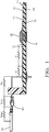
- Figure 1 shows a connection setup from the prior art in a sectional view.
- a semiconductor component 20 is arranged on a printed circuit board 10, the printed circuit board 10 is electrically connected to an electrical conductor 50 via a contact element 40.
- the printed circuit board 10 has a first conductive coating 15 on the first surface 13, a first side 11, and a second conductive coating 16 on a second surface 14, a second side 12.
- the semiconductor component 20 is connected via the electrical conductor 50 , the contact element 40, the conductive coatings 15, 16 with current provided.
- the electrical resistances that oppose the current flow are identified by the reference symbols Rwc, Rcp, Rp, Rpt and Rt. In this illustration it can be clearly seen that the electrical current has to overcome many partial resistances in order to reach the semiconductor components.
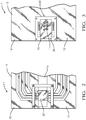
- Figure 2 shows the first page 11 of the inventive connection arrangement.
- a semiconductor component 20 is attached to the first surface 13 and is electrically connected to parts of the first conductive coating 15.
- Figure 3 shows the second side 12 of the inventive connection arrangement.
- the second conductive coating 16 is shown on the second surface 14.
- a connecting means 30 is produced from a portion of the second coating coating 16. This already occurs during the manufacture of the printed circuit board 10.
- the connecting means 30 is produced during the etching or milling of the conductor tracks.
- the shape of the connecting means 30 corresponds to the shape of a contact area 41 of the contact element 40.
- the shape and size of the contact area 41 should be chosen such that the surfaces do not substantially overlap when the contact area 41 is contacted with the connecting means 30. Only where the contact area 41 and the connecting means 30 are connected to one another is electricity and heat optimally transported.
- plated-through holes 17 are shown, which establish an electrical connection between the first electrically conductive coating 15 and the second electrically conductive coating 16.
- the vias 17 are in Figure 2 not visible since they are covered by the semiconductor components 20.
- a holding means 60 which will be explained in more detail later, is also shown in FIG Figure 3 shown.
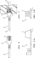
- Figure 4 shows the contact element 40 in a plan view.
- the electrical conductor 50 is connected to the contact element 40 by means of a crimp connection.
- Figure 5 shows the contact element 40 with the electrical conductors 50 attached to it.
- the holding means 60 comprises a clamping profile 61 and an eccentric 62 to which a lever 63 is attached.
- the operation of the holding means 60 is off Figure 7 derivable.
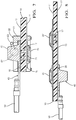
- Figure 6A and 6B show the contact element 40 in side views.
- the flat contact area 41 with which the contact element 40 contacts the connecting means 30 can be seen.
- the contact element 40 has coolant 70 in the form of cooling fins, which extend from the contact area 41, counter to the contact area 41.
- the electrical conductor 50 is attached by means of a crimp connection.
- any known connection technology such as screw connections, soldered or welded connections could be used.
- Figure 7 shows an embodiment of the invention in a sectional view.
- the contact element 40 with the electrical conductor 50 attached to it, is pressed onto the second conductive coating 16 of the circuit board 10 by means of the holding means 60 and is thus electrically contacted via the connecting means 30.
- the contact element 40 and the connecting means 30 are located on the second side 12 of the printed circuit board 10, opposite the semiconductor component 20, which is attached on the first side 11.
- the connecting means 30 has plated-through holes 17 which extend through the printed circuit board 10, from the first conductive coating 15 to the second conductive coating 16 and connect them to one another.
- the semiconductor device 20 has a contact region 21 on the side of the body facing the printed circuit board. The contact region 21 is electrically connected to the first conductive coating 15.
- This structure makes it possible to implement a current path with a low resistance starting from the electrical line 50 to the semiconductor components 20.
- this arrangement offers the possibility of using the contact element 40 and the electrical conductor 50 as cooling elements, since they are in the immediate vicinity, only separated by the printed circuit board, at the heat source (semiconductor component). Due to the close proximity, this arrangement can cool effectively.
- Figure 8 shows an embodiment in which two semiconductor components 20, 20 'are arranged on the first side 11 of the printed circuit board 10.
- the contact element 40 is fixed at a position opposite the first semiconductor component 20.
- the semiconductor component 20 is not intended to control the current that is transported via the electrical conductor 50.
- the contact element 40 is electrically connected to the second semiconductor component 20 ′ via the second conductive coating 16.
- the second semiconductor component 20 ′ controls the current that flows through the electrical conductor 50.
- a semiconductor component 20 is cooled by selecting the position relative to the connecting means 30 and thus the contact element 40, but is not supplied with current.
- the second semiconductor component 20 ′ is supplied with current, but is not cooled by the contact element 40, since it is not opposite the contact element 40. Small compensating heat flows in the conductive coatings 15, 16 are not taken into account here.
Landscapes
- Engineering & Computer Science (AREA)
- Microelectronics & Electronic Packaging (AREA)
- Coupling Device And Connection With Printed Circuit (AREA)
- Cooling Or The Like Of Electrical Apparatus (AREA)
- Multi-Conductor Connections (AREA)
Priority Applications (3)
| Application Number | Priority Date | Filing Date | Title |
|---|---|---|---|
| EP14179926.2A EP2983246B1 (de) | 2014-08-05 | 2014-08-05 | Elektrische Verbindungsanordnung |
| US14/817,791 US9620873B2 (en) | 2014-08-05 | 2015-08-04 | Electrical connection arrangement |
| CN201510581462.1A CN105337100B (zh) | 2014-08-05 | 2015-08-05 | 电连接装置 |
Applications Claiming Priority (1)
| Application Number | Priority Date | Filing Date | Title |
|---|---|---|---|
| EP14179926.2A EP2983246B1 (de) | 2014-08-05 | 2014-08-05 | Elektrische Verbindungsanordnung |
Publications (2)
| Publication Number | Publication Date |
|---|---|
| EP2983246A1 EP2983246A1 (de) | 2016-02-10 |
| EP2983246B1 true EP2983246B1 (de) | 2020-03-04 |
Family
ID=51263333
Family Applications (1)
| Application Number | Title | Priority Date | Filing Date |
|---|---|---|---|
| EP14179926.2A Active EP2983246B1 (de) | 2014-08-05 | 2014-08-05 | Elektrische Verbindungsanordnung |
Country Status (3)
| Country | Link |
|---|---|
| US (1) | US9620873B2 (zh) |
| EP (1) | EP2983246B1 (zh) |
| CN (1) | CN105337100B (zh) |
Families Citing this family (5)
| Publication number | Priority date | Publication date | Assignee | Title |
|---|---|---|---|---|
| DE102016105347A1 (de) * | 2016-03-22 | 2017-09-28 | Phoenix Contact E-Mobility Gmbh | Steckverbinderteil mit einem gekühlten Kontaktelement |
| DE102016105311A1 (de) * | 2016-03-22 | 2017-09-28 | Phoenix Contact E-Mobility Gmbh | Steckverbinderteil mit einem gekühlten Kontaktelement |
| EP3297097A1 (en) * | 2016-09-16 | 2018-03-21 | Delphi Technologies, Inc. | Contact element for a printed circuit board |
| JP2019047029A (ja) * | 2017-09-05 | 2019-03-22 | 矢崎総業株式会社 | 回路基板の放熱構造 |
| US11285832B2 (en) * | 2019-06-05 | 2022-03-29 | TE Connectivity Services Gmbh | Heat exchanger for a power connector |
Citations (1)
| Publication number | Priority date | Publication date | Assignee | Title |
|---|---|---|---|---|
| DE102010062410A1 (de) * | 2010-02-11 | 2011-08-11 | Lear Corporation, Mich. | Elektrischer Stecker und Wärmesenke |
Family Cites Families (23)
| Publication number | Priority date | Publication date | Assignee | Title |
|---|---|---|---|---|
| US4420206A (en) * | 1981-11-30 | 1983-12-13 | Western Electric Company, Inc. | Electrical connector |
| US4645943A (en) * | 1984-10-15 | 1987-02-24 | Dallas Semiconductor Corporation | Space-saving back-up power supply |
| US4935864A (en) * | 1989-06-20 | 1990-06-19 | Digital Equipment Corporation | Localized cooling apparatus for cooling integrated circuit devices |
| US5469330A (en) * | 1994-02-14 | 1995-11-21 | Karabatsos; Chris | Heat sink header assembly |
| US5470795A (en) * | 1994-02-25 | 1995-11-28 | Shushurin; Vladimir V. | Method of connecting terminals of a plastic-encapsulated power transistor to a printed-circuit board |
| TW381328B (en) * | 1994-03-07 | 2000-02-01 | Ibm | Dual substrate package assembly for being electrically coupled to a conducting member |
| US6018465A (en) * | 1996-12-31 | 2000-01-25 | Intel Corporation | Apparatus for mounting a chip package to a chassis of a computer |
| CA2225235A1 (en) * | 1997-12-19 | 1999-06-19 | Northern Telecom Limited | A line interface module |
| US6166464A (en) * | 1998-08-24 | 2000-12-26 | International Rectifier Corp. | Power module |
| JP4131935B2 (ja) * | 2003-02-18 | 2008-08-13 | 株式会社東芝 | インターフェイスモジュールとインターフェイスモジュール付lsiパッケージ及びその実装方法 |
| US8068346B2 (en) * | 2004-05-04 | 2011-11-29 | Hamilton Sundstrand Corporation | Circuit board with high density power semiconductors |
| CN2821902Y (zh) * | 2005-06-29 | 2006-09-27 | 富士康(昆山)电脑接插件有限公司 | 电连接器组件 |
| US8657031B2 (en) * | 2005-10-12 | 2014-02-25 | Black & Decker Inc. | Universal control module |
| FR2895204B1 (fr) * | 2005-12-21 | 2008-06-06 | Valeo Systemes Thermiques | Optimisation d'un dispositif de chauffage |
| US7233502B1 (en) * | 2006-03-15 | 2007-06-19 | Universal Scientific Industrial Co., Ltd. | Twin-substrate wireless electronic module and method for making the same |
| US7510418B1 (en) * | 2007-10-31 | 2009-03-31 | Intel Corporation | Loading mechanisms for integrated circuit (IC) packages |
| CN201126880Y (zh) * | 2007-12-25 | 2008-10-01 | 上海徕木电子有限公司 | 一种电子线路板的连接器 |
| DE102008040290A1 (de) * | 2008-07-09 | 2010-01-14 | Robert Bosch Gmbh | Hybridschaltungsstruktur mit keramischen Schaltungsträgern |
| TWI387090B (zh) * | 2009-06-05 | 2013-02-21 | Walton Advanced Eng Inc | Reverse staggered stack structure of integrated circuit module |
| US8724339B2 (en) * | 2009-12-01 | 2014-05-13 | Apple Inc. | Compact media player |
| TWI406390B (zh) * | 2010-02-26 | 2013-08-21 | Walton Advanced Eng Inc | High density integrated circuit module structure |
| US8572840B2 (en) * | 2010-09-30 | 2013-11-05 | International Business Machines Corporation | Method of attaching an electronic module power supply |
| JP5582995B2 (ja) * | 2010-12-14 | 2014-09-03 | 新光電気工業株式会社 | ソケット |
-
2014
- 2014-08-05 EP EP14179926.2A patent/EP2983246B1/de active Active
-
2015
- 2015-08-04 US US14/817,791 patent/US9620873B2/en active Active
- 2015-08-05 CN CN201510581462.1A patent/CN105337100B/zh active Active
Patent Citations (1)
| Publication number | Priority date | Publication date | Assignee | Title |
|---|---|---|---|---|
| DE102010062410A1 (de) * | 2010-02-11 | 2011-08-11 | Lear Corporation, Mich. | Elektrischer Stecker und Wärmesenke |
Also Published As
| Publication number | Publication date |
|---|---|
| CN105337100A (zh) | 2016-02-17 |
| US9620873B2 (en) | 2017-04-11 |
| US20160043485A1 (en) | 2016-02-11 |
| CN105337100B (zh) | 2017-12-19 |
| EP2983246A1 (de) | 2016-02-10 |
Similar Documents
| Publication | Publication Date | Title |
|---|---|---|
| EP2983246B1 (de) | Elektrische Verbindungsanordnung | |
| DE102013225411B4 (de) | Verbinder für eine LED-Modulplatine und Kombination aus Verbinder und LED- Modulplatine | |
| DE112006002302B4 (de) | Elektrisches system umfassend eine leistungstransistoranordnung, eine stromschiene und eine leiterplattenbaugruppe | |
| DE102015103096B4 (de) | Kühleinrichtung und Kühlanordnung mit der Kühleinrichtung | |
| DE102010062410A1 (de) | Elektrischer Stecker und Wärmesenke | |
| DE102017219229B4 (de) | Verzweigungsstruktur und Kabelbaum | |
| EP3095307B1 (de) | Leiterplatte, schaltung und verfahren zur herstellung einer schaltung | |
| DE102012216694A1 (de) | Elektrische Verbindung mit Kühlung zur Wärmeableitung | |
| DE112015002187T5 (de) | Schaltungsbaugruppe und elektrischer Verteiler | |
| DE102014203737B4 (de) | Elektronisches teil und elektronische steuereinheit | |
| DE102013221635A1 (de) | Elektronisches Gerät | |
| DE112016004181T5 (de) | Schaltungsanordnung und elektrischer Verteilerkasten | |
| DE19518522C2 (de) | Steuergerät für ein Kraftfahrzeug | |
| DE102011088322A1 (de) | Verbindungssystem zum elektrischen Anschließen elektrischer Geräte und Verfahren zum Verbinden eines elektrisch leitenden ersten Anschlusses und eines elektrisch leitenden zweiten Anschlusses | |
| EP2716145B1 (de) | Leiterplatte für elektrische bauelemente und leiterplattensystem | |
| DE102015104297B4 (de) | Fixierelement zum Anbinden einer Platine, Stromschiene und damit ausgestatteter Stromverteiler eines Fahrzeugs | |
| DE102010008074A1 (de) | Gehäuse mit Kühlvorrichtung | |
| DE102020100856A1 (de) | Direktstecksystem für die Verbindung eines Steckverbinders mit einer Leiterplatte | |
| DE102013007167B4 (de) | Hochstromsteckverbindung mit Wärmeabfuhrelementen | |
| EP2006910A2 (de) | Leistungselektronikmodul | |
| DE102015220096B4 (de) | Elektrische Kontaktverbindung und elektrischer Kontakt | |
| DE102017125687B3 (de) | Dezentraler kleinverteiler, leitungssystem und herstellverfahren | |
| EP3251472B1 (de) | Elektrogerät, baureihe von elektrogeräten und verfahren zur herstellung | |
| EP3881652A1 (de) | Schaltungsträger, (leistungs-)elektronikanordnung und elektrische antriebsvorrichtung | |
| DE102020216305B4 (de) | Elektrische Schaltvorrichtung |
Legal Events
| Date | Code | Title | Description |
|---|---|---|---|
| PUAI | Public reference made under article 153(3) epc to a published international application that has entered the european phase |
Free format text: ORIGINAL CODE: 0009012 |
|
| AK | Designated contracting states |
Kind code of ref document: A1 Designated state(s): AL AT BE BG CH CY CZ DE DK EE ES FI FR GB GR HR HU IE IS IT LI LT LU LV MC MK MT NL NO PL PT RO RS SE SI SK SM TR |
|
| AX | Request for extension of the european patent |
Extension state: BA ME |
|
| 17P | Request for examination filed |
Effective date: 20160810 |
|
| RBV | Designated contracting states (corrected) |
Designated state(s): AL AT BE BG CH CY CZ DE DK EE ES FI FR GB GR HR HU IE IS IT LI LT LU LV MC MK MT NL NO PL PT RO RS SE SI SK SM TR |
|
| STAA | Information on the status of an ep patent application or granted ep patent |
Free format text: STATUS: EXAMINATION IS IN PROGRESS |
|
| 17Q | First examination report despatched |
Effective date: 20180105 |
|
| RAP1 | Party data changed (applicant data changed or rights of an application transferred) |
Owner name: APTIV TECHNOLOGIES LIMITED |
|
| GRAP | Despatch of communication of intention to grant a patent |
Free format text: ORIGINAL CODE: EPIDOSNIGR1 |
|
| STAA | Information on the status of an ep patent application or granted ep patent |
Free format text: STATUS: GRANT OF PATENT IS INTENDED |
|
| RIC1 | Information provided on ipc code assigned before grant |
Ipc: H01R 12/70 20110101ALN20190820BHEP Ipc: H01R 12/88 20110101ALN20190820BHEP Ipc: H01R 12/71 20110101AFI20190820BHEP Ipc: H01R 12/75 20110101ALI20190820BHEP Ipc: H05K 1/02 20060101ALI20190820BHEP |
|
| INTG | Intention to grant announced |
Effective date: 20190918 |
|
| GRAS | Grant fee paid |
Free format text: ORIGINAL CODE: EPIDOSNIGR3 |
|
| GRAA | (expected) grant |
Free format text: ORIGINAL CODE: 0009210 |
|
| STAA | Information on the status of an ep patent application or granted ep patent |
Free format text: STATUS: THE PATENT HAS BEEN GRANTED |
|
| AK | Designated contracting states |
Kind code of ref document: B1 Designated state(s): AL AT BE BG CH CY CZ DE DK EE ES FI FR GB GR HR HU IE IS IT LI LT LU LV MC MK MT NL NO PL PT RO RS SE SI SK SM TR |
|
| REG | Reference to a national code |
Ref country code: GB Ref legal event code: FG4D Free format text: NOT ENGLISH |
|
| REG | Reference to a national code |
Ref country code: CH Ref legal event code: EP |
|
| REG | Reference to a national code |
Ref country code: AT Ref legal event code: REF Ref document number: 1241452 Country of ref document: AT Kind code of ref document: T Effective date: 20200315 |
|
| REG | Reference to a national code |
Ref country code: DE Ref legal event code: R096 Ref document number: 502014013727 Country of ref document: DE |
|
| REG | Reference to a national code |
Ref country code: IE Ref legal event code: FG4D Free format text: LANGUAGE OF EP DOCUMENT: GERMAN |
|
| PG25 | Lapsed in a contracting state [announced via postgrant information from national office to epo] |
Ref country code: NO Free format text: LAPSE BECAUSE OF FAILURE TO SUBMIT A TRANSLATION OF THE DESCRIPTION OR TO PAY THE FEE WITHIN THE PRESCRIBED TIME-LIMIT Effective date: 20200604 Ref country code: FI Free format text: LAPSE BECAUSE OF FAILURE TO SUBMIT A TRANSLATION OF THE DESCRIPTION OR TO PAY THE FEE WITHIN THE PRESCRIBED TIME-LIMIT Effective date: 20200304 Ref country code: RS Free format text: LAPSE BECAUSE OF FAILURE TO SUBMIT A TRANSLATION OF THE DESCRIPTION OR TO PAY THE FEE WITHIN THE PRESCRIBED TIME-LIMIT Effective date: 20200304 |
|
| REG | Reference to a national code |
Ref country code: NL Ref legal event code: MP Effective date: 20200304 |
|
| PG25 | Lapsed in a contracting state [announced via postgrant information from national office to epo] |
Ref country code: GR Free format text: LAPSE BECAUSE OF FAILURE TO SUBMIT A TRANSLATION OF THE DESCRIPTION OR TO PAY THE FEE WITHIN THE PRESCRIBED TIME-LIMIT Effective date: 20200605 Ref country code: SE Free format text: LAPSE BECAUSE OF FAILURE TO SUBMIT A TRANSLATION OF THE DESCRIPTION OR TO PAY THE FEE WITHIN THE PRESCRIBED TIME-LIMIT Effective date: 20200304 Ref country code: LV Free format text: LAPSE BECAUSE OF FAILURE TO SUBMIT A TRANSLATION OF THE DESCRIPTION OR TO PAY THE FEE WITHIN THE PRESCRIBED TIME-LIMIT Effective date: 20200304 Ref country code: HR Free format text: LAPSE BECAUSE OF FAILURE TO SUBMIT A TRANSLATION OF THE DESCRIPTION OR TO PAY THE FEE WITHIN THE PRESCRIBED TIME-LIMIT Effective date: 20200304 Ref country code: BG Free format text: LAPSE BECAUSE OF FAILURE TO SUBMIT A TRANSLATION OF THE DESCRIPTION OR TO PAY THE FEE WITHIN THE PRESCRIBED TIME-LIMIT Effective date: 20200604 |
|
| REG | Reference to a national code |
Ref country code: LT Ref legal event code: MG4D |
|
| PG25 | Lapsed in a contracting state [announced via postgrant information from national office to epo] |
Ref country code: NL Free format text: LAPSE BECAUSE OF FAILURE TO SUBMIT A TRANSLATION OF THE DESCRIPTION OR TO PAY THE FEE WITHIN THE PRESCRIBED TIME-LIMIT Effective date: 20200304 |
|
| PG25 | Lapsed in a contracting state [announced via postgrant information from national office to epo] |
Ref country code: EE Free format text: LAPSE BECAUSE OF FAILURE TO SUBMIT A TRANSLATION OF THE DESCRIPTION OR TO PAY THE FEE WITHIN THE PRESCRIBED TIME-LIMIT Effective date: 20200304 Ref country code: LT Free format text: LAPSE BECAUSE OF FAILURE TO SUBMIT A TRANSLATION OF THE DESCRIPTION OR TO PAY THE FEE WITHIN THE PRESCRIBED TIME-LIMIT Effective date: 20200304 Ref country code: SK Free format text: LAPSE BECAUSE OF FAILURE TO SUBMIT A TRANSLATION OF THE DESCRIPTION OR TO PAY THE FEE WITHIN THE PRESCRIBED TIME-LIMIT Effective date: 20200304 Ref country code: ES Free format text: LAPSE BECAUSE OF FAILURE TO SUBMIT A TRANSLATION OF THE DESCRIPTION OR TO PAY THE FEE WITHIN THE PRESCRIBED TIME-LIMIT Effective date: 20200304 Ref country code: IS Free format text: LAPSE BECAUSE OF FAILURE TO SUBMIT A TRANSLATION OF THE DESCRIPTION OR TO PAY THE FEE WITHIN THE PRESCRIBED TIME-LIMIT Effective date: 20200704 Ref country code: CZ Free format text: LAPSE BECAUSE OF FAILURE TO SUBMIT A TRANSLATION OF THE DESCRIPTION OR TO PAY THE FEE WITHIN THE PRESCRIBED TIME-LIMIT Effective date: 20200304 Ref country code: RO Free format text: LAPSE BECAUSE OF FAILURE TO SUBMIT A TRANSLATION OF THE DESCRIPTION OR TO PAY THE FEE WITHIN THE PRESCRIBED TIME-LIMIT Effective date: 20200304 Ref country code: PT Free format text: LAPSE BECAUSE OF FAILURE TO SUBMIT A TRANSLATION OF THE DESCRIPTION OR TO PAY THE FEE WITHIN THE PRESCRIBED TIME-LIMIT Effective date: 20200729 Ref country code: SM Free format text: LAPSE BECAUSE OF FAILURE TO SUBMIT A TRANSLATION OF THE DESCRIPTION OR TO PAY THE FEE WITHIN THE PRESCRIBED TIME-LIMIT Effective date: 20200304 |
|
| REG | Reference to a national code |
Ref country code: DE Ref legal event code: R097 Ref document number: 502014013727 Country of ref document: DE |
|
| PLBE | No opposition filed within time limit |
Free format text: ORIGINAL CODE: 0009261 |
|
| STAA | Information on the status of an ep patent application or granted ep patent |
Free format text: STATUS: NO OPPOSITION FILED WITHIN TIME LIMIT |
|
| PG25 | Lapsed in a contracting state [announced via postgrant information from national office to epo] |
Ref country code: DK Free format text: LAPSE BECAUSE OF FAILURE TO SUBMIT A TRANSLATION OF THE DESCRIPTION OR TO PAY THE FEE WITHIN THE PRESCRIBED TIME-LIMIT Effective date: 20200304 Ref country code: IT Free format text: LAPSE BECAUSE OF FAILURE TO SUBMIT A TRANSLATION OF THE DESCRIPTION OR TO PAY THE FEE WITHIN THE PRESCRIBED TIME-LIMIT Effective date: 20200304 |
|
| 26N | No opposition filed |
Effective date: 20201207 |
|
| PG25 | Lapsed in a contracting state [announced via postgrant information from national office to epo] |
Ref country code: SI Free format text: LAPSE BECAUSE OF FAILURE TO SUBMIT A TRANSLATION OF THE DESCRIPTION OR TO PAY THE FEE WITHIN THE PRESCRIBED TIME-LIMIT Effective date: 20200304 Ref country code: PL Free format text: LAPSE BECAUSE OF FAILURE TO SUBMIT A TRANSLATION OF THE DESCRIPTION OR TO PAY THE FEE WITHIN THE PRESCRIBED TIME-LIMIT Effective date: 20200304 |
|
| PG25 | Lapsed in a contracting state [announced via postgrant information from national office to epo] |
Ref country code: MC Free format text: LAPSE BECAUSE OF FAILURE TO SUBMIT A TRANSLATION OF THE DESCRIPTION OR TO PAY THE FEE WITHIN THE PRESCRIBED TIME-LIMIT Effective date: 20200304 |
|
| REG | Reference to a national code |
Ref country code: CH Ref legal event code: PL |
|
| PG25 | Lapsed in a contracting state [announced via postgrant information from national office to epo] |
Ref country code: LU Free format text: LAPSE BECAUSE OF NON-PAYMENT OF DUE FEES Effective date: 20200805 Ref country code: LI Free format text: LAPSE BECAUSE OF NON-PAYMENT OF DUE FEES Effective date: 20200831 Ref country code: CH Free format text: LAPSE BECAUSE OF NON-PAYMENT OF DUE FEES Effective date: 20200831 |
|
| REG | Reference to a national code |
Ref country code: BE Ref legal event code: MM Effective date: 20200831 |
|
| PG25 | Lapsed in a contracting state [announced via postgrant information from national office to epo] |
Ref country code: BE Free format text: LAPSE BECAUSE OF NON-PAYMENT OF DUE FEES Effective date: 20200831 Ref country code: IE Free format text: LAPSE BECAUSE OF NON-PAYMENT OF DUE FEES Effective date: 20200805 |
|
| REG | Reference to a national code |
Ref country code: AT Ref legal event code: MM01 Ref document number: 1241452 Country of ref document: AT Kind code of ref document: T Effective date: 20200805 |
|
| PG25 | Lapsed in a contracting state [announced via postgrant information from national office to epo] |
Ref country code: AT Free format text: LAPSE BECAUSE OF NON-PAYMENT OF DUE FEES Effective date: 20200805 |
|
| PG25 | Lapsed in a contracting state [announced via postgrant information from national office to epo] |
Ref country code: TR Free format text: LAPSE BECAUSE OF FAILURE TO SUBMIT A TRANSLATION OF THE DESCRIPTION OR TO PAY THE FEE WITHIN THE PRESCRIBED TIME-LIMIT Effective date: 20200304 Ref country code: MT Free format text: LAPSE BECAUSE OF FAILURE TO SUBMIT A TRANSLATION OF THE DESCRIPTION OR TO PAY THE FEE WITHIN THE PRESCRIBED TIME-LIMIT Effective date: 20200304 Ref country code: CY Free format text: LAPSE BECAUSE OF FAILURE TO SUBMIT A TRANSLATION OF THE DESCRIPTION OR TO PAY THE FEE WITHIN THE PRESCRIBED TIME-LIMIT Effective date: 20200304 |
|
| PG25 | Lapsed in a contracting state [announced via postgrant information from national office to epo] |
Ref country code: MK Free format text: LAPSE BECAUSE OF FAILURE TO SUBMIT A TRANSLATION OF THE DESCRIPTION OR TO PAY THE FEE WITHIN THE PRESCRIBED TIME-LIMIT Effective date: 20200304 Ref country code: AL Free format text: LAPSE BECAUSE OF FAILURE TO SUBMIT A TRANSLATION OF THE DESCRIPTION OR TO PAY THE FEE WITHIN THE PRESCRIBED TIME-LIMIT Effective date: 20200304 |
|
| P01 | Opt-out of the competence of the unified patent court (upc) registered |
Effective date: 20230424 |
|
| PGFP | Annual fee paid to national office [announced via postgrant information from national office to epo] |
Ref country code: GB Payment date: 20230822 Year of fee payment: 10 |
|
| PGFP | Annual fee paid to national office [announced via postgrant information from national office to epo] |
Ref country code: FR Payment date: 20230821 Year of fee payment: 10 Ref country code: DE Payment date: 20230817 Year of fee payment: 10 |