EP2966683A1 - Semiconductor device - Google Patents
Semiconductor device Download PDFInfo
- Publication number
- EP2966683A1 EP2966683A1 EP14850425.1A EP14850425A EP2966683A1 EP 2966683 A1 EP2966683 A1 EP 2966683A1 EP 14850425 A EP14850425 A EP 14850425A EP 2966683 A1 EP2966683 A1 EP 2966683A1
- Authority
- EP
- European Patent Office
- Prior art keywords
- region
- type
- trench
- anode
- igbt
- Prior art date
- Legal status (The legal status is an assumption and is not a legal conclusion. Google has not performed a legal analysis and makes no representation as to the accuracy of the status listed.)
- Granted
Links
Images








Classifications
-
- H—ELECTRICITY
- H10—SEMICONDUCTOR DEVICES; ELECTRIC SOLID-STATE DEVICES NOT OTHERWISE PROVIDED FOR
- H10D—INORGANIC ELECTRIC SEMICONDUCTOR DEVICES
- H10D84/00—Integrated devices formed in or on semiconductor substrates that comprise only semiconducting layers, e.g. on Si wafers or on GaAs-on-Si wafers
- H10D84/60—Integrated devices formed in or on semiconductor substrates that comprise only semiconducting layers, e.g. on Si wafers or on GaAs-on-Si wafers characterised by the integration of at least one component covered by groups H10D10/00 or H10D18/00, e.g. integration of BJTs
- H10D84/611—Combinations of BJTs and one or more of diodes, resistors or capacitors
- H10D84/613—Combinations of vertical BJTs and one or more of diodes, resistors or capacitors
- H10D84/617—Combinations of vertical BJTs and only diodes
-
- H—ELECTRICITY
- H10—SEMICONDUCTOR DEVICES; ELECTRIC SOLID-STATE DEVICES NOT OTHERWISE PROVIDED FOR
- H10D—INORGANIC ELECTRIC SEMICONDUCTOR DEVICES
- H10D12/00—Bipolar devices controlled by the field effect, e.g. insulated-gate bipolar transistors [IGBT]
- H10D12/01—Manufacture or treatment
- H10D12/031—Manufacture or treatment of IGBTs
- H10D12/032—Manufacture or treatment of IGBTs of vertical IGBTs
- H10D12/038—Manufacture or treatment of IGBTs of vertical IGBTs having a recessed gate, e.g. trench-gate IGBTs
-
- H—ELECTRICITY
- H10—SEMICONDUCTOR DEVICES; ELECTRIC SOLID-STATE DEVICES NOT OTHERWISE PROVIDED FOR
- H10D—INORGANIC ELECTRIC SEMICONDUCTOR DEVICES
- H10D12/00—Bipolar devices controlled by the field effect, e.g. insulated-gate bipolar transistors [IGBT]
- H10D12/411—Insulated-gate bipolar transistors [IGBT]
- H10D12/441—Vertical IGBTs
- H10D12/461—Vertical IGBTs having non-planar surfaces, e.g. having trenches, recesses or pillars in the surfaces of the emitter, base or collector regions
- H10D12/481—Vertical IGBTs having non-planar surfaces, e.g. having trenches, recesses or pillars in the surfaces of the emitter, base or collector regions having gate structures on slanted surfaces, on vertical surfaces, or in grooves, e.g. trench gate IGBTs
-
- H—ELECTRICITY
- H10—SEMICONDUCTOR DEVICES; ELECTRIC SOLID-STATE DEVICES NOT OTHERWISE PROVIDED FOR
- H10D—INORGANIC ELECTRIC SEMICONDUCTOR DEVICES
- H10D62/00—Semiconductor bodies, or regions thereof, of devices having potential barriers
- H10D62/10—Shapes, relative sizes or dispositions of the regions of the semiconductor bodies; Shapes of the semiconductor bodies
- H10D62/124—Shapes, relative sizes or dispositions of the regions of semiconductor bodies or of junctions between the regions
- H10D62/126—Top-view geometrical layouts of the regions or the junctions
- H10D62/127—Top-view geometrical layouts of the regions or the junctions of cellular field-effect devices, e.g. multicellular DMOS transistors or IGBTs
-
- H—ELECTRICITY
- H10—SEMICONDUCTOR DEVICES; ELECTRIC SOLID-STATE DEVICES NOT OTHERWISE PROVIDED FOR
- H10D—INORGANIC ELECTRIC SEMICONDUCTOR DEVICES
- H10D62/00—Semiconductor bodies, or regions thereof, of devices having potential barriers
- H10D62/10—Shapes, relative sizes or dispositions of the regions of the semiconductor bodies; Shapes of the semiconductor bodies
- H10D62/13—Semiconductor regions connected to electrodes carrying current to be rectified, amplified or switched, e.g. source or drain regions
- H10D62/141—Anode or cathode regions of thyristors; Collector or emitter regions of gated bipolar-mode devices, e.g. of IGBTs
- H10D62/142—Anode regions of thyristors or collector regions of gated bipolar-mode devices
-
- H—ELECTRICITY
- H10—SEMICONDUCTOR DEVICES; ELECTRIC SOLID-STATE DEVICES NOT OTHERWISE PROVIDED FOR
- H10D—INORGANIC ELECTRIC SEMICONDUCTOR DEVICES
- H10D62/00—Semiconductor bodies, or regions thereof, of devices having potential barriers
- H10D62/10—Shapes, relative sizes or dispositions of the regions of the semiconductor bodies; Shapes of the semiconductor bodies
- H10D62/17—Semiconductor regions connected to electrodes not carrying current to be rectified, amplified or switched, e.g. channel regions
- H10D62/393—Body regions of DMOS transistors or IGBTs
-
- H—ELECTRICITY
- H10—SEMICONDUCTOR DEVICES; ELECTRIC SOLID-STATE DEVICES NOT OTHERWISE PROVIDED FOR
- H10D—INORGANIC ELECTRIC SEMICONDUCTOR DEVICES
- H10D62/00—Semiconductor bodies, or regions thereof, of devices having potential barriers
- H10D62/80—Semiconductor bodies, or regions thereof, of devices having potential barriers characterised by the materials
- H10D62/83—Semiconductor bodies, or regions thereof, of devices having potential barriers characterised by the materials being Group IV materials, e.g. B-doped Si or undoped Ge
-
- H—ELECTRICITY
- H10—SEMICONDUCTOR DEVICES; ELECTRIC SOLID-STATE DEVICES NOT OTHERWISE PROVIDED FOR
- H10D—INORGANIC ELECTRIC SEMICONDUCTOR DEVICES
- H10D64/00—Electrodes of devices having potential barriers
- H10D64/60—Electrodes characterised by their materials
- H10D64/62—Electrodes ohmically coupled to a semiconductor
Definitions
- the present invention relates to a semiconductor device.
- MOS power device driven by a MOS gate is commonly known as a power semiconductor device wherein increasing current and reducing loss are possible.
- MOS gate structures of the MOS power device Two kinds of structure are widely known as MOS gate structures of the MOS power device, those being a planar gate structure, wherein a MOS gate is provided in plate form on a semiconductor substrate, and a trench gate structure, wherein a MOS gate is embedded in a trench formed in a semiconductor substrate.
- the trench gate structure is attracting attention in recent vertical power devices, as the structure thereof is such that low on-state resistance characteristics are easily obtained.
- RC-IGBT reverse conducting IGBT
- IGBT insulated gate bipolar transistor
- FWD freewheeling diode
- Fig. 18 is a plan view showing the structure of the existing RC-IGBT.
- Fig. 19 is a sectional view showing the sectional structure along a cutting line AA-AA' of Fig. 18 .
- the existing RC-IGBT includes a general field stop IGBT (FS-IGBT) and an FWD connected in anti-parallel to the FS-IGBT on the same n - -type semiconductor substrate, which forms an n - -type drift region 101.
- FS-IGBT general field stop IGBT
- FWD field stop IGBT
- an RC-IGBT has a structure wherein, taking a p-type base region configuring a MOS gate structure on the front surface side of an n - -type semiconductor substrate to be a p-type anode region 105-2, one portion of a p + -type collector region 111 provided on the back surface side of the n - -type semiconductor substrate is replaced with an n + -type cathode region 112.
- an IGBT portion 121 in which an FS-IGBT is provided and an FWD portion 122 in which an FWD is provided are provided on the same n - -type semiconductor substrate.
- a trench gate type MOS gate structure formed of a trench 102, gate insulating film 103, gate electrode 104, p-type base region 105-1, n + -type emitter region 106, and p + -type contact region 107, and an emitter electrode 109, are provided on the front surface side of the n - -type semiconductor substrate in the IGBT portion 121.
- the p-type base region 105-1 is disposed at predetermined intervals in the longitudinal direction of the trench 102 in a mesa portion (a region sandwiched between neighboring trenches 102) between neighboring trenches 102.
- the trench gate formed of the trench 102, gate insulating film 103, and gate electrode 104 is provided in a stripe form extending in a direction (the longitudinal direction) perpendicular to the direction in which the IGBT portion 121 and FWB portion 122 are aligned (the lateral direction) from the IGBT portion 121 across the FWB portion 122.
- the p-type anode region 105-2 is provided over the whole of the front surface of the n - -type semiconductor substrate in a mesa portion between neighboring trenches 102 in the FWD portion 122.
- the p-type anode region 105-2 is conductively connected to the emitter electrode 109.
- the p + -type collector region 111 is provided in the IGBT portion 121 and the n + -type cathode region 112 is provided in the FWD portion 122.
- An n-type buffer layer 110 is provided between the p + -type collector region 111 and n + -type cathode region 112 and the n - -type drift region 101.
- a collector electrode 113 is in contact with the p + -type collector region 111 and n + -type cathode region 112.
- Reference sign 108 is an interlayer dielectric.
- a collector short device wherein a MOS gate structure is repeatedly disposed in a pattern the same as that of a normal IGBT on the front surface of a semiconductor chip, and an FWD portion n + -type cathode region and IGBT portion p + -type collector region are disposed in parallel on the back surface of the semiconductor chip, has been proposed as this kind of RC-IGBT (for example, refer to PTL 2).
- a device of a structure wherein an emitter layer is provided in a first region on a first main surface side of a semiconductor substrate but no emitter layer is provided in a second region and of a structure wherein a collector layer is provided in a first region on a second main surface side of the semiconductor substrate and a cathode layer is provided in a second region, has been proposed as another RC-IGBT (for example, refer to PTL 4).
- a device wherein multiple trench gates are formed at differing intervals on a substrate front surface side of a diode portion, and furthermore, an n-type emitter region and p-type base region are formed between trench gates formed at a shorter interval, has been proposed as another RC-IGBT (for example, refer to PTL 5).
- a semiconductor device that is a vertical diode including trenches on a substrate front surface side, wherein the trenches are disposed at differing intervals, and includes two regions, those being a region in which the intervals between trenches in the lateral direction of the trench are long and a region in which the intervals are short, has been proposed as a device including a mesa portion (for example, refer to PTL 6).
- Barrier metal is formed using titanium (Ti), tungsten (W), or the like on the surface of an interlayer dielectric and the inner surface of a second trench.
- An emitter (anode) electrode is in contact with a p-type base (anode) layer, an n-type emitter region, and a p-type contact region via the barrier metal (for example, refer to PTL 7 (Paragraphs 0054 and 0080, Fig. 5 )).
- a back surface electrode is formed on a second main surface so as to be in contact with both a p-type collector region and an n-type cathode region, and has a titanium layer, a nickel (Ni) layer, and a gold (Au) layer stacked sequentially from the second main surface side.
- the titanium layer forms ohmic contact to both the p-type collector region and n-type cathode region (for example, refer to PTL 8).
- a floating layer deeper than an emitter region and contact region in a trench depth direction is provided in a p-type base layer of an IGBT portion.
- No floating layer or emitter region is provided in a diode portion.
- a gate electrode of the diode portion is of the emitter potential (for example, refer to PTL 10). In PTL 10, excessive hole implantation from the contact region of the IGBT portion to the diode portion is prevented by providing the floating layer.
- the heretofore described existing technology is such that trenches are disposed at a comparatively short pitch in an IGBT portion in a stripe form extending in a direction perpendicular to the direction in which the trenches are aligned. Therefore, when no trench is provided penetrating a Schottky junction of a p-type anode region (p-type base region) and n - -type drift layer from the substrate front surface in an FWD portion, there is a problem in that electrical field intensity concentrates in a bottom portion of a trench provided farthest to the FWD portion side in the IGBT portion in an off-state, and breakdown voltage decreases.
- the invention in order to resolve the problems of the heretofore described existing technology, has an object of providing a semiconductor device such that diode characteristics can be improved in a reverse conducting semiconductor device of a structure wherein an insulated gate bipolar transistor and a diode are integrated by being incorporated in the same semiconductor substrate.
- a semiconductor device is a semiconductor device including a first element region in which an insulated gate bipolar transistor is provided and a second element region in which a diode is provided on a semiconductor substrate that forms a first conductivity type drift region, and has the following characteristics.
- a plurality of trenches are provided in stripe form extending in a longitudinal direction perpendicular to the direction in which the first element region and second element region are aligned from the first element region across the second element region in the front surface of the semiconductor substrate.
- a gate insulating film is provided along the side walls and bottom surface of the trench.
- a gate electrode is provided on the inner side of the gate insulating film inside the trench.
- a second conductivity type base region is selectively provided in a mesa portion between neighboring trenches of the first element region.
- a second conductivity type anode region is selectively provided in a mesa portion between neighboring trenches of the second element region.
- a first conductivity type emitter region is selectively provided inside the base region.
- a first electrode in contact with the base region, emitter region, and anode region is provided.
- a second conductivity type collector region is provided on the back surface of the semiconductor substrate in the first element region.
- a first conductivity type cathode region is provided on the back surface of the semiconductor substrate in the second element region.
- a second electrode in contact with the collector region and cathode region is provided.
- the anode region and drift region are repeatedly, alternately disposed in the trench longitudinal direction in a mesa portion between neighboring trenches of the second element region.
- the proportion occupied by the anode region of a unit region formed of the anode region and the drift region in a portion sandwiched by the anode region and the anode region neighboring the anode region in the trench longitudinal direction is 50% or more and less than 100%.
- the heretofore described semiconductor device according to the invention is characterized in that built-in depletion layers spreading into the mesa portion from each of neighboring anode regions are linked to each other.
- a semiconductor device is a semiconductor device including a first element region in which an insulated gate bipolar transistor is provided and a second element region in which a diode is provided on a semiconductor substrate that forms a first conductivity type drift region, and has the following characteristics.
- a plurality of trenches are provided in stripe form extending in a longitudinal direction perpendicular to the direction in which the first element region and second element region are aligned from the first element region across the second element region in the front surface of the semiconductor substrate.
- a gate insulating film is provided along the side walls and bottom surface of the trench.
- a gate electrode is provided on the inner side of the gate insulating film inside the trench.
- a second conductivity type base region is selectively provided in a mesa portion between neighboring trenches of the first element region.
- a second conductivity type anode region is selectively provided in a mesa portion between neighboring trenches of the second element region.
- a first conductivity type emitter region is selectively provided inside the base region.
- a first electrode in contact with the base region, emitter region, and anode region is provided.
- a second conductivity type collector region is provided on the back surface of the semiconductor substrate in the first element region.
- a first conductivity type cathode region is provided on the back surface of the semiconductor substrate in the second element region.
- a second electrode in contact with the collector region and cathode region is provided.
- the anode region and drift region are repeatedly, alternately disposed in the trench longitudinal direction in a mesa portion between neighboring trenches of the second element region.
- the first electrode is further in contact with the drift region in the second element region.
- the proportion occupied by the anode region of a unit region formed of the anode region and the drift region in a portion sandwiched by the anode region and the anode region neighboring the anode region in the trench longitudinal direction is less than 50%.
- the heretofore described semiconductor device according to the invention is characterized in that built-in depletion layers spreading from each of neighboring trenches into a mesa portion between the trenches are linked to each other.
- the semiconductor device According to the semiconductor device according to the invention, there is an advantage in that reverse recovery current can be reduced, and reverse recovery loss can thus be reduced, in a reverse conducting semiconductor device of a structure wherein an insulated gate bipolar transistor and a diode are integrated by being incorporated in the same semiconductor substrate, because of which diode characteristics can be improved.
- n or p in the specifications or attached drawings means that electrons or holes respectively are majority carriers.
- + or - attached to n or p indicates a higher impurity concentration or lower impurity concentration respectively than in a layer or region to which neither is attached.
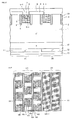
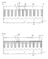
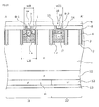
- Fig. 1 is a plan view showing the structure of the semiconductor device according to Embodiment 1.
- Fig. 2 is a sectional view showing the sectional structure along a cutting line A-A' of Fig. 1 .
- the semiconductor device according to Embodiment 1 includes an IGBT portion 21, in which an insulated gate bipolar transistor (IGBT) is provided, and an FWD portion 22, in which a freewheeling diode (FWD) is provided, on the same n - -type semiconductor substrate, which forms an n - -type drift region 1.
- IGBT insulated gate bipolar transistor
- FWD freewheeling diode
- the FWD of the FWD portion 22 is connected in anti-parallel to the IGBT of the IGBT portion 21. That is, the semiconductor device according to Embodiment 1 is a reverse conducting IGBT (RC-IGBT).
- RC-IGBT reverse conducting IGBT
- a multiple of a trench 2 are provided at predetermined intervals in a stripe form extending in a direction (the longitudinal direction) perpendicular to the direction in which the IGBT portion 21 and FWB portion 22 are aligned (the lateral direction), from the IGBT portion 21 across the FWB portion 22, on the front surface of the n - -type semiconductor substrate.
- a gate insulating film 3 is provided inside the trench 2 along the inner wall of the trench 2. Also, a gate electrode 4 is provided on the inner side of the gate insulating film 3 inside the trench 2.
- a p-type base region 5-1 is provided at predetermined intervals in the trench 2 longitudinal direction in a mesa portion between neighboring trenches 2. The p-type base region 5-1 is provided so as to be in contact with the trench 2, and to a depth (a depth from the substrate front surface) less than that of the trench 2.
- the p-type base region 5-1 and n - -type drift region 1 are alternately exposed in the trench 2 longitudinal direction on the front surface of the ri -type semiconductor substrate.
- a width x11 in the trench 2 longitudinal direction of the p-type base region 5-1 is greater than the width in the trench 2 longitudinal direction of a portion of the n - -type drift region 1 sandwiched by the p-type base region 5-1, that is, a first pitch (disposition interval) x12 in the trench 2 longitudinal direction of the p-type base region 5-1 (x11 > x12).
- An n + -type emitter region 6 and a p + -type contact region 7 are selectively provided inside the p-type base region 5-1.
- the n + -type emitter region 6 is in contact with the gate insulating film 3 provided on the side walls of the trench 2, and opposes the gate electrode 4 across the gate insulating film 3.
- the n + -type emitter region 6 is formed of, for example, a first n + -type region 6-1, provided on the side of each trench 2 sandwiching the p-type base region 5-1, and a second n + -type region 6-2 provided between first n + -type regions 6-1 and linking the first n + -type regions 6-1.
- the trench 2 longitudinal direction width of the second n + -type region 6-2 is, for example, less than the trench 2 longitudinal direction width of the first n + -type region 6-1, whereby the n + -type emitter region 6 has, for example, an H-shaped planar form.
- the p + -type contact region 7 is provided between first n + -type regions 6-1, and in contact with the n + -type emitter region 6.
- the IGBT portion 21 on the front surface side of the n - -type semiconductor substrate is of a structure wherein, with the p-type base region 5-1 disposed thinned out, a trench gate type MOS gate structure formed of the trench 2, gate insulating film 3, gate electrode 4, p-type base region 5-1, n + -type emitter region 6, and p + -type contact region 7 is repeatedly disposed in the trench 2 longitudinal direction.
- Each MOS gate configures an IGBT (cell portion).
- the trench 2 of the FWD portion 22 is also of a trench gate structure, in the same way as the trench 2 of the IGBT portion 21, in order to simplify the manufacturing process by unifying the wiring layout in the IGBT portion 21 and FWD portion 22.
- a p-type anode region 5-2 is provided at predetermined intervals in the trench 2 longitudinal direction in a mesa portion between neighboring trenches 2. That is, the p-type anode region 5-2 and n - -type drift region 1 are alternately exposed in the trench 2 longitudinal direction on the front surface of the n - -type semiconductor substrate.
- a p-type base region provided in a mesa portion between neighboring trenches 2 in the FWD portion 22 configures the p-type anode region 5-2.
- a p + -type contact region may be provided inside the p-type anode region 5-2.
- the p-type anode region 5-2 is provided in contact with the trench 2, and to a depth less than that of the trench 2.
- the impurity concentration of the p-type anode region 5-2 may be equal to the impurity concentration of the p-type base region 5-1, or may be lower than the impurity concentration of the p-type base region 5-1.
- the FWD portion 22 on the front surface side of the n - -type semiconductor substrate is of a structure such that the p-type anode region 5-2 is repeatedly disposed in the trench 2 longitudinal direction, wherein each p-type anode region 5-2 configures an FWD (cell portion).
- a repetitive structure wherein a portion of the n - -type drift region 1 sandwiched by p-type anode regions 5-2 neighboring in the trench 2 longitudinal direction (hereafter referred to as a portion of the ri -type drift region 1 sandwiched by the p-type anode region 5-2), and one p-type anode region 5-2 in contact with this portion, is taken to be one unit (hereafter referred to as a unit region) is formed in a mesa portion between neighboring trenches 2.
- a description will be given hereafter of a proportion (hereafter referred to as an anode ratio) ⁇ of one unit region occupied by the p-type anode region 5-2.
- a width w10 in the trench 2 longitudinal direction of the p-type anode region 5-2 is, for example, greater than a width (that is, mesa width) w20 in the trench 2 lateral direction of the mesa portion.
- a width w10 in the trench 2 longitudinal direction of the p-type anode region 5-2 is, for example, greater than a width (that is, mesa width) w20 in the trench 2 lateral direction of the mesa portion.
- the anode ratio ⁇ is easily set within a preferred range to be described hereafter.
- the front surface of the ri -type semiconductor substrate is covered with an interlayer dielectric 8 having first and second contact holes 8-1 and 8-2.
- the first contact hole 8-1 is provided in each cell portion of the IGBT portion 21, and the n + -type emitter region 6 and p + -type contact region 7 of one cell portion are exposed in one first contact hole 8-1.
- the second contact hole 8-2 is provided in each cell portion of the FWD portion 22, and the p-type anode region 5-2 of one cell portion is exposed in one second contact hole 8-2.
- the ri -type drift region 1 is not exposed in the first and second contact holes 8-1 and 8-2.
- an aperture width w11 in the trench 2 longitudinal direction of the second contact hole 8-2 and an aperture width w21 in the trench 2 lateral direction of the second contact hole 8-2 are of a size such that practically the whole of the p-type anode region 5-2 can be exposed. The reason for this is that contact resistance can be reduced, and on-state voltage can thus be reduced.
- the aperture width w11 in the trench 2 longitudinal direction of the second contact hole 8-2 and aperture width w21 in the trench 2 lateral direction of the second contact hole 8-2 are slightly smaller than the width w10 in the trench 2 longitudinal direction of the p-type anode region 5-2 and the width (mesa width w20 between trenches 2) in the trench 2 lateral direction of the p-type anode region 5-2 respectively.
- the aperture width w11 in the trench 2 longitudinal direction of the second contact hole 8-2 may be reduced so that both end portions in the trench 2 longitudinal direction of the second contact hole 8-2 are positioned a width w12 (in the region of, for example, 0.5 ⁇ m to 1.0 ⁇ m) to the inner side of the p-type anode region 5-2 from the boundary between the p-type anode region 5-2 and n - -type drift region 1.
- the aperture width w21 in the trench 2 lateral direction of the second contact hole 8-2 may be reduced so that both end portions in the trench 2 lateral direction of the second contact hole 8-2 are positioned a width w22 (in the region of, for example, 0.5 ⁇ m to 1.0 ⁇ m) to the inner side of the p-type anode region 5-2 from the boundary between the p-type anode region 5-2 and the inner wall of the trench 2.
- An emitter electrode 9 is in contact with the n + -type emitter region 6 and p + -type contact region 7 via the first contact hole 8-1. Also, the emitter electrode 9, doubling as an anode electrode, is in contact with the p-type anode region 5-2 via the second contact hole 8-2. The emitter electrode 9 is electrically isolated from the gate electrode 4 by the interlayer dielectric 8.
- a p + -type collector region 11 is provided in the IGBT portion 21, and an n + -type cathode region 12 provided in the FWD portion 22, in a surface layer of the n - -type semiconductor substrate back surface.
- An n-type buffer layer 10 is provided between the p + -type collector region 11 and n + -type cathode region 12 and the ri -type drift region 1.
- the n-type buffer layer 10 has a function as an n-type field stop layer that restricts so that a depletion layer spreading from the p-n junctions between the p-type base region 5-1 and p-type anode region 5-2 and the n - -type drift region 1 when in an off-state does not reach the p + -type collector region 11.
- a collector electrode 13 is in contact with the p + -type collector region 11. Also, the collector electrode 13, doubling as a cathode electrode, is in contact with the n + -type cathode region 12.
- the anode ratio ⁇ can be expressed as the proportion of the area of the p-type anode region 5-2 exposed on the substrate front surface in one unit region disposed in a mesa portion between neighboring trenches 2 with respect to the area of the unit region exposed on the substrate front surface (surface area).
- the anode ratio ⁇ is expressed by Expression (1) below.
- the anode ratio ⁇ is set based on a width (not including an increase caused by thermal diffusion) Lp in the trench 2 longitudinal direction of the p-type anode region 5-2, taking deviation in the alignment of an ion implantation mask for forming the p-type anode region 5-2, and the like, into consideration.
- the anode ratio ⁇ is taken to be, for example, 50% to 75%. That is, the p-type anode region 5-2 is disposed thinned out so that the area of the p-type anode region 5-2 exposed before thermal diffusion is equal to or greater than the area of the n - -type drift region 1 exposed on the substrate front surface in one unit region disposed in a mesa portion between neighboring trenches 2 in the FWD portion 22. Preferably, it is good when the anode ratio ⁇ is near 75%.
- Thinning out the p-type anode region 5-2 means providing a region in which the p-type anode region 5-2 is not disposed, thereby causing the ri -type drift region 1 and p-type anode region 5-2 to be exposed alternately in the trench 2 longitudinal direction.
- the width (not including an increase caused by thermal diffusion) Lp in the trench 2 longitudinal direction of the p-type anode region 5-2 is the width in the trench 2 longitudinal direction of an aperture portion (an aperture portion that exposes the formation region of the p-type anode region 5-2) of an ion implantation mask for forming the p-type anode region 5-2.
- the width (not including an increase caused by thermal diffusion) Lp in the trench 2 longitudinal direction of the p-type anode region 5-2, not including an increase in the width in the trench 2 longitudinal direction of the p-type anode region 5-2 diffused by thermal diffusion processing after an ion implantation, is less than the width w10 in the trench 2 longitudinal direction of the p-type anode region 5-2 after thermal diffusion.
- Ln is the width in the trench 2 longitudinal direction of a portion of the n - -type drift region 1 sandwiched by the p-type anode region 5-2 (that is, a second pitch in the trench 2 longitudinal direction of the p-type anode region 5-2).
- Lc is the sum of the width (not including an increase caused by thermal diffusion) Lp in the trench 2 longitudinal direction of the p-type anode region 5-2 and the width Ln in the trench 2 longitudinal direction of a portion of the n - -type drift region 1 sandwiched by the p-type anode region 5-2 (hereafter referred to as unit length).
- Lp, Ln, and Lc are the widths in the trench 2 longitudinal direction of each region before thermal diffusion
- reference signs Lp, Ln, and Lc are each shown in Fig. 1 in order to clarify which regions' dimensions are indicated by Lp, Ln, and Lc (the same applies to Figs. 13 , 20A , 20B , 22A , and 26 ).
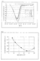
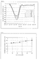
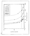
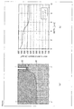
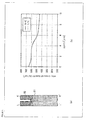
- Figs. 3 and 4 are characteristic diagrams showing the reverse recovery characteristics of the semiconductor device according to Embodiment 1.
- Fig. 3 shows reverse recovery current Iak waveforms.
- Fig. 4 shows the relationship between the anode ratio ⁇ and a reverse recovery peak current (the peak value of the reverse recovery current Iak waveform) Irp.
- the reverse recovery current Iak is calculated in cases wherein the anode ratio ⁇ of the semiconductor device according to Embodiment 1 is 12.5%, 25%, 50%, 75%, and 100%.
- the repetitive pitch of the trench 2 is taken to be 5 ⁇ m.
- the width in the lateral direction of the trench 2 is 1 ⁇ m, and the mesa width w20 between trenches 2 is 4 ⁇ m.
- the anode ratio ⁇ being 100% is a case wherein the p-type anode region 5-2 is not thinned out, that is, a case wherein the p-type anode region 5-2 is exposed over the whole of the substrate front surface in a mesa portion between neighboring trenches 2 in the FWD portion 22 (the same applies to Figs. 15 and 16 ).
- the reverse recovery peak current Irp increases in comparison with when the p-type anode region 5-2 is formed over the whole surface, that is, when the anode ratio ⁇ is 100%.
- the invention is such that, rather than an increase when the anode ratio ⁇ is 50% or more and less than 100%, there is a decrease in comparison with when the anode ratio ⁇ is 100%. This is a peculiar advantage not seen in existing diodes.
- the interval between neighboring p-type anode regions 5-2 in the trench 2 longitudinal direction is smaller than the width of a pn-junction built-in depletion layer. Therefore, built-in depletion layers spreading from each of neighboring p-type anode regions 5-2 are linked with each other in the n - -type drift region 1 sandwiched by the built-in depletion layers.
- the built-in depletion layer has reverse bias with respect to the pn-junction
- holes are not implanted into the n - -type drift region 1 to such an extent that the built-in depletion layer is extinguished, even when reverse bias is applied to the pn-junction. That is, the implantation of holes is restricted by the commonly known JFET effect. Therefore, hole implantation efficiency when the anode ratio ⁇ is 50% or more and less than 100% decreases in comparison with when the anode ratio ⁇ is 100%. Therefore, the carrier concentration distribution in a state wherein a rated current is flowing is such that there is a relative drop on the p-type anode region 5-2 side compared with the n + -type cathode region 12 side.
- the heretofore described series of actions achieves the advantage of reducing the reverse recovery peak current Irp, as shown in Figs. 3 and 4 .
- the reason for the reverse recovery peak current Irp increasing when the anode ratio ⁇ is less than 50% is that, as the built-in depletion layers spreading into the n - -type drift region 1 from the p-type anode region 5-2 on either side are not linked, the JFET effect decreases. Due to the JFET effect decreasing, accumulated carriers directly below the oxide film begin to increase, because of which the reverse recovery peak current Irp increases.
- the interval between neighboring p-type anode regions 5-2 is of, or less than, a distance such that the built-in depletion layers spreading from each p-type anode region 5-2 link with each other.
- the width Lp in the trench 2 longitudinal direction of the p-type anode region 5-2 is set to be sufficiently smaller than the mesa width w20 between trenches 2.
- the interval between neighboring p-type anode regions 5-2 can be of, or less than, a distance such that the built-in depletion layers spreading from each p-type anode region 5-2 link with each other. Therefore, the reverse recovery peak current Irp is further reduced, and the minimum value of the reverse recovery peak current Irp shown in, for example, Fig. 4 can be further reduced. Therefore, the anode ratio ⁇ at which the reverse recovery peak current Irp is at a minimum can be between 75% or more (or furthermore, 80% or more) and less than 100%.
- Figs. 5 to 8 are sectional views showing states partway through the manufacture of the semiconductor device according to Embodiment 1.
- Figs. 9 to 12 are illustrations showing states partway through the manufacture of the semiconductor device according to Embodiment 1.
- (b) shows a planar structure partway through manufacture, while (a) shows a sectional structure along a B-B' cutting line of (b).
- the resistivity of the silicon substrate is in the region of, for example, 40 ⁇ cm to 80 ⁇ cm. Therefore, the resistivity of the n - -type semiconductor substrate 31 may be in the region of, for example, 55 ⁇ cm.
- the orientation of the main surface of the silicon substrate is, for example, (100).
- a p-type guard ring for example, configuring a voltage withstanding structure is formed on the front surface side of the n - -type semiconductor substrate 31 in an edge termination structure portion omitted from the drawings.
- the edge termination structure portion is a region that relaxes an electrical field exerted on the n - -type drift region 1 in an active region, thereby maintaining breakdown voltage.
- the active region is a region in which an RC-IGBT element structure is formed.
- the edge termination structure portion is also omitted from Figs. 1, 2 , 5 to 14 , 17 , 20A to 23C , 26 , and 27 .
- a resist mask (not shown) in which is opened the formation region of the p-type guard ring is formed on the front surface of the n - -type semiconductor substrate 31.
- a p-type impurity such as, for example, boron (B) is ion implanted into the front surface of the n - -type semiconductor substrate 31.
- the p-type impurity implanted into the n - -type semiconductor substrate 31 is caused to diffuse by a thermal diffusion processing, whereby the p-type guard ring is formed.
- an oxide film 32 is formed on the front surface of the n - -type semiconductor substrate 31 by the thermal diffusion processing for forming the p-type guard ring.
- a portion of the oxide film 32 corresponding to the formation region of the trench 2 is removed by photolithography.
- anisotropic dry etching for example, is carried out, thereby forming the trench 2 to a predetermined depth in the front surface of the n - -type semiconductor substrate 31.
- a sacrificial oxide film (not shown) is formed on the inner wall of the trench 2 by sacrificial oxidation, and by the sacrificial oxide film being removed, a defect layer created on the n - -type semiconductor substrate 31 surface by the formation of the trench 2 is removed.
- the oxide film 32 covering the front surface of the n - -type semiconductor substrate 31 in the active region is removed.
- the gate insulating film 3 is formed by thermal oxidation on the front surface of the n - -type semiconductor substrate 31 so as to follow the inner wall of the trench 2.
- the thickness of the gate insulating film 3 is, for example, 100nm to 120nm, and in Embodiment 1 is, for example, 110nm.
- a conductive polycrystalline silicon film 33 is deposited on the front surface of the n - -type semiconductor substrate 31, thereby filling the interior of the trench 2.
- the conductive polycrystalline silicon film 33 is etched back until the gate insulating film 3 is exposed, leaving the conductive polycrystalline silicon film 33, which is to form the gate electrode 4, in only the interior of the trench 2.
- the gate insulating film 3 and oxide film 32 on the front surface of the n - -type semiconductor substrate 31 are removed.
- a screen oxide film 34 is formed on the front surface of the n - -type semiconductor substrate 31 using a thermal oxidation method.
- the screen oxide film 34 is omitted from Fig. 9 (b) (the same also applies to (b) in Figs. 10 to 12 ).
- a resist mask 35 having a first aperture portion 35a that exposes the formation region of the p-type base region 5-1 and a second aperture portion 35b that exposes the formation region of the p-type anode region 5-2 is formed by photolithography on the front surface of the n - -type semiconductor substrate 31.
- the width Lp in the trench 2 longitudinal direction of the second aperture portion 35b of the resist mask 35 is set so that the anode ratio ⁇ expressed in Expression (1) is within a range of 50% to 75%.
- a first ion implantation 41 of a p-type impurity such as, for example, boron is carried out through the screen oxide film 34 into the front surface of the n - -type semiconductor substrate 31.
- P-type impurity regions 5-1a and 5-2a are formed by the first ion implantation 41 in the n - -type drift region 1 exposed in the first and second aperture portions 35a and 35b of the resist mask 35.
- the resist mask 35 is removed.
- the p-type base region 5-1 of the IGBT portion 21 and p-type anode region 5-2 of the FWD portion 22 are to be formed to have differing impurity concentrations, it is sufficient to form a further resist mask and carry out a further p-type impurity ion implantation.
- a resist mask in which only the formation region of the p-type base region 5-1 in the region of the IGBT portion 21 is selectively opened is formed first.
- an ion implantation of, for example, boron is carried out at a dose of in the region of 2 ⁇ 10 13 /cm 2 and an acceleration energy of in the region of 100keV, after which the resist mask is removed.
- a resist mask in which only the formation region of the p-type anode region 5-2 in the region of the FWD portion 22 is selectively opened is formed.
- an ion implantation of, for example, boron is carried out at a dose within a range of in the region of 1 ⁇ 10 12 /cm 2 or more, 1 ⁇ 10 13 /cm 2 or less, and at an acceleration energy of in the region of 100keV, after which the resist mask is removed.
- a thermal diffusion processing is carried out at a temperature within a range of in the region of 1,050°C or more, 1,150°C or less, thereby forming the p-type base region 5-1, formed by the p-type impurity region 5-1a being thermally diffused, and the p-type anode region 5-2, formed by the p-type impurity region 5-2a being thermally diffused.
- the gate threshold of the semiconductor device is approximately 6V.
- a resist mask 36 having an aperture portion that exposes the formation region of the p + -type contact region 7 is formed by photolithography on the front surface of the n - -type semiconductor substrate 31.
- the aperture portion of the resist mask 36 is in only the region of the IGBT portion 21, and is not formed in the FWD portion 22.
- a second ion implantation 42 of a p-type impurity such as, for example, boron is carried out through the screen oxide film 34 into the front surface of the n - -type semiconductor substrate 31.
- the dose of the ion implantation may be within a range of in the region of, for example, 1 ⁇ 10 15 /cm 2 or more, 5 ⁇ 10 15 /cm 2 or less, and the acceleration energy may be in the region of 100keV.
- the p + -type contact region 7 is formed inside the p-type base region 5-1, only in the IGBT portion 21, by thermally diffusing the p-type impurity implanted by the second ion implantation 42 at a temperature in the region of, for example, 1,000°C.
- the resist mask 36 is omitted from Fig. 11(b) .
- a resist mask 37 having an aperture portion that exposes the formation region of the n + -type emitter region 6 is formed by photolithography on the front surface of the n - -type semiconductor substrate 31.
- a third ion implantation 43 of an n-type impurity such as, for example, arsenic (As) is carried out through the screen oxide film 34 into the front surface of the n - -type semiconductor substrate 31.
- the n + -type emitter region 6 is formed inside the p-type base region 5-1 by thermally diffusing the n-type impurity implanted by the third ion implantation 43.
- the resist mask 37 is omitted from Fig. 12(b) .
- the interlayer dielectric 8, of BPSG (borophosphosilicate glass) or the like, is formed over the whole of the front surface of the n - -type semiconductor substrate 31.
- the interlayer dielectric 8 is selectively removed by photolithography, thereby forming the first and second contact holes 8-1 and 8-2.
- the emitter electrode 9 is formed on the front surface of the n - -type semiconductor substrate 31 using a general method, the front surface of the n - -type semiconductor substrate 31 is protected with, for example, a resist film (not shown).
- a grinding strain layer is removed by etching.
- a fourth ion implantation of an n-type impurity such as, for example, selenium (Se) is carried out from the back surface of the n - -type semiconductor substrate 31.
- the fourth ion implantation is an ion implantation for forming the n-type buffer layer 10, and may be carried out at, for example, a dose of in the region of 3 ⁇ 10 14 /cm 2 and an acceleration energy of in the region of 100keV.
- a fifth ion implantation of a p-type impurity such as, for example, boron is carried out from the back surface of the n - -type semiconductor substrate 31 into a region shallower than the fourth ion implantation.
- the fifth ion implantation is an ion implantation for forming the p + -type collector region 11, and may be carried out at, for example, a dose of in the region of 8 ⁇ 10 13 /cm 2 and an acceleration energy of in the region of 40keV.
- a resist mask (not shown) of a thickness in the region of, for example, 2 ⁇ m and having an aperture portion that exposes the formation region of the n + -type cathode region 12, that is, the FWD portion 22, is formed by photolithography on the back surface of the n - -type semiconductor substrate 31.
- a sixth ion implantation of an n-type impurity such as, for example, phosphorus (P) is carried out into the back surface of the n - -type semiconductor substrate 31.
- the sixth ion implantation may be carried out at, for example, a dose of in the region of 2 ⁇ 10 15 /cm 2 and an acceleration energy of in the region of 110keV.
- the resist mask protecting the front surface of the n - -type semiconductor substrate 31 and the resist mask on the back surface of the n - -type semiconductor substrate 31 are removed.
- the impurity regions formed by the fourth to sixth ion implantations are activated by carrying out a thermal processing for in the region of 30 minutes at a temperature in the region of, for example, 950°C.
- an aluminum-silicon (Al-Si, for example, Al including 1% Si) film of a thickness in the region of, for example, 5 ⁇ m is formed on the front surface side of the n - -type semiconductor substrate 31.
- the emitter electrode 9 is formed by patterning the Al-Si film.
- an irradiation with, for example, helium (4He) is carried out from the back surface of the n - -type semiconductor substrate 31 at an acceleration energy of in the region of 23MeV and a dose of in the region of 1 ⁇ 10 13 /cm 2 .
- an annealing is carried out for in the region of one hour at a temperature in the region of 370°C, thereby causing recovery of defects occurring inside the n - -type semiconductor substrate 31 due to the helium irradiation.
- the collector electrode 13 is formed by an Al film, Ti film, Ni film, and gold (Au) film being deposited sequentially to thicknesses of in the region of 1 ⁇ m, 0.07 ⁇ m, 1 ⁇ m, and 0.3 ⁇ m respectively on the back surface of the n - -type semiconductor substrate 31, thereby completing the RC-IGBT shown in Figs. 1 and 2 .
- Embodiment 1 reverse recovery current can be reduced, and reverse recovery loss can thereby be reduced, by adopting an anode ratio of 50% to 75%, because of which the diode characteristics can be improved. Also, according to Embodiment 1, no Schottky junction of the emitter electrode and n - -type drift region is formed in the FWD portion, because of which leakage current can be prevented from increasing when in an off-state. Also, according to Embodiment 1, the region in which only the IGBT is provided (the IGBT portion) can be secured over a greater area than in PTL 2 by the IGBT portion and FWD portion being disposed separately. Therefore, even when carriers are extracted from the FWD portion, the carrier concentration in the IGBT portion can be maintained at a high level. Therefore, the on-state resistance can be reduced, and the on-state voltage can thereby be reduced.
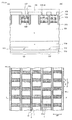
- Fig. 13 is a plan view showing the structure of the semiconductor device according to Embodiment 2.
- Fig. 14 is a sectional view showing the sectional structure along a cutting line C-C' of Fig. 13 .
- the semiconductor device according to Embodiment 2 differs from the semiconductor device according to Embodiment 1 in the following two ways. The first difference is that practically the whole of a mesa portion between neighboring trenches 2 in the FWD portion 22 is exposed in a second contact hole 58-2, and both the p-type anode region 5-2 and n - -type drift region 1 are connected to the emitter electrode 9.
- a Schottky junction of the n - -type drift region 1 and emitter electrode 9 is formed in the FWD portion 22.
- a material such as, for example, Al including 1% Si, platinum (Pt), or platinum silicide (PtSi), wherein a height ⁇ B of a Schottky barrier at an interface with a silicon portion is 0.8eV or more, is used as the material configuring at least the portion of the emitter electrode 9 in contact with the silicon portion of the FWD portion 22.
- the second difference is that the lower the anode ratio ⁇ the better ( ⁇ ⁇ 0%), and it is good when the anode ratio ⁇ is, for example, less than 50%, preferably 25% or less.
- the reason for this is that the lower the anode ratio ⁇ , the farther the recovery peak current Irp can be reduced.
- Figs. 15 and 16 are characteristic diagrams showing the reverse recovery characteristics of the semiconductor device according to Embodiment 2. Fig. 15 shows the reverse recovery current Iak waveforms. Fig. 16 shows the relationship between the anode ratio ⁇ and the reverse recovery peak current Irp.
- the reverse recovery current Iak is calculated in cases wherein the anode ratio ⁇ of the semiconductor device according to Embodiment 2 is 15%, 25%, 50%, 75%, and 100%.
- the width (not including an increase caused by thermal diffusion) Lp in the trench 2 longitudinal direction of the p-type anode region 5-2 is taken to be 5 ⁇ m.
- the anode ratio ⁇ is changed, and the reverse recovery current Iak calculated.
- the method of manufacturing the semiconductor device according to Embodiment 2 is the same as the method of manufacturing the semiconductor device according to Embodiment 1.
- Fig. 24 is a characteristic diagram showing the relationship between the width of the IGBT portion and the width of the FWD portion in the semiconductor device according to Embodiment 2.
- Fig. 25 is a plan view showing the planar configuration of the semiconductor device in Embodiment 2. As shown in Fig. 25 , an edge termination region 72 is formed so as to enclose the active region in an outer peripheral portion of the chip of the reverse conducting IGBT formed of the IGBT portion 21 and FWD portion 22. A gate runner 73 is formed along an outer peripheral portion of the active region and so as to be enclosed by the edge termination region 72.
- the gate runner 73 is a wire for supplying a gate signal from a gate pad 74 to the IGBT cell inside the active region.
- the IGBT portion 21 and FWD portion 22, of predetermined sizes, are repeatedly, alternately disposed in a region (a region on the inner side of the active region) surrounded by the gate runner 73.
- a width W IGBT of the IGBT portion 21 is taken to be the length between neighboring FWD portions 22 in the direction in which the IGBT portion 21 and FWD portion 22 are repeatedly, alternately disposed. That is, the shorter width of the IGBT portion 21, which has, for example, an approximately rectangular planar form, is taken to be W IGBT .
- a width W FWD of the FWD portion 22 is taken to be the length between neighboring IGBT portions 21 in the direction in which the IGBT portion 21 and FWD portion 22 are repeatedly, alternately disposed. That is, the shorter width of the FWD portion 22, which has, for example, an approximately rectangular planar form, is taken to be W FWD .
- Fig. 24 shows a graph showing on-state voltage when the current density is 400A/cm 2 and the temperature is 125°C.
- Fig. 24 shows the on-state voltage when the width W FWD of the FWD portion 22 is 1 ⁇ m, 3 ⁇ m, 10 ⁇ m, 100 ⁇ m, and 1, 000 ⁇ m by approximate curves linking a multiple of data points.
- the vertical axis is on-state voltage
- the horizontal axis is the IGBT portion width W IGBT .
- the on-state voltage when the whole of the region surrounded by the gate runner 73 is the IGBT portion (that is, the FWD portion is not provided) is 1.1V
- the position of on-state voltage 1.1V is indicated by the thickest broken line (horizontal line) in Fig. 24 .
- the on-state voltage increases on the width W IGBT of the IGBT portion 21 becoming less than a certain width at each width W FWD of the FWD portion 22.
- the on-state voltage increases sharply in response to a reduction in the width W IGBT of the IGBT portion 21 when the on-state voltage is 1.3V or higher.
- the on-state voltage being 1. 3V corresponds to snapback occurring without current increasing in the current-voltage curve.
- Snapback is a phenomenon whereby electrons implanted from the MOS gate of the IGBT portion 21 pass through the field stop layer (n-type buffer layer 10) and flow into the n + -type cathode region 12 of the FWD portion 22 neighboring the IGBT portion 21, because of which hole implantation from the p + -type collector region 11 of the IGBT portion 21 is impeded.
- the width W IGBT of the IGBT portion 21 is a width such that the on-state voltage is lower than 1.3V.
- the width W FWD of the FWD portion 22 is at least 1 ⁇ m, because of which it is good when the width W IGBT of the IGBT portion 21 is 20 ⁇ m or greater.
- width W FWD of the FWD portion 22 taking the width W FWD of the FWD portion 22 to be 10 ⁇ m, increase in the on-state voltage can be restricted provided that the width W IGBT of the IGBT portion 21 is 20 ⁇ m or greater. Also, it is necessary that when the width W FWD of the FWD portion 22 is, for example, 100 ⁇ m, the width W IGBT of the IGBT portion 21 is 100 ⁇ m or greater, and when the width W FWD of the FWD portion 22 is, for example, 1,000 ⁇ m, the width W IGBT of the IGBT portion 21 is 1,000 ⁇ m or greater.
- the width W IGBT of the IGBT portion 21 is 300 ⁇ m or less, in which case it is preferable that the width W FWD of the FWD portion 22, although also depending on the current density ratio, is 150 ⁇ m or less. According to the above, it is preferable that the width W IGBT of the IGBT portion 21 is 20 ⁇ m or more, 300 ⁇ m or less, and that the width W FWD of the FWD portion 22 is 10 ⁇ m or more, 150 ⁇ m or less.
- the width W IGBT of the IGBT portion 21 being 20 ⁇ m or more, 100 ⁇ m or less
- the width W FWD of the FWD portion 22 being 10 ⁇ m or more, 50 ⁇ m or less
- the mesa width w20 between trenches 2 may be further reduced beyond 4 ⁇ m.
- a built-in depletion layer is spreading in the mesa portion from the boundary between the trench 2 and mesa portion.
- the repetitive pitch in the trench 2 longitudinal direction of the p-type anode region 5-2 may be ten times or more greater than the mesa width w20 between trenches 2.
- the trench 2 of the FWD portion 22 may be provided at differing trench intervals.
- Fig. 26 is a plan view showing another example of the semiconductor device according to Embodiment 2.
- Fig. 27 is a sectional view showing the sectional structure along a cutting line H-H' of Fig. 26 .
- the trench 2 of the FWD portion 22 may be disposed at, for example, a first trench interval La and a second trench interval Lb wider than the first trench interval La.
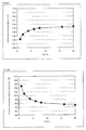
- Fig. 28 is a characteristic diagram showing the relationship between the trench interval ratio Lb/La and reverse recovery current I AK of the semiconductor device of Fig. 26 .
- the reverse recovery peak current Irp decreases in comparison with when the first trench interval La and second trench interval Lb are equal.
- Fig. 29A is a characteristic diagram showing the relationship between the trench interval ratio Lb/La and forward voltage drop Vf of the semiconductor device of Fig. 26 .
- Fig.29B is a characteristic diagram showing the relationship between the trench interval ratio Lb/La and reverse recovery peak current Irp of the semiconductor device of Fig. 26 .
- Fig. 30A(b) shows the current density distribution in sections cut along cutting lines I-I' and J-J' of Fig. 30A(a) .
- FIG. 30B (b) shows the current density distribution in sections cut along cutting lines K-K' and L-L' of Fig. 30B(a) .
- Figs. 30A(a) and 30B(a) only one trench 82 is shown, and trenches 82 neighboring this trench 82 on either side in the lateral direction are omitted, but a region of a semiconductor substrate 81 to the right of the trench 82 is a region sandwiched by trenches 82 neighboring at the first trench interval La, while a region to the left of the trench 82 is a region sandwiched by trenches 82 neighboring at the second trench interval Lb.
- Figs. 30A(a) and 30B(a) only one trench 82 is shown, and trenches 82 neighboring this trench 82 on either side in the lateral direction are omitted, but a region of a semiconductor substrate 81 to the right of the trench 82 is a region sandwiched by trenches 82 neighboring at the first trench interval La
- the vertical axis is the hole current density
- the differing hatchings shown inside the semiconductor substrate 81 indicate high and low hole current densities, and as shown in Figs. 30A(b) and 30B(b) , the hole current density inside the semiconductor substrate 81 becomes lower the greater the depth from the front surface of the semiconductor substrate 81. Also, the hole current density inside the semiconductor substrate 81 becomes lower the farther from the trench 82 in the lateral direction of the trench 82.
- the pitch La + Lb 8
- the current density of the narrow region of the semiconductor substrate 81 sandwiched by trenches 82 neighboring at the first trench interval La is higher than the current density of another region.
- the pitch La + Lb being large is the reason the increase in the forward voltage drop Vf is suppressed to in the region of 2%.
- the reverse recovery current I AK operation in the narrow region of the semiconductor substrate 81 sandwiched by trenches 82 neighboring at the first trench interval La becomes a main operation by the anode region (not shown) being partitioned (divided) into multiple portions by the trench 82, because of which the implantation efficiency decreases. Therefore, discharge of holes when there is a reverse recovery operation is facilitated, and the reverse recovery peak current Irp decreases.
- the trench interval ratio Lb/La is greater than 1 (1 ⁇ Lb/La), and preferably 2 or greater (2 ⁇ Lb/La). Also, as the characteristics are practically saturated when the trench interval ratio Lb/La is 10 or greater, it is good when the trench interval ratio Lb/La is 10 or less (Lb/La ⁇ 10), and preferably, it is good when the trench interval ratio Lb/La is 5 or less (Lb/La ⁇ 5), which can reduce the forward voltage.
- the trench interval ratio Lb/La may be 10 or greater, but as current is liable to concentrate in a narrow region sandwiched by trenches 82 neighboring at the first trench interval La, it is preferable in terms of preventing current concentration too that the trench interval ratio Lb/La is 10 or less.
- the reverse recovery peak current can be further reduced by a Schottky junction of the n - -type drift region and emitter electrode being formed in the FWD portion.
- a depletion layer extending from the pn-junction between the p-type anode region and n - -type drift region, and from the boundary between the trench and n - -type drift region, is easily pinched off, because of which leakage current can be prevented from increasing when in an off-state.
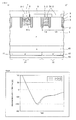
- Fig. 17 is a sectional view showing the structure of the semiconductor device according to Embodiment 3.
- the semiconductor device according to Embodiment 3 differs from the semiconductor device according to Embodiment 2 in that a gate electrode 54 in the FWD portion 22 and the emitter electrode 9 are conductively connected. That is, the gate electrode 54 of the FWD portion 22 is of the emitter potential.
- the gate electrode 4 of the IGBT portion 21 is electrically isolated from the gate electrode 54 of the FWD portion 22 in a portion omitted from the drawing.
- Embodiment 3 As heretofore described, according to Embodiment 3, the same advantages as in Embodiments 1 and 2 can be obtained.
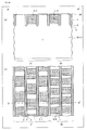
- Fig. 20A is a plan view showing the structure of the semiconductor device according to Embodiment 4.
- Fig. 20B is a plan view showing the structure of another example of the semiconductor device according to Embodiment 4.
- Fig. 21 is a sectional view showing the sectional structure along a cutting line D-D' of Figs. 20A and 20B .
- the semiconductor device according to Embodiment 4 being only the FWD portion in Embodiment 3, is a diode of a configuration wherein built-in depletion layers spreading in a mesa portion from trenches 2 on either side are linked. Configurations other than this of the semiconductor device according to Embodiment 4 are the same as in Embodiment 3.
- Reference sign 59 is an anode electrode, while reference sign 63 is a cathode electrode.
- the resistivity of an n - -type silicon substrate that is to form the n - -type drift region 1 is typically 30 ⁇ cm to 325 ⁇ cm, wherein the unit of a value that is 0.05 times the rated voltage is converted. Therefore, the width of a built-in depletion layer spreading in the mesa portion from the trench 2 on one side, using Poisson's equation, is approximately 2.4 ⁇ m to 7.8 ⁇ m.
- the mesa width w20 between trenches 2 is less than 4.8 ⁇ m to 15.6 ⁇ m when the rated voltage is 600V to 6,500V, the built-in depletion layers spreading from the trench 2 on either side of the mesa portion link up. More preferably, by further reducing the mesa width w20 between trenches 2 so as to be, for example, 2.4 ⁇ m to 7.8 ⁇ m or less, half of the previously mentioned values, when the rated voltage is 600V to 6,500V, an increase in leakage current due to the mirror image effect can be still more reliably suppressed.
- Expression (2) defines the resistivity of a typical semiconductor substrate with respect to the rated voltage V using the heretofore described method, and is such that the built-in depletion layer width is obtained in accordance with Poisson's equation at seven points of the rated voltage V between 600V and 6,500V (600V, 1,200V, 1,700V, 2,500V, 3,300V, 4,500V, and 6,500V), and the values fitted with a sextic polynomial expression.
- the mesa width w20 between trenches 2 When reducing the mesa width w20 between trenches 2, it is sufficient that the mesa width w20 is smaller than the value of the mesa width w20 calculated using Expression (2), for example, it is sufficient that the mesa width w20 between trenches 2 is one-half of the value of the mesa width w20 calculated using Expression (2).
- the p-type anode region 5-2 may be disposed so as to oppose a region (the n - -type drift region 1) between two p-type anode regions 5-2 neighboring across the trench 2. As holes are implanted from the p-type anode region 5-2, the current density of a portion below the p-type anode region 5-2 increases.
- the p-type anode region 5-2 is disposed as in Fig. 20B , p-type anode regions 5-2 neighboring across the trench 2 are distanced from each other, because of which regions with high current density are dispersed, and heat generation, current crowding, and the like, can be restricted.
- a diode wherein increase in leakage current is suppressed can be obtained by sufficiently reducing the mesa width between trenches, even when there is no p-type anode region.
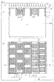
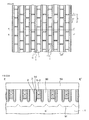
- Fig. 22A is a plan view showing the structure of the semiconductor device according to Embodiment 5.
- Fig. 22B is a sectional view showing the sectional structure along a cutting line E-E' of Fig. 22A .
- Fig. 22C is a sectional view showing the sectional structure along a cutting line F-F' of Fig. 22A .
- the semiconductor device according to Embodiment 5 differs from the semiconductor device according to Embodiment 4 in the following two ways. The first difference is that the p-type anode region 5-2 is selectively formed in the trench 2 longitudinal direction so that the anode ratio ⁇ is 10% or less.
- the second difference is that the repetitive pitch of the trench 2 is sufficiently smaller than the built-in depletion layer width, for example, the mesa width w20 between trenches 2 is one-half or less of the value of Expression (2), and equal to or greater than the width in the lateral direction of the trench 2.
- Figs. 22B and 22C show aspects of a built-in depletion layer 90 spreading.
- the built-in depletion layer 90 is a depletion layer that spreads into the n - -type drift region 1 from the pn-junction between the p-type anode region 5-2 and n - -type drift region 1 in a state of thermal equilibrium, with no voltage being applied to the anode electrode 59 or a cathode electrode (not shown).
- the mesa width w20 between trenches 2 is one-half or less of the value of Expression (2)
- built-in depletion layers 90 spreading into the mesa portion from neighboring trenches 2 are connected with each other, as shown in Fig. 22B .
- a depletion layer end 91 of the built-in depletion layer 90 is at a depth equivalent to the depth of the p-type anode region 5-2, and the surface form of the depletion layer end 91 of the built-in depletion layer 90 is in a practically flat state parallel to the substrate main surface. Therefore, the depletion layer end 91 of the built-in depletion layer 90 is of a form near that of a planar junction, and breakdown voltage increases.
- a planar junction is a pn-junction between the p-type anode region 5-2 and n - -type drift region 1 when the p-type anode region 5-2 is provided uniformly in a surface layer of the front surface of the n - -type semiconductor substrate.
- the depletion layer end 91 of the built-in depletion layer 90 being of a form near that of a planar junction, a decrease in the barrier height at a Schottky contact can also be restricted, because of which there is almost no increase in leakage current even when a high voltage is applied. Furthermore, even when the second pitch in the trench 2 longitudinal direction of the p-type anode region 5-2 is sufficiently longer than the width of the built-in depletion layer 90, and the anode ratio ⁇ is 10% or less, neither breakdown voltage nor leakage current depends on the second pitch in the trench 2 longitudinal direction of the p-type anode region 5-2.
- the surface form of the depletion layer end 91 of the built-in depletion layer 90 is sufficiently near that of a planar junction even in a region in which the p-type anode region 5-2 is not provided on the cutting line.
- This kind of structure is such that the hole implantation efficiency of the anode electrode 59 can be dramatically reduced (to 10% or less) by the anode ratio ⁇ being 10% or less, because of which reverse recovery current can be reduced without causing a decrease in breakdown voltage or an increase in leakage current.
- Embodiment 5 As heretofore described, according to Embodiment 5, the same advantages as in Embodiments 3 and 4 can be obtained.
- Fig. 23A is a plan view showing the structure of the semiconductor device according to Embodiment 6.
- Fig. 23B is a sectional view showing the sectional structure along a cutting line G-G' of Fig. 23A .
- Fig. 23C is a sectional view showing another example of the sectional structure along the cutting line G-G' of Fig. 23A .
- the semiconductor device according to Embodiment 6 differs from the semiconductor device according to Embodiment 5 in that there is only a Schottky contact of the n - -type drift region 1 and anode electrode 59, as shown in Fig. 23B , with no p-type anode region being formed.
- the surface form of the depletion layer end 91 of the built-in depletion layer 90 is sufficiently near that of a planar junction, even when there is no p-type anode region 5-2, owing to the repetitive pitch of the trench 2 being sufficiently small. Further, by not forming the p-type anode region 5-2, the hole implantation efficiency from the p-type anode region 5-2 into the n - -type drift region 1 can be reduced to practically 0 (zero) without causing a decrease in breakdown voltage or an increase in leakage current.
- anode electrode 59 When forming the anode electrode 59 using an aluminum-silicon (Al-Si) alloy, platinum silicide (PtSi), or the like, which have a high Schottky barrier, hole implantation from the p-type anode region 5-2 into the n - -type drift region 1 occurs, because of which the hole implantation efficiency cannot be reduced to zero, but the hole implantation efficiency can be reduced to one-half or less compared with that when forming the p-type anode region 5-2.
- Al-Si aluminum-silicon
- PtSi platinum silicide
- a shallow p-type layer 5-3 sufficiently shallower than the p-type anode region 5-2 of Embodiment 5 and of a low impurity concentration, may be formed as a modification example of Embodiment 6.
- a depletion layer spreads with respect to surface defects (surface level) introduced partway through the element formation process, and carrier generation due to thermal excitation is liable to occur. Therefore, there is concern that leakage current will increase, and yield decrease. Therefore, by the shallow p-type layer 5-3 being formed as in the modification example of Embodiment 6 of Fig. 23C , the depletion layer can be prevented from coming into contact with the surface defects (surface level), because of which leakage current is stable at a low value, and yield decrease can be restricted.
- Embodiments 4 to 6 may also be applied to the FWD portion 22 of the semiconductor device in Embodiment 2. Also, the shallow p-type layer 5-3 in the modification example of Embodiment 6 may be formed in Embodiments 4 and 5. By so doing, the same advantages as in
- Embodiment 6 can be achieved.
- Embodiment 6 As heretofore described, according to Embodiment 6, the same advantages as in Embodiments 3 to 5 can be obtained.
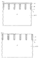
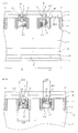
- Fig. 31 is a sectional view showing the structure of the semiconductor device according to Embodiment 7.
- the planar structure of the semiconductor device according to Embodiment 7 shown in Fig. 31 being the same as that of Fig. 1
- Fig. 31 is the sectional structure along the cutting line A-A' of Fig. 1
- Fig. 32 is a sectional view showing the structure of another example of the semiconductor device according to Embodiment 7.
- the planar structure of the other example of the semiconductor device according to Embodiment 7 shown in Fig. 32 being the same as that of Fig. 13
- Fig. 32 is the sectional structure along the cutting line C-C' of Fig. 13 .
- Fig. 33 is a sectional view showing the structure of a semiconductor device of a comparison example.
- the semiconductor device according to Embodiment 7 differs from the semiconductor device according to Embodiment 1 in that the p-type base region 5-1 and p-type anode region 5-2 are each electrically connected to the emitter electrode 9 via a contact electrode 18.
- the contact electrode 18 is formed by a titanium (Ti) layer 14, titanium nitride (TiN) layer 15, and tungsten (W) layer 16 being deposited sequentially from the front surface side of the substrate.
- a p + -type contact region 17 is selectively provided inside the p-type anode region 5-2.
- the p + -type contact region 17 realizes ohmic contact (ohmic electrical contact) to the titanium layer 14.
- the p + -type contact region 17 has a depth and impurity concentration differing from those of the p + -type contact region 7 of the IGBT portion 21, and is adjusted (optimized) so that predetermined FWD characteristics based on design conditions are obtained.
- the depth of the p + -type contact region 17 is less than the depth of the p + -type contact region 7, and that the impurity concentration of the p + -type contact region 17 is lower than the impurity concentration of the p + -type contact region 7.
- the reason for this is that when the p + -type contact region 17 is formed in the p-type anode region 5-2 to a depth of the same extent as that of the p + -type contact region 7 of the IGBT portion 21, and with a high impurity concentration, hole implantation from the p-type anode region 5-2 into the n - -type drift region 1 increases too far when the FWD is in an on-state, and hard recovery occurs.
- the contact electrode 18 is embedded inside each of, for example, the first and second contact holes 8-1 and 8-2.
- the contact electrode 18 realizes good ohmic contact, even when an aperture width w31 in the trench 2 lateral direction of the first contact hole 8-1 and the aperture width w21 in the trench 2 lateral direction of the second contact hole 8-2 are small due to a repetitive pitch L30 of the trench 2 being small at, for example, 4 ⁇ m or less.
- the contact electrode 18 is not included, as in the comparison example shown in Fig. 33 , the aperture width w31 in the trench 2 lateral direction of the first contact hole 8-1 and the aperture width w21 in the trench 2 lateral direction of the second contact hole 8-2 are small due to the repetitive pitch L30 of the trench 2 being small.
- the interiors of the first and second contact holes 8-1 and 8-2 cannot be completely filled by only the emitter electrode 9, which is formed of an aluminum-silicon film. Therefore, a gap 19 occurs between the emitter electrode 9 and the silicon portion (at least the p + -type contact region 7 of the IGBT portion 21, and the p-type anode region 5-2 of the FWD portion 22), and contact resistance increases, because of which it is difficult to obtain good ohmic contact between the emitter electrode 9 and silicon portion.
- the invention is such that the interiors of the first and second contact holes 8-1 and 8-2 can be completely filled by the contact electrode 18 formed of the titanium layer 14, titanium nitride layer 15, and tungsten layer 16. Therefore, the gap 19 can be prevented from occurring between the emitter electrode 9 and silicon portion.
- the titanium layer 14 is provided along the side walls and substrate front surface inside each of the first and second contact holes 8-1 and 8-2. The titanium layer 14 is in contact with the n + -type emitter region 6 and p + -type contact region 7 in the IGBT portion 21, and in contact with the p-type anode region 5-2 and p + -type contact region 17 in the FWD portion 22.
- the titanium nitride layer 15 is provided along the titanium layer 14, on the inner side of the titanium layer 14, inside the first and second contact holes 8-1 and 8-2, and the tungsten layer 16 is provided on the inner side of the titanium nitride layer 15.
- the emitter electrode 9 is in contact with the titanium layer 14, titanium nitride layer 15, and tungsten layer 16.
- the gate electrode 4 in the FWD portion 22 is of the gate potential
- the forward voltage when gate voltage is applied rises considerably.
- the rate of rise of the forward voltage is in the region of 3% when the repetitive pitch L30 of the trench 2 is 5 ⁇ m
- the region of 21% when the repetitive pitch L30 of the trench 2 is 2. 3 ⁇ m.
- the rate of rise of the forward voltage increases in proportion to the size of the gate voltage.
- the reason for this is as follows.
- gate voltage When gate voltage is applied, electrons concentrate in the periphery of the trench 2, because of which hole implantation from the p-type anode region 5-2 into the n - -type drift region 1 is restricted by the electrons concentrated in the periphery of the trench 2 in the FWD portion 22.
- the gate electrode 4 in the FWD portion 22 and the emitter electrode 9 may be conductively connected. Owing to the gate electrode 4 in the FWD portion 22 and the emitter electrode 9 being conductively connected, electrons do not concentrate in the periphery of the trench 2 in the FWD portion 22 when gate voltage is applied. Therefore, even when the repetitive pitch L30 of the trench 2 is miniaturized, hole implantation from the p-type anode region 5-2 into the n - -type drift region 1 is not restricted by electrons, because of which the forward voltage can be reduced. Also, as shown in Fig. 32 , Embodiment 7 may be applied to Embodiment 2.
- the p + -type contact region 17 may be provided inside the p-type anode region 5-2, and the emitter electrode 9 and p + -type contact region 17 connected via the contact electrode 18. In this way, good ohmic contact to the silicon portion can be realized by the contact electrode 18, regardless of the planar form of the second contact hole 58-2.
- Embodiment 7 As heretofore described, according to Embodiment 7, the same advantages as in Embodiments 1 and 2 can be obtained. According to Embodiment 7, even when attempting a reduction in on-state voltage by reducing the repetitive pitch of the trench to, for example, 4 ⁇ m or less, a rise in the forward voltage when gate voltage is applied can be restricted, and good ohmic contact can be realized on the anode side of the FWD portion.
- each portion in each of the heretofore described embodiments are variously set in accordance with the required specifications or the like.
- a first conductivity type is taken to be n-type and a second conductivity type is taken to be p-type, but the invention is established in the same way when the first conductivity type is p-type and the second conductivity type is n-type.
- the semiconductor device according to the invention is useful in a power semiconductor device used in a power conversion device or the like.
Landscapes
- Metal-Oxide And Bipolar Metal-Oxide Semiconductor Integrated Circuits (AREA)
Abstract
Description
- The present invention relates to a semiconductor device.
- In response to demand for a reduction in size and an increase in performance in power supply instruments in the field of power electronics in recent years, efforts have been focused on improving performance with respect to increasing breakdown voltage, increasing current, reducing loss, increasing breakdown resistance, and increasing speed in power semiconductors. A MOS power device driven by a MOS gate (an insulated gate formed of metal-oxide-semiconductor) is commonly known as a power semiconductor device wherein increasing current and reducing loss are possible.
- Two kinds of structure are widely known as MOS gate structures of the MOS power device, those being a planar gate structure, wherein a MOS gate is provided in plate form on a semiconductor substrate, and a trench gate structure, wherein a MOS gate is embedded in a trench formed in a semiconductor substrate. The trench gate structure is attracting attention in recent vertical power devices, as the structure thereof is such that low on-state resistance characteristics are easily obtained.
- A device wherein the surfaces of a p-type channel region and an n-type semiconductor substrate are disposed so as to appear alternately in a longitudinal direction between parallel trenches, and the surface form of an n+-type emitter region selectively formed in a surface layer of the p-type channel region is wider on the trench side and becomes narrower toward the center between trenches, has been proposed as a vertical MOS power device with this trench gate structure (for example, refer to PTL 1).
- Also, as another vertical MOS power device, there have also been advancements in the development of a reverse conducting IGBT (RC-IGBT) of a structure wherein an insulated gate bipolar transistor (IGBT) and a freewheeling diode (FWD) connected in anti-parallel to the IGBT are integrated by being incorporated in the same semiconductor substrate (semiconductor chip), in order to achieve a reduction in size of a whole power conversion device.
- A description will be given of an existing RC-IGBT.
Fig. 18 is a plan view showing the structure of the existing RC-IGBT.Fig. 19 is a sectional view showing the sectional structure along a cutting line AA-AA' ofFig. 18 . As shown inFigs. 18 and19 , the existing RC-IGBT includes a general field stop IGBT (FS-IGBT) and an FWD connected in anti-parallel to the FS-IGBT on the same n--type semiconductor substrate, which forms an n--type drift region 101. - Normally, in order to connect an FWD in anti-parallel to an FS-IGBT, an RC-IGBT has a structure wherein, taking a p-type base region configuring a MOS gate structure on the front surface side of an n--type semiconductor substrate to be a p-type anode region 105-2, one portion of a p+-
type collector region 111 provided on the back surface side of the n--type semiconductor substrate is replaced with an n+-type cathode region 112. Specifically, anIGBT portion 121 in which an FS-IGBT is provided and anFWD portion 122 in which an FWD is provided are provided on the same n--type semiconductor substrate. - A trench gate type MOS gate structure formed of a
trench 102,gate insulating film 103,gate electrode 104, p-type base region 105-1, n+-type emitter region 106, and p+-type contact region 107, and anemitter electrode 109, are provided on the front surface side of the n--type semiconductor substrate in theIGBT portion 121. The p-type base region 105-1 is disposed at predetermined intervals in the longitudinal direction of thetrench 102 in a mesa portion (a region sandwiched between neighboring trenches 102) between neighboringtrenches 102. - The trench gate formed of the
trench 102, gateinsulating film 103, andgate electrode 104 is provided in a stripe form extending in a direction (the longitudinal direction) perpendicular to the direction in which theIGBT portion 121 andFWB portion 122 are aligned (the lateral direction) from theIGBT portion 121 across theFWB portion 122. The p-type anode region 105-2 is provided over the whole of the front surface of the n--type semiconductor substrate in a mesa portion between neighboringtrenches 102 in the FWDportion 122. - The p-type anode region 105-2 is conductively connected to the
emitter electrode 109. On the back surface side of the n--type semiconductor substrate, the p+-type collector region 111 is provided in theIGBT portion 121 and the n+-type cathode region 112 is provided in the FWDportion 122. An n-type buffer layer 110 is provided between the p+-type collector region 111 and n+-type cathode region 112 and the n--type drift region 101. Acollector electrode 113 is in contact with the p+-type collector region 111 and n+-type cathode region 112.Reference sign 108 is an interlayer dielectric. - A collector short device wherein a MOS gate structure is repeatedly disposed in a pattern the same as that of a normal IGBT on the front surface of a semiconductor chip, and an FWD portion n+-type cathode region and IGBT portion p+-type collector region are disposed in parallel on the back surface of the semiconductor chip, has been proposed as this kind of RC-IGBT (for example, refer to PTL 2).
- Also, a device wherein an IGBT portion acting as an IGBT element and a diode region acting as a diode element are repeatedly, alternately disposed on a semiconductor substrate including an n--type drift layer, and a p-type Schottky contact region that extracts holes from the ri -type drift layer is provided in a surface layer portion of the n--type drift layer in a portion of the diode region farthest to the IGBT portion side, has been proposed as another RC-IGBT (for example, refer to PTL 3) .
- Also, a device of a structure wherein an emitter layer is provided in a first region on a first main surface side of a semiconductor substrate but no emitter layer is provided in a second region, and of a structure wherein a collector layer is provided in a first region on a second main surface side of the semiconductor substrate and a cathode layer is provided in a second region, has been proposed as another RC-IGBT (for example, refer to PTL 4).
- Also, a device wherein multiple trench gates are formed at differing intervals on a substrate front surface side of a diode portion, and furthermore, an n-type emitter region and p-type base region are formed between trench gates formed at a shorter interval, has been proposed as another RC-IGBT (for example, refer to PTL 5).
- Also, a semiconductor device that is a vertical diode including trenches on a substrate front surface side, wherein the trenches are disposed at differing intervals, and includes two regions, those being a region in which the intervals between trenches in the lateral direction of the trench are long and a region in which the intervals are short, has been proposed as a device including a mesa portion (for example, refer to PTL 6).
- Also, the following device has been proposed as another RC-IGBT. Barrier metal is formed using titanium (Ti), tungsten (W), or the like on the surface of an interlayer dielectric and the inner surface of a second trench. An emitter (anode) electrode is in contact with a p-type base (anode) layer, an n-type emitter region, and a p-type contact region via the barrier metal (for example, refer to PTL 7 (Paragraphs 0054 and 0080,
Fig. 5 )). - Also, the following device has been proposed as another RC-IGBT. A back surface electrode is formed on a second main surface so as to be in contact with both a p-type collector region and an n-type cathode region, and has a titanium layer, a nickel (Ni) layer, and a gold (Au) layer stacked sequentially from the second main surface side. The titanium layer forms ohmic contact to both the p-type collector region and n-type cathode region (for example, refer to PTL 8).
- Also, a device wherein IGBT regions and FWD regions are alternately provided adjacent to each other, and which has two kinds of FWD region of differing widths, has been proposed as another RC-IGBT (for example, refer to PTL 9 (Paragraph 0068,
Fig. 6 )). InPTL 9, by the width of an FWD region acting as a wide region (the distance between two channels sandwiching an FWD region acting as a narrow region) being 170µm or more, the ratio of a region that does not function as an FWD region is relatively low, and forward voltage snapback is thus restricted. - Also, the following device has been proposed as another RC-IGBT. A floating layer deeper than an emitter region and contact region in a trench depth direction is provided in a p-type base layer of an IGBT portion. No floating layer or emitter region is provided in a diode portion. A gate electrode of the diode portion is of the emitter potential (for example, refer to PTL 10). In
PTL 10, excessive hole implantation from the contact region of the IGBT portion to the diode portion is prevented by providing the floating layer. -
- PTL 1:
JP-A-2008-034794 - PTL 2:
JP-A-2005-101514 - PTL 3:
JP-A-2009-071217 - PTL 4:
JP-A-2008-053648 - PTL 5:
JP-A-2012-009629 - PTL 6:
JP-A-2008-047565 - PTL 7:
JP-A-2009-027152 - PTL 8:
JP-A-2013-012783 - PTL 9:
JP-A-2010-171385 - PTL 10:
JP-A-2012-043890 - However, the heretofore described existing technology is such that trenches are disposed at a comparatively short pitch in an IGBT portion in a stripe form extending in a direction perpendicular to the direction in which the trenches are aligned. Therefore, when no trench is provided penetrating a Schottky junction of a p-type anode region (p-type base region) and n--type drift layer from the substrate front surface in an FWD portion, there is a problem in that electrical field intensity concentrates in a bottom portion of a trench provided farthest to the FWD portion side in the IGBT portion in an off-state, and breakdown voltage decreases.
- Also, in
PTL 2, as the FWD portion is partially provided over the whole of the IGBT portion, carriers are extracted from the FWD portion, there is a decrease in carriers in the IGBT portion, and on-state resistance increases, because of which there is concern that on-state voltage will increase. Also, in a configuration wherein a p-type anode region is provided over the whole of the substrate front surface side of an FWD portion, as inPTL 4, electrical field intensity in the FWD portion is relaxed, but hole implantation efficiency increases in the FWD portion, and reverse recovery current increases, because of which there is a problem in that IGBT turn-on loss increases, and FWD reverse recovery resistance decreases. - The invention, in order to resolve the problems of the heretofore described existing technology, has an object of providing a semiconductor device such that diode characteristics can be improved in a reverse conducting semiconductor device of a structure wherein an insulated gate bipolar transistor and a diode are integrated by being incorporated in the same semiconductor substrate.
- In order to resolve the heretofore described problems, thereby achieving the object of the invention, a semiconductor device according to the invention is a semiconductor device including a first element region in which an insulated gate bipolar transistor is provided and a second element region in which a diode is provided on a semiconductor substrate that forms a first conductivity type drift region, and has the following characteristics. A plurality of trenches are provided in stripe form extending in a longitudinal direction perpendicular to the direction in which the first element region and second element region are aligned from the first element region across the second element region in the front surface of the semiconductor substrate. A gate insulating film is provided along the side walls and bottom surface of the trench. A gate electrode is provided on the inner side of the gate insulating film inside the trench. A second conductivity type base region is selectively provided in a mesa portion between neighboring trenches of the first element region. A second conductivity type anode region is selectively provided in a mesa portion between neighboring trenches of the second element region. A first conductivity type emitter region is selectively provided inside the base region. A first electrode in contact with the base region, emitter region, and anode region is provided. A second conductivity type collector region is provided on the back surface of the semiconductor substrate in the first element region. A first conductivity type cathode region is provided on the back surface of the semiconductor substrate in the second element region. A second electrode in contact with the collector region and cathode region is provided. Further, the anode region and drift region are repeatedly, alternately disposed in the trench longitudinal direction in a mesa portion between neighboring trenches of the second element region. The proportion occupied by the anode region of a unit region formed of the anode region and the drift region in a portion sandwiched by the anode region and the anode region neighboring the anode region in the trench longitudinal direction is 50% or more and less than 100%.
- Also, the heretofore described semiconductor device according to the invention is characterized in that built-in depletion layers spreading into the mesa portion from each of neighboring anode regions are linked to each other.
- Also, in order to resolve the heretofore described problems, thereby achieving the object of the invention, a semiconductor device according to the invention is a semiconductor device including a first element region in which an insulated gate bipolar transistor is provided and a second element region in which a diode is provided on a semiconductor substrate that forms a first conductivity type drift region, and has the following characteristics. A plurality of trenches are provided in stripe form extending in a longitudinal direction perpendicular to the direction in which the first element region and second element region are aligned from the first element region across the second element region in the front surface of the semiconductor substrate. A gate insulating film is provided along the side walls and bottom surface of the trench. A gate electrode is provided on the inner side of the gate insulating film inside the trench. A second conductivity type base region is selectively provided in a mesa portion between neighboring trenches of the first element region. A second conductivity type anode region is selectively provided in a mesa portion between neighboring trenches of the second element region. A first conductivity type emitter region is selectively provided inside the base region. A first electrode in contact with the base region, emitter region, and anode region is provided. A second conductivity type collector region is provided on the back surface of the semiconductor substrate in the first element region. A first conductivity type cathode region is provided on the back surface of the semiconductor substrate in the second element region. A second electrode in contact with the collector region and cathode region is provided. Further, the anode region and drift region are repeatedly, alternately disposed in the trench longitudinal direction in a mesa portion between neighboring trenches of the second element region. The first electrode is further in contact with the drift region in the second element region. The proportion occupied by the anode region of a unit region formed of the anode region and the drift region in a portion sandwiched by the anode region and the anode region neighboring the anode region in the trench longitudinal direction is less than 50%.
- Also, the heretofore described semiconductor device according to the invention is characterized in that built-in depletion layers spreading from each of neighboring trenches into a mesa portion between the trenches are linked to each other.
- According to the semiconductor device according to the invention, there is an advantage in that reverse recovery current can be reduced, and reverse recovery loss can thus be reduced, in a reverse conducting semiconductor device of a structure wherein an insulated gate bipolar transistor and a diode are integrated by being incorporated in the same semiconductor substrate, because of which diode characteristics can be improved.
-
- [
Fig. 1] Fig. 1 is a plan view showing the structure of a semiconductor device according toEmbodiment 1. - [
Fig. 2] Fig. 2 is a sectional view showing the sectional structure along a cutting line A-A' ofFig. 1 . - [
Fig. 3] Fig. 3 is a characteristic diagram showing reverse recovery characteristics of the semiconductor device according toEmbodiment 1. - [
Fig. 4] Fig. 4 is a characteristic diagram showing reverse recovery characteristics of the semiconductor device according toEmbodiment 1. - [
Fig. 5] Fig. 5 is a sectional view showing a state partway through the manufacture of the semiconductor device according toEmbodiment 1. - [
Fig. 6] Fig. 6 is a sectional view showing a state partway through the manufacture of the semiconductor device according toEmbodiment 1. - [
Fig. 7] Fig. 7 is a sectional view showing a state partway through the manufacture of the semiconductor device according toEmbodiment 1. - [
Fig. 8] Fig. 8 is a sectional view showing a state partway through the manufacture of the semiconductor device according toEmbodiment 1. - [
Fig. 9] Fig. 9 is an illustration showing a state partway through the manufacture of the semiconductor device according toEmbodiment 1. - [
Fig. 10] Fig. 10 is an illustration showing a state partway through the manufacture of the semiconductor device according toEmbodiment 1. - [
Fig. 11] Fig. 11 is an illustration showing a state partway through the manufacture of the semiconductor device according toEmbodiment 1. - [
Fig. 12] Fig. 12 is an illustration showing a state partway through the manufacture of the semiconductor device according toEmbodiment 1. - [
Fig. 13] Fig. 13 is a plan view showing the structure of a semiconductor device according toEmbodiment 2. - [
Fig. 14] Fig. 14 is a sectional view showing the sectional structure along a cutting line C-C' ofFig. 13 . - [
Fig. 15] Fig. 15 is a characteristic diagram showing reverse recovery characteristics of the semiconductor device according toEmbodiment 2. - [
Fig. 16] Fig. 16 is a characteristic diagram showing reverse recovery characteristics of the semiconductor device according toEmbodiment 2. - [
Fig. 17] Fig. 17 is a sectional view showing the structure of a semiconductor device according toEmbodiment 3. - [
Fig. 18] Fig. 18 is a plan view showing the structure of an existing RC-IGBT. - [
Fig. 19] Fig. 19 is a sectional view showing the sectional structure along a cutting line AA-AA' ofFig. 18 . - [
Fig. 20A] Fig. 20A is a plan view showing the structure of a semiconductor device according toEmbodiment 4. - [
Fig. 20B] Fig. 20B is a plan view showing the structure of another example of the semiconductor device according toEmbodiment 4. - [
Fig. 21] Fig. 21 is a sectional view showing the sectional structure along a cutting line D-D' ofFigs. 20A and20B . - [
Fig. 22A] Fig. 22A is a plan view showing the structure of a semiconductor device according toEmbodiment 5. - [
Fig. 22B] Fig. 22B is a sectional view showing the sectional structure along a cutting line E-E' ofFig. 22A . - [
Fig. 22C] Fig. 22C is a sectional view showing the sectional structure along a cutting line F-F' ofFig. 22A . - [
Fig. 23A] Fig. 23A is a plan view showing the structure of a semiconductor device according toEmbodiment 6. - [
Fig. 23B] Fig. 23B is a sectional view showing the sectional structure along a cutting line G-G' ofFig. 23A . - [
Fig. 23C] Fig. 23C is a sectional view showing another example of the sectional structure along the cutting line G-G' ofFig. 23A . - [
Fig. 24] Fig. 24 is a characteristic diagram showing the relationship between the width of an IGBT portion and the width of a FWD portion in the semiconductor device according toEmbodiment 2. - [
Fig. 25] Fig. 25 is a plan view showing the planar configuration of the semiconductor device inEmbodiment 2. - [
Fig. 26] Fig. 26 is a plan view showing another example of the semiconductor device according toEmbodiment 2. - [
Fig. 27] Fig. 27 is a sectional view showing the sectional structure along a cutting line H-H' ofFig. 26 . - [
Fig. 28] Fig. 28 is a characteristic diagram showing the relationship between a trench interval ratio Lb/La and reverse recovery current IAK of the semiconductor device ofFig. 26 . - [
Fig. 29A] Fig.29A is a characteristic diagram showing the relationship between the trench interval ratio Lb/La and a forward voltage drop Vf of the semiconductor device ofFig. 26 . - [
Fig. 29B] Fig.29B is a characteristic diagram showing the relationship between the trench interval ratio Lb/La and a reverse recovery peak current Irp of the semiconductor device ofFig. 26 . - [
Fig. 30A] Fig. 30A is a characteristic diagram showing the current density in a diode when causing a steady forward current to be conducted (trench interval ratio Lb/La = 8). - [
Fig. 30B] Fig. 30B is a characteristic diagram showing the current density in the diode when causing a steady forward current to be conducted (trench interval ratio Lb/La = 1). - [
Fig. 31] Fig. 31 is a sectional view showing the structure of a semiconductor device according toEmbodiment 7. - [
Fig. 32] Fig. 32 is a sectional view showing the structure of another example of the semiconductor device according toEmbodiment 7. - [
Fig. 33] Fig. 33 is a sectional view showing the structure of a semiconductor device of a comparison example. - Hereafter, referring to the attached drawings, a detailed description will be given of preferred embodiments of a semiconductor device according to the invention. A layer or region being prefixed by n or p in the specifications or attached drawings means that electrons or holes respectively are majority carriers. Also, + or - attached to n or p indicates a higher impurity concentration or lower impurity concentration respectively than in a layer or region to which neither is attached. In the following description of the embodiments and in the attached drawings, the same reference signs are given to the same configurations, and redundant descriptions are omitted.
- A description will be given of the configuration of a semiconductor device according to
Embodiment 1.Fig. 1 is a plan view showing the structure of the semiconductor device according toEmbodiment 1.Fig. 2 is a sectional view showing the sectional structure along a cutting line A-A' ofFig. 1 . As shown inFigs. 1 and 2 , the semiconductor device according toEmbodiment 1 includes anIGBT portion 21, in which an insulated gate bipolar transistor (IGBT) is provided, and anFWD portion 22, in which a freewheeling diode (FWD) is provided, on the same n--type semiconductor substrate, which forms an n--type drift region 1. - The FWD of the
FWD portion 22 is connected in anti-parallel to the IGBT of theIGBT portion 21. That is, the semiconductor device according toEmbodiment 1 is a reverse conducting IGBT (RC-IGBT). A multiple of atrench 2 are provided at predetermined intervals in a stripe form extending in a direction (the longitudinal direction) perpendicular to the direction in which theIGBT portion 21 andFWB portion 22 are aligned (the lateral direction), from theIGBT portion 21 across theFWB portion 22, on the front surface of the n--type semiconductor substrate. - A
gate insulating film 3 is provided inside thetrench 2 along the inner wall of thetrench 2. Also, agate electrode 4 is provided on the inner side of thegate insulating film 3 inside thetrench 2. In theIGBT portion 21, a p-type base region 5-1 is provided at predetermined intervals in thetrench 2 longitudinal direction in a mesa portion between neighboringtrenches 2. The p-type base region 5-1 is provided so as to be in contact with thetrench 2, and to a depth (a depth from the substrate front surface) less than that of thetrench 2. - That is, in the
IGBT portion 21, the p-type base region 5-1 and n--type drift region 1 are alternately exposed in thetrench 2 longitudinal direction on the front surface of the ri -type semiconductor substrate. A width x11 in thetrench 2 longitudinal direction of the p-type base region 5-1 is greater than the width in thetrench 2 longitudinal direction of a portion of the n--type drift region 1 sandwiched by the p-type base region 5-1, that is, a first pitch (disposition interval) x12 in thetrench 2 longitudinal direction of the p-type base region 5-1 (x11 > x12). An n+-type emitter region 6 and a p+-type contact region 7 are selectively provided inside the p-type base region 5-1. - The n+-
type emitter region 6 is in contact with thegate insulating film 3 provided on the side walls of thetrench 2, and opposes thegate electrode 4 across thegate insulating film 3. The n+-type emitter region 6 is formed of, for example, a first n+-type region 6-1, provided on the side of eachtrench 2 sandwiching the p-type base region 5-1, and a second n+-type region 6-2 provided between first n+-type regions 6-1 and linking the first n+-type regions 6-1. Thetrench 2 longitudinal direction width of the second n+-type region 6-2 is, for example, less than thetrench 2 longitudinal direction width of the first n+-type region 6-1, whereby the n+-type emitter region 6 has, for example, an H-shaped planar form. - The p+-
type contact region 7 is provided between first n+-type regions 6-1, and in contact with the n+-type emitter region 6. In this way, theIGBT portion 21 on the front surface side of the n--type semiconductor substrate is of a structure wherein, with the p-type base region 5-1 disposed thinned out, a trench gate type MOS gate structure formed of thetrench 2,gate insulating film 3,gate electrode 4, p-type base region 5-1, n+-type emitter region 6, and p+-type contact region 7 is repeatedly disposed in thetrench 2 longitudinal direction. Each MOS gate configures an IGBT (cell portion). - In the
FWD portion 22, thetrench 2 of theFWD portion 22 is also of a trench gate structure, in the same way as thetrench 2 of theIGBT portion 21, in order to simplify the manufacturing process by unifying the wiring layout in theIGBT portion 21 andFWD portion 22. In theFWD portion 22, a p-type anode region 5-2 is provided at predetermined intervals in thetrench 2 longitudinal direction in a mesa portion between neighboringtrenches 2. That is, the p-type anode region 5-2 and n--type drift region 1 are alternately exposed in thetrench 2 longitudinal direction on the front surface of the n--type semiconductor substrate. - In this way, a p-type base region provided in a mesa portion between neighboring
trenches 2 in theFWD portion 22 configures the p-type anode region 5-2. A p+-type contact region may be provided inside the p-type anode region 5-2. Hereafter, a description will be given with a case wherein no p+-type contact region is formed in theFWD portion 22 as an example. The p-type anode region 5-2 is provided in contact with thetrench 2, and to a depth less than that of thetrench 2. The impurity concentration of the p-type anode region 5-2 may be equal to the impurity concentration of the p-type base region 5-1, or may be lower than the impurity concentration of the p-type base region 5-1. - The
FWD portion 22 on the front surface side of the n--type semiconductor substrate is of a structure such that the p-type anode region 5-2 is repeatedly disposed in thetrench 2 longitudinal direction, wherein each p-type anode region 5-2 configures an FWD (cell portion). Specifically, a repetitive structure wherein a portion of the n--type drift region 1 sandwiched by p-type anode regions 5-2 neighboring in thetrench 2 longitudinal direction (hereafter referred to as a portion of the ri -type drift region 1 sandwiched by the p-type anode region 5-2), and one p-type anode region 5-2 in contact with this portion, is taken to be one unit (hereafter referred to as a unit region) is formed in a mesa portion between neighboringtrenches 2. A description will be given hereafter of a proportion (hereafter referred to as an anode ratio) α of one unit region occupied by the p-type anode region 5-2. It is good when a width w10 in thetrench 2 longitudinal direction of the p-type anode region 5-2 is, for example, greater than a width (that is, mesa width) w20 in thetrench 2 lateral direction of the mesa portion. The reason for this is that the anode ratio α is easily set within a preferred range to be described hereafter. - The front surface of the ri -type semiconductor substrate is covered with an
interlayer dielectric 8 having first and second contact holes 8-1 and 8-2. The first contact hole 8-1 is provided in each cell portion of theIGBT portion 21, and the n+-type emitter region 6 and p+-type contact region 7 of one cell portion are exposed in one first contact hole 8-1. The second contact hole 8-2 is provided in each cell portion of theFWD portion 22, and the p-type anode region 5-2 of one cell portion is exposed in one second contact hole 8-2. The ri -type drift region 1 is not exposed in the first and second contact holes 8-1 and 8-2. - It is preferable that an aperture width w11 in the
trench 2 longitudinal direction of the second contact hole 8-2 and an aperture width w21 in thetrench 2 lateral direction of the second contact hole 8-2 are of a size such that practically the whole of the p-type anode region 5-2 can be exposed. The reason for this is that contact resistance can be reduced, and on-state voltage can thus be reduced. Specifically, taking deviation in the alignment of an etching mask for forming the second contact hole 8-2 into consideration, it is good when the aperture width w11 in thetrench 2 longitudinal direction of the second contact hole 8-2 and aperture width w21 in thetrench 2 lateral direction of the second contact hole 8-2 are slightly smaller than the width w10 in thetrench 2 longitudinal direction of the p-type anode region 5-2 and the width (mesa width w20 between trenches 2) in thetrench 2 lateral direction of the p-type anode region 5-2 respectively. - More specifically, the aperture width w11 in the
trench 2 longitudinal direction of the second contact hole 8-2 may be reduced so that both end portions in thetrench 2 longitudinal direction of the second contact hole 8-2 are positioned a width w12 (in the region of, for example, 0.5µm to 1.0µm) to the inner side of the p-type anode region 5-2 from the boundary between the p-type anode region 5-2 and n--type drift region 1. The aperture width w21 in thetrench 2 lateral direction of the second contact hole 8-2 may be reduced so that both end portions in thetrench 2 lateral direction of the second contact hole 8-2 are positioned a width w22 (in the region of, for example, 0.5µm to 1.0µm) to the inner side of the p-type anode region 5-2 from the boundary between the p-type anode region 5-2 and the inner wall of thetrench 2. - An
emitter electrode 9 is in contact with the n+-type emitter region 6 and p+-type contact region 7 via the first contact hole 8-1. Also, theemitter electrode 9, doubling as an anode electrode, is in contact with the p-type anode region 5-2 via the second contact hole 8-2. Theemitter electrode 9 is electrically isolated from thegate electrode 4 by theinterlayer dielectric 8. A p+-type collector region 11 is provided in theIGBT portion 21, and an n+-type cathode region 12 provided in theFWD portion 22, in a surface layer of the n--type semiconductor substrate back surface. - An n-
type buffer layer 10 is provided between the p+-type collector region 11 and n+-type cathode region 12 and the ri -type drift region 1. The n-type buffer layer 10 has a function as an n-type field stop layer that restricts so that a depletion layer spreading from the p-n junctions between the p-type base region 5-1 and p-type anode region 5-2 and the n--type drift region 1 when in an off-state does not reach the p+-type collector region 11. Acollector electrode 13 is in contact with the p+-type collector region 11. Also, thecollector electrode 13, doubling as a cathode electrode, is in contact with the n+-type cathode region 12. - Next, a description will be given of the anode ratio α. The anode ratio α can be expressed as the proportion of the area of the p-type anode region 5-2 exposed on the substrate front surface in one unit region disposed in a mesa portion between neighboring
trenches 2 with respect to the area of the unit region exposed on the substrate front surface (surface area). Specifically, the anode ratio α is expressed by Expression (1) below. The anode ratio α is set based on a width (not including an increase caused by thermal diffusion) Lp in thetrench 2 longitudinal direction of the p-type anode region 5-2, taking deviation in the alignment of an ion implantation mask for forming the p-type anode region 5-2, and the like, into consideration.
- Specifically, the anode ratio α is taken to be, for example, 50% to 75%. That is, the p-type anode region 5-2 is disposed thinned out so that the area of the p-type anode region 5-2 exposed before thermal diffusion is equal to or greater than the area of the n--
type drift region 1 exposed on the substrate front surface in one unit region disposed in a mesa portion between neighboringtrenches 2 in theFWD portion 22. Preferably, it is good when the anode ratio α is near 75%. Thinning out the p-type anode region 5-2 means providing a region in which the p-type anode region 5-2 is not disposed, thereby causing the ri -type drift region 1 and p-type anode region 5-2 to be exposed alternately in thetrench 2 longitudinal direction. - The width (not including an increase caused by thermal diffusion) Lp in the
trench 2 longitudinal direction of the p-type anode region 5-2 is the width in thetrench 2 longitudinal direction of an aperture portion (an aperture portion that exposes the formation region of the p-type anode region 5-2) of an ion implantation mask for forming the p-type anode region 5-2. That is, the width (not including an increase caused by thermal diffusion) Lp in thetrench 2 longitudinal direction of the p-type anode region 5-2, not including an increase in the width in thetrench 2 longitudinal direction of the p-type anode region 5-2 diffused by thermal diffusion processing after an ion implantation, is less than the width w10 in thetrench 2 longitudinal direction of the p-type anode region 5-2 after thermal diffusion. - Ln is the width in the
trench 2 longitudinal direction of a portion of the n--type drift region 1 sandwiched by the p-type anode region 5-2 (that is, a second pitch in thetrench 2 longitudinal direction of the p-type anode region 5-2). Lc is the sum of the width (not including an increase caused by thermal diffusion) Lp in thetrench 2 longitudinal direction of the p-type anode region 5-2 and the width Ln in thetrench 2 longitudinal direction of a portion of the n--type drift region 1 sandwiched by the p-type anode region 5-2 (hereafter referred to as unit length). Although Lp, Ln, and Lc are the widths in thetrench 2 longitudinal direction of each region before thermal diffusion, reference signs Lp, Ln, and Lc are each shown inFig. 1 in order to clarify which regions' dimensions are indicated by Lp, Ln, and Lc (the same applies toFigs. 13 ,20A ,20B ,22A , and26 ). - Next, the results of verifying the relationship between the anode ratio α and reverse recovery characteristics are shown in
Figs. 3 and 4. Figs. 3 and 4 are characteristic diagrams showing the reverse recovery characteristics of the semiconductor device according toEmbodiment 1.Fig. 3 shows reverse recovery current Iak waveforms.Fig. 4 shows the relationship between the anode ratio α and a reverse recovery peak current (the peak value of the reverse recovery current Iak waveform) Irp. Using simulation technology, the reverse recovery current Iak is calculated in cases wherein the anode ratio α of the semiconductor device according toEmbodiment 1 is 12.5%, 25%, 50%, 75%, and 100%. - Specifically, the repetitive pitch of the
trench 2 is taken to be 5µm. The width in the lateral direction of thetrench 2 is 1µm, and the mesa width w20 betweentrenches 2 is 4µm. The width (not including an increase caused by thermal diffusion) Lp in thetrench 2 longitudinal direction of the p-type anode region 5-2 is taken to be 5µm. Further, by taking the unit length Lc to be 40µm (α = 12.5%), 20µm (α = 25%), 10µm (α = 50%), approximately 6.7µm (α = 75%), and 5µm (α = 100%), the anode ratio α is changed, and the reverse recovery current Iak calculated. The anode ratio α being 100% is a case wherein the p-type anode region 5-2 is not thinned out, that is, a case wherein the p-type anode region 5-2 is exposed over the whole of the substrate front surface in a mesa portion between neighboringtrenches 2 in the FWD portion 22 (the same applies toFigs. 15 and 16 ). - From the results shown in
Figs. 3 and 4 , it is confirmed that by the anode ratio α being 50% or more and less than 100%, the reverse recovery peak current Irp can be reduced in comparison with when the anode ratio α is 100%. Also, it is confirmed that the reverse recovery peak current Irp can be reduced farthest when the anode ratio α is 75%. Although there are five data points inFig. 4 , conditions between the points have also been evaluated by experiment, and confirmed to indicate the characteristics of the straight lines linking the points. - Generally, when conductive, excess carriers accumulate to or above the doping concentration of the p-type anode region 5-2 in a portion wherein the surface of the n--
type drift region 1 is in contact with an oxide film (the interlayer dielectric 8) directly rather than across the p-type anode region 5-2. Therefore, the reverse recovery peak current Irp increases in comparison with when the p-type anode region 5-2 is formed over the whole surface, that is, when the anode ratio α is 100%. As opposed to this, the invention is such that, rather than an increase when the anode ratio α is 50% or more and less than 100%, there is a decrease in comparison with when the anode ratio α is 100%. This is a peculiar advantage not seen in existing diodes. - The following can be considered to be a reason for this. When the anode ratio α is 50% or more and less than 100%, the interval between neighboring p-type anode regions 5-2 in the
trench 2 longitudinal direction is smaller than the width of a pn-junction built-in depletion layer. Therefore, built-in depletion layers spreading from each of neighboring p-type anode regions 5-2 are linked with each other in the n--type drift region 1 sandwiched by the built-in depletion layers. As the built-in depletion layer has reverse bias with respect to the pn-junction, holes are not implanted into the n--type drift region 1 to such an extent that the built-in depletion layer is extinguished, even when reverse bias is applied to the pn-junction. That is, the implantation of holes is restricted by the commonly known JFET effect. Therefore, hole implantation efficiency when the anode ratio α is 50% or more and less than 100% decreases in comparison with when the anode ratio α is 100%. Therefore, the carrier concentration distribution in a state wherein a rated current is flowing is such that there is a relative drop on the p-type anode region 5-2 side compared with the n+-type cathode region 12 side. The heretofore described series of actions achieves the advantage of reducing the reverse recovery peak current Irp, as shown inFigs. 3 and 4 . - The reason for the reverse recovery peak current Irp increasing when the anode ratio α is less than 50% is that, as the built-in depletion layers spreading into the n--
type drift region 1 from the p-type anode region 5-2 on either side are not linked, the JFET effect decreases. Due to the JFET effect decreasing, accumulated carriers directly below the oxide film begin to increase, because of which the reverse recovery peak current Irp increases. - According to the above, it is preferable that the interval between neighboring p-type anode regions 5-2 is of, or less than, a distance such that the built-in depletion layers spreading from each p-type anode region 5-2 link with each other. In this case, the following kind of advantage is further achieved. For example, the width Lp in the
trench 2 longitudinal direction of the p-type anode region 5-2 is set to be sufficiently smaller than the mesa width w20 betweentrenches 2. Therefore, even when the width Lp in thetrench 2 longitudinal direction of the p-type anode region 5-2 is small, the interval between neighboring p-type anode regions 5-2 can be of, or less than, a distance such that the built-in depletion layers spreading from each p-type anode region 5-2 link with each other. Therefore, the reverse recovery peak current Irp is further reduced, and the minimum value of the reverse recovery peak current Irp shown in, for example,Fig. 4 can be further reduced. Therefore, the anode ratio α at which the reverse recovery peak current Irp is at a minimum can be between 75% or more (or furthermore, 80% or more) and less than 100%. - Next, a description will be given of a method of manufacturing the semiconductor device according to
Embodiment 1, with a case of fabricating (manufacturing) an RC-IGBT of rated voltage 1,200V, rated current 400A as an example.Figs. 5 to 8 are sectional views showing states partway through the manufacture of the semiconductor device according toEmbodiment 1.Figs. 9 to 12 are illustrations showing states partway through the manufacture of the semiconductor device according toEmbodiment 1. In each ofFigs. 9 to 12 ,(b) shows a planar structure partway through manufacture, while (a) shows a sectional structure along a B-B' cutting line of (b). Firstly, as shown inFig. 5 , an n--type silicon (Si) substrate (n--type semiconductor substrate) 31 of, for example, 650µm in thickness and 6 inches in diameter, which is to form the n--type drift region 1, is prepared. - When the rated voltage is 1, 200V, the resistivity of the silicon substrate is in the region of, for example, 40Ωcm to 80Ωcm. Therefore, the resistivity of the n--
type semiconductor substrate 31 may be in the region of, for example, 55Ωcm. The orientation of the main surface of the silicon substrate is, for example, (100). Next, a p-type guard ring, for example, configuring a voltage withstanding structure is formed on the front surface side of the n--type semiconductor substrate 31 in an edge termination structure portion omitted from the drawings. The edge termination structure portion is a region that relaxes an electrical field exerted on the n--type drift region 1 in an active region, thereby maintaining breakdown voltage. The active region is a region in which an RC-IGBT element structure is formed. In the same way, the edge termination structure portion is also omitted fromFigs. 1, 2 ,5 to 14 ,17 ,20A to 23C ,26 , and27 . - Specifically, a resist mask (not shown) in which is opened the formation region of the p-type guard ring is formed on the front surface of the n--
type semiconductor substrate 31. Next, with the resist mask as a mask, a p-type impurity such as, for example, boron (B) is ion implanted into the front surface of the n--type semiconductor substrate 31. Next, after the resist mask is removed, the p-type impurity implanted into the n--type semiconductor substrate 31 is caused to diffuse by a thermal diffusion processing, whereby the p-type guard ring is formed. Also, as shown inFig. 6 , anoxide film 32 is formed on the front surface of the n--type semiconductor substrate 31 by the thermal diffusion processing for forming the p-type guard ring. - Next, a portion of the
oxide film 32 corresponding to the formation region of thetrench 2 is removed by photolithography. Next, with theoxide film 32 as a mask, anisotropic dry etching, for example, is carried out, thereby forming thetrench 2 to a predetermined depth in the front surface of the n--type semiconductor substrate 31. Next, a sacrificial oxide film (not shown) is formed on the inner wall of thetrench 2 by sacrificial oxidation, and by the sacrificial oxide film being removed, a defect layer created on the n--type semiconductor substrate 31 surface by the formation of thetrench 2 is removed. Next, theoxide film 32 covering the front surface of the n--type semiconductor substrate 31 in the active region is removed. - Next, as shown in
Fig. 7 , thegate insulating film 3 is formed by thermal oxidation on the front surface of the n--type semiconductor substrate 31 so as to follow the inner wall of thetrench 2. The thickness of thegate insulating film 3 is, for example, 100nm to 120nm, and inEmbodiment 1 is, for example, 110nm. Next, a conductivepolycrystalline silicon film 33 is deposited on the front surface of the n--type semiconductor substrate 31, thereby filling the interior of thetrench 2. Next, as shown inFig. 8 , the conductivepolycrystalline silicon film 33 is etched back until thegate insulating film 3 is exposed, leaving the conductivepolycrystalline silicon film 33, which is to form thegate electrode 4, in only the interior of thetrench 2. Next, thegate insulating film 3 andoxide film 32 on the front surface of the n--type semiconductor substrate 31 are removed. - Next, as shown in
Fig. 9 , ascreen oxide film 34 is formed on the front surface of the n--type semiconductor substrate 31 using a thermal oxidation method. Thescreen oxide film 34 is omitted fromFig. 9 (b) (the same also applies to (b) inFigs. 10 to 12 ). Next, a resistmask 35 having afirst aperture portion 35a that exposes the formation region of the p-type base region 5-1 and asecond aperture portion 35b that exposes the formation region of the p-type anode region 5-2 is formed by photolithography on the front surface of the n--type semiconductor substrate 31. The width Lp in thetrench 2 longitudinal direction of thesecond aperture portion 35b of the resistmask 35 is set so that the anode ratio α expressed in Expression (1) is within a range of 50% to 75%. - Next, with the resist
mask 35 as a mask, afirst ion implantation 41 of a p-type impurity such as, for example, boron is carried out through thescreen oxide film 34 into the front surface of the n--type semiconductor substrate 31. P-type impurity regions 5-1a and 5-2a are formed by thefirst ion implantation 41 in the n--type drift region 1 exposed in the first andsecond aperture portions mask 35. Subsequently, the resistmask 35 is removed. At this time, when the p-type base region 5-1 of theIGBT portion 21 and p-type anode region 5-2 of theFWD portion 22 are to be formed to have differing impurity concentrations, it is sufficient to form a further resist mask and carry out a further p-type impurity ion implantation. - Specifically, when the p-type base region 5-1 and p-type anode region 5-2 are to be formed to have differing impurity concentrations, for example, a resist mask in which only the formation region of the p-type base region 5-1 in the region of the
IGBT portion 21 is selectively opened is formed first. Next, with this resist mask as a mask, an ion implantation of, for example, boron is carried out at a dose of in the region of 2 × 10¹³/cm2 and an acceleration energy of in the region of 100keV, after which the resist mask is removed. Next, a resist mask in which only the formation region of the p-type anode region 5-2 in the region of theFWD portion 22 is selectively opened is formed. Then, it is sufficient that, with this resist mask as a mask, an ion implantation of, for example, boron is carried out at a dose within a range of in the region of 1 × 10¹²/cm2 or more, 1 × 10¹³/cm2 or less, and at an acceleration energy of in the region of 100keV, after which the resist mask is removed. - Next, as shown in
Fig. 10 , a thermal diffusion processing is carried out at a temperature within a range of in the region of 1,050°C or more, 1,150°C or less, thereby forming the p-type base region 5-1, formed by the p-type impurity region 5-1a being thermally diffused, and the p-type anode region 5-2, formed by the p-type impurity region 5-2a being thermally diffused. Owing to the heretofore described processing, the gate threshold of the semiconductor device is approximately 6V. - Next, as shown in
Fig. 11 , a resistmask 36 having an aperture portion that exposes the formation region of the p+-type contact region 7 is formed by photolithography on the front surface of the n--type semiconductor substrate 31. The aperture portion of the resistmask 36 is in only the region of theIGBT portion 21, and is not formed in theFWD portion 22. Next, with the resistmask 36 as a mask, asecond ion implantation 42 of a p-type impurity such as, for example, boron is carried out through thescreen oxide film 34 into the front surface of the n--type semiconductor substrate 31. For example, the dose of the ion implantation may be within a range of in the region of, for example, 1 × 10¹⁵/cm2 or more, 5 × 10¹⁵/cm2 or less, and the acceleration energy may be in the region of 100keV. Next, after removing the resistmask 36, the p+-type contact region 7 is formed inside the p-type base region 5-1, only in theIGBT portion 21, by thermally diffusing the p-type impurity implanted by thesecond ion implantation 42 at a temperature in the region of, for example, 1,000°C. The resistmask 36 is omitted fromFig. 11(b) . - Next, as shown in
Fig. 12 , a resistmask 37 having an aperture portion that exposes the formation region of the n+-type emitter region 6 is formed by photolithography on the front surface of the n--type semiconductor substrate 31. Next, with the resistmask 37 as a mask, a third ion implantation 43 of an n-type impurity such as, for example, arsenic (As) is carried out through thescreen oxide film 34 into the front surface of the n--type semiconductor substrate 31. Next, after removing the resistmask 37, the n+-type emitter region 6 is formed inside the p-type base region 5-1 by thermally diffusing the n-type impurity implanted by the third ion implantation 43. The resistmask 37 is omitted fromFig. 12(b) . - Next, the
interlayer dielectric 8, of BPSG (borophosphosilicate glass) or the like, is formed over the whole of the front surface of the n--type semiconductor substrate 31. Next, theinterlayer dielectric 8 is selectively removed by photolithography, thereby forming the first and second contact holes 8-1 and 8-2. Next, after theemitter electrode 9 is formed on the front surface of the n--type semiconductor substrate 31 using a general method, the front surface of the n--type semiconductor substrate 31 is protected with, for example, a resist film (not shown). Next, after the back surface of the n--type semiconductor substrate 31 is ground, thereby reducing the thickness of the n--type semiconductor substrate 31 to, for example, 125µm, a grinding strain layer is removed by etching. - Next, a fourth ion implantation of an n-type impurity such as, for example, selenium (Se) is carried out from the back surface of the n--
type semiconductor substrate 31. The fourth ion implantation is an ion implantation for forming the n-type buffer layer 10, and may be carried out at, for example, a dose of in the region of 3 × 10¹⁴/cm2 and an acceleration energy of in the region of 100keV. A fifth ion implantation of a p-type impurity such as, for example, boron is carried out from the back surface of the n--type semiconductor substrate 31 into a region shallower than the fourth ion implantation. The fifth ion implantation is an ion implantation for forming the p+-type collector region 11, and may be carried out at, for example, a dose of in the region of 8 × 10¹³/cm2 and an acceleration energy of in the region of 40keV. - Next, a resist mask (not shown) of a thickness in the region of, for example, 2µm and having an aperture portion that exposes the formation region of the n+-
type cathode region 12, that is, theFWD portion 22, is formed by photolithography on the back surface of the n--type semiconductor substrate 31. Next, with the resist mask as a mask, a sixth ion implantation of an n-type impurity such as, for example, phosphorus (P) is carried out into the back surface of the n--type semiconductor substrate 31. The sixth ion implantation may be carried out at, for example, a dose of in the region of 2 × 10¹⁵/cm2 and an acceleration energy of in the region of 110keV. - Next, the resist mask protecting the front surface of the n--
type semiconductor substrate 31 and the resist mask on the back surface of the n--type semiconductor substrate 31 are removed. Next, the impurity regions formed by the fourth to sixth ion implantations are activated by carrying out a thermal processing for in the region of 30 minutes at a temperature in the region of, for example, 950°C. Next, an aluminum-silicon (Al-Si, for example, Al including 1% Si) film of a thickness in the region of, for example, 5µm is formed on the front surface side of the n--type semiconductor substrate 31. Then, theemitter electrode 9 is formed by patterning the Al-Si film. - Next, an irradiation with, for example, helium (4He) is carried out from the back surface of the n--
type semiconductor substrate 31 at an acceleration energy of in the region of 23MeV and a dose of in the region of 1 × 10¹³/cm2. Next, an annealing (thermal processing) is carried out for in the region of one hour at a temperature in the region of 370°C, thereby causing recovery of defects occurring inside the n--type semiconductor substrate 31 due to the helium irradiation. Subsequently, thecollector electrode 13 is formed by an Al film, Ti film, Ni film, and gold (Au) film being deposited sequentially to thicknesses of in the region of 1µm, 0.07µm, 1µm, and 0.3µm respectively on the back surface of the n--type semiconductor substrate 31, thereby completing the RC-IGBT shown inFigs. 1 and 2 . - As heretofore described, according to
Embodiment 1, reverse recovery current can be reduced, and reverse recovery loss can thereby be reduced, by adopting an anode ratio of 50% to 75%, because of which the diode characteristics can be improved. Also, according toEmbodiment 1, no Schottky junction of the emitter electrode and n--type drift region is formed in the FWD portion, because of which leakage current can be prevented from increasing when in an off-state. Also, according toEmbodiment 1, the region in which only the IGBT is provided (the IGBT portion) can be secured over a greater area than inPTL 2 by the IGBT portion and FWD portion being disposed separately. Therefore, even when carriers are extracted from the FWD portion, the carrier concentration in the IGBT portion can be maintained at a high level. Therefore, the on-state resistance can be reduced, and the on-state voltage can thereby be reduced. - Next, a description will be given of the configuration of a semiconductor device according to
Embodiment 2.Fig. 13 is a plan view showing the structure of the semiconductor device according toEmbodiment 2.Fig. 14 is a sectional view showing the sectional structure along a cutting line C-C' ofFig. 13 . The semiconductor device according toEmbodiment 2 differs from the semiconductor device according toEmbodiment 1 in the following two ways. The first difference is that practically the whole of a mesa portion between neighboringtrenches 2 in theFWD portion 22 is exposed in a second contact hole 58-2, and both the p-type anode region 5-2 and n--type drift region 1 are connected to theemitter electrode 9. - That is, a Schottky junction of the n--
type drift region 1 andemitter electrode 9 is formed in theFWD portion 22. It is preferable that a material such as, for example, Al including 1% Si, platinum (Pt), or platinum silicide (PtSi), wherein a height ΔφB of a Schottky barrier at an interface with a silicon portion is 0.8eV or more, is used as the material configuring at least the portion of theemitter electrode 9 in contact with the silicon portion of theFWD portion 22. By so doing, leakage current can be reduced. This is effective when providing a barrier metal between theemitter electrode 9 and the silicon portion in theIGBT portion 21 for size reduction or the like. - The second difference is that the lower the anode ratio α the better (α ≠ 0%), and it is good when the anode ratio α is, for example, less than 50%, preferably 25% or less. The reason for this is that the lower the anode ratio α, the farther the recovery peak current Irp can be reduced. The results of verifying the relationship between the anode ratio α and reverse recovery characteristics are shown in
Figs. 15 and 16. Figs. 15 and 16 are characteristic diagrams showing the reverse recovery characteristics of the semiconductor device according toEmbodiment 2.Fig. 15 shows the reverse recovery current Iak waveforms.Fig. 16 shows the relationship between the anode ratio α and the reverse recovery peak current Irp. - Using simulation technology, the reverse recovery current Iak is calculated in cases wherein the anode ratio α of the semiconductor device according to
Embodiment 2 is 15%, 25%, 50%, 75%, and 100%. Specifically, the width (not including an increase caused by thermal diffusion) Lp in thetrench 2 longitudinal direction of the p-type anode region 5-2 is taken to be 5µm. Further, by taking the unit length Lc to be approximately 33µm (α = 15%), 20µm (α = 25%), 10µm (α = 50%), approximately 6.7µm (α = 75%), and 5µm (α = 100%), the anode ratio α is changed, and the reverse recovery current Iak calculated. - From the results shown in
Figs. 15 and 16 , it is confirmed that the lower the anode ratio α, the farther the reverse recovery peak current Irp can be reduced in comparison with when the anode ratio α is 100%. - Regarding a method of manufacturing the semiconductor device according to
Embodiment 2, it is sufficient that disposition of the p-type anode region 5-2 so that the anode ratio α decreases, and formation of the second contact hole 58-2 so that practically the whole of a mesa portion between neighboringtrenches 2 in theFWD portion 22 is exposed, are incorporated in the method of manufacturing the semiconductor device according toEmbodiment 1. Apart from these two points, the method of manufacturing the semiconductor device according toEmbodiment 2 is the same as the method of manufacturing the semiconductor device according toEmbodiment 1. - Next, a description will be given of preferable widths of the
IGBT portion 21 andFWD portion 22.Fig. 24 is a characteristic diagram showing the relationship between the width of the IGBT portion and the width of the FWD portion in the semiconductor device according toEmbodiment 2.Fig. 25 is a plan view showing the planar configuration of the semiconductor device inEmbodiment 2. As shown inFig. 25 , anedge termination region 72 is formed so as to enclose the active region in an outer peripheral portion of the chip of the reverse conducting IGBT formed of theIGBT portion 21 andFWD portion 22. Agate runner 73 is formed along an outer peripheral portion of the active region and so as to be enclosed by theedge termination region 72. Thegate runner 73 is a wire for supplying a gate signal from agate pad 74 to the IGBT cell inside the active region. TheIGBT portion 21 andFWD portion 22, of predetermined sizes, are repeatedly, alternately disposed in a region (a region on the inner side of the active region) surrounded by thegate runner 73. By a multiple of theIGBT portion 21 andFWD portion 22 being repeatedly, alternately disposed in this way, current is evenly dispersed over the whole of the chip, both when theIGBT portion 21 is in an on-state and when theFWD portion 22 is conducting in reverse. - A width WIGBT of the
IGBT portion 21 is taken to be the length between neighboringFWD portions 22 in the direction in which theIGBT portion 21 andFWD portion 22 are repeatedly, alternately disposed. That is, the shorter width of theIGBT portion 21, which has, for example, an approximately rectangular planar form, is taken to be WIGBT. In the same way, a width WFWD of theFWD portion 22 is taken to be the length between neighboringIGBT portions 21 in the direction in which theIGBT portion 21 andFWD portion 22 are repeatedly, alternately disposed. That is, the shorter width of theFWD portion 22, which has, for example, an approximately rectangular planar form, is taken to be WFWD. Regarding the width WIGBT of theIGBT portion 21 and width WFWD of theFWD portion 22,Fig. 24 shows a graph showing on-state voltage when the current density is 400A/cm2 and the temperature is 125°C.Fig. 24 shows the on-state voltage when the width WFWD of theFWD portion 22 is 1µm, 3µm, 10µm, 100µm, and 1, 000µm by approximate curves linking a multiple of data points. InFig. 24 , the vertical axis is on-state voltage, while the horizontal axis is the IGBT portion width WIGBT. Herein, the on-state voltage when the whole of the region surrounded by thegate runner 73 is the IGBT portion (that is, the FWD portion is not provided) is 1.1V, and the position of on-state voltage = 1.1V is indicated by the thickest broken line (horizontal line) inFig. 24 . - As shown in
Fig. 24 , the on-state voltage increases on the width WIGBT of theIGBT portion 21 becoming less than a certain width at each width WFWD of theFWD portion 22. In particular, it is clear that at every width WFWD of theFWD portion 22, the on-state voltage increases sharply in response to a reduction in the width WIGBT of theIGBT portion 21 when the on-state voltage is 1.3V or higher. InFig. 24 , the position of on-state voltage = 1.3V is indicated by a solid line (the horizontal line to the right of the data point when the width WFWD of theFWD portion 22 is 1µm), and approximate curves of portions wherein the on-state voltage is greater than 1.3V are shown by dotted lines (when the width WFWD of theFWD portion 22 is 1µm, 3µm, 10µm, or 1,000µm, data points at which the on-state voltage is greater than 1.3V are shown as blank reference signs). The on-state voltage being 1. 3V corresponds to snapback occurring without current increasing in the current-voltage curve. Snapback is a phenomenon whereby electrons implanted from the MOS gate of theIGBT portion 21 pass through the field stop layer (n-type buffer layer 10) and flow into the n+-type cathode region 12 of theFWD portion 22 neighboring theIGBT portion 21, because of which hole implantation from the p+-type collector region 11 of theIGBT portion 21 is impeded. In order to restrict the snapback phenomenon, it is necessary that the width WIGBT of theIGBT portion 21 is a width such that the on-state voltage is lower than 1.3V. - Specifically, although also depending on the unit cell dimension of the
IGBT portion 21, that is the repetitive pitch of thetrench 2, when the repetitive pitch of thetrench 2 is 1µm or greater, it is necessary that the width WFWD of theFWD portion 22 is at least 1µm, because of which it is good when the width WIGBT of theIGBT portion 21 is 20µm or greater. Note that theFWD portion 22 normally bears a greater current density than theIGBT portion 21, with the current density ratio being such that the current density of theFWD portion 22 is two times or more greater than that of theIGBT portion 21. Therefore, the ratio between the widths of theIGBT portion 21 and FWD portion 22 (= WIGBT/WFWD) is 2 or more. In this case, taking the width WFWD of theFWD portion 22 to be 10µm, increase in the on-state voltage can be restricted provided that the width WIGBT of theIGBT portion 21 is 20µm or greater. Also, it is necessary that when the width WFWD of theFWD portion 22 is, for example, 100µm, the width WIGBT of theIGBT portion 21 is 100µm or greater, and when the width WFWD of theFWD portion 22 is, for example, 1,000µm, the width WIGBT of theIGBT portion 21 is 1,000µm or greater. When the region width of each of theIGBT portion 21 andFWD portion 22 is greater than the hole diffusion length, current flows in each of theIGBT portion 21 andFWD portion 22, because of which bias occurs in the current. Consequently, it is particularly preferable that the width WIGBT of theIGBT portion 21 is 300µm or less, in which case it is preferable that the width WFWD of theFWD portion 22, although also depending on the current density ratio, is 150µm or less. According to the above, it is preferable that the width WIGBT of theIGBT portion 21 is 20µm or more, 300µm or less, and that the width WFWD of theFWD portion 22 is 10µm or more, 150µm or less. In particular, by the width WIGBT of theIGBT portion 21 being 20µm or more, 100µm or less, and the width WFWD of theFWD portion 22 being 10µm or more, 50µm or less, a balance can be achieved between restricting the snapback phenomenon and the advantage of in-chip current dispersion. - Also, as a Modification Example 1 of
Embodiment 2, the mesa width w20 betweentrenches 2 may be further reduced beyond 4µm. A built-in depletion layer is spreading in the mesa portion from the boundary between thetrench 2 and mesa portion. By further reducing the mesa width w20 of the mesa portion, thereby linking the built-in depletion layers spreading from thetrench 2 on either side, the mesa portion can be completely depleted at zero bias. Therefore, even when adopting only a Schottky contact of the n--type drift region 1 and anode electrode, without forming the p-type anode region 5-2, in theFWD portion 22, a depletion layer spreads in the mesa portion from thetrench 2, and can cause pinch-off to occur. Therefore, the commonly known barrier height lowering phenomenon with reverse bias of an extent near to the breakdown voltage of the element can be suppressed. Therefore, even when there is no p-type anode region 5-2 such as, for example, an existing MPS (merged PiN Schottky) diode, an increase in leakage current accompanying an increase in reverse bias can be suppressed. Furthermore, as there is absolutely no hole implantation from the p-type anode region 5-2, and the amount of hole implantation is determined by only the barrier height of the barrier metal, hole implantation efficiency can be dramatically reduced. - Actually, not only a Schottky contact of the n--
type drift region 1 and anode electrode, but also the p-type anode region 5-2, of which thetrench 2 lateral direction width is further reduced with respect to the mesa width w20 betweentrenches 2, is formed in the mesa portion, and the repetitive pitch in thetrench 2 longitudinal direction of the p-type anode region 5-2 may be ten times or more greater than the mesa width w20 betweentrenches 2. By so doing, the anode ratio α is less than 10%, and hole implantation from the p-type anode region 5-2 can be sufficiently reduced to the extent of being only that of the Schottky contact of the n--type drift region 1 and anode electrode (anode ratio α = 0%). Therefore, the reverse recovery peak current Irp can be dramatically reduced, and the p-type anode region 5-2 increases the pinch-off effect of the depletion layer when there is reverse bias. Therefore, leakage current is less liable to be affected by defects at the Schottky interface than when there is only a Schottky contact of the n--type drift region 1 and anode electrode, and the element characteristics can be stabilized. - Also, as a Modification Example 2 of
Embodiment 2, thetrench 2 of theFWD portion 22 may be provided at differing trench intervals.Fig. 26 is a plan view showing another example of the semiconductor device according toEmbodiment 2.Fig. 27 is a sectional view showing the sectional structure along a cutting line H-H' ofFig. 26 . As shown inFigs. 26 and27 , thetrench 2 of theFWD portion 22 may be disposed at, for example, a first trench interval La and a second trench interval Lb wider than the first trench interval La. The relationship between the ratio of the second trench interval Lb to the first trench interval La of the trench 2 (= Lb/La, hereafter referred to as the trench interval ratio Lb/La) and a reverse recovery current IAK when the anode ratio α of theFWD portion 22 is 50% in Modification Example 2 ofEmbodiment 2 is shown inFig. 28. Fig. 28 is a characteristic diagram showing the relationship between the trench interval ratio Lb/La and reverse recovery current IAK of the semiconductor device ofFig. 26 .Fig. 28 shows the reverse recovery current waveform when the trench interval ratio Lb/La = 8 and, as a comparison, the reverse recovery current waveform when the trench interval ratio Lb/La = 1. As shown inFig. 28 , it is found that, by the second trench interval Lb of thetrench 2 being greater than the first trench interval La, the reverse recovery peak current Irp decreases in comparison with when the first trench interval La and second trench interval Lb are equal. - Also, the relationship between the trench interval ratio Lb/La and a forward voltage drop Vf, and the relationship between the trench interval ratio Lb/La and the reverse recovery peak current Irp, when the second trench interval Lb of the
trench 2 is greater than the first trench interval La are shown inFigs. 29A and 29B respectively.Fig.29A is a characteristic diagram showing the relationship between the trench interval ratio Lb/La and forward voltage drop Vf of the semiconductor device ofFig. 26 .Fig.29B is a characteristic diagram showing the relationship between the trench interval ratio Lb/La and reverse recovery peak current Irp of the semiconductor device ofFig. 26 . The data point farthest to the left inFigs. 29A and 29B is the data point when the trench interval ratio Lb/La = 1. As shown inFig. 29A , when the trench interval ratio Lb/La is greater than 1, the forward voltage drop Vf gradually increases as the trench interval ratio Lb/La becomes greater, but the amount by which the forward voltage drop Vf increases is approximately 3% even when the trench interval ratio Lb/La = 20. Meanwhile, as shown inFig. 29B , the reverse recovery peak current Irp gradually decreases as the trench interval ratio Lb/La becomes greater. The amount by which the reverse recovery peak current Irp decreases is approximately 10% when the trench interval ratio Lb/La = 20. That is, when the trench interval ratio Lb/La is greater than 1, the advantage of the decrease in the reverse recovery current IAK is large in comparison with the forward voltage drop Vf. - The reason for the advantage of the decrease in the reverse recovery current IAK being large in comparison with the forward voltage drop Vf when the trench interval ratio Lb/La is greater than 1 will be described using
Figs. 30A and30B .Figs. 30A and30B are characteristic diagrams showing the current density inside the diode when caused to conduct a steady forward current (= 400A/cm2).Fig. 30A(a) shows the current density distribution when the trench interval ratio Lb/La = 8.Fig. 30A(b) shows the current density distribution in sections cut along cutting lines I-I' and J-J' ofFig. 30A(a) .Fig. 30B(a) shows the current density distribution when the trench interval ratio Lb/La = 1.Fig. 30B (b) shows the current density distribution in sections cut along cutting lines K-K' and L-L' ofFig. 30B(a) . InFigs. 30A(a) and30B(a) , only onetrench 82 is shown, andtrenches 82 neighboring thistrench 82 on either side in the lateral direction are omitted, but a region of asemiconductor substrate 81 to the right of thetrench 82 is a region sandwiched bytrenches 82 neighboring at the first trench interval La, while a region to the left of thetrench 82 is a region sandwiched bytrenches 82 neighboring at the second trench interval Lb. InFigs. 30A(b) and30B(b) , the vertical axis is the hole current density, while the horizontal axis is the depth from the front surface (depth = 0µm) of thesemiconductor substrate 81. The differing hatchings shown inside thesemiconductor substrate 81 indicate high and low hole current densities, and as shown inFigs. 30A(b) and30B(b) , the hole current density inside thesemiconductor substrate 81 becomes lower the greater the depth from the front surface of thesemiconductor substrate 81. Also, the hole current density inside thesemiconductor substrate 81 becomes lower the farther from thetrench 82 in the lateral direction of thetrench 82. - When the trench interval ratio Lb/La = 8, the sum (hereafter, the pitch La + Lb) of the smallest numerals (that is, 1 and 8) among positive integers satisfying the trench interval ratio Lb/La = 8 is 9 (= 1 + 8), and when the trench interval ratio Lb/La = 1, the pitch La + Lb is 2 (= 1 + 1). That is, the pitch La + Lb when the trench interval ratio Lb/La = 8 is 4.5 times greater than the pitch La + Lb when the trench interval ratio Lb/La = 1, and the current density when the trench interval ratio Lb/La = 8 is lower overall by that amount than the current density when the trench interval ratio Lb/La = 1. Furthermore, when the trench interval ratio Lb/La = 8, the current density of the narrow region of the
semiconductor substrate 81 sandwiched bytrenches 82 neighboring at the first trench interval La is higher than the current density of another region. In particular, the pitch La + Lb being large is the reason the increase in the forward voltage drop Vf is suppressed to in the region of 2%. Meanwhile, in the case of the reverse recovery current IAK, operation in the narrow region of thesemiconductor substrate 81 sandwiched bytrenches 82 neighboring at the first trench interval La becomes a main operation by the anode region (not shown) being partitioned (divided) into multiple portions by thetrench 82, because of which the implantation efficiency decreases. Therefore, discharge of holes when there is a reverse recovery operation is facilitated, and the reverse recovery peak current Irp decreases. - According to the above, it is good when the trench interval ratio Lb/La is greater than 1 (1 < Lb/La), and preferably 2 or greater (2 ≤ Lb/La). Also, as the characteristics are practically saturated when the trench interval ratio Lb/La is 10 or greater, it is good when the trench interval ratio Lb/La is 10 or less (Lb/La ≤ 10), and preferably, it is good when the trench interval ratio Lb/La is 5 or less (Lb/La ≤ 5), which can reduce the forward voltage. When focusing only on the reverse recovery current IAK, the trench interval ratio Lb/La may be 10 or greater, but as current is liable to concentrate in a narrow region sandwiched by
trenches 82 neighboring at the first trench interval La, it is preferable in terms of preventing current concentration too that the trench interval ratio Lb/La is 10 or less. - In the case of Modification Example 2 of
Embodiment 2, the same advantages are achieved even when the anode ratio α is 100%, that is, the p-type anode region is formed over the whole of theFWD portion 22. - As heretofore described, according to
Embodiment 2, the same advantages as inEmbodiment 1 can be obtained. Also, according toEmbodiment 2, the reverse recovery peak current can be further reduced by a Schottky junction of the n--type drift region and emitter electrode being formed in the FWD portion. Also, according toEmbodiment 2, by the p-type anode region being disposed thinned out, a depletion layer extending from the pn-junction between the p-type anode region and n--type drift region, and from the boundary between the trench and n--type drift region, is easily pinched off, because of which leakage current can be prevented from increasing when in an off-state. - Next, a description will be given of the configuration of a semiconductor device according to
Embodiment 3.Fig. 17 is a sectional view showing the structure of the semiconductor device according toEmbodiment 3. The semiconductor device according toEmbodiment 3 differs from the semiconductor device according toEmbodiment 2 in that agate electrode 54 in theFWD portion 22 and theemitter electrode 9 are conductively connected. That is, thegate electrode 54 of theFWD portion 22 is of the emitter potential. In this case, thegate electrode 4 of theIGBT portion 21 is electrically isolated from thegate electrode 54 of theFWD portion 22 in a portion omitted from the drawing. - As heretofore described, according to
Embodiment 3, the same advantages as inEmbodiments - Next, a description will be given of the configuration of a semiconductor device according to
Embodiment 4.Fig. 20A is a plan view showing the structure of the semiconductor device according toEmbodiment 4.Fig. 20B is a plan view showing the structure of another example of the semiconductor device according toEmbodiment 4.Fig. 21 is a sectional view showing the sectional structure along a cutting line D-D' ofFigs. 20A and20B . The semiconductor device according toEmbodiment 4, being only the FWD portion inEmbodiment 3, is a diode of a configuration wherein built-in depletion layers spreading in a mesa portion fromtrenches 2 on either side are linked. Configurations other than this of the semiconductor device according toEmbodiment 4 are the same as inEmbodiment 3.Reference sign 59 is an anode electrode, whilereference sign 63 is a cathode electrode. - For example, when the rated voltage is 600V to 6,500V, the resistivity of an n--type silicon substrate that is to form the n--
type drift region 1 is typically 30Ωcm to 325Ωcm, wherein the unit of a value that is 0.05 times the rated voltage is converted. Therefore, the width of a built-in depletion layer spreading in the mesa portion from thetrench 2 on one side, using Poisson's equation, is approximately 2.4µm to 7.8µm. Consequently, provided that the mesa width w20 betweentrenches 2 is less than 4.8µm to 15.6µm when the rated voltage is 600V to 6,500V, the built-in depletion layers spreading from thetrench 2 on either side of the mesa portion link up. More preferably, by further reducing the mesa width w20 betweentrenches 2 so as to be, for example, 2.4µm to 7.8µm or less, half of the previously mentioned values, when the rated voltage is 600V to 6,500V, an increase in leakage current due to the mirror image effect can be still more reliably suppressed. - When the mesa width w20 between
trenches 2 is 4.8µm to 15.6µm when the rated voltage is 600V to 6,500V, taking the rated voltage to be V and the trench mesa width to be W, it is sufficient that the mesa width w20 with respect to the rated voltage V is calculated in accordance with Expression (2) below.
- Expression (2) defines the resistivity of a typical semiconductor substrate with respect to the rated voltage V using the heretofore described method, and is such that the built-in depletion layer width is obtained in accordance with Poisson's equation at seven points of the rated voltage V between 600V and 6,500V (600V, 1,200V, 1,700V, 2,500V, 3,300V, 4,500V, and 6,500V), and the values fitted with a sextic polynomial expression. When reducing the mesa width w20 between
trenches 2, it is sufficient that the mesa width w20 is smaller than the value of the mesa width w20 calculated using Expression (2), for example, it is sufficient that the mesa width w20 betweentrenches 2 is one-half of the value of the mesa width w20 calculated using Expression (2). - Also, as shown in
Fig. 20B , the p-type anode region 5-2 may be disposed so as to oppose a region (the n--type drift region 1) between two p-type anode regions 5-2 neighboring across thetrench 2. As holes are implanted from the p-type anode region 5-2, the current density of a portion below the p-type anode region 5-2 increases. Provided that the p-type anode region 5-2 is disposed as inFig. 20B , p-type anode regions 5-2 neighboring across thetrench 2 are distanced from each other, because of which regions with high current density are dispersed, and heat generation, current crowding, and the like, can be restricted. - In this way, according to
Embodiment 4, a diode wherein increase in leakage current is suppressed can be obtained by sufficiently reducing the mesa width between trenches, even when there is no p-type anode region. - Next, a description will be given of the configuration of a semiconductor device according to
Embodiment 5.Fig. 22A is a plan view showing the structure of the semiconductor device according toEmbodiment 5.Fig. 22B is a sectional view showing the sectional structure along a cutting line E-E' ofFig. 22A .Fig. 22C is a sectional view showing the sectional structure along a cutting line F-F' ofFig. 22A . The semiconductor device according toEmbodiment 5 differs from the semiconductor device according toEmbodiment 4 in the following two ways. The first difference is that the p-type anode region 5-2 is selectively formed in thetrench 2 longitudinal direction so that the anode ratio α is 10% or less. The second difference is that the repetitive pitch of thetrench 2 is sufficiently smaller than the built-in depletion layer width, for example, the mesa width w20 betweentrenches 2 is one-half or less of the value of Expression (2), and equal to or greater than the width in the lateral direction of thetrench 2. -
Figs. 22B and22C show aspects of a built-indepletion layer 90 spreading. The built-indepletion layer 90 is a depletion layer that spreads into the n--type drift region 1 from the pn-junction between the p-type anode region 5-2 and n--type drift region 1 in a state of thermal equilibrium, with no voltage being applied to theanode electrode 59 or a cathode electrode (not shown). When the mesa width w20 betweentrenches 2 is one-half or less of the value of Expression (2), built-indepletion layers 90 spreading into the mesa portion from neighboringtrenches 2 are connected with each other, as shown inFig. 22B . Therefore, adepletion layer end 91 of the built-indepletion layer 90 is at a depth equivalent to the depth of the p-type anode region 5-2, and the surface form of thedepletion layer end 91 of the built-indepletion layer 90 is in a practically flat state parallel to the substrate main surface. Therefore, thedepletion layer end 91 of the built-indepletion layer 90 is of a form near that of a planar junction, and breakdown voltage increases. A planar junction is a pn-junction between the p-type anode region 5-2 and n--type drift region 1 when the p-type anode region 5-2 is provided uniformly in a surface layer of the front surface of the n--type semiconductor substrate. - Also, by the
depletion layer end 91 of the built-indepletion layer 90 being of a form near that of a planar junction, a decrease in the barrier height at a Schottky contact can also be restricted, because of which there is almost no increase in leakage current even when a high voltage is applied. Furthermore, even when the second pitch in thetrench 2 longitudinal direction of the p-type anode region 5-2 is sufficiently longer than the width of the built-indepletion layer 90, and the anode ratio α is 10% or less, neither breakdown voltage nor leakage current depends on the second pitch in thetrench 2 longitudinal direction of the p-type anode region 5-2. Therefore, implantation of holes from the p-type anode region 5-2 into the n--type drift region 1 can be practically ignored. Also, as shown inFig. 22C , the surface form of thedepletion layer end 91 of the built-indepletion layer 90 is sufficiently near that of a planar junction even in a region in which the p-type anode region 5-2 is not provided on the cutting line. This kind of structure is such that the hole implantation efficiency of theanode electrode 59 can be dramatically reduced (to 10% or less) by the anode ratio α being 10% or less, because of which reverse recovery current can be reduced without causing a decrease in breakdown voltage or an increase in leakage current. - As heretofore described, according to
Embodiment 5, the same advantages as inEmbodiments - Next, a description will be given of the configuration of a semiconductor device according to
Embodiment 6.Fig. 23A is a plan view showing the structure of the semiconductor device according toEmbodiment 6.Fig. 23B is a sectional view showing the sectional structure along a cutting line G-G' ofFig. 23A .Fig. 23C is a sectional view showing another example of the sectional structure along the cutting line G-G' ofFig. 23A . The semiconductor device according toEmbodiment 6 differs from the semiconductor device according toEmbodiment 5 in that there is only a Schottky contact of the n--type drift region 1 andanode electrode 59, as shown inFig. 23B , with no p-type anode region being formed. - In
Embodiment 6 too, in the same way as inEmbodiment 5, the surface form of thedepletion layer end 91 of the built-indepletion layer 90 is sufficiently near that of a planar junction, even when there is no p-type anode region 5-2, owing to the repetitive pitch of thetrench 2 being sufficiently small. Further, by not forming the p-type anode region 5-2, the hole implantation efficiency from the p-type anode region 5-2 into the n--type drift region 1 can be reduced to practically 0 (zero) without causing a decrease in breakdown voltage or an increase in leakage current. When forming theanode electrode 59 using an aluminum-silicon (Al-Si) alloy, platinum silicide (PtSi), or the like, which have a high Schottky barrier, hole implantation from the p-type anode region 5-2 into the n--type drift region 1 occurs, because of which the hole implantation efficiency cannot be reduced to zero, but the hole implantation efficiency can be reduced to one-half or less compared with that when forming the p-type anode region 5-2. - Also, as shown in
Fig. 23C , a shallow p-type layer 5-3, sufficiently shallower than the p-type anode region 5-2 ofEmbodiment 5 and of a low impurity concentration, may be formed as a modification example ofEmbodiment 6. In the case of a Schottky contact of the n--type drift region 1 andanode electrode 59, a depletion layer spreads with respect to surface defects (surface level) introduced partway through the element formation process, and carrier generation due to thermal excitation is liable to occur. Therefore, there is concern that leakage current will increase, and yield decrease. Therefore, by the shallow p-type layer 5-3 being formed as in the modification example ofEmbodiment 6 ofFig. 23C , the depletion layer can be prevented from coming into contact with the surface defects (surface level), because of which leakage current is stable at a low value, and yield decrease can be restricted. - The diode structures described in
Embodiments 4 to 6 may also be applied to theFWD portion 22 of the semiconductor device inEmbodiment 2. Also, the shallow p-type layer 5-3 in the modification example ofEmbodiment 6 may be formed inEmbodiments -
Embodiment 6 can be achieved. - As heretofore described, according to
Embodiment 6, the same advantages as inEmbodiments 3 to 5 can be obtained. - Next, a description will be given of the configuration of a semiconductor device according to
Embodiment 7.Fig. 31 is a sectional view showing the structure of the semiconductor device according toEmbodiment 7. The planar structure of the semiconductor device according toEmbodiment 7 shown inFig. 31 being the same as that ofFig. 1 ,Fig. 31 is the sectional structure along the cutting line A-A' ofFig. 1 .Fig. 32 is a sectional view showing the structure of another example of the semiconductor device according toEmbodiment 7. The planar structure of the other example of the semiconductor device according toEmbodiment 7 shown inFig. 32 being the same as that ofFig. 13 ,Fig. 32 is the sectional structure along the cutting line C-C' ofFig. 13 .Fig. 33 is a sectional view showing the structure of a semiconductor device of a comparison example. The semiconductor device according toEmbodiment 7 differs from the semiconductor device according toEmbodiment 1 in that the p-type base region 5-1 and p-type anode region 5-2 are each electrically connected to theemitter electrode 9 via acontact electrode 18. Thecontact electrode 18 is formed by a titanium (Ti)layer 14, titanium nitride (TiN)layer 15, and tungsten (W)layer 16 being deposited sequentially from the front surface side of the substrate. - Specifically, as shown in
Fig. 31 , a p+-type contact region 17 is selectively provided inside the p-type anode region 5-2. The p+-type contact region 17 realizes ohmic contact (ohmic electrical contact) to thetitanium layer 14. The p+-type contact region 17 has a depth and impurity concentration differing from those of the p+-type contact region 7 of theIGBT portion 21, and is adjusted (optimized) so that predetermined FWD characteristics based on design conditions are obtained. For example, it is preferable that the depth of the p+-type contact region 17 is less than the depth of the p+-type contact region 7, and that the impurity concentration of the p+-type contact region 17 is lower than the impurity concentration of the p+-type contact region 7. The reason for this is that when the p+-type contact region 17 is formed in the p-type anode region 5-2 to a depth of the same extent as that of the p+-type contact region 7 of theIGBT portion 21, and with a high impurity concentration, hole implantation from the p-type anode region 5-2 into the n--type drift region 1 increases too far when the FWD is in an on-state, and hard recovery occurs. - The
contact electrode 18 is embedded inside each of, for example, the first and second contact holes 8-1 and 8-2. Thecontact electrode 18 realizes good ohmic contact, even when an aperture width w31 in thetrench 2 lateral direction of the first contact hole 8-1 and the aperture width w21 in thetrench 2 lateral direction of the second contact hole 8-2 are small due to a repetitive pitch L30 of thetrench 2 being small at, for example, 4µm or less. For example, when thecontact electrode 18 is not included, as in the comparison example shown inFig. 33 , the aperture width w31 in thetrench 2 lateral direction of the first contact hole 8-1 and the aperture width w21 in thetrench 2 lateral direction of the second contact hole 8-2 are small due to the repetitive pitch L30 of thetrench 2 being small. Therefore, the interiors of the first and second contact holes 8-1 and 8-2 cannot be completely filled by only theemitter electrode 9, which is formed of an aluminum-silicon film. Therefore, agap 19 occurs between theemitter electrode 9 and the silicon portion (at least the p+-type contact region 7 of theIGBT portion 21, and the p-type anode region 5-2 of the FWD portion 22), and contact resistance increases, because of which it is difficult to obtain good ohmic contact between theemitter electrode 9 and silicon portion. - Meanwhile, the invention is such that the interiors of the first and second contact holes 8-1 and 8-2 can be completely filled by the
contact electrode 18 formed of thetitanium layer 14,titanium nitride layer 15, andtungsten layer 16. Therefore, thegap 19 can be prevented from occurring between theemitter electrode 9 and silicon portion. Specifically, thetitanium layer 14 is provided along the side walls and substrate front surface inside each of the first and second contact holes 8-1 and 8-2. Thetitanium layer 14 is in contact with the n+-type emitter region 6 and p+-type contact region 7 in theIGBT portion 21, and in contact with the p-type anode region 5-2 and p+-type contact region 17 in theFWD portion 22. Thetitanium nitride layer 15 is provided along thetitanium layer 14, on the inner side of thetitanium layer 14, inside the first and second contact holes 8-1 and 8-2, and thetungsten layer 16 is provided on the inner side of thetitanium nitride layer 15. Theemitter electrode 9 is in contact with thetitanium layer 14,titanium nitride layer 15, andtungsten layer 16. - Also, for example, when the
gate electrode 4 in theFWD portion 22 is of the gate potential, it has been confirmed by the inventors that, when attempting a reduction in on-state voltage in the IGBT portion by reducing the repetitive pitch L30 of thetrench 2 to, for example, 4µm or less, the forward voltage when gate voltage is applied rises considerably. For example, when applying a commonly used gate voltage of 15V, the rate of rise of the forward voltage, compared to when no gate voltage is applied (= 0V), is in the region of 3% when the repetitive pitch L30 of thetrench 2 is 5µm, in the region of 10% when the repetitive pitch L30 of thetrench 2 is 4µm, and in the region of 21% when the repetitive pitch L30 of thetrench 2 is 2. 3µm. Also, the rate of rise of the forward voltage increases in proportion to the size of the gate voltage. The reason for this is as follows. When gate voltage is applied, electrons concentrate in the periphery of thetrench 2, because of which hole implantation from the p-type anode region 5-2 into the n--type drift region 1 is restricted by the electrons concentrated in the periphery of thetrench 2 in theFWD portion 22. The more the repetitive pitch L30 of thetrench 2 is reduced, the smaller the width in thetrench 2 lateral direction (the portion indicated by reference sign w20 inFig. 1 ) of the p-type anode region 5-2 becomes, because of which the proportion of hole implantation from the p-type anode region 5-2 into the n--type drift region 1 restricted by the electrons concentrated in the periphery of thetrench 2 increases, and conductivity modulation does not progress. - Therefore, applying
Embodiment 3 toEmbodiment 7, thegate electrode 4 in theFWD portion 22 and theemitter electrode 9 may be conductively connected. Owing to thegate electrode 4 in theFWD portion 22 and theemitter electrode 9 being conductively connected, electrons do not concentrate in the periphery of thetrench 2 in theFWD portion 22 when gate voltage is applied. Therefore, even when the repetitive pitch L30 of thetrench 2 is miniaturized, hole implantation from the p-type anode region 5-2 into the n--type drift region 1 is not restricted by electrons, because of which the forward voltage can be reduced. Also, as shown inFig. 32 ,Embodiment 7 may be applied toEmbodiment 2. Specifically, even when practically the whole of a mesa portion between neighboringtrenches 2 in theFWD portion 22 is exposed in the second contact hole 58-2, the p+-type contact region 17 may be provided inside the p-type anode region 5-2, and theemitter electrode 9 and p+-type contact region 17 connected via thecontact electrode 18. In this way, good ohmic contact to the silicon portion can be realized by thecontact electrode 18, regardless of the planar form of the second contact hole 58-2. - As heretofore described, according to
Embodiment 7, the same advantages as inEmbodiments Embodiment 7, even when attempting a reduction in on-state voltage by reducing the repetitive pitch of the trench to, for example, 4µm or less, a rise in the forward voltage when gate voltage is applied can be restricted, and good ohmic contact can be realized on the anode side of the FWD portion. - The invention not being limited by the heretofore described embodiments, various changes are possible without departing from the scope of the invention. For example, the dimensions, surface concentrations, and the like of each portion in each of the heretofore described embodiments are variously set in accordance with the required specifications or the like. Also, in each embodiment, a first conductivity type is taken to be n-type and a second conductivity type is taken to be p-type, but the invention is established in the same way when the first conductivity type is p-type and the second conductivity type is n-type.
- As heretofore described, the semiconductor device according to the invention is useful in a power semiconductor device used in a power conversion device or the like.
-
- 1
- n--type drift region
- 2
- Trench
- 3
- Gate insulating film
- 4, 54
- Gate electrode
- 5-1
- p-type base region
- 5-2
- p-type anode region
- 6
- n+-type emitter region
- 6-1
- n+-type emitter region configuration portion (first n+-type region)
- 6-2
- n+-type emitter region configuration portion (second n+-type region)
- 7
- p+-type contact region
- 8
- interlayer dielectric
- 8-1
- IGBT portion contact hole (first contact hole)
- 8-2
- FWD portion contact hole (second contact hole)
- 9
- Emitter electrode
- 10
- n-type buffer layer
- 11
- p+-type collector region
- 12
- n+-type cathode region
- 13
- Collector electrode
- 21
- IGBT portion
- 22
- FWD portion
- Lc
- Unit length
- Lp
- Width in trench longitudinal direction of p-type anode region (not including an increase caused by thermal diffusion)
- Ln
- Width in trench longitudinal direction of portion of n--type drift region sandwiched by p-type anode region (not including an increase caused by thermal diffusion)
- w10
- Width in trench longitudinal direction of p-type anode region
- w20
- Width in trench lateral direction of p-type anode region (mesa width)
- w11
- Aperture width in trench longitudinal direction of second contact hole
- w21
- Aperture width in trench lateral direction of second contact hole
- x11
- Width in trench longitudinal direction of p-type base region
- x12
- Width in trench longitudinal direction of portion of n--type drift region sandwiched by p-type base region
- α
- Anode ratio
Claims (4)
- A semiconductor device comprising a first element region in which an insulated gate bipolar transistor is provided and a second element region in which a diode is provided on a semiconductor substrate that forms a first conductivity type drift region, the semiconductor device further comprising:a plurality of trenches provided in stripe form extending in a longitudinal direction perpendicular to the direction in which the first element region and second element region are aligned from the first element region across the second element region in the front surface of the semiconductor substrate;a gate insulating film provided along the side walls and bottom surface of the trench;a gate electrode provided on the inner side of the gate insulating film inside the trench;a second conductivity type base region selectively provided in a mesa portion between neighboring trenches of the first element region;a second conductivity type anode region selectively provided in a mesa portion between neighboring trenches of the second element region;a first conductivity type emitter region selectively provided inside the base region;a first electrode in contact with the base region, emitter region, and anode region;a second conductivity type collector region provided on the back surface of the semiconductor substrate in the first element region;a first conductivity type cathode region provided on the back surface of the semiconductor substrate in the second element region; anda second electrode in contact with the collector region and cathode region, whereinthe anode region and drift region are repeatedly, alternately disposed in the trench longitudinal direction in a mesa portion between neighboring trenches of the second element region, andthe proportion occupied by the anode region of a unit region formed of the anode region and the drift region in a portion sandwiched by the anode region and the anode region neighboring the anode region in the trench longitudinal direction is 50% or more and less than 100%.
- The semiconductor device according to claim 1, wherein built-in depletion layers spreading into the mesa portion from each of neighboring anode regions are linked to each other.
- A semiconductor device comprising a first element region in which an insulated gate bipolar transistor is provided and a second element region in which a diode is provided on a semiconductor substrate that forms a first conductivity type drift region, the semiconductor device further comprising:a plurality of trenches provided in stripe form extending in a longitudinal direction perpendicular to the direction in which the first element region and second element region are aligned from the first element region across the second element region in the front surface of the semiconductor substrate;a gate insulating film provided along the side walls and bottom surface of the trench;a gate electrode provided on the inner side of the gate insulating film inside the trench;a second conductivity type base region selectively provided in a mesa portion between neighboring trenches of the first element region;a second conductivity type anode region selectively provided in a mesa portion between neighboring trenches of the second element region;a first conductivity type emitter region selectively provided inside the base region;a first electrode in contact with the base region, emitter region, and anode region;a second conductivity type collector region provided on the back surface of the semiconductor substrate in the first element region;a first conductivity type cathode region provided on the back surface of the semiconductor substrate in the second element region; anda second electrode in contact with the collector region and cathode region, whereinthe anode region and drift region are repeatedly, alternately disposed in the trench longitudinal direction in a mesa portion between neighboring trenches of the second element region,the first electrode is further in contact with the drift region in the second element region, andthe proportion occupied by the anode region of a unit region formed of the anode region and the drift region in a portion sandwiched by the anode region and the anode region neighboring the anode region in the trench longitudinal direction is less than 50%.
- The semiconductor device according to claim 3, wherein built-in depletion layers spreading from each of neighboring trenches into a mesa portion between the trenches are linked to each other.
Applications Claiming Priority (2)
| Application Number | Priority Date | Filing Date | Title |
|---|---|---|---|
| JP2013209632 | 2013-10-04 | ||
| PCT/JP2014/076633 WO2015050262A1 (en) | 2013-10-04 | 2014-10-03 | Semiconductor device |
Publications (3)
| Publication Number | Publication Date |
|---|---|
| EP2966683A1 true EP2966683A1 (en) | 2016-01-13 |
| EP2966683A4 EP2966683A4 (en) | 2016-10-26 |
| EP2966683B1 EP2966683B1 (en) | 2020-12-09 |
Family
ID=52778844
Family Applications (1)
| Application Number | Title | Priority Date | Filing Date |
|---|---|---|---|
| EP14850425.1A Active EP2966683B1 (en) | 2013-10-04 | 2014-10-03 | Semiconductor device |
Country Status (5)
| Country | Link |
|---|---|
| US (1) | US9536875B2 (en) |
| EP (1) | EP2966683B1 (en) |
| JP (1) | JP5935951B2 (en) |
| CN (1) | CN105210187B (en) |
| WO (1) | WO2015050262A1 (en) |
Families Citing this family (39)
| Publication number | Priority date | Publication date | Assignee | Title |
|---|---|---|---|---|
| JP6641983B2 (en) * | 2015-01-16 | 2020-02-05 | 株式会社デンソー | Semiconductor device |
| JP2017055046A (en) * | 2015-09-11 | 2017-03-16 | トヨタ自動車株式会社 | Semiconductor device manufacturing method |
| CN107851666B (en) | 2016-02-15 | 2021-11-23 | 富士电机株式会社 | Semiconductor device with a plurality of semiconductor chips |
| WO2017155122A1 (en) * | 2016-03-10 | 2017-09-14 | 富士電機株式会社 | Semiconductor device |
| US9768285B1 (en) * | 2016-03-16 | 2017-09-19 | Semiconductor Components Industries, Llc | Semiconductor device and method of manufacture |
| JP6801324B2 (en) * | 2016-09-15 | 2020-12-16 | 富士電機株式会社 | Semiconductor device |
| JP2018046249A (en) * | 2016-09-16 | 2018-03-22 | トヨタ自動車株式会社 | Semiconductor device |
| WO2018074427A1 (en) * | 2016-10-17 | 2018-04-26 | 富士電機株式会社 | Semiconductor device |
| CN108010881B (en) * | 2016-10-31 | 2021-03-16 | 中芯国际集成电路制造(上海)有限公司 | Manufacturing method of semiconductor device |
| WO2018092787A1 (en) * | 2016-11-17 | 2018-05-24 | 富士電機株式会社 | Semiconductor device |
| CN109219888B (en) * | 2016-12-08 | 2022-03-29 | 富士电机株式会社 | Semiconductor device with a plurality of semiconductor chips |
| JP6950186B2 (en) * | 2017-01-17 | 2021-10-13 | 富士電機株式会社 | Semiconductor device |
| JP6652515B2 (en) * | 2017-02-09 | 2020-02-26 | 株式会社東芝 | Semiconductor device |
| JP2018152426A (en) * | 2017-03-10 | 2018-09-27 | 富士電機株式会社 | Semiconductor device |
| KR20180104236A (en) * | 2017-03-10 | 2018-09-20 | 매그나칩 반도체 유한회사 | Method of Manufacturing Power Semiconductor Device |
| JP6952483B2 (en) | 2017-04-06 | 2021-10-20 | 三菱電機株式会社 | Semiconductor devices, semiconductor device manufacturing methods, and power converters |
| JP6804379B2 (en) | 2017-04-24 | 2020-12-23 | 三菱電機株式会社 | Semiconductor device |
| WO2018225571A1 (en) * | 2017-06-09 | 2018-12-13 | 富士電機株式会社 | Semiconductor device and method for manufacturing semiconductor device |
| JP6958093B2 (en) * | 2017-08-09 | 2021-11-02 | 富士電機株式会社 | Semiconductor device |
| US10847617B2 (en) * | 2017-12-14 | 2020-11-24 | Fuji Electric Co., Ltd. | Semiconductor device |
| JP7095303B2 (en) * | 2018-02-14 | 2022-07-05 | 富士電機株式会社 | Semiconductor equipment |
| JP6970632B2 (en) * | 2018-03-16 | 2021-11-24 | 株式会社東芝 | Semiconductor device |
| CN111247639B (en) * | 2018-05-17 | 2023-09-05 | 富士电机株式会社 | Semiconductor device |
| JP7024626B2 (en) * | 2018-06-27 | 2022-02-24 | 三菱電機株式会社 | Semiconductor device, manufacturing method of semiconductor device |
| US10692988B2 (en) * | 2018-11-26 | 2020-06-23 | Infineon Technologies Austria Ag | Semiconductor device having integrated MOS-gated or Schottky diodes |
| CN110797403B (en) * | 2019-10-18 | 2023-08-01 | 上海睿驱微电子科技有限公司 | A kind of RC-IGBT semiconductor device |
| CN113809145B (en) * | 2020-06-16 | 2024-03-29 | 芯恩(青岛)集成电路有限公司 | Narrow mesa insulated gate bipolar transistor device and forming method |
| JP7294540B2 (en) * | 2020-07-07 | 2023-06-20 | 富士電機株式会社 | semiconductor module |
| CN111987089A (en) * | 2020-08-19 | 2020-11-24 | 株洲中车时代半导体有限公司 | Reverse conducting IGBT power integrated module |
| WO2022080495A1 (en) | 2020-10-16 | 2022-04-21 | 富士電機株式会社 | Semiconductor device |
| JP7657697B2 (en) * | 2021-10-26 | 2025-04-07 | ルネサスエレクトロニクス株式会社 | Semiconductor Device |
| CN117616584A (en) * | 2022-01-20 | 2024-02-27 | 富士电机株式会社 | Semiconductor device |
| JP7645833B2 (en) | 2022-02-15 | 2025-03-14 | 三菱電機株式会社 | Semiconductor device and method for manufacturing the same |
| WO2023188561A1 (en) * | 2022-03-28 | 2023-10-05 | 株式会社日立パワーデバイス | Semiconductor device and power conversion device |
| CN115117152A (en) * | 2022-08-26 | 2022-09-27 | 深圳芯能半导体技术有限公司 | Reverse conducting IGBT device and preparation method thereof |
| CN120814351A (en) * | 2023-03-16 | 2025-10-17 | 罗姆股份有限公司 | Semiconductor device with a semiconductor layer having a plurality of semiconductor layers |
| CN117650161B (en) * | 2023-10-31 | 2024-08-16 | 海信家电集团股份有限公司 | Semiconductor device and method for manufacturing semiconductor device |
| CN116884996A (en) * | 2023-09-08 | 2023-10-13 | 深圳芯能半导体技术有限公司 | An IGBT chip that reduces turn-off loss and its manufacturing method |
| JP2025122257A (en) * | 2024-02-08 | 2025-08-21 | ミネベアパワーデバイス株式会社 | Semiconductor device and method for manufacturing the same |
Family Cites Families (19)
| Publication number | Priority date | Publication date | Assignee | Title |
|---|---|---|---|---|
| JP3779401B2 (en) * | 1996-11-29 | 2006-05-31 | 株式会社東芝 | Driving method of diode |
| JP3807107B2 (en) * | 1998-07-27 | 2006-08-09 | 日産自動車株式会社 | Bipolar rectifier |
| JP4799829B2 (en) | 2003-08-27 | 2011-10-26 | 三菱電機株式会社 | Insulated gate transistor and inverter circuit |
| JP5984282B2 (en) | 2006-04-27 | 2016-09-06 | 富士電機株式会社 | Vertical trench insulated gate MOS semiconductor device |
| JP5092312B2 (en) | 2006-08-10 | 2012-12-05 | 株式会社デンソー | diode |
| JP5103830B2 (en) | 2006-08-28 | 2012-12-19 | 三菱電機株式会社 | Insulated gate semiconductor device |
| JP2008192737A (en) | 2007-02-02 | 2008-08-21 | Denso Corp | Semiconductor device |
| JP4492735B2 (en) | 2007-06-20 | 2010-06-30 | 株式会社デンソー | Semiconductor device and manufacturing method of semiconductor device |
| JP4483918B2 (en) | 2007-09-18 | 2010-06-16 | 株式会社デンソー | Semiconductor device |
| JP5045733B2 (en) | 2008-12-24 | 2012-10-10 | 株式会社デンソー | Semiconductor device |
| JP5636254B2 (en) * | 2009-12-15 | 2014-12-03 | 株式会社東芝 | Semiconductor device |
| JP5565134B2 (en) | 2010-06-24 | 2014-08-06 | 富士電機株式会社 | Manufacturing method of semiconductor device |
| US8716746B2 (en) | 2010-08-17 | 2014-05-06 | Denso Corporation | Semiconductor device |
| JP5636808B2 (en) | 2010-08-17 | 2014-12-10 | 株式会社デンソー | Semiconductor device |
| WO2012073609A1 (en) | 2010-11-30 | 2012-06-07 | 富士電機株式会社 | Semiconductor device |
| JP5686033B2 (en) * | 2011-04-27 | 2015-03-18 | トヨタ自動車株式会社 | Manufacturing method of semiconductor device |
| US9520465B2 (en) | 2011-07-27 | 2016-12-13 | Kabushiki Kaisha Toyota Chuo Kenkyusho | Diode, semiconductor device, and MOSFET |
| JP2013197122A (en) * | 2012-03-15 | 2013-09-30 | Toshiba Corp | Semiconductor device |
| JP5645899B2 (en) | 2012-10-10 | 2014-12-24 | 三菱電機株式会社 | Semiconductor device and manufacturing method thereof |
-
2014
- 2014-10-03 EP EP14850425.1A patent/EP2966683B1/en active Active
- 2014-10-03 JP JP2015540577A patent/JP5935951B2/en not_active Expired - Fee Related
- 2014-10-03 WO PCT/JP2014/076633 patent/WO2015050262A1/en not_active Ceased
- 2014-10-03 CN CN201480021099.1A patent/CN105210187B/en active Active
-
2015
- 2015-10-13 US US14/882,427 patent/US9536875B2/en active Active
Also Published As
| Publication number | Publication date |
|---|---|
| JPWO2015050262A1 (en) | 2017-03-09 |
| CN105210187A (en) | 2015-12-30 |
| EP2966683A4 (en) | 2016-10-26 |
| US9536875B2 (en) | 2017-01-03 |
| US20160043073A1 (en) | 2016-02-11 |
| WO2015050262A1 (en) | 2015-04-09 |
| JP5935951B2 (en) | 2016-06-15 |
| EP2966683B1 (en) | 2020-12-09 |
| CN105210187B (en) | 2017-10-10 |
Similar Documents
| Publication | Publication Date | Title |
|---|---|---|
| EP2966683B1 (en) | Semiconductor device | |
| JP6683228B2 (en) | Semiconductor device | |
| JP4892172B2 (en) | Semiconductor device and manufacturing method thereof | |
| US8421148B2 (en) | Grid-UMOSFET with electric field shielding of gate oxide | |
| US6825105B2 (en) | Manufacture of semiconductor devices with Schottky barriers | |
| JP7505217B2 (en) | Super-junction semiconductor device and method for manufacturing the same | |
| US6885061B2 (en) | Semiconductor device and a method of manufacturing the same | |
| US6624472B2 (en) | Semiconductor device with voltage sustaining zone | |
| CN113921604B (en) | Semiconductor devices | |
| US11888057B2 (en) | Semiconductor device | |
| US20030030120A1 (en) | Diode and method for manufacturing the same | |
| JP2009004805A (en) | Manufacturing method of super-junction device with conventional terminal | |
| CN1367528A (en) | Improvement method for changing working parameters to making power rectifier device and obtained device | |
| CN114068695A (en) | Semiconductor device with a plurality of semiconductor chips | |
| JP2020174170A (en) | Manufacturing method of super-junction semiconductor device and super-junction semiconductor device | |
| CN114566536A (en) | Semiconductor device and method for manufacturing semiconductor device | |
| CN111200009A (en) | Superjunction device and method of making the same | |
| US12154976B2 (en) | Semiconductor device and method of manufacturing semiconductor device | |
| US20010023957A1 (en) | Trench-gate semiconductor devices | |
| US20240421152A1 (en) | Semiconductor device and method for manufacturing semiconductor device | |
| US20240088221A1 (en) | Semiconductor device | |
| US20230299078A1 (en) | Semiconductor device | |
| EP3726586A1 (en) | Wide-gap semiconductor device | |
| CN114388612A (en) | Semiconductor device and method for manufacturing semiconductor device | |
| JP2015179869A (en) | MOS type semiconductor device and manufacturing method of MOS type semiconductor device |
Legal Events
| Date | Code | Title | Description |
|---|---|---|---|
| PUAI | Public reference made under article 153(3) epc to a published international application that has entered the european phase |
Free format text: ORIGINAL CODE: 0009012 |
|
| 17P | Request for examination filed |
Effective date: 20151008 |
|
| AK | Designated contracting states |
Kind code of ref document: A1 Designated state(s): AL AT BE BG CH CY CZ DE DK EE ES FI FR GB GR HR HU IE IS IT LI LT LU LV MC MK MT NL NO PL PT RO RS SE SI SK SM TR |
|
| AX | Request for extension of the european patent |
Extension state: BA ME |
|
| A4 | Supplementary search report drawn up and despatched |
Effective date: 20160928 |
|
| RIC1 | Information provided on ipc code assigned before grant |
Ipc: H01L 29/78 20060101ALI20160922BHEP Ipc: H01L 29/45 20060101ALI20160922BHEP Ipc: H01L 29/10 20060101ALN20160922BHEP Ipc: H01L 29/739 20060101ALI20160922BHEP Ipc: H01L 29/861 20060101ALI20160922BHEP Ipc: H01L 27/06 20060101ALI20160922BHEP Ipc: H01L 29/423 20060101ALI20160922BHEP Ipc: H01L 29/47 20060101ALI20160922BHEP Ipc: H01L 29/08 20060101ALI20160922BHEP Ipc: H01L 29/06 20060101ALI20160922BHEP Ipc: H01L 29/66 20060101ALI20160922BHEP Ipc: H01L 29/417 20060101ALI20160922BHEP Ipc: H01L 21/8234 20060101ALI20160922BHEP Ipc: H01L 29/868 20060101ALI20160922BHEP Ipc: H01L 27/04 20060101AFI20160922BHEP Ipc: H01L 29/872 20060101ALI20160922BHEP |
|
| DAX | Request for extension of the european patent (deleted) | ||
| STAA | Information on the status of an ep patent application or granted ep patent |
Free format text: STATUS: EXAMINATION IS IN PROGRESS |
|
| 17Q | First examination report despatched |
Effective date: 20200124 |
|
| RIC1 | Information provided on ipc code assigned before grant |
Ipc: H01L 29/47 20060101ALI20200330BHEP Ipc: H01L 29/861 20060101ALI20200330BHEP Ipc: H01L 29/78 20060101ALI20200330BHEP Ipc: H01L 27/04 20060101AFI20200330BHEP Ipc: H01L 27/06 20060101ALI20200330BHEP Ipc: H01L 29/45 20060101ALI20200330BHEP Ipc: H01L 29/10 20060101ALN20200330BHEP Ipc: H01L 29/423 20060101ALI20200330BHEP Ipc: H01L 29/739 20060101ALI20200330BHEP Ipc: H01L 29/06 20060101ALI20200330BHEP Ipc: H01L 21/8234 20060101ALI20200330BHEP Ipc: H01L 29/872 20060101ALI20200330BHEP Ipc: H01L 29/417 20060101ALI20200330BHEP Ipc: H01L 29/66 20060101ALI20200330BHEP Ipc: H01L 29/868 20060101ALI20200330BHEP Ipc: H01L 29/08 20060101ALI20200330BHEP |
|
| GRAP | Despatch of communication of intention to grant a patent |
Free format text: ORIGINAL CODE: EPIDOSNIGR1 |
|
| STAA | Information on the status of an ep patent application or granted ep patent |
Free format text: STATUS: GRANT OF PATENT IS INTENDED |
|
| INTG | Intention to grant announced |
Effective date: 20200511 |
|
| GRAS | Grant fee paid |
Free format text: ORIGINAL CODE: EPIDOSNIGR3 |
|
| GRAA | (expected) grant |
Free format text: ORIGINAL CODE: 0009210 |
|
| STAA | Information on the status of an ep patent application or granted ep patent |
Free format text: STATUS: THE PATENT HAS BEEN GRANTED |
|
| AK | Designated contracting states |
Kind code of ref document: B1 Designated state(s): AL AT BE BG CH CY CZ DE DK EE ES FI FR GB GR HR HU IE IS IT LI LT LU LV MC MK MT NL NO PL PT RO RS SE SI SK SM TR |
|
| REG | Reference to a national code |
Ref country code: GB Ref legal event code: FG4D |
|
| REG | Reference to a national code |
Ref country code: AT Ref legal event code: REF Ref document number: 1344274 Country of ref document: AT Kind code of ref document: T Effective date: 20201215 Ref country code: CH Ref legal event code: EP |
|
| REG | Reference to a national code |
Ref country code: DE Ref legal event code: R096 Ref document number: 602014073266 Country of ref document: DE |
|
| REG | Reference to a national code |
Ref country code: IE Ref legal event code: FG4D |
|
| PG25 | Lapsed in a contracting state [announced via postgrant information from national office to epo] |
Ref country code: NO Free format text: LAPSE BECAUSE OF FAILURE TO SUBMIT A TRANSLATION OF THE DESCRIPTION OR TO PAY THE FEE WITHIN THE PRESCRIBED TIME-LIMIT Effective date: 20210309 Ref country code: FI Free format text: LAPSE BECAUSE OF FAILURE TO SUBMIT A TRANSLATION OF THE DESCRIPTION OR TO PAY THE FEE WITHIN THE PRESCRIBED TIME-LIMIT Effective date: 20201209 Ref country code: RS Free format text: LAPSE BECAUSE OF FAILURE TO SUBMIT A TRANSLATION OF THE DESCRIPTION OR TO PAY THE FEE WITHIN THE PRESCRIBED TIME-LIMIT Effective date: 20201209 Ref country code: GR Free format text: LAPSE BECAUSE OF FAILURE TO SUBMIT A TRANSLATION OF THE DESCRIPTION OR TO PAY THE FEE WITHIN THE PRESCRIBED TIME-LIMIT Effective date: 20210310 |
|
| REG | Reference to a national code |
Ref country code: AT Ref legal event code: MK05 Ref document number: 1344274 Country of ref document: AT Kind code of ref document: T Effective date: 20201209 |
|
| PG25 | Lapsed in a contracting state [announced via postgrant information from national office to epo] |
Ref country code: SE Free format text: LAPSE BECAUSE OF FAILURE TO SUBMIT A TRANSLATION OF THE DESCRIPTION OR TO PAY THE FEE WITHIN THE PRESCRIBED TIME-LIMIT Effective date: 20201209 Ref country code: LV Free format text: LAPSE BECAUSE OF FAILURE TO SUBMIT A TRANSLATION OF THE DESCRIPTION OR TO PAY THE FEE WITHIN THE PRESCRIBED TIME-LIMIT Effective date: 20201209 Ref country code: BG Free format text: LAPSE BECAUSE OF FAILURE TO SUBMIT A TRANSLATION OF THE DESCRIPTION OR TO PAY THE FEE WITHIN THE PRESCRIBED TIME-LIMIT Effective date: 20210309 |
|
| REG | Reference to a national code |
Ref country code: NL Ref legal event code: MP Effective date: 20201209 |
|
| PG25 | Lapsed in a contracting state [announced via postgrant information from national office to epo] |
Ref country code: NL Free format text: LAPSE BECAUSE OF FAILURE TO SUBMIT A TRANSLATION OF THE DESCRIPTION OR TO PAY THE FEE WITHIN THE PRESCRIBED TIME-LIMIT Effective date: 20201209 Ref country code: HR Free format text: LAPSE BECAUSE OF FAILURE TO SUBMIT A TRANSLATION OF THE DESCRIPTION OR TO PAY THE FEE WITHIN THE PRESCRIBED TIME-LIMIT Effective date: 20201209 |
|
| REG | Reference to a national code |
Ref country code: LT Ref legal event code: MG9D |
|
| PG25 | Lapsed in a contracting state [announced via postgrant information from national office to epo] |
Ref country code: SK Free format text: LAPSE BECAUSE OF FAILURE TO SUBMIT A TRANSLATION OF THE DESCRIPTION OR TO PAY THE FEE WITHIN THE PRESCRIBED TIME-LIMIT Effective date: 20201209 Ref country code: RO Free format text: LAPSE BECAUSE OF FAILURE TO SUBMIT A TRANSLATION OF THE DESCRIPTION OR TO PAY THE FEE WITHIN THE PRESCRIBED TIME-LIMIT Effective date: 20201209 Ref country code: PT Free format text: LAPSE BECAUSE OF FAILURE TO SUBMIT A TRANSLATION OF THE DESCRIPTION OR TO PAY THE FEE WITHIN THE PRESCRIBED TIME-LIMIT Effective date: 20210409 Ref country code: LT Free format text: LAPSE BECAUSE OF FAILURE TO SUBMIT A TRANSLATION OF THE DESCRIPTION OR TO PAY THE FEE WITHIN THE PRESCRIBED TIME-LIMIT Effective date: 20201209 Ref country code: SM Free format text: LAPSE BECAUSE OF FAILURE TO SUBMIT A TRANSLATION OF THE DESCRIPTION OR TO PAY THE FEE WITHIN THE PRESCRIBED TIME-LIMIT Effective date: 20201209 Ref country code: EE Free format text: LAPSE BECAUSE OF FAILURE TO SUBMIT A TRANSLATION OF THE DESCRIPTION OR TO PAY THE FEE WITHIN THE PRESCRIBED TIME-LIMIT Effective date: 20201209 Ref country code: CZ Free format text: LAPSE BECAUSE OF FAILURE TO SUBMIT A TRANSLATION OF THE DESCRIPTION OR TO PAY THE FEE WITHIN THE PRESCRIBED TIME-LIMIT Effective date: 20201209 |
|
| PG25 | Lapsed in a contracting state [announced via postgrant information from national office to epo] |
Ref country code: PL Free format text: LAPSE BECAUSE OF FAILURE TO SUBMIT A TRANSLATION OF THE DESCRIPTION OR TO PAY THE FEE WITHIN THE PRESCRIBED TIME-LIMIT Effective date: 20201209 Ref country code: AT Free format text: LAPSE BECAUSE OF FAILURE TO SUBMIT A TRANSLATION OF THE DESCRIPTION OR TO PAY THE FEE WITHIN THE PRESCRIBED TIME-LIMIT Effective date: 20201209 |
|
| REG | Reference to a national code |
Ref country code: DE Ref legal event code: R097 Ref document number: 602014073266 Country of ref document: DE |
|
| PG25 | Lapsed in a contracting state [announced via postgrant information from national office to epo] |
Ref country code: IS Free format text: LAPSE BECAUSE OF FAILURE TO SUBMIT A TRANSLATION OF THE DESCRIPTION OR TO PAY THE FEE WITHIN THE PRESCRIBED TIME-LIMIT Effective date: 20210409 |
|
| PLBE | No opposition filed within time limit |
Free format text: ORIGINAL CODE: 0009261 |
|
| STAA | Information on the status of an ep patent application or granted ep patent |
Free format text: STATUS: NO OPPOSITION FILED WITHIN TIME LIMIT |
|
| PG25 | Lapsed in a contracting state [announced via postgrant information from national office to epo] |
Ref country code: AL Free format text: LAPSE BECAUSE OF FAILURE TO SUBMIT A TRANSLATION OF THE DESCRIPTION OR TO PAY THE FEE WITHIN THE PRESCRIBED TIME-LIMIT Effective date: 20201209 Ref country code: IT Free format text: LAPSE BECAUSE OF FAILURE TO SUBMIT A TRANSLATION OF THE DESCRIPTION OR TO PAY THE FEE WITHIN THE PRESCRIBED TIME-LIMIT Effective date: 20201209 |
|
| 26N | No opposition filed |
Effective date: 20210910 |
|
| PG25 | Lapsed in a contracting state [announced via postgrant information from national office to epo] |
Ref country code: DK Free format text: LAPSE BECAUSE OF FAILURE TO SUBMIT A TRANSLATION OF THE DESCRIPTION OR TO PAY THE FEE WITHIN THE PRESCRIBED TIME-LIMIT Effective date: 20201209 Ref country code: ES Free format text: LAPSE BECAUSE OF FAILURE TO SUBMIT A TRANSLATION OF THE DESCRIPTION OR TO PAY THE FEE WITHIN THE PRESCRIBED TIME-LIMIT Effective date: 20201209 Ref country code: SI Free format text: LAPSE BECAUSE OF FAILURE TO SUBMIT A TRANSLATION OF THE DESCRIPTION OR TO PAY THE FEE WITHIN THE PRESCRIBED TIME-LIMIT Effective date: 20201209 |
|
| REG | Reference to a national code |
Ref country code: CH Ref legal event code: PL |
|
| PG25 | Lapsed in a contracting state [announced via postgrant information from national office to epo] |
Ref country code: IS Free format text: LAPSE BECAUSE OF FAILURE TO SUBMIT A TRANSLATION OF THE DESCRIPTION OR TO PAY THE FEE WITHIN THE PRESCRIBED TIME-LIMIT Effective date: 20210409 |
|
| REG | Reference to a national code |
Ref country code: BE Ref legal event code: MM Effective date: 20211031 |
|
| GBPC | Gb: european patent ceased through non-payment of renewal fee |
Effective date: 20211003 |
|
| PG25 | Lapsed in a contracting state [announced via postgrant information from national office to epo] |
Ref country code: MC Free format text: LAPSE BECAUSE OF FAILURE TO SUBMIT A TRANSLATION OF THE DESCRIPTION OR TO PAY THE FEE WITHIN THE PRESCRIBED TIME-LIMIT Effective date: 20201209 |
|
| PG25 | Lapsed in a contracting state [announced via postgrant information from national office to epo] |
Ref country code: LU Free format text: LAPSE BECAUSE OF NON-PAYMENT OF DUE FEES Effective date: 20211003 Ref country code: GB Free format text: LAPSE BECAUSE OF NON-PAYMENT OF DUE FEES Effective date: 20211003 Ref country code: BE Free format text: LAPSE BECAUSE OF NON-PAYMENT OF DUE FEES Effective date: 20211031 |
|
| PG25 | Lapsed in a contracting state [announced via postgrant information from national office to epo] |
Ref country code: LI Free format text: LAPSE BECAUSE OF NON-PAYMENT OF DUE FEES Effective date: 20211031 Ref country code: CH Free format text: LAPSE BECAUSE OF NON-PAYMENT OF DUE FEES Effective date: 20211031 |
|
| PG25 | Lapsed in a contracting state [announced via postgrant information from national office to epo] |
Ref country code: FR Free format text: LAPSE BECAUSE OF NON-PAYMENT OF DUE FEES Effective date: 20211031 |
|
| PG25 | Lapsed in a contracting state [announced via postgrant information from national office to epo] |
Ref country code: IE Free format text: LAPSE BECAUSE OF NON-PAYMENT OF DUE FEES Effective date: 20211003 |
|
| PG25 | Lapsed in a contracting state [announced via postgrant information from national office to epo] |
Ref country code: HU Free format text: LAPSE BECAUSE OF FAILURE TO SUBMIT A TRANSLATION OF THE DESCRIPTION OR TO PAY THE FEE WITHIN THE PRESCRIBED TIME-LIMIT; INVALID AB INITIO Effective date: 20141003 |
|
| PG25 | Lapsed in a contracting state [announced via postgrant information from national office to epo] |
Ref country code: CY Free format text: LAPSE BECAUSE OF FAILURE TO SUBMIT A TRANSLATION OF THE DESCRIPTION OR TO PAY THE FEE WITHIN THE PRESCRIBED TIME-LIMIT Effective date: 20201209 |
|
| PG25 | Lapsed in a contracting state [announced via postgrant information from national office to epo] |
Ref country code: MK Free format text: LAPSE BECAUSE OF FAILURE TO SUBMIT A TRANSLATION OF THE DESCRIPTION OR TO PAY THE FEE WITHIN THE PRESCRIBED TIME-LIMIT Effective date: 20201209 |
|
| PG25 | Lapsed in a contracting state [announced via postgrant information from national office to epo] |
Ref country code: MT Free format text: LAPSE BECAUSE OF FAILURE TO SUBMIT A TRANSLATION OF THE DESCRIPTION OR TO PAY THE FEE WITHIN THE PRESCRIBED TIME-LIMIT Effective date: 20201209 |
|
| REG | Reference to a national code |
Ref country code: DE Ref legal event code: R079 Ref document number: 602014073266 Country of ref document: DE Free format text: PREVIOUS MAIN CLASS: H01L0027040000 Ipc: H10D0084000000 |
|
| PGFP | Annual fee paid to national office [announced via postgrant information from national office to epo] |
Ref country code: DE Payment date: 20240828 Year of fee payment: 11 |
|
| PG25 | Lapsed in a contracting state [announced via postgrant information from national office to epo] |
Ref country code: TR Free format text: LAPSE BECAUSE OF FAILURE TO SUBMIT A TRANSLATION OF THE DESCRIPTION OR TO PAY THE FEE WITHIN THE PRESCRIBED TIME-LIMIT Effective date: 20201209 |