EP2963683A1 - Module, module assembly, and module manufacturing method - Google Patents
Module, module assembly, and module manufacturing method Download PDFInfo
- Publication number
- EP2963683A1 EP2963683A1 EP13857664.0A EP13857664A EP2963683A1 EP 2963683 A1 EP2963683 A1 EP 2963683A1 EP 13857664 A EP13857664 A EP 13857664A EP 2963683 A1 EP2963683 A1 EP 2963683A1
- Authority
- EP
- European Patent Office
- Prior art keywords
- conductor layer
- insulating substrate
- switching element
- module
- conductor
- Prior art date
- Legal status (The legal status is an assumption and is not a legal conclusion. Google has not performed a legal analysis and makes no representation as to the accuracy of the status listed.)
- Granted
Links
Images



Classifications
-
- H—ELECTRICITY
- H05—ELECTRIC TECHNIQUES NOT OTHERWISE PROVIDED FOR
- H05K—PRINTED CIRCUITS; CASINGS OR CONSTRUCTIONAL DETAILS OF ELECTRIC APPARATUS; MANUFACTURE OF ASSEMBLAGES OF ELECTRICAL COMPONENTS
- H05K1/00—Printed circuits
- H05K1/18—Printed circuits structurally associated with non-printed electric components
-
- H—ELECTRICITY
- H02—GENERATION; CONVERSION OR DISTRIBUTION OF ELECTRIC POWER
- H02M—APPARATUS FOR CONVERSION BETWEEN AC AND AC, BETWEEN AC AND DC, OR BETWEEN DC AND DC, AND FOR USE WITH MAINS OR SIMILAR POWER SUPPLY SYSTEMS; CONVERSION OF DC OR AC INPUT POWER INTO SURGE OUTPUT POWER; CONTROL OR REGULATION THEREOF
- H02M7/00—Conversion of AC power input into DC power output; Conversion of DC power input into AC power output
- H02M7/003—Constructional details, e.g. physical layout, assembly, wiring or busbar connections
-
- H—ELECTRICITY
- H05—ELECTRIC TECHNIQUES NOT OTHERWISE PROVIDED FOR
- H05K—PRINTED CIRCUITS; CASINGS OR CONSTRUCTIONAL DETAILS OF ELECTRIC APPARATUS; MANUFACTURE OF ASSEMBLAGES OF ELECTRICAL COMPONENTS
- H05K13/00—Apparatus or processes specially adapted for manufacturing or adjusting assemblages of electric components
-
- H—ELECTRICITY
- H10—SEMICONDUCTOR DEVICES; ELECTRIC SOLID-STATE DEVICES NOT OTHERWISE PROVIDED FOR
- H10W—GENERIC PACKAGES, INTERCONNECTIONS, CONNECTORS OR OTHER CONSTRUCTIONAL DETAILS OF DEVICES COVERED BY CLASS H10
- H10W70/00—Package substrates; Interposers; Redistribution layers [RDL]
- H10W70/60—Insulating or insulated package substrates; Interposers; Redistribution layers
- H10W70/611—Insulating or insulated package substrates; Interposers; Redistribution layers for connecting multiple chips together
-
- H—ELECTRICITY
- H10—SEMICONDUCTOR DEVICES; ELECTRIC SOLID-STATE DEVICES NOT OTHERWISE PROVIDED FOR
- H10W—GENERIC PACKAGES, INTERCONNECTIONS, CONNECTORS OR OTHER CONSTRUCTIONAL DETAILS OF DEVICES COVERED BY CLASS H10
- H10W90/00—Package configurations
-
- H—ELECTRICITY
- H10—SEMICONDUCTOR DEVICES; ELECTRIC SOLID-STATE DEVICES NOT OTHERWISE PROVIDED FOR
- H10W—GENERIC PACKAGES, INTERCONNECTIONS, CONNECTORS OR OTHER CONSTRUCTIONAL DETAILS OF DEVICES COVERED BY CLASS H10
- H10W90/00—Package configurations
- H10W90/401—Package configurations characterised by multiple insulating or insulated package substrates, interposers or RDLs
-
- H—ELECTRICITY
- H10—SEMICONDUCTOR DEVICES; ELECTRIC SOLID-STATE DEVICES NOT OTHERWISE PROVIDED FOR
- H10W—GENERIC PACKAGES, INTERCONNECTIONS, CONNECTORS OR OTHER CONSTRUCTIONAL DETAILS OF DEVICES COVERED BY CLASS H10
- H10W90/00—Package configurations
- H10W90/701—Package configurations characterised by the relative positions of pads or connectors relative to package parts
-
- H—ELECTRICITY
- H10—SEMICONDUCTOR DEVICES; ELECTRIC SOLID-STATE DEVICES NOT OTHERWISE PROVIDED FOR
- H10W—GENERIC PACKAGES, INTERCONNECTIONS, CONNECTORS OR OTHER CONSTRUCTIONAL DETAILS OF DEVICES COVERED BY CLASS H10
- H10W72/00—Interconnections or connectors in packages
- H10W72/50—Bond wires
- H10W72/541—Dispositions of bond wires
- H10W72/547—Dispositions of multiple bond wires
- H10W72/5475—Dispositions of multiple bond wires multiple bond wires connected to common bond pads at both ends of the wires
-
- H—ELECTRICITY
- H10—SEMICONDUCTOR DEVICES; ELECTRIC SOLID-STATE DEVICES NOT OTHERWISE PROVIDED FOR
- H10W—GENERIC PACKAGES, INTERCONNECTIONS, CONNECTORS OR OTHER CONSTRUCTIONAL DETAILS OF DEVICES COVERED BY CLASS H10
- H10W90/00—Package configurations
- H10W90/701—Package configurations characterised by the relative positions of pads or connectors relative to package parts
- H10W90/751—Package configurations characterised by the relative positions of pads or connectors relative to package parts of bond wires
- H10W90/753—Package configurations characterised by the relative positions of pads or connectors relative to package parts of bond wires between laterally-adjacent chips
-
- Y—GENERAL TAGGING OF NEW TECHNOLOGICAL DEVELOPMENTS; GENERAL TAGGING OF CROSS-SECTIONAL TECHNOLOGIES SPANNING OVER SEVERAL SECTIONS OF THE IPC; TECHNICAL SUBJECTS COVERED BY FORMER USPC CROSS-REFERENCE ART COLLECTIONS [XRACs] AND DIGESTS
- Y10—TECHNICAL SUBJECTS COVERED BY FORMER USPC
- Y10T—TECHNICAL SUBJECTS COVERED BY FORMER US CLASSIFICATION
- Y10T29/00—Metal working
- Y10T29/49—Method of mechanical manufacture
- Y10T29/49002—Electrical device making
- Y10T29/49117—Conductor or circuit manufacturing
- Y10T29/49124—On flat or curved insulated base, e.g., printed circuit, etc.
- Y10T29/4913—Assembling to base an electrical component, e.g., capacitor, etc.
- Y10T29/49146—Assembling to base an electrical component, e.g., capacitor, etc. with encapsulating, e.g., potting, etc.
Definitions
- the present invention relates to a module comprising a plurality of electronic elements, a module combined body and a module production method.
- the downsizing of the module is desired.
- the heat radiation decreases, resulting in a thermal runaway of the module.
- Figure 7 shows a mode of "6 in 1" in which six electronic elements 110 are provided.
- Patent Literature 1 Japanese Patent Laid-Open No. 2005-73342
- the present invention provides a module and a module combined body that make it possible to reduce the size, to maintain the heat radiation, and further to reduce the parasitic inductance and the wiring resistance, even when disposing many electronic elements, and provides a production method of such a module.
- a module according to the present invention comprises:
- the first electronic element may have a first switching element and a first rectifying element
- the second electronic element may have a second switching element and a second rectifying element
- the element connecting conductor post may have a plurality of element connecting conductor post units, one of the element connecting conductor post units may connect the first switching element and the second rectifying element, and another one of the element connecting conductor post units may connect the second switching element and the first rectifying element.
- the first conductor layer may have a plurality of first conductor layer units
- the second conductor layer may have a plurality of second conductor layer units
- the first switching element may be provided on one of the first conductor layer units
- the first rectifying element may be provided on another one of the first conductor layer units
- the second switching element may be provided on one of the second conductor layer units
- the second rectifying element may be provided on another one of the second conductor layer units.
- the module according to the present invention may further comprise a layer connecting conductor post that has electric conductivity and connects the first conductor layer unit and the second conductor layer unit, wherein the layer connecting conductor post may have a plurality of layer connecting conductor post units, one of the layer connecting conductor post units may connect the first conductor layer unit on which the first switching element is provided and the second conductor layer unit on which the second rectifying element is provided, and another one of the layer connecting conductor post units may connect the second conductor layer unit on which the second switching element is provided and the first conductor layer unit on which the first rectifying element is provided.
- the first switching element and the first rectifying element may be connected by a conductor foil that has electric conductivity
- the second switching element and the second rectifying element may be connected by a conductor foil that has electric conductivity
- the module according to the present invention may further comprise:
- the module according to the present invention may further comprise:
- each of the first switching element and the second switching element may be a bipolar transistor.
- each of the first rectifying element and the second rectifying element may be a diode.
- the module according to the present invention may further comprise:
- each of the first radiating member and the second radiating member may be a radiator foil that has thermal conductivity.
- a module combined body according to the present invention comprises:
- a module production method according to the present invention comprises:
- a first insulating-substrate-side member that has a first insulating substrate, a first conductor layer provided on the first insulating substrate, and a first electronic element provided on the first conductor layer
- a second insulating-substrate-side member that has a second insulating substrate, a second conductor layer provided on the second insulating substrate, and a second electronic element provided on the second conductor layer
- the heat of the first electronic element can be primarily radiated from the first insulating substrate side, and the heat of the second electronic element can be primarily radiated from the second insulating substrate side. Therefore, it is possible to realize a high heat radiation.
- first electronic element and the second electronic element are opposingly disposed, and the first electronic element and the second electronic element are connected by an element connecting conductor post that has electric conductivity.
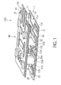
- FIG. 1 to Figure 5 are diagrams for describing the first embodiment of the present invention.
- a module combined body 100 has a power module 1 that controls electric power, and a controlling module 90 that controls the power module 1.
- the module combined body 100 according to this embodiment is an inverter module, for example.
- the controlling module 90 is provided on the upper surface (upper side) of a second insulating substrate 61 (described later) of the power module 1.
- Figure 1 shows such a mode, without being limited to this, the controlling module 90 may be provided on the lower surface (lower side) of a first insulating substrate 11 (described later) of the power module 1.
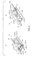
- the power module 1 is provided with a first insulating-substrate-side member 10 that has the first insulating substrate 11, a first conductor layer 12 provided on the upper side of the first insulating substrate 11, and the first electronic elements 31a, 32a provided on the upper side of the first conductor layer 12.
- the power module 1 is provided with a second insulating-substrate-side member 60 that has the second insulating substrate 61, a second conductor layer 62 provided on the upper side of the second insulating substrate 61, and the second electronic elements 31b, 32b provided on the upper side of the second conductor layer 62.
- the second insulating-substrate-side member 60 has not been yet bonded on the first insulating-substrate-side member 10 (see Figure 2 and Figure 3 ), and therefore, is shown while being inverted upside down relative to the configuration of the final power module 1. That is, in the final power module 1, the second conductor layer 62 is provided on the lower side of the second insulating substrate 61, and the second electronic elements 31b, 32b are provided on the lower side of the second conductor layer 62 (see Figure 2 and Figure 3 ).
- the power module 1 has an arrangement structure with a bilateral symmetry (a symmetry with respect to line A 1 -A 1 in Figure 4(a) and line A 2 -A 2 in Figure 4(b) ).
- Ceramic can be raised as an example of the material of the first insulating substrate 11 and the second insulating substrate 61. Copper can be raised as an example of the material of the first conductor layer 12 and the second conductor layer 62.
- a sealing member 80 composed of a resin material or the like is provided between the first insulating substrate 11 and the second insulating substrate 61.
- the sealing member 80 is shown by the "dotted lines”.
- the first electronic elements 31a, 32a and the second electronic elements 31b, 32b are opposingly disposed. Then, the first electronic elements 31a, 32a and the second electronic elements 31b, 32b are connected by an element connecting conductor post 51 that has electric conductivity and linearly extends in the vertical direction. Copper can be raised as an examples of the material of the element connecting conductor post 51. Then, the element connecting conductor post 51 can be formed of a thicker copper foil compared to conductor foils 54a, 54b described later.
- the first electronic elements 31a, 32a have a first switching element 31a and a first rectifying element 32a.
- the second electronic elements 31b, 32b have a second switching element 31b and a second rectifying element 32b.
- the first switching element 31a and the second rectifying element 32b are opposingly disposed, and the second switching element 31b and the first rectifying element 32a are opposingly disposed.
- the element connecting conductor post 51 has a plurality of element connecting conductor post units 51a, 51b.
- the element connecting conductor post unit 51a that is one of the element connecting conductor post units 51a, 51b connects the first switching element 31a and the second rectifying element 32b
- the element connecting conductor post unit 51b that is the other one of the element connecting conductor post units 51a, 51b connects the second switching element 31b and the first rectifying element 32a.
- the switching elements 31a, 31b used in this embodiment that is, the first switching element 31a and the second switching element 31b are respectively a bipolar transistor, for example.
- the rectifying elements 32a, 32b used in this embodiment, that is, the first rectifying element 32a and the second rectifying element 32b are respectively a diode, for example.
- the first conductor layer 12 has a plurality of first conductor layer units 12a to 12d.
- the second conductor layer 62 has a plurality of second conductor layer units 62a to 62c.
- the first switching element 31a is provided on the first conductor layer unit 12b that is one of the first conductor layer units 12a to 12d
- the first rectifying element 32a is provided on the first conductor layer unit 12a that is another one of the first conductor layer units 12a to 12d.
- the second switching element 31b is provide on the second conductor layer unit 62b that is one of the second conductor layer units 62a to 62c
- the second rectifying element 32b is provided on the second conductor layer unit 62a that is another one of the second conductor layer units 62a to 62c.
- the power module 1 further comprises a layer connecting conductor post 52 that connects the first conductor layer units 12a, 12b and the second conductor layer units 62a, 62b.
- the layer connecting conductor post 52 has electric conductivity, and Copper can be raised as an example of the material. Then, for example, the layer connecting conductor post 52 can be formed of a copper foil with substantially the same thickness as the element connecting conductor post 51.
- the layer connecting conductor post 52 has a plurality of layer connecting conductor post units 52a, 52b.
- the layer connecting conductor post unit 52b that is one of the layer connecting conductor post units 52a, 52b is provided on the second conductor layer unit 62a, and connects the second conductor layer unit 62a and the first conductor layer unit 12b.
- the layer connecting conductor post unit 52a that is the other one of the layer connecting conductor post units 52a, 52b is provided on the first conductor layer unit 12a, and connects the first conductor layer unit 12a and the second conductor layer unit 62b.
- the second switching element 31b and the second rectifying element 32b are connected through a conductor foil 53 and the second conductor layer unit 62a.
- the conductor foil 53 is formed of, for example, a copper foil that has electric conductivity, or the like.
- the conductor foil 53 in this embodiment is integral with the element connecting conductor post unit 51b, and laterally extends from a side wall of the element connecting conductor post unit 51b to be connected with the second conductor layer unit 62a.
- a first control terminal 56a is connected with the first switching element 31a through a conductor foil 54a and the first conductor layer unit 12d
- a second control terminal 56b is connected with the second switching element 31b through the second conductor layer unit 62b, a conductor foil 54b and the conductor layer unit 62c.
- external terminals 81 to 83 are connected with the first switching element 31a, the first rectifying element 32a, the second switching element 31b and the second rectifying element 32b, respectively. More concretely, the external terminal 81 is connected with the first rectifying element 32a through the first conductor layer unit 12a. The external terminal 82 is connected with the second rectifying element 32b through the second conductor layer unit 62a. The external terminal 83 is connected with the first switching element 31a through the element connecting conductor post unit 51a, a conductor foil 55 and the first conductor layer unit 12c.
- the conductor foil 55 in this embodiment is integral with the element connecting conductor post unit 51a, and laterally extends from a side wall of the element connecting conductor post unit 51a to be connected with the first conductor layer unit 12c.
- a first radiating member 71 that has thermal conductivity and has a planar shape is provided on the lower side of the first insulating substrate 11.
- a second radiating member 72 that has thermal conductivity and has a planar shape is provided on the upper side of the second insulating substrate 61. Copper can be raised as an example of the material of the first radiating member 71 and the second radiating member 72.
- each of the first radiating member 71 and the second radiating member 72 is a radiator foil, for example, a copper foil.
- the controlling module 90 is provided on the upper surface of the second radiating member 72 composed of a copper foil or the like.
- the first insulating-substrate-side member 10 and the second insulating-substrate-side member 60 are prepared.
- the first insulating-substrate-side member 10 has the first insulating substrate 11, the first conductor layer units 12a to 12d provided on the upper side of the first insulating substrate 11, the first switching element 31a provided on the upper side of the first conductor layer unit 12b that is one of the first conductor layer units 12a to 12d, the first rectifying element 32a provided on the upper side of the first conductor layer unit 12a that is another one of the first conductor layer units 12a to 12d, the element connecting conductor post unit 51a provided on the upper side of the first switching element 31a, the layer connecting conductor post unit 52a provided on the upper side of the first conductor layer unit 12a, and the first radiating member 71 provided on the lower side of the first insulating substrate 11.
- the second insulating-substrate-side member 60 has the second insulating substrate 61, the second conductor layer units 62a to 62c provided on the upper side of the second insulating substrate 61, the second switching element 31b provided on the upper side of the second conductor layer unit 62b that is one of the second conductor layer units 62a to 62c, the second rectifying element 32b provided on the upper side of the second conductor layer unit 62a that is another one of the second conductor layer units 62a to 62c, the element connecting conductor post unit 51b provided on the upper side of the second switching element 31b, the layer connecting conductor post unit 52b provided on the upper side of the second conductor layer unit 62a, and the second radiating member 72 provided on the lower side of the second insulating substrate 61.
- the second insulating-substrate-side member 60 is inverted upside down, and then the first electronic elements 31a, 32a and the second electronic elements 31b, 32b are opposingly disposed (see Figure 2 and Figure 3 ). More concretely, they are disposed such that the second rectifying element 32b is opposed to the first switching element 31a and the second switching element 31b is opposed to the first rectifying element 32a. Then, the first switching element 31a and the second rectifying element 32b are connected by the element connecting conductor post unit 51a provided on the first switching element 31a, and the second switching element 31b is connected to the first rectifying element 32a by the element connecting conductor post unit 51b provided on the second switching element 31b.
- the first conductor layer unit 12b and the second conductor layer unit 62a are connected by the layer connecting conductor post unit 52b provided on the second conductor layer unit 62a, and the first conductor layer unit 12a and the second conductor layer unit 62b are connected by the layer connecting conductor post unit 52a provided on the first conductor layer unit 12a.
- the sealing member 80 is injected and the sealing member 80 is disposed between the first insulating substrate 11 and the second insulating substrate 61 (see Figure 3 ).
- the controlling module 90 is provided on the upper surface (upper side) of the second radiating member 72 of the power module 1, in a manner shown in Figure 1 , and thereby, the module combined body 100 can be produced.
- This embodiment has the first insulating-substrate-side member 10 that has the first insulating substrate 11, the first conductor layer 12 provided on the first insulating substrate 11, and the first electronic elements 31a, 32a provided on the first conductor layer 12, and the second insulating-substrate-side member 60 that has the second insulating substrate 61, the second conductor layer 62 provided on the second insulating substrate 61, and the second electronic elements 31b, 32b provided on the second conductor layer 62 (see Figures 4(a), (b) ).
- the electronic elements 31a, 31b, 32a, 32b are disposed on both of the first insulating-substrate-side member 10 and the second insulating-substrate-side member 60, and the sealing member 80 is provided so as to cover these electronic elements 31a, 31b, 32a, 32b. Therefore, it is possible to dispose the many electronic elements 31a, 31b, 32a, 32b in a small space, without increasing the thickness too much.
- the heat of the first electronic elements 31a, 32a can be primarily radiated from the first insulating substrate 11 side, and the heat of the second electronic elements 31b, 32b can be primarily radiated from the second insulating substrate 61 side. Therefore, it is possible to realize a high heat radiation.
- the heat of the electronic elements 110 that are provided in a planar form can be primarily radiated only from one surface such as the back surface (see Figure 7 ), resulting in an insufficient heat radiation.
- the heat from the first electronic elements 31a, 32a provided on the first insulating substrate 11 side is primarily radiated from the first insulating substrate 11 side
- the heat from the second electronic elements 31b, 32b provided on the second insulating substrate 61 side is primarily radiated from the second insulating substrate 61 side. Therefore, it is possible to realize a high heat radiation.
- the heat from the first electronic elements 31a, 32a can be radiated from the second insulating substrate 61 side through the element connecting conductor post 51, and the heat from the second electronic elements 31b, 32b can be radiated from the first insulating substrate 11 side through the element connecting conductor post 51 and the layer connecting conductor post 52.
- first electronic elements 31a, 32a and the second electronic elements 31b, 32b are opposingly disposed, and the first electronic elements 31a, 32a and the second electronic elements 31b, 32b are connected by the element connecting conductor post 51 that has electric conductivity (see Figure 2 and Figure 3 ).
- the element connecting conductor post 51 that has electric conductivity
- the electronic elements 110 are provided in the planar direction, resulting in a long distance between the electronic elements 110 (see Figure 7 ). Further, conventionally, the electronic elements 110 are connected by the wire 120, resulting in a high electric resistance.
- the first electronic elements 31a, 32a and the second electronic elements 31b, 32b can be opposingly disposed, the first electronic elements 31a, 32a and the second electronic elements 31b, 32b can be positioned at a short distance, and the first electronic elements 31a, 32a and the second electronic elements 31b, 32b can be connected by the element connecting conductor post 51 instead of a wire. Thereby, it is possible to reduce the parasitic inductance and the wiring resistance, compared to the conventional one.
- the first switching element 31a and the second rectifying element 32b are opposed, and the second switching element 31b and the first rectifying element 32a are opposed (see Figure 2 to Figures 4(a) , (b) ). Then, the element connecting conductor post unit 51a connects the first switching element 31a and the second rectifying element 32b, and the element connecting conductor post unit 51b connects the second switching element 31b and the first rectifying element 32a.
- the heat generation from a switching element such as a bipolar transistor is higher compared to the heat generation from a rectifying element such as a diode.
- the first switching element 31a to generate a relatively high heat and the second rectifying element 32b to generate a relatively low heat are close in the vertical direction
- the second switching element 31b to generate a relatively high heat and the first rectifying element 32a to generate a relatively low heat are close in the vertical direction.
- the thickness of the element connecting conductor post units 51a, 51b that connect the first electronic elements 31a, 32a and the second electronic elements 31b, 32b is greater than the thickness of the conductor foil 53 that, in a plane, connects the first switching element 31a and the first rectifying element 32a and connects the second switching element 31b and the second rectifying element 32b.
- the element connecting conductor post units 51a, 51b can have a higher thermal conductivity than the thermal conductivity by the conductor foil 53.
- first switching element 31a to generate a relatively high heat and the second rectifying element 32b to generate a relatively low heat are opposed, and the second switching element 31b to generate a relatively high heat and the first rectifying element 32a to generate a relatively low heat are opposed.
- this embodiment has an arrangement structure with a bilateral symmetry (a symmetry with respect to line A 1 -A 1 in Figure 4(a) and line A 2 -A 2 in Figure 4(b) ), and therefore, it is possible to radiate the heat in a bilaterally-symmetrical and balanced manner.
- the first switching element 31a is provided on the first conductor layer unit 12b, and the first rectifying element 32a is provided on the first conductor layer unit 12a.
- the second switching element 31b is provided on the second conductor layer unit 62b, and the second rectifying element 32b is provided on the second conductor layer unit 62a.
- the layer connecting conductor post unit 52b connects the first conductor layer unit 12b and the second conductor layer unit 62a, and the layer connecting conductor post unit 52a connects the second conductor layer unit 62b and the first conductor layer unit 12a.
- each of the first switching element 31a and the second switching element 31b is an NPN bipolar transistor.
- the terminal on the collector side of the NPN bipolar transistor is connected with the terminal on the cathode side of the diode, and the terminal on the emitter side is connected with the terminal on the anode side of the diode.
- the first switching element 31a and the first rectifying element 32a are connected by the conductor foil 53 instead of a wire
- the second switching element 31b and the second rectifying element 32b are connected by the conductor foil 53 instead of a wire.
- first control terminal 56a is connected with the first switching element 31a
- second control terminal 56b is connected with the second switching element 31b.
- these first control terminal 56a and second control terminal 56b can function as the bases of the switching elements (bipolar transistors) 31a, 31b.
- the external terminal 81 is connected with the first rectifying element 32a
- the external terminal 82 is connected with the second rectifying element 32b
- the external terminal 83 is connected with the first switching element 31a.
- the external terminal 81 can function as the collector
- the external terminal 83 can function as the emitter.
- the external terminal 82 can function as an intermediate terminal.
- the heat radiation can be performed through each of the first control terminal 56a, the second control terminal 56b and the external terminals 81 to 83, and the heat radiation can be performed not only from the normal direction of the planes of the first insulating substrate 11 and the second insulating substrate 61 but also from the extending direction of these planes (hereinafter, referred to as the "in-plane direction").
- the conductor foil 53 is used in this embodiment, and therefore the thermal conductivity in the in-plane direction is also high. Thereby, it is very advantageous that the heat radiation can be performed also from each of the first control terminal 56a, the second control terminal 56b and the external terminals 81 to 83 in this way.
- the heat radiation in the normal direction of the planes of the first insulating substrate 11 and the second insulating substrate 61 is primarily performed in the range of 45 degrees or less from the normal direction.
- the heat radiation in the in-plane direction according to this embodiment is primarily performed in the range other than the range of 45 degrees, resulting in a high heat-radiation efficiency.
- the first radiating member 71 is provided on the lower side of the first insulating substrate 11, and the second radiating member 72 is provided on the upper side of the second insulating substrate 61.
- the above-described first embodiment has a mode of using a "4 in 1" in which four electronic elements are provided, but, without being limited to this, it is possible to use a mode of "'n' in 1" in which "n" electronic elements are provided, such as “2 in 1” in which two electronic elements are provided, or "6 in 1” in which six electronic elements are provided.
- the second embodiment will be described using a mode of "2 in 1" in which two electronic elements are provided, as an example.
- the effects to be achieved have been described in detail in the first embodiment, and therefore, the effects to be achieved in the second embodiment will be appropriately omitted and briefly described.
- the heat of the first electronic elements 31a, 32a can be primarily radiated from the first insulating substrate 11 side, and the heat of the second electronic elements 31b, 32b can be primarily radiated from the second insulating substrate 61 side. Therefore, it is possible to realize a high heat radiation.
- first electronic elements 31a, 32a and the second electronic elements 31b, 32b are positioned at a short distance, and to connect the first electronic elements 31a, 32a and the second electronic elements 31b, 32b by the element connecting conductor post 51 that has a lower electric resistance compared to a wire. Therefore, it is possible to reduce the parasitic inductance and the wiring resistance.
- first switching element 31a to generate a relatively high heat and the second rectifying element 32b to generate a relatively low heat are opposed, and the second switching element 31b to generate a relatively high heat and the first rectifying element 32a to generate a relatively low heat are opposed. Therefore, it is possible to avoid the vertical closing between the switching elements 31a, 31b to generate a high heat. Thereby, it is possible to realize a high heat radiation.
- first switching element 31a and the first rectifying element 32a are connected by the conductor foil 53
- second switching element 31b and the second rectifying element 32b are connected by the conductor foil 53. Therefore, it is possible to reduce the wiring resistance and the parasitic inductance, and consequently to suppress the heat generation. Also, such a reduction in the wiring resistance and the parasitic inductance allows for a decrease in the influence of noise at the time of a switching operation.
- the heat radiation can be performed through each of the first control terminal 56a, the second control terminal 56b and the external terminals 81 to 83. Thereby, the heat radiation can be performed not only from the normal direction of the planes of the first insulating substrate 11 and the second insulating substrate 61 but also from the in-plane direction of the first insulating substrate 11 and the second insulating substrate 61.
- first radiating member 71 and the second radiating member 72 are provided similarly to the first embodiment, it is possible to more increase both the heat radiation in the normal direction of the plane of the first insulating substrate 11 and the heat radiation in the normal direction of the plane of the second insulating substrate 61.
Landscapes
- Engineering & Computer Science (AREA)
- Microelectronics & Electronic Packaging (AREA)
- Power Engineering (AREA)
- Manufacturing & Machinery (AREA)
- Inverter Devices (AREA)
- Cooling Or The Like Of Semiconductors Or Solid State Devices (AREA)
- Dc-Dc Converters (AREA)
- Rectifiers (AREA)
Abstract
Description
- The present invention relates to a module comprising a plurality of electronic elements, a module combined body and a module production method.
- Conventionally, there is known a module in which electronic elements such as transistors and diodes are disposed on a single plane and both faces of these electronic elements are sandwiched by electrodes (see Patent Literature 1, for example). For obtaining a high power in such a module, attempts to increase the sizes of
electronic elements 110 or increase the number ofelectronic elements 110 have been performed (2 in 1, 4 in 1, 6 in 1 and the like) (seeFigure 7 ). - However, on the other hand, the downsizing of the module is desired. When reducing the size of the module while using large-size
electronic elements 110 or using manyelectronic elements 110 as described above, there is a possibility that the heat radiation decreases, resulting in a thermal runaway of the module. - Further, in use of many
electronic elements 110, in the case of connecting theelectronic elements 110 withwires 120 or the like (seeFigure 7 ), the length of thewire 120 increases in some points, leading to an increase in parasitic inductance and wiring resistance. Incidentally,Figure 7 shows a mode of "6 in 1" in which sixelectronic elements 110 are provided. - [Patent Literature 1]
Japanese Patent Laid-Open No. 2005-73342 - In view of the above, the present invention provides a module and a module combined body that make it possible to reduce the size, to maintain the heat radiation, and further to reduce the parasitic inductance and the wiring resistance, even when disposing many electronic elements, and provides a production method of such a module.
- A module according to the present invention comprises:
- a first insulating-substrate-side member that has a first insulating substrate, a first conductor layer provided on an upper side of the first insulating substrate, and a first electronic element provided on an upper side of the first conductor layer;
- a second insulating-substrate-side member that has a second insulating substrate, a second conductor layer provided on a lower side of the second insulating substrate, and a second electronic element provided on a lower side of the second conductor layer; and
- a sealing member that is provided between the first insulating substrate and the second insulating substrate,
- wherein the first electronic element and the second electronic element are opposingly disposed, and
- the first electronic element and the second electronic element are connected by an element connecting conductor post that has electric conductivity.
- In the module according to the present invention,
the first electronic element may have a first switching element and a first rectifying element,
the second electronic element may have a second switching element and a second rectifying element,
the element connecting conductor post may have a plurality of element connecting conductor post units,
one of the element connecting conductor post units may connect the first switching element and the second rectifying element, and
another one of the element connecting conductor post units may connect the second switching element and the first rectifying element. - In the module according to the present invention,
the first conductor layer may have a plurality of first conductor layer units,
the second conductor layer may have a plurality of second conductor layer units,
the first switching element may be provided on one of the first conductor layer units,
the first rectifying element may be provided on another one of the first conductor layer units,
the second switching element may be provided on one of the second conductor layer units, and
the second rectifying element may be provided on another one of the second conductor layer units. - The module according to the present invention, may further comprise a layer connecting conductor post that has electric conductivity and connects the first conductor layer unit and the second conductor layer unit,
wherein the layer connecting conductor post may have a plurality of layer connecting conductor post units,
one of the layer connecting conductor post units may connect the first conductor layer unit on which the first switching element is provided and the second conductor layer unit on which the second rectifying element is provided, and
another one of the layer connecting conductor post units may connect the second conductor layer unit on which the second switching element is provided and the first conductor layer unit on which the first rectifying element is provided. - In the module according to the present invention,
wherein the first switching element and the first rectifying element may be connected by a conductor foil that has electric conductivity, or the second switching element and the second rectifying element may be connected by a conductor foil that has electric conductivity. - The module according to the present invention may further comprise:
- a first control terminal that is connected with the first switching element, and
- a second control terminal that is connected with the second switching element.
- The module according to the present invention may further comprise:
- an external terminal that is connected with the first switching element, the first rectifying element, the second switching element or the second rectifying element.
- In the module according to the present invention,
wherein each of the first switching element and the second switching element may be a bipolar transistor. - In the module according to the present invention,
wherein each of the first rectifying element and the second rectifying element may be a diode. - The module according to the present invention may further comprise:
- a first radiating member that is provided on a lower side of the first insulating substrate, and
- a second radiating member that is provided on an upper side of the second insulating substrate.
- In the module according to the present invention,
each of the first radiating member and the second radiating member may be a radiator foil that has thermal conductivity. - A module combined body according to the present invention comprises:
- a power module that controls electric power; and
- a controlling module that controls the power module,
- wherein the power module is the module according to the present invention, and
- the module combined body is provided on a lower side of the first insulating substrate or an upper side of the second insulating substrate of the power module.
- A module production method according to the present invention comprises:
- preparing a first insulating-substrate-side member that has a first insulating substrate, a first conductor layer provided on an upper side of the first insulating substrate, and a first electronic element provided on an upper side of the first conductor layer;
- preparing a second insulating-substrate-side member that has a second insulating substrate, a second conductor layer provided on an upper side of the second insulating substrate, and a second electronic element provided on an upper side of the second conductor layer;
- inverting the second insulating substrate upside down, opposingly disposing the first electronic element and the second electronic element, and connecting the first electronic element and the second electronic element with an element connecting conductor post that has electric conductivity; and
- injecting a sealing member and disposing the sealing member between the first insulating substrate and the second insulating substrate.
- In the present invention, a first insulating-substrate-side member that has a first insulating substrate, a first conductor layer provided on the first insulating substrate, and a first electronic element provided on the first conductor layer, and a second insulating-substrate-side member that has a second insulating substrate, a second conductor layer provided on the second insulating substrate, and a second electronic element provided on the second conductor layer, are provided. Thereby, it is possible to dispose electronic elements on both of the first insulating-substrate-side member and the second insulating-substrate-side member, and to dispose many electronic elements in a small space.
- Further, the heat of the first electronic element can be primarily radiated from the first insulating substrate side, and the heat of the second electronic element can be primarily radiated from the second insulating substrate side. Therefore, it is possible to realize a high heat radiation.
- Further, the first electronic element and the second electronic element are opposingly disposed, and the first electronic element and the second electronic element are connected by an element connecting conductor post that has electric conductivity. Thereby, it is possible to position the first electronic element and the second electronic element at a short distance, and to connect the first electronic element and the second electronic element by an element connecting conductor post that has a lower electric resistance compared to a wire. Therefore, it is possible to reduce the parasitic inductance and the wiring resistance.
-
- [
Figure 1] Figure 1 is a schematic perspective diagram showing a module according to a first embodiment of the present invention. - [
Figure 2] Figure 2 is a schematic perspective diagram showing a state in which a controlling module is not mounted, in the module according to the first embodiment of the present invention. - [
Figure 3] Figure 3 is a schematic lateral diagram of a mode in which a sealing member is provided in the module shown inFigure 2 , viewed from the lateral direction. - [
Figure 4] Figure 4(a) is a schematic perspective diagram showing a first insulating-substrate-side member andFigure 4(b) is a schematic perspective diagram showing a second insulating-substrate-side member, in the module according to the first embodiment of the present invention. - [
Figure 5] Figure 5 is a diagram showing a circuit that is used in the module according to the first embodiment of the present invention. - [
Figure 6] Figure 6(a) is a schematic perspective diagram showing a first insulating-substrate-side member andFigure 6(b) is a schematic perspective diagram showing a second insulating-substrate-side member, in a module according to a second embodiment of the present invention. - [
Figure 7] Figure 7 is a schematic perspective diagram showing a conventional module. - Hereinafter, a first embodiment of a module, module combined body and module production method according to the present invention will be described with reference to the drawings. Here,
Figure 1 to Figure 5 are diagrams for describing the first embodiment of the present invention. - As shown in
Figure 1 , a module combinedbody 100 according to this embodiment has a power module 1 that controls electric power, and a controllingmodule 90 that controls the power module 1. Here, the module combinedbody 100 according to this embodiment is an inverter module, for example. - In this embodiment, as shown in
Figure 1 , the controllingmodule 90 is provided on the upper surface (upper side) of a second insulating substrate 61 (described later) of the power module 1. AlthoughFigure 1 shows such a mode, without being limited to this, the controllingmodule 90 may be provided on the lower surface (lower side) of a first insulating substrate 11 (described later) of the power module 1. - Hereinafter, this embodiment will be described using a mode of "4 in 1" in which four
electronic elements - As shown in
Figure 4(a) , the power module 1 according to this embodiment is provided with a first insulating-substrate-side member 10 that has the first insulatingsubstrate 11, afirst conductor layer 12 provided on the upper side of the first insulatingsubstrate 11, and the firstelectronic elements first conductor layer 12. Also, as shown inFigure 4(b) , the power module 1 is provided with a second insulating-substrate-side member 60 that has the second insulatingsubstrate 61, asecond conductor layer 62 provided on the upper side of the second insulatingsubstrate 61, and the secondelectronic elements second conductor layer 62. - Here, in
Figure 4(b) , the second insulating-substrate-side member 60 has not been yet bonded on the first insulating-substrate-side member 10 (seeFigure 2 and Figure 3 ), and therefore, is shown while being inverted upside down relative to the configuration of the final power module 1. That is, in the final power module 1, thesecond conductor layer 62 is provided on the lower side of the second insulatingsubstrate 61, and the secondelectronic elements Figure 2 and Figure 3 ). - Incidentally, as shown in
Figures 4(a), (b) , the power module 1 according to this embodiment has an arrangement structure with a bilateral symmetry (a symmetry with respect to line A1-A1 inFigure 4(a) and line A2-A2 inFigure 4(b) ). - Ceramic can be raised as an example of the material of the first insulating
substrate 11 and the second insulatingsubstrate 61. Copper can be raised as an example of the material of thefirst conductor layer 12 and thesecond conductor layer 62. - Furthermore, as shown in
Figure 3 , a sealingmember 80 composed of a resin material or the like is provided between the first insulatingsubstrate 11 and the second insulatingsubstrate 61. InFigure 3 , the sealingmember 80 is shown by the "dotted lines". - The first
electronic elements electronic elements electronic elements electronic elements conductor post 51 that has electric conductivity and linearly extends in the vertical direction. Copper can be raised as an examples of the material of the element connectingconductor post 51. Then, the element connectingconductor post 51 can be formed of a thicker copper foil compared to conductor foils 54a, 54b described later. - As shown in
Figure 4(a) , the firstelectronic elements first switching element 31a and afirst rectifying element 32a. Further, as shown inFigure 4(b) , the secondelectronic elements second switching element 31b and asecond rectifying element 32b. In the power module 1, thefirst switching element 31a and thesecond rectifying element 32b are opposingly disposed, and thesecond switching element 31b and thefirst rectifying element 32a are opposingly disposed. Further, the element connectingconductor post 51 has a plurality of element connectingconductor post units conductor post unit 51a that is one of the element connectingconductor post units first switching element 31a and thesecond rectifying element 32b, and the element connectingconductor post unit 51b that is the other one of the element connectingconductor post units second switching element 31b and thefirst rectifying element 32a. - The
switching elements first switching element 31a and thesecond switching element 31b are respectively a bipolar transistor, for example. The rectifyingelements first rectifying element 32a and thesecond rectifying element 32b are respectively a diode, for example. - As shown in
Figure 4(a) , thefirst conductor layer 12 has a plurality of firstconductor layer units 12a to 12d.
Also, as shown inFigure 4(b) , thesecond conductor layer 62 has a plurality of secondconductor layer units 62a to 62c. Then, as shown inFigure 4(a) , thefirst switching element 31a is provided on the firstconductor layer unit 12b that is one of the firstconductor layer units 12a to 12d, and thefirst rectifying element 32a is provided on the firstconductor layer unit 12a that is another one of the firstconductor layer units 12a to 12d. Further, as shown inFigure 4(b) , thesecond switching element 31b is provide on the secondconductor layer unit 62b that is one of the secondconductor layer units 62a to 62c, and thesecond rectifying element 32b is provided on the secondconductor layer unit 62a that is another one of the secondconductor layer units 62a to 62c. - The power module 1 according to this embodiment further comprises a layer connecting
conductor post 52 that connects the firstconductor layer units conductor layer units conductor post 52 has electric conductivity, and Copper can be raised as an example of the material. Then, for example, the layer connectingconductor post 52 can be formed of a copper foil with substantially the same thickness as the element connectingconductor post 51. - The layer connecting
conductor post 52 has a plurality of layer connectingconductor post units Figure 4(b) , the layer connectingconductor post unit 52b that is one of the layer connectingconductor post units conductor layer unit 62a, and connects the secondconductor layer unit 62a and the firstconductor layer unit 12b. Further, as shown inFigure 4(a) , the layer connectingconductor post unit 52a that is the other one of the layer connectingconductor post units conductor layer unit 12a, and connects the firstconductor layer unit 12a and the secondconductor layer unit 62b. - As shown in
Figure 4(b) , in this embodiment, thesecond switching element 31b and thesecond rectifying element 32b are connected through aconductor foil 53 and the secondconductor layer unit 62a. Theconductor foil 53 is formed of, for example, a copper foil that has electric conductivity, or the like. Incidentally, theconductor foil 53 in this embodiment is integral with the element connectingconductor post unit 51b, and laterally extends from a side wall of the element connectingconductor post unit 51b to be connected with the secondconductor layer unit 62a. - As shown in
Figure 4(a) , afirst control terminal 56a is connected with thefirst switching element 31a through aconductor foil 54a and the firstconductor layer unit 12d, and as shown inFigure 4(b) , asecond control terminal 56b is connected with thesecond switching element 31b through the secondconductor layer unit 62b, aconductor foil 54b and theconductor layer unit 62c. - As shown in
Figures 4(a), (b) ,external terminals 81 to 83 are connected with thefirst switching element 31a, thefirst rectifying element 32a, thesecond switching element 31b and thesecond rectifying element 32b, respectively. More concretely, theexternal terminal 81 is connected with thefirst rectifying element 32a through the firstconductor layer unit 12a. Theexternal terminal 82 is connected with thesecond rectifying element 32b through the secondconductor layer unit 62a. Theexternal terminal 83 is connected with thefirst switching element 31a through the element connectingconductor post unit 51a, aconductor foil 55 and the firstconductor layer unit 12c. Incidentally, theconductor foil 55 in this embodiment is integral with the element connectingconductor post unit 51a, and laterally extends from a side wall of the element connectingconductor post unit 51a to be connected with the firstconductor layer unit 12c. - In this embodiment, as shown in
Figure 2 and Figure 3 , afirst radiating member 71 that has thermal conductivity and has a planar shape is provided on the lower side of the first insulatingsubstrate 11. Also, asecond radiating member 72 that has thermal conductivity and has a planar shape is provided on the upper side of the second insulatingsubstrate 61. Copper can be raised as an example of the material of thefirst radiating member 71 and thesecond radiating member 72. Further, it is possible that each of thefirst radiating member 71 and thesecond radiating member 72 is a radiator foil, for example, a copper foil. In this embodiment, as described above, the controllingmodule 90 is provided on the upper surface of thesecond radiating member 72 composed of a copper foil or the like. - Next, the production method of the power module 1 according to this embodiment will be briefly described.
- First, the first insulating-substrate-
side member 10 and the second insulating-substrate-side member 60 are prepared. - In this embodiment, as shown in
Figure 4(a) , the first insulating-substrate-side member 10 has the first insulatingsubstrate 11, the firstconductor layer units 12a to 12d provided on the upper side of the first insulatingsubstrate 11, thefirst switching element 31a provided on the upper side of the firstconductor layer unit 12b that is one of the firstconductor layer units 12a to 12d, thefirst rectifying element 32a provided on the upper side of the firstconductor layer unit 12a that is another one of the firstconductor layer units 12a to 12d, the element connectingconductor post unit 51a provided on the upper side of thefirst switching element 31a, the layer connectingconductor post unit 52a provided on the upper side of the firstconductor layer unit 12a, and thefirst radiating member 71 provided on the lower side of the first insulatingsubstrate 11. Further, as shown inFigure 4(b) , the second insulating-substrate-side member 60 has the second insulatingsubstrate 61, the secondconductor layer units 62a to 62c provided on the upper side of the second insulatingsubstrate 61, thesecond switching element 31b provided on the upper side of the secondconductor layer unit 62b that is one of the secondconductor layer units 62a to 62c, thesecond rectifying element 32b provided on the upper side of the secondconductor layer unit 62a that is another one of the secondconductor layer units 62a to 62c, the element connectingconductor post unit 51b provided on the upper side of thesecond switching element 31b, the layer connectingconductor post unit 52b provided on the upper side of the secondconductor layer unit 62a, and thesecond radiating member 72 provided on the lower side of the second insulatingsubstrate 61. - Next, the second insulating-substrate-
side member 60 is inverted upside down, and then the firstelectronic elements electronic elements Figure 2 and Figure 3 ). More concretely, they are disposed such that thesecond rectifying element 32b is opposed to thefirst switching element 31a and thesecond switching element 31b is opposed to thefirst rectifying element 32a. Then, thefirst switching element 31a and thesecond rectifying element 32b are connected by the element connectingconductor post unit 51a provided on thefirst switching element 31a, and thesecond switching element 31b is connected to thefirst rectifying element 32a by the element connectingconductor post unit 51b provided on thesecond switching element 31b. At this time, the firstconductor layer unit 12b and the secondconductor layer unit 62a are connected by the layer connectingconductor post unit 52b provided on the secondconductor layer unit 62a, and the firstconductor layer unit 12a and the secondconductor layer unit 62b are connected by the layer connectingconductor post unit 52a provided on the firstconductor layer unit 12a. - After going through the above steps, the sealing
member 80 is injected and the sealingmember 80 is disposed between the first insulatingsubstrate 11 and the second insulating substrate 61 (seeFigure 3 ). - In this way, the power module 1 according to this embodiment is produced.
- Then, the controlling
module 90 is provided on the upper surface (upper side) of thesecond radiating member 72 of the power module 1, in a manner shown inFigure 1 , and thereby, the module combinedbody 100 can be produced. - Next, the operation and effect by this embodiment that has the above-mentioned configuration will be described.
- This embodiment has the first insulating-substrate-
side member 10 that has the first insulatingsubstrate 11, thefirst conductor layer 12 provided on the first insulatingsubstrate 11, and the firstelectronic elements first conductor layer 12, and the second insulating-substrate-side member 60 that has the second insulatingsubstrate 61, thesecond conductor layer 62 provided on the second insulatingsubstrate 61, and the secondelectronic elements Figures 4(a), (b) ). Thereby, it is possible to dispose theelectronic elements side member 10 and the second insulating-substrate-side member 60, and to dispose the manyelectronic elements - That is, conventionally, an increase in the number of the
electronic elements 110 leads to an increase in the size of the module in the planar direction (seeFigure 7 ). Further, since a space for providing a sealing member is required, it is difficult to dramatically decrease the thickness of the module. In contrast, according to this embodiment, theelectronic elements side member 10 and the second insulating-substrate-side member 60, and the sealingmember 80 is provided so as to cover theseelectronic elements electronic elements - Further, according to this embodiment, the heat of the first
electronic elements substrate 11 side, and the heat of the secondelectronic elements substrate 61 side. Therefore, it is possible to realize a high heat radiation. - That is, conventionally, the heat of the
electronic elements 110 that are provided in a planar form can be primarily radiated only from one surface such as the back surface (seeFigure 7 ), resulting in an insufficient heat radiation. In contrast, according to this embodiment, the heat from the firstelectronic elements substrate 11 side is primarily radiated from the first insulatingsubstrate 11 side, and the heat from the secondelectronic elements substrate 61 side is primarily radiated from the second insulatingsubstrate 61 side. Therefore, it is possible to realize a high heat radiation. In addition, according to this embodiment, naturally, the heat from the firstelectronic elements substrate 61 side through the element connectingconductor post 51, and the heat from the secondelectronic elements substrate 11 side through the element connectingconductor post 51 and the layer connectingconductor post 52. - Further, the first
electronic elements electronic elements electronic elements electronic elements conductor post 51 that has electric conductivity (seeFigure 2 and Figure 3 ). Thereby, it is possible to position the firstelectronic elements electronic elements electronic elements electronic elements conductor post 51 that has a lower electric resistance compared to a wire. Therefore, it is possible to reduce the parasitic inductance and the wiring resistance. - That is, conventionally, the
electronic elements 110 are provided in the planar direction, resulting in a long distance between the electronic elements 110 (seeFigure 7 ). Further, conventionally, theelectronic elements 110 are connected by thewire 120, resulting in a high electric resistance. In contrast, according to this embodiment, the firstelectronic elements electronic elements electronic elements electronic elements electronic elements electronic elements conductor post 51 instead of a wire. Thereby, it is possible to reduce the parasitic inductance and the wiring resistance, compared to the conventional one. - Further, in this embodiment, the
first switching element 31a and thesecond rectifying element 32b are opposed, and thesecond switching element 31b and thefirst rectifying element 32a are opposed (seeFigure 2 to Figures 4(a) ,(b) ). Then, the element connectingconductor post unit 51a connects thefirst switching element 31a and thesecond rectifying element 32b, and the element connectingconductor post unit 51b connects thesecond switching element 31b and thefirst rectifying element 32a. - In general, the heat generation from a switching element such as a bipolar transistor is higher compared to the heat generation from a rectifying element such as a diode. In this regard, according to this embodiment, the
first switching element 31a to generate a relatively high heat and thesecond rectifying element 32b to generate a relatively low heat are close in the vertical direction, and thesecond switching element 31b to generate a relatively high heat and thefirst rectifying element 32a to generate a relatively low heat are close in the vertical direction. Thereby, it is possible to avoid the vertical closing between the switchingelements - Here, in this embodiment, the thickness of the element connecting
conductor post units electronic elements electronic elements conductor foil 53 that, in a plane, connects thefirst switching element 31a and thefirst rectifying element 32a and connects thesecond switching element 31b and thesecond rectifying element 32b. Thereby, the element connectingconductor post units conductor foil 53. In such a situation, it is essentially significant that thefirst switching element 31a to generate a relatively high heat and thesecond rectifying element 32b to generate a relatively low heat are opposed, and thesecond switching element 31b to generate a relatively high heat and thefirst rectifying element 32a to generate a relatively low heat are opposed. - Further, as shown in
Figures 4(a), (b) , this embodiment has an arrangement structure with a bilateral symmetry (a symmetry with respect to line A1-A1 inFigure 4(a) and line A2-A2 inFigure 4(b) ), and therefore, it is possible to radiate the heat in a bilaterally-symmetrical and balanced manner. - Further, in this embodiment, the
first switching element 31a is provided on the firstconductor layer unit 12b, and thefirst rectifying element 32a is provided on the firstconductor layer unit 12a. Also, thesecond switching element 31b is provided on the secondconductor layer unit 62b, and thesecond rectifying element 32b is provided on the secondconductor layer unit 62a. Then, the layer connectingconductor post unit 52b connects the firstconductor layer unit 12b and the secondconductor layer unit 62a, and the layer connectingconductor post unit 52a connects the secondconductor layer unit 62b and the firstconductor layer unit 12a. Thereby, as shown inFigure 5 , it is possible to dispose thefirst switching element 31a (inFigure 5 , a bipolar transistor) and thesecond rectifying element 32b (inFigure 5 , a diode) in parallel, and to dispose thesecond switching element 31b (inFigure 5 , a bipolar transistor) and thefirst rectifying element 32a (inFigure 5 , a diode) in parallel. InFigure 5 , the left side is a U-phase, and the right side is a V-phase. - In the mode shown in
Figure 5 , each of thefirst switching element 31a and thesecond switching element 31b is an NPN bipolar transistor. The terminal on the collector side of the NPN bipolar transistor is connected with the terminal on the cathode side of the diode, and the terminal on the emitter side is connected with the terminal on the anode side of the diode. - Further, in this embodiment, the
first switching element 31a and thefirst rectifying element 32a are connected by theconductor foil 53 instead of a wire, and thesecond switching element 31b and thesecond rectifying element 32b are connected by theconductor foil 53 instead of a wire. Thereby, it is possible to reduce the wiring resistance and the parasitic inductance, and consequently to suppress the heat generation. Also, such a reduction in the wiring resistance and the parasitic inductance allows for a decrease in the influence of noise at the time of a switching operation. - Further, in this embodiment, the
first control terminal 56a is connected with thefirst switching element 31a, and thesecond control terminal 56b is connected with thesecond switching element 31b. Thereby, as shown inFigure 5 , thesefirst control terminal 56a andsecond control terminal 56b can function as the bases of the switching elements (bipolar transistors) 31a, 31b. - Further, in this embodiment, the
external terminal 81 is connected with thefirst rectifying element 32a, theexternal terminal 82 is connected with thesecond rectifying element 32b, and theexternal terminal 83 is connected with thefirst switching element 31a. Then, as shown inFigure 5 , theexternal terminal 81 can function as the collector, and theexternal terminal 83 can function as the emitter. Theexternal terminal 82 can function as an intermediate terminal. - Further, in this embodiment, the heat radiation can be performed through each of the
first control terminal 56a, thesecond control terminal 56b and theexternal terminals 81 to 83, and the heat radiation can be performed not only from the normal direction of the planes of the first insulatingsubstrate 11 and the second insulatingsubstrate 61 but also from the extending direction of these planes (hereinafter, referred to as the "in-plane direction"). In this regard, theconductor foil 53 is used in this embodiment, and therefore the thermal conductivity in the in-plane direction is also high. Thereby, it is very advantageous that the heat radiation can be performed also from each of thefirst control terminal 56a, thesecond control terminal 56b and theexternal terminals 81 to 83 in this way. - Here, it is thought that the heat radiation in the normal direction of the planes of the first insulating
substrate 11 and the second insulatingsubstrate 61 is primarily performed in the range of 45 degrees or less from the normal direction. In this regard, the heat radiation in the in-plane direction according to this embodiment is primarily performed in the range other than the range of 45 degrees, resulting in a high heat-radiation efficiency. - Further, in this embodiment, the
first radiating member 71 is provided on the lower side of the first insulatingsubstrate 11, and thesecond radiating member 72 is provided on the upper side of the second insulatingsubstrate 61. Thereby, it is possible to more increase both the heat radiation in the normal direction of the plane of the first insulatingsubstrate 11 and the heat radiation in the normal direction of the plane of the second insulatingsubstrate 61. - Next, a second embodiment of the present invention will be described.
- The above-described first embodiment has a mode of using a "4 in 1" in which four electronic elements are provided, but, without being limited to this, it is possible to use a mode of "'n' in 1" in which "n" electronic elements are provided, such as "2 in 1" in which two electronic elements are provided, or "6 in 1" in which six electronic elements are provided.
- All of such modes can exhibit the same effect as the above-described embodiment.
- The second embodiment will be described using a mode of "2 in 1" in which two electronic elements are provided, as an example. Here, the effects to be achieved have been described in detail in the first embodiment, and therefore, the effects to be achieved in the second embodiment will be appropriately omitted and briefly described.
- First, it is possible to dispose the
electronic elements side member 10 and the second insulating-substrate-side member 60, and to dispose the manyelectronic elements - Further, the heat of the first
electronic elements substrate 11 side, and the heat of the secondelectronic elements substrate 61 side. Therefore, it is possible to realize a high heat radiation. - Further, it is possible to position the first
electronic elements electronic elements electronic elements electronic elements conductor post 51 that has a lower electric resistance compared to a wire. Therefore, it is possible to reduce the parasitic inductance and the wiring resistance. - Further, the
first switching element 31a to generate a relatively high heat and thesecond rectifying element 32b to generate a relatively low heat are opposed, and thesecond switching element 31b to generate a relatively high heat and thefirst rectifying element 32a to generate a relatively low heat are opposed. Therefore, it is possible to avoid the vertical closing between the switchingelements - Further, the
first switching element 31a and thefirst rectifying element 32a are connected by theconductor foil 53, and thesecond switching element 31b and thesecond rectifying element 32b are connected by theconductor foil 53. Therefore, it is possible to reduce the wiring resistance and the parasitic inductance, and consequently to suppress the heat generation. Also, such a reduction in the wiring resistance and the parasitic inductance allows for a decrease in the influence of noise at the time of a switching operation. - Further, the heat radiation can be performed through each of the
first control terminal 56a, thesecond control terminal 56b and theexternal terminals 81 to 83. Thereby, the heat radiation can be performed not only from the normal direction of the planes of the first insulatingsubstrate 11 and the second insulatingsubstrate 61 but also from the in-plane direction of the first insulatingsubstrate 11 and the second insulatingsubstrate 61. - In the case where the
first radiating member 71 and thesecond radiating member 72 are provided similarly to the first embodiment, it is possible to more increase both the heat radiation in the normal direction of the plane of the first insulatingsubstrate 11 and the heat radiation in the normal direction of the plane of the second insulatingsubstrate 61. - Finally, the disclosure of the descriptions and drawings for the above-described embodiments is just one example for explaining the inventions described in the claims, and the inventions described in the claims are not limited by the disclosure of the descriptions or drawings for the above-described embodiments.
-
- 1
- power module
- 10
- first insulating-substrate-side member
- 11
- first insulating substrate
- 12
- first conductor layer
- 12a to 12d
- first conductor layer unit
- 31a
- first switching element (first electronic element)
- 32a
- first rectifying element (first electronic element)
- 31b
- second switching element (second electronic element)
- 32b
- second rectifying element (second electronic element)
- 60
- second insulating-substrate-side member
- 61
- second insulating substrate
- 62
- second conductor layer
- 62a to 62c
- second conductor layer unit
- 51
- element connecting conductor post
- 51a, 51b
- element connecting conductor post unit
- 52
- layer connecting conductor post
- 52a, 52b
- layer connecting conductor post unit
- 53
- conductor foil
- 56a
- first control terminal
- 56b
- second control terminal
- 71
- first radiating member
- 72
- second radiating member
- 80
- sealing member
- 81
- external terminal
- 82
- external terminal
- 83
- external terminal
- 90
- controlling module
- 100
- module combined body
Claims (13)
- A module comprising:a first insulating-substrate-side member that has a first insulating substrate, a first conductor layer provided on an upper side of the first insulating substrate, and a first electronic element provided on an upper side of the first conductor layer;a second insulating-substrate-side member that has a second insulating substrate, a second conductor layer provided on a lower side of the second insulating substrate, and a second electronic element provided on a lower side of the second conductor layer; anda sealing member that is provided between the first insulating substrate and the second insulating substrate,wherein the first electronic element and the second electronic element are opposingly disposed, andthe first electronic element and the second electronic element are connected by an element connecting conductor post that has electric conductivity.
- The module according to claim 1,
wherein the first electronic element has a first switching element and a first rectifying element,
the second electronic element has a second switching element and a second rectifying element,
the element connecting conductor post has a plurality of element connecting conductor post units,
one of the element connecting conductor post units connects the first switching element and the second rectifying element, and
another one of the element connecting conductor post units connects the second switching element and the first rectifying element. - The module according to claim 2,
wherein the first conductor layer has a plurality of first conductor layer units,
the second conductor layer has a plurality of second conductor layer units,
the first switching element is provided on one of the first conductor layer units,
the first rectifying element is provided on another one of the first conductor layer units,
the second switching element is provided on one of the second conductor layer units, and
the second rectifying element is provided on another one of the second conductor layer units. - The module according to claim 3, further comprising:a layer connecting conductor post that has electric conductivity and connects the first conductor layer unit and the second conductor layer unit,wherein the layer connecting conductor post has a plurality of layer connecting conductor post units,one of the layer connecting conductor post units connects the first conductor layer unit on which the first switching element is provided and the second conductor layer unit on which the second rectifying element is provided, andanother one of the layer connecting conductor post units connects the second conductor layer unit on which the second switching element is provided and the first conductor layer unit on which the first rectifying element is provided.
- The module according to any one of claims 2 to 4,
wherein the first switching element and the first rectifying element are connected by a conductor foil that has electric conductivity, or the second switching element and the second rectifying element are connected by a conductor foil that has electric conductivity. - The module according to any one of claims 2 to 5, further comprising:a first control terminal that is connected with the first switching element, anda second control terminal that is connected with the second switching element.
- The module according to any one of claims 2 to 6, further comprising:an external terminal that is connected with the first switching element, the first rectifying element, the second switching element or the second rectifying element.
- The module according to any one of claims 2 to 7,
wherein each of the first switching element and the second switching element is a bipolar transistor. - The module according to any one of claims 2 to 8,
wherein each of the first rectifying element and the second rectifying element is a diode. - The module according to any one of claims 1 to 9, further comprising:a first radiating member that is provided on a lower side of the first insulating substrate, anda second radiating member that is provided on an upper side of the second insulating substrate.
- The module according to claim 10,
wherein each of the first radiating member and the second radiating member is a radiator foil that has thermal conductivity. - A module combined body comprising:a power module that controls electric power; anda controlling module that controls the power module,wherein the power module is the module according to any one of claims 1 to 11, andthe module combined body is provided on a lower side of the first insulating substrate or an upper side of the second insulating substrate of the power module.
- A module production method comprising:preparing a first insulating-substrate-side member that has a first insulating substrate, a first conductor layer provided on an upper side of the first insulating substrate, and a first electronic element provided on an upper side of the first conductor layer;preparing a second insulating-substrate-side member that has a second insulating substrate, a second conductor layer provided on an upper side of the second insulating substrate, and a second electronic element provided on an upper side of the second conductor layer;inverting the second insulating substrate upside down, opposingly disposing the first electronic element and the second electronic element, and connecting the first electronic element and the second electronic element with an element connecting conductor post that has electric conductivity; andinjecting a sealing member and disposing the sealing member between the first insulating substrate and the second insulating substrate.
Applications Claiming Priority (1)
| Application Number | Priority Date | Filing Date | Title |
|---|---|---|---|
| PCT/JP2013/055443 WO2014132397A1 (en) | 2013-02-28 | 2013-02-28 | Module, module assembly, and module manufacturing method |
Publications (3)
| Publication Number | Publication Date |
|---|---|
| EP2963683A1 true EP2963683A1 (en) | 2016-01-06 |
| EP2963683A4 EP2963683A4 (en) | 2016-11-23 |
| EP2963683B1 EP2963683B1 (en) | 2017-08-30 |
Family
ID=51427698
Family Applications (1)
| Application Number | Title | Priority Date | Filing Date |
|---|---|---|---|
| EP13857664.0A Active EP2963683B1 (en) | 2013-02-28 | 2013-02-28 | Module, module assembly, and module manufacturing method |
Country Status (5)
| Country | Link |
|---|---|
| US (1) | US9386698B2 (en) |
| EP (1) | EP2963683B1 (en) |
| JP (1) | JP5657816B1 (en) |
| CN (1) | CN104160503B (en) |
| WO (1) | WO2014132397A1 (en) |
Cited By (1)
| Publication number | Priority date | Publication date | Assignee | Title |
|---|---|---|---|---|
| CN111279471A (en) * | 2017-11-10 | 2020-06-12 | 新电元工业株式会社 | Electronic module |
Families Citing this family (11)
| Publication number | Priority date | Publication date | Assignee | Title |
|---|---|---|---|---|
| CN106463481B (en) * | 2015-04-28 | 2019-11-08 | 新电元工业株式会社 | Semiconductor module and method of manufacturing the same |
| JP6086989B1 (en) | 2015-04-28 | 2017-03-01 | 新電元工業株式会社 | Semiconductor module |
| CN105161477B (en) * | 2015-08-14 | 2019-10-18 | 株洲南车时代电气股份有限公司 | A flat power module |
| CN105070695A (en) * | 2015-08-14 | 2015-11-18 | 株洲南车时代电气股份有限公司 | Bi-side heat radiation electric car power module |
| EP3413349A4 (en) * | 2016-02-03 | 2019-09-11 | Shindengen Electric Manufacturing Co. Ltd. | SEMICONDUCTOR DEVICE, AND MANUFACTURING METHOD THEREOF |
| JP6690280B2 (en) * | 2016-02-12 | 2020-04-28 | 株式会社豊田自動織機 | Semiconductor module |
| JP6473271B1 (en) * | 2017-05-19 | 2019-02-20 | 新電元工業株式会社 | Electronic module |
| WO2019142255A1 (en) * | 2018-01-17 | 2019-07-25 | 新電元工業株式会社 | Electronic module |
| JP7018459B2 (en) * | 2018-01-17 | 2022-02-10 | 新電元工業株式会社 | Electronic module |
| US10517184B2 (en) | 2018-02-09 | 2019-12-24 | Eaton Intelligent Power Limited | Configurable electronics packages |
| CN119050110B (en) * | 2024-10-31 | 2025-03-18 | 北京怀柔实验室 | Power Devices |
Family Cites Families (14)
| Publication number | Priority date | Publication date | Assignee | Title |
|---|---|---|---|---|
| US6350949B1 (en) * | 2000-06-23 | 2002-02-26 | Tyco Electronics Corp | Sealed power distribution module |
| JP3941728B2 (en) * | 2003-04-07 | 2007-07-04 | 富士電機ホールディングス株式会社 | Power semiconductor device |
| JP4075734B2 (en) | 2003-08-21 | 2008-04-16 | 株式会社デンソー | Mounting structure of semiconductor device |
| DE102004019443B3 (en) * | 2004-04-19 | 2005-08-11 | Siemens Ag | Power module has passive semiconductor chip arranged above active semiconductor chip on second film in close contact with surfaces of planar conducting tracks and first film of insulating material with planar conducting tracks |
| JP4635564B2 (en) * | 2004-11-04 | 2011-02-23 | 富士電機システムズ株式会社 | Semiconductor device |
| JP2006186170A (en) * | 2004-12-28 | 2006-07-13 | Nissan Motor Co Ltd | Semiconductor device |
| JP4902560B2 (en) * | 2008-01-28 | 2012-03-21 | 株式会社日立製作所 | Power semiconductor module |
| JP5422466B2 (en) * | 2010-04-01 | 2014-02-19 | 日立オートモティブシステムズ株式会社 | Power converter |
| WO2012157069A1 (en) * | 2011-05-16 | 2012-11-22 | トヨタ自動車株式会社 | Power module |
| US8987777B2 (en) * | 2011-07-11 | 2015-03-24 | International Rectifier Corporation | Stacked half-bridge power module |
| US9041183B2 (en) * | 2011-07-19 | 2015-05-26 | Ut-Battelle, Llc | Power module packaging with double sided planar interconnection and heat exchangers |
| JP2014199829A (en) * | 2011-07-29 | 2014-10-23 | 三洋電機株式会社 | Semiconductor module and inverter mounting the same |
| JP2013038848A (en) * | 2011-08-04 | 2013-02-21 | Honda Motor Co Ltd | Semiconductor device |
| JP2013041939A (en) * | 2011-08-12 | 2013-02-28 | Sanyo Electric Co Ltd | Semiconductor module and inverter mounting the same |
-
2013
- 2013-02-28 JP JP2013558261A patent/JP5657816B1/en active Active
- 2013-02-28 WO PCT/JP2013/055443 patent/WO2014132397A1/en not_active Ceased
- 2013-02-28 CN CN201380002548.3A patent/CN104160503B/en active Active
- 2013-02-28 EP EP13857664.0A patent/EP2963683B1/en active Active
- 2013-02-28 US US14/369,340 patent/US9386698B2/en active Active
Cited By (2)
| Publication number | Priority date | Publication date | Assignee | Title |
|---|---|---|---|---|
| CN111279471A (en) * | 2017-11-10 | 2020-06-12 | 新电元工业株式会社 | Electronic module |
| CN111279471B (en) * | 2017-11-10 | 2023-09-15 | 新电元工业株式会社 | electronic module |
Also Published As
| Publication number | Publication date |
|---|---|
| EP2963683A4 (en) | 2016-11-23 |
| WO2014132397A1 (en) | 2014-09-04 |
| US20150189756A1 (en) | 2015-07-02 |
| JP5657816B1 (en) | 2015-01-21 |
| EP2963683B1 (en) | 2017-08-30 |
| CN104160503B (en) | 2017-03-08 |
| CN104160503A (en) | 2014-11-19 |
| US9386698B2 (en) | 2016-07-05 |
| JPWO2014132397A1 (en) | 2017-02-02 |
Similar Documents
| Publication | Publication Date | Title |
|---|---|---|
| EP2963683B1 (en) | Module, module assembly, and module manufacturing method | |
| US20230171909A1 (en) | Semiconductor device with stacked terminals | |
| JP5067267B2 (en) | Resin-sealed semiconductor device and manufacturing method thereof | |
| US8705257B2 (en) | Switching module including a snubber circuit connected in parallel to a series-connected unit of flowing restriction elements | |
| EP2733743B1 (en) | Power semiconductor module | |
| KR101926854B1 (en) | Semiconductor device | |
| EP2824696B1 (en) | Semiconductor device and method of manufacture thereof | |
| CN105556664B (en) | Semiconductor device | |
| CN101281904B (en) | Semiconductor modules for inverter circuits | |
| US20140334203A1 (en) | Power converter and method for manufacturing power converter | |
| KR101321277B1 (en) | Power module package and method for manufacturing the same | |
| JP6600172B2 (en) | Power module semiconductor device, manufacturing method thereof, and inverter device | |
| EP2717310A1 (en) | Semiconductor device and wiring substrate | |
| US10903149B2 (en) | Semiconductor module, electric vehicle, and power control unit | |
| CN102254895A (en) | Semiconductor device, semiconductor unit, and power semiconductor device | |
| KR20150058015A (en) | Semiconductor device and method for manufacturing same | |
| CN103858228A (en) | Semiconductor device and method of manufacture thereof | |
| US20170133316A1 (en) | Semiconductor device with stacked terminals | |
| US10340816B2 (en) | Semiconductor device and multiphase semiconductor device | |
| US20150270203A1 (en) | Semiconductor device and method of fabricating the same | |
| CN106165089A (en) | Semiconductor module and driving device equipped with semiconductor module | |
| JP2013239501A (en) | Power semiconductor module | |
| US12489095B2 (en) | Semiconductor apparatus | |
| CN209562395U (en) | Intelligent power module, air conditioner | |
| JP2016195179A (en) | Switching element unit |
Legal Events
| Date | Code | Title | Description |
|---|---|---|---|
| PUAI | Public reference made under article 153(3) epc to a published international application that has entered the european phase |
Free format text: ORIGINAL CODE: 0009012 |
|
| 17P | Request for examination filed |
Effective date: 20140604 |
|
| AK | Designated contracting states |
Kind code of ref document: A1 Designated state(s): AL AT BE BG CH CY CZ DE DK EE ES FI FR GB GR HR HU IE IS IT LI LT LU LV MC MK MT NL NO PL PT RO RS SE SI SK SM TR |
|
| AX | Request for extension of the european patent |
Extension state: BA ME |
|
| DAX | Request for extension of the european patent (deleted) | ||
| A4 | Supplementary search report drawn up and despatched |
Effective date: 20161021 |
|
| RIC1 | Information provided on ipc code assigned before grant |
Ipc: H02M 7/00 20060101ALI20161017BHEP Ipc: H05K 1/18 20060101ALI20161017BHEP Ipc: H01L 23/538 20060101ALI20161017BHEP Ipc: H01L 25/18 20060101ALI20161017BHEP Ipc: H01L 25/07 20060101AFI20161017BHEP |
|
| GRAP | Despatch of communication of intention to grant a patent |
Free format text: ORIGINAL CODE: EPIDOSNIGR1 |
|
| INTG | Intention to grant announced |
Effective date: 20170403 |
|
| GRAS | Grant fee paid |
Free format text: ORIGINAL CODE: EPIDOSNIGR3 |
|
| GRAA | (expected) grant |
Free format text: ORIGINAL CODE: 0009210 |
|
| AK | Designated contracting states |
Kind code of ref document: B1 Designated state(s): AL AT BE BG CH CY CZ DE DK EE ES FI FR GB GR HR HU IE IS IT LI LT LU LV MC MK MT NL NO PL PT RO RS SE SI SK SM TR |
|
| REG | Reference to a national code |
Ref country code: GB Ref legal event code: FG4D |
|
| REG | Reference to a national code |
Ref country code: CH Ref legal event code: EP |
|
| REG | Reference to a national code |
Ref country code: AT Ref legal event code: REF Ref document number: 924377 Country of ref document: AT Kind code of ref document: T Effective date: 20170915 |
|
| REG | Reference to a national code |
Ref country code: IE Ref legal event code: FG4D |
|
| REG | Reference to a national code |
Ref country code: DE Ref legal event code: R096 Ref document number: 602013025971 Country of ref document: DE |
|
| REG | Reference to a national code |
Ref country code: NL Ref legal event code: MP Effective date: 20170830 |
|
| REG | Reference to a national code |
Ref country code: LT Ref legal event code: MG4D |
|
| REG | Reference to a national code |
Ref country code: AT Ref legal event code: MK05 Ref document number: 924377 Country of ref document: AT Kind code of ref document: T Effective date: 20170830 |
|
| PG25 | Lapsed in a contracting state [announced via postgrant information from national office to epo] |
Ref country code: AT Free format text: LAPSE BECAUSE OF FAILURE TO SUBMIT A TRANSLATION OF THE DESCRIPTION OR TO PAY THE FEE WITHIN THE PRESCRIBED TIME-LIMIT Effective date: 20170830 Ref country code: FI Free format text: LAPSE BECAUSE OF FAILURE TO SUBMIT A TRANSLATION OF THE DESCRIPTION OR TO PAY THE FEE WITHIN THE PRESCRIBED TIME-LIMIT Effective date: 20170830 Ref country code: HR Free format text: LAPSE BECAUSE OF FAILURE TO SUBMIT A TRANSLATION OF THE DESCRIPTION OR TO PAY THE FEE WITHIN THE PRESCRIBED TIME-LIMIT Effective date: 20170830 Ref country code: SE Free format text: LAPSE BECAUSE OF FAILURE TO SUBMIT A TRANSLATION OF THE DESCRIPTION OR TO PAY THE FEE WITHIN THE PRESCRIBED TIME-LIMIT Effective date: 20170830 Ref country code: LT Free format text: LAPSE BECAUSE OF FAILURE TO SUBMIT A TRANSLATION OF THE DESCRIPTION OR TO PAY THE FEE WITHIN THE PRESCRIBED TIME-LIMIT Effective date: 20170830 Ref country code: NO Free format text: LAPSE BECAUSE OF FAILURE TO SUBMIT A TRANSLATION OF THE DESCRIPTION OR TO PAY THE FEE WITHIN THE PRESCRIBED TIME-LIMIT Effective date: 20171130 |
|
| PG25 | Lapsed in a contracting state [announced via postgrant information from national office to epo] |
Ref country code: RS Free format text: LAPSE BECAUSE OF FAILURE TO SUBMIT A TRANSLATION OF THE DESCRIPTION OR TO PAY THE FEE WITHIN THE PRESCRIBED TIME-LIMIT Effective date: 20170830 Ref country code: IS Free format text: LAPSE BECAUSE OF FAILURE TO SUBMIT A TRANSLATION OF THE DESCRIPTION OR TO PAY THE FEE WITHIN THE PRESCRIBED TIME-LIMIT Effective date: 20171230 Ref country code: LV Free format text: LAPSE BECAUSE OF FAILURE TO SUBMIT A TRANSLATION OF THE DESCRIPTION OR TO PAY THE FEE WITHIN THE PRESCRIBED TIME-LIMIT Effective date: 20170830 Ref country code: BG Free format text: LAPSE BECAUSE OF FAILURE TO SUBMIT A TRANSLATION OF THE DESCRIPTION OR TO PAY THE FEE WITHIN THE PRESCRIBED TIME-LIMIT Effective date: 20171130 Ref country code: GR Free format text: LAPSE BECAUSE OF FAILURE TO SUBMIT A TRANSLATION OF THE DESCRIPTION OR TO PAY THE FEE WITHIN THE PRESCRIBED TIME-LIMIT Effective date: 20171201 Ref country code: ES Free format text: LAPSE BECAUSE OF FAILURE TO SUBMIT A TRANSLATION OF THE DESCRIPTION OR TO PAY THE FEE WITHIN THE PRESCRIBED TIME-LIMIT Effective date: 20170830 |
|
| PG25 | Lapsed in a contracting state [announced via postgrant information from national office to epo] |
Ref country code: NL Free format text: LAPSE BECAUSE OF FAILURE TO SUBMIT A TRANSLATION OF THE DESCRIPTION OR TO PAY THE FEE WITHIN THE PRESCRIBED TIME-LIMIT Effective date: 20170830 |
|
| PG25 | Lapsed in a contracting state [announced via postgrant information from national office to epo] |
Ref country code: DK Free format text: LAPSE BECAUSE OF FAILURE TO SUBMIT A TRANSLATION OF THE DESCRIPTION OR TO PAY THE FEE WITHIN THE PRESCRIBED TIME-LIMIT Effective date: 20170830 Ref country code: PL Free format text: LAPSE BECAUSE OF FAILURE TO SUBMIT A TRANSLATION OF THE DESCRIPTION OR TO PAY THE FEE WITHIN THE PRESCRIBED TIME-LIMIT Effective date: 20170830 Ref country code: CZ Free format text: LAPSE BECAUSE OF FAILURE TO SUBMIT A TRANSLATION OF THE DESCRIPTION OR TO PAY THE FEE WITHIN THE PRESCRIBED TIME-LIMIT Effective date: 20170830 Ref country code: RO Free format text: LAPSE BECAUSE OF FAILURE TO SUBMIT A TRANSLATION OF THE DESCRIPTION OR TO PAY THE FEE WITHIN THE PRESCRIBED TIME-LIMIT Effective date: 20170830 |
|
| PG25 | Lapsed in a contracting state [announced via postgrant information from national office to epo] |
Ref country code: SK Free format text: LAPSE BECAUSE OF FAILURE TO SUBMIT A TRANSLATION OF THE DESCRIPTION OR TO PAY THE FEE WITHIN THE PRESCRIBED TIME-LIMIT Effective date: 20170830 Ref country code: SM Free format text: LAPSE BECAUSE OF FAILURE TO SUBMIT A TRANSLATION OF THE DESCRIPTION OR TO PAY THE FEE WITHIN THE PRESCRIBED TIME-LIMIT Effective date: 20170830 Ref country code: EE Free format text: LAPSE BECAUSE OF FAILURE TO SUBMIT A TRANSLATION OF THE DESCRIPTION OR TO PAY THE FEE WITHIN THE PRESCRIBED TIME-LIMIT Effective date: 20170830 |
|
| REG | Reference to a national code |
Ref country code: DE Ref legal event code: R097 Ref document number: 602013025971 Country of ref document: DE |
|
| PLBE | No opposition filed within time limit |
Free format text: ORIGINAL CODE: 0009261 |
|
| STAA | Information on the status of an ep patent application or granted ep patent |
Free format text: STATUS: NO OPPOSITION FILED WITHIN TIME LIMIT |
|
| 26N | No opposition filed |
Effective date: 20180531 |
|
| PG25 | Lapsed in a contracting state [announced via postgrant information from national office to epo] |
Ref country code: SI Free format text: LAPSE BECAUSE OF FAILURE TO SUBMIT A TRANSLATION OF THE DESCRIPTION OR TO PAY THE FEE WITHIN THE PRESCRIBED TIME-LIMIT Effective date: 20170830 |
|
| REG | Reference to a national code |
Ref country code: CH Ref legal event code: PL |
|
| PG25 | Lapsed in a contracting state [announced via postgrant information from national office to epo] |
Ref country code: MC Free format text: LAPSE BECAUSE OF FAILURE TO SUBMIT A TRANSLATION OF THE DESCRIPTION OR TO PAY THE FEE WITHIN THE PRESCRIBED TIME-LIMIT Effective date: 20170830 |
|
| REG | Reference to a national code |
Ref country code: IE Ref legal event code: MM4A |
|
| REG | Reference to a national code |
Ref country code: BE Ref legal event code: MM Effective date: 20180228 |
|
| PG25 | Lapsed in a contracting state [announced via postgrant information from national office to epo] |
Ref country code: LU Free format text: LAPSE BECAUSE OF NON-PAYMENT OF DUE FEES Effective date: 20180228 Ref country code: LI Free format text: LAPSE BECAUSE OF NON-PAYMENT OF DUE FEES Effective date: 20180228 Ref country code: CH Free format text: LAPSE BECAUSE OF NON-PAYMENT OF DUE FEES Effective date: 20180228 |
|
| REG | Reference to a national code |
Ref country code: FR Ref legal event code: ST Effective date: 20181031 |
|
| PG25 | Lapsed in a contracting state [announced via postgrant information from national office to epo] |
Ref country code: IE Free format text: LAPSE BECAUSE OF NON-PAYMENT OF DUE FEES Effective date: 20180228 |
|
| PG25 | Lapsed in a contracting state [announced via postgrant information from national office to epo] |
Ref country code: BE Free format text: LAPSE BECAUSE OF NON-PAYMENT OF DUE FEES Effective date: 20180228 Ref country code: FR Free format text: LAPSE BECAUSE OF NON-PAYMENT OF DUE FEES Effective date: 20180228 |
|
| PG25 | Lapsed in a contracting state [announced via postgrant information from national office to epo] |
Ref country code: MT Free format text: LAPSE BECAUSE OF NON-PAYMENT OF DUE FEES Effective date: 20180228 |
|
| PG25 | Lapsed in a contracting state [announced via postgrant information from national office to epo] |
Ref country code: TR Free format text: LAPSE BECAUSE OF FAILURE TO SUBMIT A TRANSLATION OF THE DESCRIPTION OR TO PAY THE FEE WITHIN THE PRESCRIBED TIME-LIMIT Effective date: 20170830 |
|
| PG25 | Lapsed in a contracting state [announced via postgrant information from national office to epo] |
Ref country code: PT Free format text: LAPSE BECAUSE OF FAILURE TO SUBMIT A TRANSLATION OF THE DESCRIPTION OR TO PAY THE FEE WITHIN THE PRESCRIBED TIME-LIMIT Effective date: 20170830 |
|
| PG25 | Lapsed in a contracting state [announced via postgrant information from national office to epo] |
Ref country code: MK Free format text: LAPSE BECAUSE OF NON-PAYMENT OF DUE FEES Effective date: 20170830 Ref country code: HU Free format text: LAPSE BECAUSE OF FAILURE TO SUBMIT A TRANSLATION OF THE DESCRIPTION OR TO PAY THE FEE WITHIN THE PRESCRIBED TIME-LIMIT; INVALID AB INITIO Effective date: 20130228 Ref country code: CY Free format text: LAPSE BECAUSE OF FAILURE TO SUBMIT A TRANSLATION OF THE DESCRIPTION OR TO PAY THE FEE WITHIN THE PRESCRIBED TIME-LIMIT Effective date: 20170830 |
|
| PG25 | Lapsed in a contracting state [announced via postgrant information from national office to epo] |
Ref country code: AL Free format text: LAPSE BECAUSE OF FAILURE TO SUBMIT A TRANSLATION OF THE DESCRIPTION OR TO PAY THE FEE WITHIN THE PRESCRIBED TIME-LIMIT Effective date: 20170830 |
|
| REG | Reference to a national code |
Ref country code: DE Ref legal event code: R079 Ref document number: 602013025971 Country of ref document: DE Free format text: PREVIOUS MAIN CLASS: H01L0025070000 Ipc: H10D0080200000 |
|
| PGFP | Annual fee paid to national office [announced via postgrant information from national office to epo] |
Ref country code: GB Payment date: 20260219 Year of fee payment: 14 |
|
| PGFP | Annual fee paid to national office [announced via postgrant information from national office to epo] |
Ref country code: DE Payment date: 20260218 Year of fee payment: 14 |
|
| PGFP | Annual fee paid to national office [announced via postgrant information from national office to epo] |
Ref country code: IT Payment date: 20260224 Year of fee payment: 14 |