EP2960642A1 - Optische kammer für gaserfassungsvorrichtung - Google Patents
Optische kammer für gaserfassungsvorrichtung Download PDFInfo
- Publication number
- EP2960642A1 EP2960642A1 EP15170983.9A EP15170983A EP2960642A1 EP 2960642 A1 EP2960642 A1 EP 2960642A1 EP 15170983 A EP15170983 A EP 15170983A EP 2960642 A1 EP2960642 A1 EP 2960642A1
- Authority
- EP
- European Patent Office
- Prior art keywords
- series
- radiation
- mirrors
- mirror
- optical chamber
- Prior art date
- Legal status (The legal status is an assumption and is not a legal conclusion. Google has not performed a legal analysis and makes no representation as to the accuracy of the status listed.)
- Ceased
Links
- 230000003287 optical effect Effects 0.000 title claims abstract description 55
- 238000001514 detection method Methods 0.000 title claims abstract description 15
- 230000005855 radiation Effects 0.000 claims abstract description 107
- 238000000151 deposition Methods 0.000 claims description 3
- 238000005868 electrolysis reaction Methods 0.000 claims description 3
- PCHJSUWPFVWCPO-UHFFFAOYSA-N gold Chemical compound [Au] PCHJSUWPFVWCPO-UHFFFAOYSA-N 0.000 claims description 3
- 239000010931 gold Substances 0.000 claims description 3
- 229910052737 gold Inorganic materials 0.000 claims description 3
- 238000000465 moulding Methods 0.000 claims description 3
- 238000005240 physical vapour deposition Methods 0.000 description 3
- 230000035945 sensitivity Effects 0.000 description 3
- CURLTUGMZLYLDI-UHFFFAOYSA-N Carbon dioxide Chemical compound O=C=O CURLTUGMZLYLDI-UHFFFAOYSA-N 0.000 description 2
- 229910002092 carbon dioxide Inorganic materials 0.000 description 1
- 239000001569 carbon dioxide Substances 0.000 description 1
- 238000006073 displacement reaction Methods 0.000 description 1
- 235000021183 entrée Nutrition 0.000 description 1
- 239000000463 material Substances 0.000 description 1
- 238000000034 method Methods 0.000 description 1
- 238000001745 non-dispersive infrared spectroscopy Methods 0.000 description 1
- 238000011144 upstream manufacturing Methods 0.000 description 1
Images

Classifications
-
- G—PHYSICS
- G01—MEASURING; TESTING
- G01N—INVESTIGATING OR ANALYSING MATERIALS BY DETERMINING THEIR CHEMICAL OR PHYSICAL PROPERTIES
- G01N21/00—Investigating or analysing materials by the use of optical means, i.e. using sub-millimetre waves, infrared, visible or ultraviolet light
- G01N21/01—Arrangements or apparatus for facilitating the optical investigation
- G01N21/03—Cuvette constructions
- G01N21/0303—Optical path conditioning in cuvettes, e.g. windows; adapted optical elements or systems; path modifying or adjustment
-
- G—PHYSICS
- G01—MEASURING; TESTING
- G01N—INVESTIGATING OR ANALYSING MATERIALS BY DETERMINING THEIR CHEMICAL OR PHYSICAL PROPERTIES
- G01N21/00—Investigating or analysing materials by the use of optical means, i.e. using sub-millimetre waves, infrared, visible or ultraviolet light
- G01N21/01—Arrangements or apparatus for facilitating the optical investigation
- G01N21/03—Cuvette constructions
- G01N21/031—Multipass arrangements
-
- G—PHYSICS
- G01—MEASURING; TESTING
- G01N—INVESTIGATING OR ANALYSING MATERIALS BY DETERMINING THEIR CHEMICAL OR PHYSICAL PROPERTIES
- G01N21/00—Investigating or analysing materials by the use of optical means, i.e. using sub-millimetre waves, infrared, visible or ultraviolet light
- G01N21/17—Systems in which incident light is modified in accordance with the properties of the material investigated
- G01N21/25—Colour; Spectral properties, i.e. comparison of effect of material on the light at two or more different wavelengths or wavelength bands
- G01N21/31—Investigating relative effect of material at wavelengths characteristic of specific elements or molecules, e.g. atomic absorption spectrometry
- G01N21/35—Investigating relative effect of material at wavelengths characteristic of specific elements or molecules, e.g. atomic absorption spectrometry using infrared light
- G01N21/3504—Investigating relative effect of material at wavelengths characteristic of specific elements or molecules, e.g. atomic absorption spectrometry using infrared light for analysing gases, e.g. multi-gas analysis
-
- G—PHYSICS
- G01—MEASURING; TESTING
- G01N—INVESTIGATING OR ANALYSING MATERIALS BY DETERMINING THEIR CHEMICAL OR PHYSICAL PROPERTIES
- G01N21/00—Investigating or analysing materials by the use of optical means, i.e. using sub-millimetre waves, infrared, visible or ultraviolet light
- G01N21/01—Arrangements or apparatus for facilitating the optical investigation
- G01N21/03—Cuvette constructions
- G01N2021/0389—Windows
Definitions
- the present invention relates to an optical chamber for gas detection device and to the gas detection device integrating said optical chamber.
- the invention relates in particular to an NDIR type gas detection device (for "Non-Dispersive Infrared").
- a gas detection device comprising a radiation source arranged to emit light radiation, a radiation detector and reflection means forming an optical chamber into which the emitted light radiation is sent.
- the reflection means comprises a plurality of adjacent reflective surfaces which are arranged such that each radiation emitted by the source is returned directly to the detector by one of the reflecting surfaces.
- the reflective surfaces are each defined by an arc having a radius and a center.
- the object of the invention is to provide an optical chamber for gas detection device allowing the device to have a very satisfactory sensitivity, without increasing its size.
- the device of the invention including said optical chamber will be particularly insensitive to the relative movements of the radiation source and the detector relative to the optical chamber.
- an optical chamber for a gas detection device comprising reflection means for reflecting radiation from a source of radiation and to send it back to a radiation detector.
- the reflection means comprising a first series of adjacent mirrors and a second series of adjacent mirrors.
- the mirrors of the first series and the mirrors of the second series are bifocal.
- the first series of mirrors and the second series of mirrors are arranged relative to each other so that the radiation emitted by the radiation source is reflected alternately by a mirror of the second series and by a mirror of the first series and defines an optical path from the radiation source to the radiation detector.
- the mirrors of the first series and the mirrors of the second series are of ellipsoidal type of truncated revolution.
- the mirrors are arranged so that the optical path followed by the radiation follows a circular path.
- the chamber comprises two parts fixed one on the other, a lower part in which are made the mirrors of the first series and an upper part assembled on the lower part and in which are made the mirrors of the second series.
- the mirrors of the first series and the mirrors of the second series have an ellipsoidal shape and each ellipsoid shape is obtained by molding in the first part and the second part of the optical chamber.
- each mirror has a reflective surface formed by depositing a reflective layer on the ellipsoid shape.
- the reflective layer is deposited by PVD or by electrolysis and comprises for example gold.
- the optical chamber has an input intended to be located vis-à-vis the radiation source and an output intended to be located vis-à-vis the radiation detector.
- the invention also relates to a detection device comprising a radiation source arranged to emit radiation, a radiation detector and an optical chamber in which the gas to be analyzed is located and arranged to transmit radiation from the radiation source to the detector. of radiation, the optical chamber being as defined above.
- the radiation source and the radiation detector are arranged next to each other.
- the radiation source and the radiation detector are fixed on the same electronic card.
- the radiation source comprises at least one light emitting diode.
- the radiation detector comprises at least one photodiode.
- the invention relates to an optical chamber for a gas detection device and the corresponding gas detection device.
- the detection device is intended to determine the concentration of a gas, such as for example carbon dioxide.
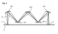
- such a device comprises a radiation source 1 comprising for example at least one light-emitting diode and arranged to emit radiation (R, figure 3 ).
- the device also comprises a radiation detector 2 arranged to detect the radiation emitted by the source 1.
- the detector 2 comprises for example at least one photodiode intended to capture the radiation emitted by the source 1 and transform it into an electrical signal to be processed. .
- the radiation source 1 and the detector 2 are fixed on an electronic card 3 integrated in the device.
- the radiation source and detector are positioned on the map next to each other.
- the device also comprises a closed optical chamber 4, inside which the radiation R is emitted.
- the optical chamber 4, which is the subject of the invention, comprises an input 40 in front of which the radiation source 1 is positioned and an output 41 in front of which is positioned the detector 2 ( figure 2 ).
- the optical chamber 4 comprises reflection means arranged to reflect the radiation R emitted by the source 1 and make it converge towards the detector 2.
- the reflection means comprise a first series of adjacent mirrors Mi and a second series of adjacent mirrors M'i.
- the first series of mirrors Mi and the second series of mirrors M'i are arranged so that the radiation R emitted by the source 1 is reflected and focused alternately by a mirror of the second series and then by a mirror of the first series of following a zigzag-shaped optical path from the radiation source 1 to the detector 2.
- the optical chamber employs bifocal mirrors. Each mirror thus comprises, if one follows the optical path, a first focus located upstream of the mirror and a second focus located downstream of the mirror.
- the process described above continues between mirrors of the first series and mirrors of the second series until the radiation reaches the detector 2.
- the mirrors are thus arranged to advance the radiation inside the optical chamber. from the radiation source 1 to the detector 2.
- the use of bifocals makes it possible to focus the radiation from the source to the detector and thus obtain a device of great sensitivity.
- the bifocals used in the first series and in the second series are ellipsoid truncated revolution type.
- the ellipsoid shape of truncated revolution gives the mirror the property of having two foci, which makes it possible, thanks to the arrangement of the invention, to focus a maximum of the radiation on the detector 2 and to limit the bounces inside the the optical chamber 4.
- the first mirror M'1 of the second series is oriented so as to focus the radiation towards the first mirror M1 of the first series while being in line with the radiation source 1 and having the source of radiation 1 located at his first home.
- the last mirror M'n is located directly above the detector 2 and is oriented so as to focus the radiation coming from the mirror Mn-1 of the first series towards the detector 2, the detector being located at its second focus.
- Each mirror is for example made by depositing a reflective layer on a piece of plastic material.
- the reflective layer is for example a layer of gold deposited by PVD ("Physical Vapor Deposition") or by electrolysis.
- the optical chamber 4 is formed of two distinct parts 42, 43 attached to one another, an upper portion 43 being fixed on a lower portion 42 so as to obtain a closed optical chamber.
- a screw 44 is for example provided for fixing the two parts together.
- the mirrors Mi of the first series are formed in the lower part 42 and the mirrors M'i of the second series are formed in the upper part 43.
- the lower part 42 has a first opening forming said input 40 of the radiation and a second opening forming said output 41 of the radiation R.
- the ellipsoid shape of the mirrors is obtained by molding in the first portion 42 and in the second portion 43 of the optical chamber.
- the radiation produced inside the chamber passes through each time the junction plane of the lower part and the upper part of the chamber.
- the mirrors of the first series and the mirrors of the second series are thus placed in two distinct planes parallel to the joining plane defined above.
- the mirrors Mi, M'i of the first series and of the second series are arranged so that the radiation follows a circular optical path to inside the room. This arrangement makes it possible in particular to obtain an optical path that is as long as possible while limiting the size of the device.
- the optical chamber 4 is fixed directly, by its first part 42, on the electronic card 3 so that the radiation source 1 and the detector 2 is in vis-à-vis respectively of the input 40 of the optical chamber and the output 41 of the optical chamber.
- the device may comprise integrated processing means (not shown) making it possible to analyze the electrical signal obtained at the output of the detector 2 with respect to the signal emitted by the source 1 in order to deduce therefrom the concentration of the gas present in the optical chamber. 3. These processing means may also be independent of the device and separated therefrom.
Landscapes
- Physics & Mathematics (AREA)
- Health & Medical Sciences (AREA)
- Life Sciences & Earth Sciences (AREA)
- Chemical & Material Sciences (AREA)
- Analytical Chemistry (AREA)
- Biochemistry (AREA)
- General Health & Medical Sciences (AREA)
- General Physics & Mathematics (AREA)
- Immunology (AREA)
- Pathology (AREA)
- Spectroscopy & Molecular Physics (AREA)
- Investigating Or Analysing Materials By Optical Means (AREA)
Applications Claiming Priority (2)
| Application Number | Priority Date | Filing Date | Title |
|---|---|---|---|
| FR1455984 | 2014-06-26 | ||
| FR1456055A FR3022999B1 (fr) | 2014-06-27 | 2014-06-27 | Chambre optique pour dispositif de detection de gaz |
Publications (1)
| Publication Number | Publication Date |
|---|---|
| EP2960642A1 true EP2960642A1 (de) | 2015-12-30 |
Family
ID=53269416
Family Applications (1)
| Application Number | Title | Priority Date | Filing Date |
|---|---|---|---|
| EP15170983.9A Ceased EP2960642A1 (de) | 2014-06-26 | 2015-06-08 | Optische kammer für gaserfassungsvorrichtung |
Country Status (3)
| Country | Link |
|---|---|
| US (1) | US9645073B2 (de) |
| EP (1) | EP2960642A1 (de) |
| CN (1) | CN105223151B (de) |
Families Citing this family (6)
| Publication number | Priority date | Publication date | Assignee | Title |
|---|---|---|---|---|
| FR3069334B1 (fr) * | 2017-07-21 | 2019-10-18 | Commissariat A L'energie Atomique Et Aux Energies Alternatives | Cavite optique a forte dynamique |
| GB201812766D0 (en) * | 2018-08-06 | 2018-09-19 | Res & Innovation Uk | Optical multi-pass cells |
| DE102018215587A1 (de) * | 2018-09-13 | 2020-03-19 | Osram Opto Semiconductors Gmbh | Strahlleitende kavitätsstrukur, gassensor und verfahren zum herstellen der derselben |
| FR3095517B1 (fr) * | 2019-04-25 | 2021-05-14 | Elichens | Capteur de gaz compact |
| KR102267044B1 (ko) * | 2019-12-11 | 2021-06-18 | 주식회사 태성환경연구소 | 비분산적외선 방식의 이산화탄소 가스센서 |
| SE543968C2 (en) * | 2020-02-27 | 2021-10-12 | Senseair Ab | Gas sensor with long absorption path length |
Citations (7)
| Publication number | Priority date | Publication date | Assignee | Title |
|---|---|---|---|---|
| DE4214840A1 (de) * | 1992-05-05 | 1993-11-11 | Draegerwerk Ag | Vorrichtung zur gleichzeitigen Analyse verschiedener Bestandteile eines Fluids |
| WO1998009152A1 (en) * | 1996-08-28 | 1998-03-05 | Martin Hans Goeran Evald | Gas sensor |
| EP1059708A1 (de) * | 1998-11-10 | 2000-12-13 | Tokyo Denshi Kabushiki Kaisha | Grät für photoreaktion |
| WO2002063283A1 (en) * | 2001-02-08 | 2002-08-15 | Dynament Limited | Gas sensor |
| US20060227327A1 (en) * | 2005-04-08 | 2006-10-12 | Mcneal Mark P | Absorption spectroscopy apparatus and method |
| EP1987346B1 (de) | 2006-02-06 | 2010-08-11 | Gas Sensing Solutions Limited | Kuppelgassensor |
| EP2526404A1 (de) | 2010-01-18 | 2012-11-28 | Gas Sensing Solutions Ltd | Gassensor mit strahlungsführung |
Family Cites Families (9)
| Publication number | Priority date | Publication date | Assignee | Title |
|---|---|---|---|---|
| DE3830906A1 (de) * | 1988-09-10 | 1990-03-15 | Draegerwerk Ag | Spiegelanordnung fuer einen strahlengang in einer vielfach-reflexionsmesszelle |
| US5065025A (en) * | 1990-03-02 | 1991-11-12 | Axiom Analytical, Inc. | Gas sample analysis provided by light pipe radiation structure |
| US5515859A (en) * | 1993-08-24 | 1996-05-14 | Colorado Health Care Research Corp. | Myocardial infarction and ischemia detection method and apparatus |
| JP3228080B2 (ja) * | 1995-08-07 | 2001-11-12 | 富士電機株式会社 | 多重反射形試料セル |
| US7034304B2 (en) * | 2003-07-25 | 2006-04-25 | Honeywell International, Inc. | Chamber for gas detector |
| CN1985160A (zh) * | 2004-07-22 | 2007-06-20 | 光屋环球解决方案有限公司 | 针对颗粒传感器系统的改进设计 |
| JP4895294B2 (ja) * | 2007-01-30 | 2012-03-14 | 東京エレクトロン株式会社 | パーティクルモニタシステム及び基板処理装置 |
| CN201681044U (zh) * | 2010-03-25 | 2010-12-22 | 友丽系统制造股份有限公司 | 光电式气体感测模块及其装置 |
| US8785857B2 (en) * | 2011-09-23 | 2014-07-22 | Msa Technology, Llc | Infrared sensor with multiple sources for gas measurement |
-
2015
- 2015-06-08 EP EP15170983.9A patent/EP2960642A1/de not_active Ceased
- 2015-06-15 US US14/739,103 patent/US9645073B2/en active Active
- 2015-06-26 CN CN201510581542.7A patent/CN105223151B/zh active Active
Patent Citations (7)
| Publication number | Priority date | Publication date | Assignee | Title |
|---|---|---|---|---|
| DE4214840A1 (de) * | 1992-05-05 | 1993-11-11 | Draegerwerk Ag | Vorrichtung zur gleichzeitigen Analyse verschiedener Bestandteile eines Fluids |
| WO1998009152A1 (en) * | 1996-08-28 | 1998-03-05 | Martin Hans Goeran Evald | Gas sensor |
| EP1059708A1 (de) * | 1998-11-10 | 2000-12-13 | Tokyo Denshi Kabushiki Kaisha | Grät für photoreaktion |
| WO2002063283A1 (en) * | 2001-02-08 | 2002-08-15 | Dynament Limited | Gas sensor |
| US20060227327A1 (en) * | 2005-04-08 | 2006-10-12 | Mcneal Mark P | Absorption spectroscopy apparatus and method |
| EP1987346B1 (de) | 2006-02-06 | 2010-08-11 | Gas Sensing Solutions Limited | Kuppelgassensor |
| EP2526404A1 (de) | 2010-01-18 | 2012-11-28 | Gas Sensing Solutions Ltd | Gassensor mit strahlungsführung |
Also Published As
| Publication number | Publication date |
|---|---|
| US20150377767A1 (en) | 2015-12-31 |
| CN105223151B (zh) | 2019-07-12 |
| CN105223151A (zh) | 2016-01-06 |
| US9645073B2 (en) | 2017-05-09 |
Similar Documents
| Publication | Publication Date | Title |
|---|---|---|
| EP2960642A1 (de) | Optische kammer für gaserfassungsvorrichtung | |
| FR3046851B1 (fr) | Guide optique ameliore et systeme optique | |
| EP2277074B1 (de) | Informative brille | |
| EP1712940B1 (de) | Gleichmässige Beleuchtungsvorrichtung bestehend aus einer Matrix von Laserdioden | |
| FR2995977A1 (fr) | Guide de lumiere pour un dispositif d'eclairage et/ou de signalisation de vehicule automobile | |
| WO2010072362A1 (fr) | Guide d'onde perfectionné et spectromètre associé embarqué dans un véhicule automobile | |
| FR3022999A1 (fr) | Chambre optique pour dispositif de detection de gaz | |
| FR2966223A1 (fr) | Dispositif d'eclairage ou de signalisation | |
| FR2712985A1 (fr) | Tête de mesure colorimétrique, et procédé pour déterminer la couleur interne d'un matériau non opaque. | |
| EP2703852A1 (de) | Lichtleitungslage mit Eingangskoppelung und Diopter mit Fresnel-Oberfläche | |
| FR3063811A1 (fr) | Capteur optique de gaz | |
| FR2828281A1 (fr) | Dispositif pour l'analyse d'un echantillon notamment par cytometrie de flux | |
| Avila et al. | High efficiency inexpensive 2-slices image slicers | |
| WO2011067341A1 (fr) | Reflecteur optique a lames semi-reflechissantes pour dispositif de detection de position de casque et casque comportant un tel dispositif | |
| EP1657833B1 (de) | Photoelektrischer Detektor | |
| FR2774475A1 (fr) | Dispositif de telemetrie optique | |
| EP2952951B1 (de) | Erfassungssystem | |
| EP3583402A1 (de) | Optischer partikeldetektor | |
| JP7264134B2 (ja) | 分光分析装置、光学系、及び方法 | |
| KR101109148B1 (ko) | 표면 플라즈몬 공진 센서 및 표면 플라즈몬 공진을 이용한 센싱 방법 | |
| EP3785061B1 (de) | Lichtleiter für gestendetektionsschnittstellenmodul | |
| CN102608075A (zh) | 一种毛细管表面等离子共振传感器 | |
| EP3563288B1 (de) | Strichcode-leser | |
| JP6599675B2 (ja) | 光学式センサ | |
| EP3850339A1 (de) | Kompakter gassensor |
Legal Events
| Date | Code | Title | Description |
|---|---|---|---|
| PUAI | Public reference made under article 153(3) epc to a published international application that has entered the european phase |
Free format text: ORIGINAL CODE: 0009012 |
|
| AK | Designated contracting states |
Kind code of ref document: A1 Designated state(s): AL AT BE BG CH CY CZ DE DK EE ES FI FR GB GR HR HU IE IS IT LI LT LU LV MC MK MT NL NO PL PT RO RS SE SI SK SM TR |
|
| AX | Request for extension of the european patent |
Extension state: BA ME |
|
| 17P | Request for examination filed |
Effective date: 20160112 |
|
| RBV | Designated contracting states (corrected) |
Designated state(s): AL AT BE BG CH CY CZ DE DK EE ES FI FR GB GR HR HU IE IS IT LI LT LU LV MC MK MT NL NO PL PT RO RS SE SI SK SM TR |
|
| STAA | Information on the status of an ep patent application or granted ep patent |
Free format text: STATUS: THE APPLICATION HAS BEEN REFUSED |
|
| 18R | Application refused |
Effective date: 20200110 |