EP2959331B1 - Élément dispersant le rayonnement électromagnétique - Google Patents
Élément dispersant le rayonnement électromagnétique Download PDFInfo
- Publication number
- EP2959331B1 EP2959331B1 EP14705802.8A EP14705802A EP2959331B1 EP 2959331 B1 EP2959331 B1 EP 2959331B1 EP 14705802 A EP14705802 A EP 14705802A EP 2959331 B1 EP2959331 B1 EP 2959331B1
- Authority
- EP
- European Patent Office
- Prior art keywords
- elevations
- height
- electromagnetic radiation
- wavelength
- surface profile
- Prior art date
- Legal status (The legal status is an assumption and is not a legal conclusion. Google has not performed a legal analysis and makes no representation as to the accuracy of the status listed.)
- Active
Links
Images


Classifications
-
- G—PHYSICS
- G02—OPTICS
- G02B—OPTICAL ELEMENTS, SYSTEMS OR APPARATUS
- G02B5/00—Optical elements other than lenses
- G02B5/02—Diffusing elements; Afocal elements
- G02B5/0205—Diffusing elements; Afocal elements characterised by the diffusing properties
- G02B5/021—Diffusing elements; Afocal elements characterised by the diffusing properties the diffusion taking place at the element's surface, e.g. by means of surface roughening or microprismatic structures
- G02B5/0221—Diffusing elements; Afocal elements characterised by the diffusing properties the diffusion taking place at the element's surface, e.g. by means of surface roughening or microprismatic structures the surface having an irregular structure
-
- G—PHYSICS
- G01—MEASURING; TESTING
- G01B—MEASURING LENGTH, THICKNESS OR SIMILAR LINEAR DIMENSIONS; MEASURING ANGLES; MEASURING AREAS; MEASURING IRREGULARITIES OF SURFACES OR CONTOURS
- G01B11/00—Measuring arrangements characterised by the use of optical techniques
- G01B11/24—Measuring arrangements characterised by the use of optical techniques for measuring contours or curvatures
-
- G—PHYSICS
- G02—OPTICS
- G02B—OPTICAL ELEMENTS, SYSTEMS OR APPARATUS
- G02B27/00—Optical systems or apparatus not provided for by any of the groups G02B1/00 - G02B26/00, G02B30/00
- G02B27/0012—Optical design, e.g. procedures, algorithms, optimisation routines
-
- G—PHYSICS
- G02—OPTICS
- G02B—OPTICAL ELEMENTS, SYSTEMS OR APPARATUS
- G02B5/00—Optical elements other than lenses
- G02B5/02—Diffusing elements; Afocal elements
- G02B5/0268—Diffusing elements; Afocal elements characterized by the fabrication or manufacturing method
-
- G—PHYSICS
- G02—OPTICS
- G02B—OPTICAL ELEMENTS, SYSTEMS OR APPARATUS
- G02B5/00—Optical elements other than lenses
- G02B5/02—Diffusing elements; Afocal elements
- G02B5/0273—Diffusing elements; Afocal elements characterized by the use
- G02B5/0284—Diffusing elements; Afocal elements characterized by the use used in reflection
-
- G—PHYSICS
- G02—OPTICS
- G02B—OPTICAL ELEMENTS, SYSTEMS OR APPARATUS
- G02B5/00—Optical elements other than lenses
- G02B5/18—Diffraction gratings
Definitions
- the invention relates to an optical element that diffusely scatters electromagnetic radiation and to a method for its production.
- optical elements can be used in almost all projection applications, such as front and rear projection, display applications, (cinema) screens and the like.
- the structures described can be used to homogenize and align light sources. This also opens up areas of application in general lighting, in which case a distribution of the luminance can be controlled by such a diffuser.
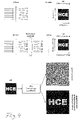
- these optical elements can be used for applications in the field of static projection and for structured lighting, for example to generate patterns, symbols, lettering or logos.
- Diffusers and lenses are used in many microdisplay and projection applications deployed.
- the image is created on a diffusing screen, which the viewer can view directly or in an intermediate image plane of an optical system.
- the task of the diffuser is to scatter the light from the image plane as evenly as possible into the spatial area in which, for example, the viewer can be located. In most applications it is possible to strongly delimit this area of space, the so-called eyebox. Ideally, all of the light should be scattered from the diffuser into the eyebox. With a homogeneous distribution of the luminance inside the eyebox, with minimum intensity outside at the same time, the efficiency of the projector is optimal and there are no brightness fluctuations in the event of a change of location or the viewer's viewing angle lateral to the projection screen.
- diffusers can be used to realize a specific radiation characteristic, as is important in lighting applications, for example. It can be used to generate specific angular distributions of the light source. For example, it is possible to generate any desired intensity distribution in the far field from a collimated light source. With very strong collimated sources. such as lasers, this can be used to generate images and can be used in the area of static image generation (projection of lettering, logos, graphics). It is also possible to define a scattering element in a spatially resolved manner, i.e. to use laterally different scattering functions. This can be used, for example, to tilt the scatter distribution according to a lens function, to collimate a light source or to compensate for parallax errors in the case of extensive scatter screens.
- diffractive optical elements With diffractive optical elements it is possible to precisely define the characteristics of a scattering distribution of the electromagnetic radiation.
- the surface profile of a diffractive optical element is calculated using an iterative Fourier Transform Algorithm (IFTA).
- IFTA iterative Fourier Transform Algorithm
- the scatter distribution can be specified almost arbitrarily with regard to intensity and angular distribution.
- diffractive diffusers have so far been of little importance, since they have a strong wavelength dependence and only a limited proportion of the light passes through this diffuser in scattered form.
- a non-negligible proportion passes through the element unhindered and results in a disturbing 0th diffraction order, which is reflected in the direct visibility of the respective light source for the viewer.
- the production of such elements especially when high radiation angles are required, can hardly be realized with today's technologies or only with considerable effort.
- Lens arrays represent a widespread possibility for the realization of diffusers and diffusers, especially with incoherent illumination. Due to the periodic or regular structures that occur in a lens array, undesired diffraction patterns occur in the case of strongly collimated or spectrally narrow-band illumination. For technological reasons, the fill factor of lens arrays can usually not be arbitrarily high. So-called dead zones between the lenses then cause the light to pass through the diffuser without being scattered (similar to the 0th order of diffraction with diffractive elements). In addition, scattering distributions that can be realized with microlens arrays are severely limited in terms of their shape and intensity distribution. They are mostly limited to the illumination of geometrically simple shapes such as rectangles or circles.
- volume holograms or so-called effective ones Medium CGHs, the production of which is very complex and which, like surface-structured optics, cannot be replicated or copied by moulding, spraying or embossing processes and which also only work as desired for a narrow wavelength range.
- WO 2011/149715 A1 is a layer with which light can be directed back and a display system with such optical layers is known.
- US 2012/0268964 A1 discloses a diffuser sheet with controlled light collimation.
- U.S. 2006/0279679 A1 discloses a layer that condenses light and a method of manufacture.
- Algorithms are also known with which a predetermined surface structuring can be achieved, such as in Lars-Christian Wittig: "Continuous surface profiles for optical beam shaping", dissertation, Council of the Faculty of Physics and Astronomy, Friedrich Schiller University, Jena, July 6, 2005, pages 1-109, XP002751360 .
- this object is achieved with an optical element in which the features of claim 1 are implemented. It can be produced by a method according to claim 5.
- Advantageous refinements and developments of the invention can be achieved with the features specified in the subordinate claims.
- An optical element according to the invention that diffusely scatters electromagnetic radiation can be formed from a material that is transparent to the electromagnetic radiation and can be designed for electromagnetic radiation from the wavelength spectrum of light.
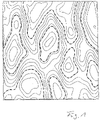
- a surface profile that does not form a repeating regular surface structure is present on a surface.
- elevations are formed as structural elements of the surface structure, which have a height with which a phase shift ⁇ that is greater than two and a half times the largest wavelength used is achieved.
- the elevations have a lateral extent in each plane in all axial directions that is greater than five times the largest wavelength used.
- the individual elevations are continuous in the three spatial axis directions and no edges, shoulders, cracks or profiling are formed on the elevations and there are no elevations in the form of a second-order surface.
- the height of ridges is to be understood as the distance between the position at which a ridge is farthest from the deepest point of a depression formed adjacent to the ridge.
- the lateral extension should be as large in all axial directions, ie around 360° around the centroid of the largest cross-sectional area of an elevation, as five times the largest wavelength used with which the element is irradiated.
- a continuous formation in the three spatial axis directions is to be understood as meaning a non-symmetrical formation or geometric shape in which the surface changes continuously from one position to each adjacent position and therefore there are no edges, steps, cracks or profiling.
- no constant angles of inclination or a surface contour following a radius should occur in the three spatial axis directions (x, y and z direction).
- the angle of inclination or curvature along the surface should not be the same or change evenly, but should not change suddenly. This differs from the prior art microlenses, where the slope changes abruptly at boundaries between adjacent microlenses.
- the geometric shape and dimensioning of each individual elevation should be calculated using a deterministic computing algorithm, and as a result no random formation of elevations should occur.
- the calculation should be carried out using an iterative Fourier transformation algorithm.
- An element according to the invention has an advantageous effect when collimated electromagnetic radiation is used.
- a collimated laser beam can be directed onto the surface on which the surface profile is formed. Due to the scattering effect that can be achieved, a significantly larger area can be illuminated or appear luminous than would be expected from the area of the beam cross section of the laser beam. Due to the possible avoidance or suppression of the zeroth order of diffraction, the punctiform laser beam source is not visible or is only very indistinctly visible or is imaged as such.
- No elevation of the surface structure should have the same geometric shape and/or height and/or volume have, which corresponds to a further elevation of the surface structure of the element.
- Each individual elevation can thus be geometrically shaped and dimensioned individually.
- the respective angle of incidence of the electromagnetic radiation, the desired deflection angle ⁇ of the radiation, its position, the size or distance of an eyebox, the wavelength spectrum used or a selected wavelength of electromagnetic radiation, taking into account the optical refractive index of the material from the an element according to the invention is taken into account when designing the surface structure to be formed. With the individually designed and dimensioned Complete asymmetry can be achieved with elevations.
- An element according to the invention is designed for a wavelength spectrum in the range between 200 nm and 1200 nm.
- An element according to the invention can have a predeterminable scattering distribution in a wavelength range that is greater than ⁇ 3% of a central wavelength of the wavelength spectrum used. This is advantageous since, in the case of diffractive elements, a strong zeroth or higher diffraction order forms even with a very small deviation from the wavelength for which they are manufactured.
- the scatter distribution of the electromagnetic radiation used can change depending on the position of impingement of the electromagnetic radiation (light) from the radiation source on the element, for example by tilting the center of gravity of the scatter distribution.
- the production takes place by methods known per se, in which a locally targeted removal of material takes place, but also by moulding, (injection) casting, (injection) embossing of a tool.
- the invention ties in with the diffractive diffusers already described.
- the existence of the zeroth diffraction order and the wavelength dependence of these elements is due to the existence of discontinuities in the surface profile, which occur as a result of 2 ⁇ jumps in the phase function of the optical function.
- the height of these jumps can only be set precisely for one wavelength and with a material of an optical element with a constant optical refractive index.
- the phase ⁇ can be approximately determined as the quotient of the product of the thickness or the height of a structural element (elevation) h and the difference in the optical refractive index between the material of the element and the environment ⁇ n, divided by the respective wavelength ⁇ . Consequently, the thickness or height h has an influence on the achievable phase jump ⁇ . Jumps in the phase function have the same effect as in an optical diffraction grating.
- the radiated angular distribution scales according to the grating equation with the wavelength ⁇ and the periods p that occur and the diffraction order m .
- sin a m ⁇ ⁇ p
- the edge of the recess results in very high spatial frequencies in the surface profile, which can hardly be realized when manufacturing diffractive elements. This results in a rounding of the edges and a shape deviation of the phase function, which would adversely affect the scatter distribution in terms of homogeneity and efficiency. These and other manufacturing defects in the surface profile cause this.
- phase dislocations also lead to undesired scattered light and transmission in direction due to production the zeroth order of diffraction, which is intensified even further in the case of broadband illumination with electromagnetic radiation from a larger wavelength range.
- phase displacement due to the existence of phase displacement, it is not possible to convert the optical function calculated by a conventional IFTA into a smooth surface profile that does not contain any 2 ⁇ phase jumps.
- the invention uses a modification of an IFTA in which no phase dislocations occur.
- the phase function is not optimized in the developed design algorithm, but rather the surface profile with the size and height of elevations of the optical element that is later manufactured. Differences that occur in the phase function are determined during the iteration, these are smoothed in an intermediate step and scaled if necessary. This phase difference is added locally over several iterations and converted into a height difference.
- the absolute level of the surface modulation can also be set in such a way that the resulting phase difference is significantly greater than 2 ⁇ .
- the wavelength dependency of the surface structure is retained, which leads to greater deflection of the electromagnetic radiation with increasing wavelength ⁇ given the same grating period.
- the magnitude of the phase deviation ⁇ caused by the surface profile, scales in inverse proportion to the wavelength ⁇ .
- the IFTA used is a design algorithm that, for a desired target distribution (either an angular distribution, or an intensity distribution on a projection surface/screen or at a specific distance), can be used to calculate the surface profile of the diffusely scattering element that has the desired distribution under Achieved taking into account the properties of the electromagnetic radiation used.
- the target distribution can be defined by specifying the desired intensity of the electromagnetic radiation in a specific angular range or for specific positions on a projection surface/screen.
- a lens function could be integrated into a diffusely scattering element according to the invention in order to collimate the radiation or generate a desired scatter distribution in such a way that locally different angles at which the radiation hits the element due to a laterally different configuration of the element can be compensated.
- the optical elements according to the invention can be used in such a way that they are transparent to the respective electromagnetic radiation. They can also reflect electromagnetic radiation.
- the surface having the surface profile or the surface facing away from this surface can be provided with a reflective coating.
- the size of the spatial frequencies occurring in the structure is reduced, as a result of which the minimum size of the surface modulations to be structured is increased.
- radiation in larger angular ranges can be realized with comparable manufacturing technology.
- effects that change the surface shape of the target profile during the manufacturing process can be taken into account and compensated for in the design, which enables an exact definition of the scatter distribution of the electromagnetic radiation.
- a broadband effect of the scattering function can be set via the increased overall depth of the element or height of elevations.
- elements can be used for the entire visible spectrum of electromagnetic radiation and, if necessary, beyond that up to NIR or even IR radiation.
- Asymmetric scatter distributions can also be achieved by the targeted introduction of flanks on elevations in the surface profile. Care must be taken to ensure that the orientation of the flanks introduced is varied as statistically as possible over the element from 0°-360° and that the surfaces bordered by the flanks are contiguous, of similar size, and polygonal or curvilinear.
- the scatter caused by the flanks can be integrated into the target scatter function, with the position and the orientation of the flanks being able to be calculated or taken into account.
- any optical functions can be used for local tilting of the orientation of the light flux (locally targeted change in the deflected radiation), which means that lens functions and the like can be integrated into elements according to the invention .
- areas can be formed in the surface structure with which a locally targeted deflection of the electromagnetic radiation can be achieved.
- a phase deviation of significantly more than 2 ⁇ can be achieved with an element according to the invention, the scatter distribution of which is extremely defined, asymmetrical and characterized by strong modulation or edges.
- a wavelength-independent function can be achieved without the existence of a zeroth order.
- the proportion of the radiation of the zeroth diffraction order that is not completely suppressed can be kept at least below 5%.
- a predefined angular distribution/intensity distribution in the far field or intensity distribution is realized on a projection surface/screen at a specific distance from the element, taking into account the properties of the electromagnetic radiation of the source.
- the surface profile is calculated from the desired angular distribution using the IFTA design algorithm.
- the desired angular distribution is usually not achieved exactly, but it can be achieved with a good approximation and with high efficiency.
Landscapes
- Physics & Mathematics (AREA)
- General Physics & Mathematics (AREA)
- Optics & Photonics (AREA)
- Engineering & Computer Science (AREA)
- Manufacturing & Machinery (AREA)
- Diffracting Gratings Or Hologram Optical Elements (AREA)
- Optical Elements Other Than Lenses (AREA)
- Overhead Projectors And Projection Screens (AREA)
Claims (5)
- Élément optique dispersant de manière diffuse le rayonnement électromagnétique, à la surface duquel un profil de surface avec des élévations est présent, qui est conçu pour un spectre de longueurs d'onde dans la plage comprise entre 200 nm et 1 200 nm et qui ne forme pas de structure de surface régulière répétitive, dans lequel les élévations présentent une hauteur avec laquelle une amplitude de déphasage Δφ, qui est supérieure à deux fois et demie la plus grande longueur d'onde utilisée, peut être atteinte et les élévations présentent une extension latérale dans respectivement un plan dans toutes les directions axiales qui est supérieure à cinq fois la plus grande longueur d'onde utilisée, les différentes élévations sont réalisées de manière continue dans les trois directions axiales dans l'espace et aucune arête, aucun épaulement ni aucun saut n'est réalisé sur les élévations, aucune surface de deuxième ordre n'est présente sur les élévations et aucune élévation de la structure de surface ne présente la même forme géométrique et/ou hauteur et/ou un même volume qui correspond à une autre élévation de la structure de surface de l'élément.
- Elément selon la revendication 1, caractérisé en ce que la surface présentant le profil de surface ou la surface opposée à cette surface est revêtue d'un revêtement réfléchissant.
- Elément selon l'une quelconque des revendications précédentes, caractérisé en ce qu'il disperse le rayonnement électromagnétique provenant du spectre de longueurs d'onde de la lumière visible.
- Elément selon l'une quelconque des revendications précédentes, caractérisé en ce qu'il est constitué d'un matériau transparent au rayonnement électromagnétique dans le spectre de longueurs d'onde utilisé.
- Procédé de fabrication d'un élément optique dispersant de manière diffuse le rayonnement électromagnétique selon l'une quelconque des revendications précédentes, caractérisé en ce qu'un profil de surface, qui est conçu pour un spectre de longueurs d'onde dans la plage comprise entre 200 nm et 1 200 nm et qui ne forme pas une structure de surface régulière répétitive, est calculé avec un algorithme de calcul déterministe de telle sorte quedes élévations sont réalisées, qui présentent une hauteur avec laquelle une amplitude de déphasage Δφ peut être atteinte, qui est supérieure à deux fois et demie la plus grande longueur d'onde utilisée, et les élévations présentent une extension latérale dans respectivement un plan dans toutes les directions axiales, qui est supérieure à cinq fois la plus grande longueur d'onde utilisée, etles différentes élévations sont réalisées de manière continue dans les trois directions axiales dans l'espace et aucune arête, aucun épaulement ni aucun saut n'est réalisé sur les élévations, etaucune surface de deuxième ordre n'est présente sur les élévations etla dérivée première du profil de surface est continue etaucune élévation de la structure de surface ne présente la même forme géométrique et/ou hauteur et/ou un même volume, qui correspond à une autre élévation de la structure de surface de l'élément, dans lequelle calcul du profil de surface est effectué avec un algorithme itératif de transformation de Fourier, pour lequel, dans l'algorithme de conception développé, ce n'est pas la fonction de phase qui est optimisée, mais le profil de surface avec la taille et la hauteur des élévations de l'élément optique fabriqué ultérieurement par la suite qui est directement pris en compte, et les différences de la fonction de phase apparaissant pendant l'itération sont déterminées et celles-ci sont lissées et éventuellement mises à l'échelle dans une étape intermédiaire, dans lequel cette différence de phase est additionnée localement sur plusieurs itérations et convertie en une différence de hauteur et la hauteur absolue de la modulation de surface est alors également réglée de telle sorte que la différence de phase résultante soit sensiblement supérieure à 2π
etce profil de surface est réalisé avec un enlèvement de matière ciblé localement, par moulage, coulée (par injection), estampage (par injection) d'un outil.
Applications Claiming Priority (2)
| Application Number | Priority Date | Filing Date | Title |
|---|---|---|---|
| DE102013003441.8A DE102013003441A1 (de) | 2013-02-25 | 2013-02-25 | Elektromagnetische Strahlung streuendes Element |
| PCT/EP2014/053543 WO2014128298A1 (fr) | 2013-02-25 | 2014-02-24 | Élément dispersant le rayonnement électromagnétique |
Publications (2)
| Publication Number | Publication Date |
|---|---|
| EP2959331A1 EP2959331A1 (fr) | 2015-12-30 |
| EP2959331B1 true EP2959331B1 (fr) | 2023-01-11 |
Family
ID=50151305
Family Applications (1)
| Application Number | Title | Priority Date | Filing Date |
|---|---|---|---|
| EP14705802.8A Active EP2959331B1 (fr) | 2013-02-25 | 2014-02-24 | Élément dispersant le rayonnement électromagnétique |
Country Status (7)
| Country | Link |
|---|---|
| US (1) | US10254449B2 (fr) |
| EP (1) | EP2959331B1 (fr) |
| JP (1) | JP2016513284A (fr) |
| KR (1) | KR20150122169A (fr) |
| CN (1) | CN105074511A (fr) |
| DE (1) | DE102013003441A1 (fr) |
| WO (1) | WO2014128298A1 (fr) |
Families Citing this family (10)
| Publication number | Priority date | Publication date | Assignee | Title |
|---|---|---|---|---|
| DE102016107011A1 (de) | 2016-04-15 | 2017-10-19 | Fraunhofer-Gesellschaft zur Förderung der angewandten Forschung e.V. | Optische Anordnung für einen Scheinwerfer und Scheinwerfer mit der optischen Anordnung |
| DE102016117969B4 (de) | 2016-09-23 | 2022-09-22 | Carl Zeiss Jena Gmbh | Leuchteinrichtung für Fahrzeuge |
| DE102016117967B4 (de) | 2016-09-23 | 2024-09-12 | Carl Zeiss Jena Gmbh | Leuchteinrichtung für ein Fahrzeug |
| DE102018105874A1 (de) * | 2018-03-14 | 2019-09-19 | HELLA GmbH & Co. KGaA | Kommunikationsvorrichtung für ein Fahrzeug sowie Verfahren zum Betrieb einer Kommunikationsvorrichtung |
| EP3588150A1 (fr) | 2018-06-29 | 2020-01-01 | Thomson Licensing | Dispositif optique comprenant des guide d'ondes à plusieurs couches |
| EP3671310A1 (fr) | 2018-12-18 | 2020-06-24 | Thomson Licensing | Appareil de manipulation optique pour piéger ou déplacer des micro ou des nanoparticules |
| EP3671322A1 (fr) | 2018-12-18 | 2020-06-24 | Thomson Licensing | Dispositif de formation d'une onde électromagnétique sortant d'une onde électromagnétique incidente |
| EP3671293A1 (fr) | 2018-12-21 | 2020-06-24 | Thomson Licensing | Dispositif optique comprenant au moins un réseau de diffraction doté d'un pas de réseau supérieur à la longueur d'onde |
| DE102022210090A1 (de) | 2022-09-23 | 2024-03-28 | Fraunhofer-Gesellschaft zur Förderung der angewandten Forschung eingetragener Verein | Optischer strahlformer und maskenloser zeichenprojektor |
| US20240201491A1 (en) | 2022-11-22 | 2024-06-20 | Atieva, Inc. | Compact wide field of view windshield head up display with hybrid reflecting intermediate image screen |
Citations (1)
| Publication number | Priority date | Publication date | Assignee | Title |
|---|---|---|---|---|
| US20100167019A1 (en) * | 2008-12-29 | 2010-07-01 | Sony Corporation | Optical device, method for manufacturing the same and display device |
Family Cites Families (20)
| Publication number | Priority date | Publication date | Assignee | Title |
|---|---|---|---|---|
| US5861990A (en) * | 1996-03-08 | 1999-01-19 | Kaiser Optical Systems | Combined optical diffuser and light concentrator |
| JP2002341119A (ja) * | 2001-05-14 | 2002-11-27 | Alps Electric Co Ltd | 反射体及びそれを用いたカラー液晶表示装置 |
| US6744502B2 (en) | 2001-09-28 | 2004-06-01 | Pe Corporation (Ny) | Shaped illumination geometry and intensity using a diffractive optical element |
| US6898012B2 (en) * | 2002-05-16 | 2005-05-24 | Eastman Kodak Company | Light reflector with variable diffuse light reflection |
| US6666474B2 (en) | 2002-05-17 | 2003-12-23 | Meritor Heavy Vehicle Technology Llc | Semi-balanced tandem suspension |
| US7180672B2 (en) | 2002-05-20 | 2007-02-20 | General Electric Company | Optical substrate and method of making |
| US6862141B2 (en) * | 2002-05-20 | 2005-03-01 | General Electric Company | Optical substrate and method of making |
| US7859759B2 (en) | 2002-05-20 | 2010-12-28 | Sabic Innovative Plastics Ip B.V. | Film, backlight displays, and methods for making the same |
| JP2004294745A (ja) * | 2003-03-27 | 2004-10-21 | Nikon Corp | 拡散板の製造方法 |
| JP3826145B2 (ja) * | 2004-07-16 | 2006-09-27 | 株式会社クラレ | 集光フィルム、液晶パネルおよびバックライト並びに集光フィルムの製造方法 |
| US20060093809A1 (en) * | 2004-10-29 | 2006-05-04 | Hebrink Timothy J | Optical bodies and methods for making optical bodies |
| US8568869B2 (en) | 2005-04-06 | 2013-10-29 | 3M Innovative Properties Company | Optical bodies including rough strippable boundary layers and asymmetric surface structures |
| WO2007031991A2 (fr) | 2005-09-14 | 2007-03-22 | Mirage Innovations Ltd. | Dispositif optique a diffraction et systeme |
| JP2008224779A (ja) * | 2007-03-08 | 2008-09-25 | Asahi Kasei Corp | 光拡散シート及びそれを用いた光源ユニット |
| JP5724171B2 (ja) | 2009-01-09 | 2015-05-27 | ソニー株式会社 | 光学素子およびその製造方法、原盤およびその製造方法、ならびに表示装置 |
| JP5526370B2 (ja) | 2009-11-02 | 2014-06-18 | レーザーテック株式会社 | 照明光学系、照明方法、及び検査装置 |
| SG185417A1 (en) | 2010-05-07 | 2012-12-28 | 3M Innovative Properties Co | Antireflective films comprising microstructured surface |
| KR101851413B1 (ko) | 2010-05-28 | 2018-04-23 | 쓰리엠 이노베이티브 프로퍼티즈 컴파니 | 광 방향전환 필름 및 이를 포함하는 디스플레이 시스템 |
| US20120268964A1 (en) * | 2011-04-20 | 2012-10-25 | Sabic Innovative Plastics Ip B.V. | Diffuser film with controlled light collimation |
| JP5718715B2 (ja) | 2011-04-22 | 2015-05-13 | 富士フイルム株式会社 | 植物成長制御用照明装置及び植物の成長制御方法 |
-
2013
- 2013-02-25 DE DE102013003441.8A patent/DE102013003441A1/de not_active Withdrawn
-
2014
- 2014-02-24 WO PCT/EP2014/053543 patent/WO2014128298A1/fr not_active Ceased
- 2014-02-24 US US14/770,174 patent/US10254449B2/en active Active
- 2014-02-24 KR KR1020157024794A patent/KR20150122169A/ko not_active Withdrawn
- 2014-02-24 CN CN201480010441.8A patent/CN105074511A/zh active Pending
- 2014-02-24 JP JP2015558485A patent/JP2016513284A/ja active Pending
- 2014-02-24 EP EP14705802.8A patent/EP2959331B1/fr active Active
Patent Citations (1)
| Publication number | Priority date | Publication date | Assignee | Title |
|---|---|---|---|---|
| US20100167019A1 (en) * | 2008-12-29 | 2010-07-01 | Sony Corporation | Optical device, method for manufacturing the same and display device |
Non-Patent Citations (1)
| Title |
|---|
| LARS-CHRISTIAN WITTIG: "kontinuierliche oberflächenprofile zur optischen strahlformung", DISSERTATION, RAT DER PHYSIKALISCH ASTRONOMISCHEN FAKULTAT, FRIEDRICH SCHILLER UNIVERSITÄT, JENA, 6 July 2005 (2005-07-06), pages 1 - 109, XP002751360 * |
Also Published As
| Publication number | Publication date |
|---|---|
| US20160047951A1 (en) | 2016-02-18 |
| JP2016513284A (ja) | 2016-05-12 |
| US10254449B2 (en) | 2019-04-09 |
| KR20150122169A (ko) | 2015-10-30 |
| WO2014128298A1 (fr) | 2014-08-28 |
| CN105074511A (zh) | 2015-11-18 |
| DE102013003441A1 (de) | 2014-09-11 |
| EP2959331A1 (fr) | 2015-12-30 |
Similar Documents
| Publication | Publication Date | Title |
|---|---|---|
| DE102013003441A1 (de) | Elektromagnetische Strahlung streuendes Element | |
| DE112015002502B4 (de) | Optisches system | |
| DE102008023551B4 (de) | Beleuchtungseinrichtung in Form eines Projektionsscheinwerfers für Kraftfahrzeuge | |
| DE69912233T2 (de) | Lichtleiter zur Hintergrundbeleuchtung eines Flachbildschirms | |
| DE112016006094T5 (de) | Anzeigevorrichtung und Verfahren zum Optimieren der Bildqualität | |
| WO2009071546A1 (fr) | Unité d'éclairage pourvue d'un guide d'ondes optiques et d'un moyen de reproduction d'image | |
| WO2018211074A1 (fr) | Dispositif d'affichage comprenant un guide de lumière | |
| DE102008006072A1 (de) | Optisches Element und Verfahren zum Herstellen desselben | |
| DE102010049600A1 (de) | Sicherheitselement mit optisch variablem Flächenmuster | |
| EP2852788A1 (fr) | Dispositif d'éclairage conçu pour un véhicule automobile et couche de conversion destinée à être utilisée dans un tel dispositif d'éclairage | |
| WO2013104781A1 (fr) | Dispositif optique permettant d'éclairer une matrice de pixels et/ou un modulateur de lumière spatial commandable pour un affichage | |
| EP2464995A1 (fr) | Elément optique de diffraction pixelisé permettant de produire une distribution de phase ayant un quelconque écart de phase | |
| EP3362857B1 (fr) | Hologramme maître et procédé et dispositif de réalisation d'un hologramme maître destinés à un procédé de copie par contact | |
| EP3091273B1 (fr) | Structure optique pour voyant lumineux | |
| WO2016124561A1 (fr) | Élément de sécurité optiquement variable | |
| DE102019131856A1 (de) | Verborgene fahrzeugzeichen | |
| DE112023001234T5 (de) | Lichtleiterplatte und bildanzeigevorrichtung | |
| EP3671304A1 (fr) | Procédé de construction d'un élément optique pour un phare de véhicule automobile | |
| DE102017215850A1 (de) | Diffraktives optisches Element und Verfahren zu dessen Herstellung | |
| DE102008040581B4 (de) | Steuerbare Lichtmodulationseinrichtung | |
| EP1373943A2 (fr) | Procede et dispositif pour produire une surface optiquement antireflechissante | |
| WO2024056129A1 (fr) | Élément de sécurité comprenant des nanostructures | |
| EP4139736B1 (fr) | Procédé de calcul d'un composant de véhicule automobile visuellement pertinent doté d'une surface diffusant la lumière | |
| DE102024106632B3 (de) | Optisches Element sowie Beleuchtungseinrichtung und Bildschirm mit einem solchen optischen Element | |
| DE112020001560B4 (de) | Anzeigevorrichtung |
Legal Events
| Date | Code | Title | Description |
|---|---|---|---|
| PUAI | Public reference made under article 153(3) epc to a published international application that has entered the european phase |
Free format text: ORIGINAL CODE: 0009012 |
|
| 17P | Request for examination filed |
Effective date: 20150924 |
|
| AK | Designated contracting states |
Kind code of ref document: A1 Designated state(s): AL AT BE BG CH CY CZ DE DK EE ES FI FR GB GR HR HU IE IS IT LI LT LU LV MC MK MT NL NO PL PT RO RS SE SI SK SM TR |
|
| AX | Request for extension of the european patent |
Extension state: BA ME |
|
| DAX | Request for extension of the european patent (deleted) | ||
| TPAC | Observations filed by third parties |
Free format text: ORIGINAL CODE: EPIDOSNTIPA |
|
| STAA | Information on the status of an ep patent application or granted ep patent |
Free format text: STATUS: EXAMINATION IS IN PROGRESS |
|
| 17Q | First examination report despatched |
Effective date: 20190208 |
|
| TPAC | Observations filed by third parties |
Free format text: ORIGINAL CODE: EPIDOSNTIPA |
|
| RAP3 | Party data changed (applicant data changed or rights of an application transferred) |
Owner name: FRAUNHOFER-GESELLSCHAFT ZUR FOERDERUNG DER ANGEWANDTEN FORSCHUNG E.V. |
|
| GRAP | Despatch of communication of intention to grant a patent |
Free format text: ORIGINAL CODE: EPIDOSNIGR1 |
|
| STAA | Information on the status of an ep patent application or granted ep patent |
Free format text: STATUS: GRANT OF PATENT IS INTENDED |
|
| INTG | Intention to grant announced |
Effective date: 20220819 |
|
| GRAS | Grant fee paid |
Free format text: ORIGINAL CODE: EPIDOSNIGR3 |
|
| GRAA | (expected) grant |
Free format text: ORIGINAL CODE: 0009210 |
|
| STAA | Information on the status of an ep patent application or granted ep patent |
Free format text: STATUS: THE PATENT HAS BEEN GRANTED |
|
| AK | Designated contracting states |
Kind code of ref document: B1 Designated state(s): AL AT BE BG CH CY CZ DE DK EE ES FI FR GB GR HR HU IE IS IT LI LT LU LV MC MK MT NL NO PL PT RO RS SE SI SK SM TR |
|
| REG | Reference to a national code |
Ref country code: GB Ref legal event code: FG4D Free format text: NOT ENGLISH |
|
| REG | Reference to a national code |
Ref country code: CH Ref legal event code: EP |
|
| REG | Reference to a national code |
Ref country code: DE Ref legal event code: R096 Ref document number: 502014016476 Country of ref document: DE |
|
| REG | Reference to a national code |
Ref country code: IE Ref legal event code: FG4D Free format text: LANGUAGE OF EP DOCUMENT: GERMAN |
|
| REG | Reference to a national code |
Ref country code: AT Ref legal event code: REF Ref document number: 1543752 Country of ref document: AT Kind code of ref document: T Effective date: 20230215 |
|
| REG | Reference to a national code |
Ref country code: LT Ref legal event code: MG9D |
|
| REG | Reference to a national code |
Ref country code: NL Ref legal event code: MP Effective date: 20230111 |
|
| P01 | Opt-out of the competence of the unified patent court (upc) registered |
Effective date: 20230524 |
|
| PG25 | Lapsed in a contracting state [announced via postgrant information from national office to epo] |
Ref country code: NL Free format text: LAPSE BECAUSE OF FAILURE TO SUBMIT A TRANSLATION OF THE DESCRIPTION OR TO PAY THE FEE WITHIN THE PRESCRIBED TIME-LIMIT Effective date: 20230111 |
|
| PG25 | Lapsed in a contracting state [announced via postgrant information from national office to epo] |
Ref country code: RS Free format text: LAPSE BECAUSE OF FAILURE TO SUBMIT A TRANSLATION OF THE DESCRIPTION OR TO PAY THE FEE WITHIN THE PRESCRIBED TIME-LIMIT Effective date: 20230111 Ref country code: PT Free format text: LAPSE BECAUSE OF FAILURE TO SUBMIT A TRANSLATION OF THE DESCRIPTION OR TO PAY THE FEE WITHIN THE PRESCRIBED TIME-LIMIT Effective date: 20230511 Ref country code: NO Free format text: LAPSE BECAUSE OF FAILURE TO SUBMIT A TRANSLATION OF THE DESCRIPTION OR TO PAY THE FEE WITHIN THE PRESCRIBED TIME-LIMIT Effective date: 20230411 Ref country code: LV Free format text: LAPSE BECAUSE OF FAILURE TO SUBMIT A TRANSLATION OF THE DESCRIPTION OR TO PAY THE FEE WITHIN THE PRESCRIBED TIME-LIMIT Effective date: 20230111 Ref country code: LT Free format text: LAPSE BECAUSE OF FAILURE TO SUBMIT A TRANSLATION OF THE DESCRIPTION OR TO PAY THE FEE WITHIN THE PRESCRIBED TIME-LIMIT Effective date: 20230111 Ref country code: HR Free format text: LAPSE BECAUSE OF FAILURE TO SUBMIT A TRANSLATION OF THE DESCRIPTION OR TO PAY THE FEE WITHIN THE PRESCRIBED TIME-LIMIT Effective date: 20230111 Ref country code: ES Free format text: LAPSE BECAUSE OF FAILURE TO SUBMIT A TRANSLATION OF THE DESCRIPTION OR TO PAY THE FEE WITHIN THE PRESCRIBED TIME-LIMIT Effective date: 20230111 |
|
| PG25 | Lapsed in a contracting state [announced via postgrant information from national office to epo] |
Ref country code: SE Free format text: LAPSE BECAUSE OF FAILURE TO SUBMIT A TRANSLATION OF THE DESCRIPTION OR TO PAY THE FEE WITHIN THE PRESCRIBED TIME-LIMIT Effective date: 20230111 Ref country code: PL Free format text: LAPSE BECAUSE OF FAILURE TO SUBMIT A TRANSLATION OF THE DESCRIPTION OR TO PAY THE FEE WITHIN THE PRESCRIBED TIME-LIMIT Effective date: 20230111 Ref country code: IS Free format text: LAPSE BECAUSE OF FAILURE TO SUBMIT A TRANSLATION OF THE DESCRIPTION OR TO PAY THE FEE WITHIN THE PRESCRIBED TIME-LIMIT Effective date: 20230511 Ref country code: GR Free format text: LAPSE BECAUSE OF FAILURE TO SUBMIT A TRANSLATION OF THE DESCRIPTION OR TO PAY THE FEE WITHIN THE PRESCRIBED TIME-LIMIT Effective date: 20230412 Ref country code: FI Free format text: LAPSE BECAUSE OF FAILURE TO SUBMIT A TRANSLATION OF THE DESCRIPTION OR TO PAY THE FEE WITHIN THE PRESCRIBED TIME-LIMIT Effective date: 20230111 |
|
| REG | Reference to a national code |
Ref country code: DE Ref legal event code: R097 Ref document number: 502014016476 Country of ref document: DE |
|
| REG | Reference to a national code |
Ref country code: BE Ref legal event code: MM Effective date: 20230228 |
|
| PG25 | Lapsed in a contracting state [announced via postgrant information from national office to epo] |
Ref country code: SM Free format text: LAPSE BECAUSE OF FAILURE TO SUBMIT A TRANSLATION OF THE DESCRIPTION OR TO PAY THE FEE WITHIN THE PRESCRIBED TIME-LIMIT Effective date: 20230111 Ref country code: RO Free format text: LAPSE BECAUSE OF FAILURE TO SUBMIT A TRANSLATION OF THE DESCRIPTION OR TO PAY THE FEE WITHIN THE PRESCRIBED TIME-LIMIT Effective date: 20230111 Ref country code: MC Free format text: LAPSE BECAUSE OF FAILURE TO SUBMIT A TRANSLATION OF THE DESCRIPTION OR TO PAY THE FEE WITHIN THE PRESCRIBED TIME-LIMIT Effective date: 20230111 Ref country code: LU Free format text: LAPSE BECAUSE OF NON-PAYMENT OF DUE FEES Effective date: 20230224 Ref country code: EE Free format text: LAPSE BECAUSE OF FAILURE TO SUBMIT A TRANSLATION OF THE DESCRIPTION OR TO PAY THE FEE WITHIN THE PRESCRIBED TIME-LIMIT Effective date: 20230111 Ref country code: DK Free format text: LAPSE BECAUSE OF FAILURE TO SUBMIT A TRANSLATION OF THE DESCRIPTION OR TO PAY THE FEE WITHIN THE PRESCRIBED TIME-LIMIT Effective date: 20230111 Ref country code: CZ Free format text: LAPSE BECAUSE OF FAILURE TO SUBMIT A TRANSLATION OF THE DESCRIPTION OR TO PAY THE FEE WITHIN THE PRESCRIBED TIME-LIMIT Effective date: 20230111 |
|
| PLBE | No opposition filed within time limit |
Free format text: ORIGINAL CODE: 0009261 |
|
| STAA | Information on the status of an ep patent application or granted ep patent |
Free format text: STATUS: NO OPPOSITION FILED WITHIN TIME LIMIT |
|
| PG25 | Lapsed in a contracting state [announced via postgrant information from national office to epo] |
Ref country code: SK Free format text: LAPSE BECAUSE OF FAILURE TO SUBMIT A TRANSLATION OF THE DESCRIPTION OR TO PAY THE FEE WITHIN THE PRESCRIBED TIME-LIMIT Effective date: 20230111 |
|
| 26N | No opposition filed |
Effective date: 20231012 |
|
| REG | Reference to a national code |
Ref country code: IE Ref legal event code: MM4A |
|
| PG25 | Lapsed in a contracting state [announced via postgrant information from national office to epo] |
Ref country code: SI Free format text: LAPSE BECAUSE OF FAILURE TO SUBMIT A TRANSLATION OF THE DESCRIPTION OR TO PAY THE FEE WITHIN THE PRESCRIBED TIME-LIMIT Effective date: 20230111 Ref country code: IE Free format text: LAPSE BECAUSE OF NON-PAYMENT OF DUE FEES Effective date: 20230224 |
|
| PG25 | Lapsed in a contracting state [announced via postgrant information from national office to epo] |
Ref country code: BE Free format text: LAPSE BECAUSE OF NON-PAYMENT OF DUE FEES Effective date: 20230228 |
|
| REG | Reference to a national code |
Ref country code: AT Ref legal event code: MM01 Ref document number: 1543752 Country of ref document: AT Kind code of ref document: T Effective date: 20230224 |
|
| PG25 | Lapsed in a contracting state [announced via postgrant information from national office to epo] |
Ref country code: AT Free format text: LAPSE BECAUSE OF NON-PAYMENT OF DUE FEES Effective date: 20230224 |
|
| PG25 | Lapsed in a contracting state [announced via postgrant information from national office to epo] |
Ref country code: AT Free format text: LAPSE BECAUSE OF NON-PAYMENT OF DUE FEES Effective date: 20230224 |
|
| PG25 | Lapsed in a contracting state [announced via postgrant information from national office to epo] |
Ref country code: IT Free format text: LAPSE BECAUSE OF FAILURE TO SUBMIT A TRANSLATION OF THE DESCRIPTION OR TO PAY THE FEE WITHIN THE PRESCRIBED TIME-LIMIT Effective date: 20230111 |
|
| PG25 | Lapsed in a contracting state [announced via postgrant information from national office to epo] |
Ref country code: BG Free format text: LAPSE BECAUSE OF FAILURE TO SUBMIT A TRANSLATION OF THE DESCRIPTION OR TO PAY THE FEE WITHIN THE PRESCRIBED TIME-LIMIT Effective date: 20230111 |
|
| PG25 | Lapsed in a contracting state [announced via postgrant information from national office to epo] |
Ref country code: BG Free format text: LAPSE BECAUSE OF FAILURE TO SUBMIT A TRANSLATION OF THE DESCRIPTION OR TO PAY THE FEE WITHIN THE PRESCRIBED TIME-LIMIT Effective date: 20230111 |
|
| PG25 | Lapsed in a contracting state [announced via postgrant information from national office to epo] |
Ref country code: CY Free format text: LAPSE BECAUSE OF FAILURE TO SUBMIT A TRANSLATION OF THE DESCRIPTION OR TO PAY THE FEE WITHIN THE PRESCRIBED TIME-LIMIT; INVALID AB INITIO Effective date: 20140224 |
|
| PG25 | Lapsed in a contracting state [announced via postgrant information from national office to epo] |
Ref country code: HU Free format text: LAPSE BECAUSE OF FAILURE TO SUBMIT A TRANSLATION OF THE DESCRIPTION OR TO PAY THE FEE WITHIN THE PRESCRIBED TIME-LIMIT; INVALID AB INITIO Effective date: 20140224 |
|
| PG25 | Lapsed in a contracting state [announced via postgrant information from national office to epo] |
Ref country code: TR Free format text: LAPSE BECAUSE OF FAILURE TO SUBMIT A TRANSLATION OF THE DESCRIPTION OR TO PAY THE FEE WITHIN THE PRESCRIBED TIME-LIMIT Effective date: 20230111 |
|
| REG | Reference to a national code |
Ref country code: CH Ref legal event code: U11 Free format text: ST27 STATUS EVENT CODE: U-0-0-U10-U11 (AS PROVIDED BY THE NATIONAL OFFICE) Effective date: 20260301 |
|
| PGFP | Annual fee paid to national office [announced via postgrant information from national office to epo] |
Ref country code: GB Payment date: 20260219 Year of fee payment: 13 |
|
| PGFP | Annual fee paid to national office [announced via postgrant information from national office to epo] |
Ref country code: DE Payment date: 20260217 Year of fee payment: 13 |
|
| PGFP | Annual fee paid to national office [announced via postgrant information from national office to epo] |
Ref country code: FR Payment date: 20260219 Year of fee payment: 13 |
|
| PGFP | Annual fee paid to national office [announced via postgrant information from national office to epo] |
Ref country code: CH Payment date: 20260301 Year of fee payment: 13 |