EP2958704B1 - Method for forming an electrode structure for a capacitive touch sensor - Google Patents
Method for forming an electrode structure for a capacitive touch sensor Download PDFInfo
- Publication number
- EP2958704B1 EP2958704B1 EP14705404.3A EP14705404A EP2958704B1 EP 2958704 B1 EP2958704 B1 EP 2958704B1 EP 14705404 A EP14705404 A EP 14705404A EP 2958704 B1 EP2958704 B1 EP 2958704B1
- Authority
- EP
- European Patent Office
- Prior art keywords
- layer
- conductive layer
- laser
- transparent
- energy density
- Prior art date
- Legal status (The legal status is an assumption and is not a legal conclusion. Google has not performed a legal analysis and makes no representation as to the accuracy of the status listed.)
- Active
Links
Images


Classifications
-
- B—PERFORMING OPERATIONS; TRANSPORTING
- B23—MACHINE TOOLS; METAL-WORKING NOT OTHERWISE PROVIDED FOR
- B23K—SOLDERING OR UNSOLDERING; WELDING; CLADDING OR PLATING BY SOLDERING OR WELDING; CUTTING BY APPLYING HEAT LOCALLY, e.g. FLAME CUTTING; WORKING BY LASER BEAM
- B23K26/00—Working by laser beam, e.g. welding, cutting or boring
- B23K26/02—Positioning or observing the workpiece, e.g. with respect to the point of impact; Aligning, aiming or focusing the laser beam
- B23K26/06—Shaping the laser beam, e.g. by masks or multi-focusing
- B23K26/062—Shaping the laser beam, e.g. by masks or multi-focusing by direct control of the laser beam
- B23K26/0622—Shaping the laser beam, e.g. by masks or multi-focusing by direct control of the laser beam by shaping pulses
- B23K26/0624—Shaping the laser beam, e.g. by masks or multi-focusing by direct control of the laser beam by shaping pulses using ultrashort pulses, i.e. pulses of 1ns or less
-
- B—PERFORMING OPERATIONS; TRANSPORTING
- B23—MACHINE TOOLS; METAL-WORKING NOT OTHERWISE PROVIDED FOR
- B23K—SOLDERING OR UNSOLDERING; WELDING; CLADDING OR PLATING BY SOLDERING OR WELDING; CUTTING BY APPLYING HEAT LOCALLY, e.g. FLAME CUTTING; WORKING BY LASER BEAM
- B23K26/00—Working by laser beam, e.g. welding, cutting or boring
- B23K26/02—Positioning or observing the workpiece, e.g. with respect to the point of impact; Aligning, aiming or focusing the laser beam
- B23K26/06—Shaping the laser beam, e.g. by masks or multi-focusing
- B23K26/064—Shaping the laser beam, e.g. by masks or multi-focusing by means of optical elements, e.g. lenses, mirrors or prisms
- B23K26/0648—Shaping the laser beam, e.g. by masks or multi-focusing by means of optical elements, e.g. lenses, mirrors or prisms comprising lenses
-
- B—PERFORMING OPERATIONS; TRANSPORTING
- B23—MACHINE TOOLS; METAL-WORKING NOT OTHERWISE PROVIDED FOR
- B23K—SOLDERING OR UNSOLDERING; WELDING; CLADDING OR PLATING BY SOLDERING OR WELDING; CUTTING BY APPLYING HEAT LOCALLY, e.g. FLAME CUTTING; WORKING BY LASER BEAM
- B23K26/00—Working by laser beam, e.g. welding, cutting or boring
- B23K26/02—Positioning or observing the workpiece, e.g. with respect to the point of impact; Aligning, aiming or focusing the laser beam
- B23K26/06—Shaping the laser beam, e.g. by masks or multi-focusing
- B23K26/064—Shaping the laser beam, e.g. by masks or multi-focusing by means of optical elements, e.g. lenses, mirrors or prisms
- B23K26/066—Shaping the laser beam, e.g. by masks or multi-focusing by means of optical elements, e.g. lenses, mirrors or prisms by using masks
-
- B—PERFORMING OPERATIONS; TRANSPORTING
- B23—MACHINE TOOLS; METAL-WORKING NOT OTHERWISE PROVIDED FOR
- B23K—SOLDERING OR UNSOLDERING; WELDING; CLADDING OR PLATING BY SOLDERING OR WELDING; CUTTING BY APPLYING HEAT LOCALLY, e.g. FLAME CUTTING; WORKING BY LASER BEAM
- B23K26/00—Working by laser beam, e.g. welding, cutting or boring
- B23K26/36—Removing material
- B23K26/362—Laser etching
- B23K26/364—Laser etching for making a groove or trench, e.g. for scribing a break initiation groove
-
- B—PERFORMING OPERATIONS; TRANSPORTING
- B23—MACHINE TOOLS; METAL-WORKING NOT OTHERWISE PROVIDED FOR
- B23K—SOLDERING OR UNSOLDERING; WELDING; CLADDING OR PLATING BY SOLDERING OR WELDING; CUTTING BY APPLYING HEAT LOCALLY, e.g. FLAME CUTTING; WORKING BY LASER BEAM
- B23K26/00—Working by laser beam, e.g. welding, cutting or boring
- B23K26/36—Removing material
- B23K26/40—Removing material taking account of the properties of the material involved
-
- G—PHYSICS
- G06—COMPUTING; CALCULATING OR COUNTING
- G06F—ELECTRIC DIGITAL DATA PROCESSING
- G06F3/00—Input arrangements for transferring data to be processed into a form capable of being handled by the computer; Output arrangements for transferring data from processing unit to output unit, e.g. interface arrangements
- G06F3/01—Input arrangements or combined input and output arrangements for interaction between user and computer
- G06F3/03—Arrangements for converting the position or the displacement of a member into a coded form
- G06F3/041—Digitisers, e.g. for touch screens or touch pads, characterised by the transducing means
- G06F3/044—Digitisers, e.g. for touch screens or touch pads, characterised by the transducing means by capacitive means
- G06F3/0445—Digitisers, e.g. for touch screens or touch pads, characterised by the transducing means by capacitive means using two or more layers of sensing electrodes, e.g. using two layers of electrodes separated by a dielectric layer
-
- B—PERFORMING OPERATIONS; TRANSPORTING
- B23—MACHINE TOOLS; METAL-WORKING NOT OTHERWISE PROVIDED FOR
- B23K—SOLDERING OR UNSOLDERING; WELDING; CLADDING OR PLATING BY SOLDERING OR WELDING; CUTTING BY APPLYING HEAT LOCALLY, e.g. FLAME CUTTING; WORKING BY LASER BEAM
- B23K2103/00—Materials to be soldered, welded or cut
- B23K2103/50—Inorganic material, e.g. metals, not provided for in B23K2103/02 – B23K2103/26
-
- G—PHYSICS
- G06—COMPUTING; CALCULATING OR COUNTING
- G06F—ELECTRIC DIGITAL DATA PROCESSING
- G06F2203/00—Indexing scheme relating to G06F3/00 - G06F3/048
- G06F2203/041—Indexing scheme relating to G06F3/041 - G06F3/045
- G06F2203/04103—Manufacturing, i.e. details related to manufacturing processes specially suited for touch sensitive devices
-
- G—PHYSICS
- G06—COMPUTING; CALCULATING OR COUNTING
- G06F—ELECTRIC DIGITAL DATA PROCESSING
- G06F2203/00—Indexing scheme relating to G06F3/00 - G06F3/048
- G06F2203/041—Indexing scheme relating to G06F3/041 - G06F3/045
- G06F2203/04112—Electrode mesh in capacitive digitiser: electrode for touch sensing is formed of a mesh of very fine, normally metallic, interconnected lines that are almost invisible to see. This provides a quite large but transparent electrode surface, without need for ITO or similar transparent conductive material
Definitions
- This invention relates to a method of forming an electrode structure for a capacitive touch sensor.
- capacitive touch sensors there is a requirement to incorporate capacitive touch sensors into devices such as smart phones, MP3 players, PDAs, tablets, Ultrabook PCs, AIO PCs, etc.
- Such devices generally have a front transparent cover that is made of glass or plastic onto the rear of which a transparent capacitive sensor is bonded.
- the capacitive sensor often consists of a substrate made from a transparent material such as plastic or glass on opposite sides of which transparent conductive (TC) materials such as indium tin oxide (ITO) are applied and patterned to form transmit electrode (Tx) and receive electrode (Rx) layers.
- TC transparent conductive
- ITO indium tin oxide
- Tx transmit electrode
- Rx receive electrode
- a single layer sensor can be used which consists of one TC layer applied to the substrate which is suitably patterned and interconnected to form separately addressable Tx and Rx structures.
- the cover/touch sensor assembly is attached to the display module which typically consists of a liquid crystal display (LCD).
- LCD liquid crystal display
- Dual layer sensors that are integrated into LCDs can be of two types: “on-cell” type and “in-cell type”.
- the sensor In the “on-cell” type, the sensor is formed on top of the LCD assembly.
- the Tx and Rx layers of the sensor are situated at various places within the LCD structure.
- the Tx and Rx electrodes are formed in TC layers located on opposite sides of the glass substrate which carries the colour filter (CF) assembly and which forms the upper substrate of the LCD.
- the CF is made of stripes of organic RGB materials deposited within a black matrix (BM) structure and over-coated with an organic planarizing (OP) layer.
- BM black matrix
- OP organic planarizing
- the TC forming the Tx electrode is deposited on top of the OP layer on the CF and the TC forming the Rx electrode is deposited directly on the rear side of the glass substrate.
- the Tx electrode is buried deeper in the LCD and formed in the TC layer that forms the lower electrode of the LCD in the same plane as the TFTs.
- the Rx electrode is formed in a TC layer on one or other of the two sides of the substrate carrying the CF.
- Tx patterning must be carried out before LCD assembly while patterning of the Rx electrode can take place either before or after LCD assembly.
- this Rx layer can be patterned either before or after LCD assembly.
- the usual method to form the electrode structures in the TC layers involves multi-step lithographic processes based on resist exposure and chemical etching of the TC. Such lithographic processes are complex and give rise to defects especially when carried out after the LCD has been assembled. It would be desirable to use laser ablation to form the electrode patterns in the TC layer but if standard laser arrangements are used there is a significant risk that the various CF, BM or OP layers below the TC will be damaged during the laser ablation process.
- the present invention thus seeks to provide an improved method which enables laser ablation to be used to form an electrode structure in a TC layer situated on top of a transparent non-conductive layer and a colour filter layer without causing significant damage to any of the layers below the TC.
- GB 2 487 962 A discloses a method of forming an electrode structure according to the preamble of claim 1.
- FIG. 1 shows the construction of one type of known LCD/CF module.
- Liquid crystal material layer 1 is bounded on first (lower) side by a first glass substrate 2 which is coated with TFT devices 3 and a first TC layer 4 and, on second (upper) side, by a second glass substrate 5 coated with a CF layer 6 and second TC layer 7.
- Backlight unit 8 emits un-polarized light which passes through first polarizer sheet 9 and through all the layers comprising the LCD/CF module to emerge through a second polarizer 10.
- FIG. 2 shows details of a typical known CF and substrate.
- Glass substrate 5 has an RGB CF layer formed on a first side thereof.
- the CF layer consists of alternate stripes 11, 12 and 13 or a two-dimensional array of localized areas of RGB materials corresponding, respectively, to the lines of or individual pixels in an LCD. Stripes of RGB material are separated by areas of black matrix (BM) material 14 to improve viewing contrast.
- BM black matrix
- a thin transparent non conducting organic planarizing (OP) layer 15 is applied to the RGB/BM layer to form a smooth upper surface.
- Polymethylmethacrylate (PMMA) or acrylic is typically used to form this layer.
- a TC layer 7 is deposited on top of the organic layer 15.
- Figure 3 shows the construction of one type of known on-cell capacitive touch sensor module.
- Glass or transparent plastic substrate 16 has TC layers 17 and 18 deposited on opposite sides thereof.
- Lower TC layer 17 is patterned to form the sensor Tx layer and upper TC layer 18 is patterned to form the sensor Rx layer.
- the sensor assembly is then aligned to and attached to the LCD/CF module assembled between glass substrates 2 and 5.
- Figure 4 shows the construction of one type of known in-cell capacitive touch sensor module.
- a first TC layer 7 covers an OP layer 15 provided on a CF layer 6 on a glass substrate 5 and, after suitable patterning, forms the sensor Tx layer.
- a second TC layer 19 is deposited on the rear side of the glass substrate 5 supporting the CF layer and, after suitable patterning, forms the Rx layer.
- the upper polarizer and backlight unit have been omitted from the figure.
- the present invention relates to patterning the Tx layer of such a device by laser ablation.
- laser patterning takes place before assembly of the LCD.
- the CF substrate 5 is aligned and attached to the lower LCD substrate 2 and the LCD filled with liquid material 1.
- Figure 5 shows the construction of a further type of in-cell capacitive touch sensor module.
- first TC layer 4 situated on the glass substrate 2 supporting the TFTs forms the sensor Tx layer and a second TC layer 7 covering the OP layer 15 on the CF layer 6 forms the sensor Rx layer.
- the upper polarizer and backlight unit have again been omitted from the figure.
- the present invention also relates to the patterning of the Rx layer in such a device by laser ablation.
- laser patterning takes place before assembly of the LCD.
- the CF substrate 5 is aligned and attached to the lower LCD substrate 2 and the LCD filled with liquid material 1.
- Figure 6 illustrates a preferred method according to a first aspect of the invention for forming a pattern in a TC layer 7 on top of an organic layer 15 on a CF layer.
- a pulsed laser beam 20 irradiates the surface of the TC layer 7 and is moved over the surface so as to remove material therefrom by laser ablation to form a pattern of grooves 21 in the TC layer 7.
- the laser beam 20 is arranged to remove all TC material in the grooves 21 so that there is no electrical conduction across the groove 21 but not to damage the organic layer 15 or the RGB materials 11, 12 and 13 or the BM material 14.
- the laser used is of pulsed type emitting pulses having a duration less than 50ns and preferably less than 50ps.
- Laser operation is in the deep ultra-violet (DUV) range. Operation in the UV to IR regions (i.e. 351nm to 1070nm) is not desirable as the TC layer has minimal absorption and parts of the RGB CF have significant absorption at these wavelengths.
- the pulsed laser used may, for example, be selected from one of the following:
- UV, visible and IR lasers with a pulse length in the 0.5ps to 200ns range are not suitable as damage to the underlying CF materials occurs.
- a shorter wavelength i.e. 266nm, 263nm, 262nm or 257.5nm satisfactory results are achievable as the absorption in the TC layer is greater (so providing more protection for the underlying layers.
- Shorter pulse lengths are generally preferred as the TC layer and the underlying organic layer can be very thin, e.g. 100 nm or less, so are susceptible to thermal damage.
- the shorter the pulse length the shorter the time period in which heat energy from the laser pulse can diffuse into adjacent areas, particularly the underlying layers.
- the laser wavelength and pulse length are selected such that the laser scribing process forms grooves in the transparent conductive layer that electrically isolate areas of the TC layer on opposite sides of each groove and that this needs to be done with substantially no damage to the transparent non-conductive layer or the colour filter layer beneath the TC layer.
- a series of grooves can be formed in TC layer to form an electrode structure therein.
- the grooves typically have a width in the range 5 to 30 ⁇ m though wider grooves are also possible.
- This invention is directed towards the formation of an electrode structure in a transparent conductive (TC) layer by direct laser scribing where there is a danger of causing thermal damage to an underlying non-conductive layer and/or to an underlying colour filter layer. This danger arises when there is only a small difference between the pulse energy density required to ablate the TC layer and that which is likely to damage the underlying layers.
- the method includes the step of providing a beam with a top-hat profile as explained further below.
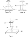
- Figure 7A shows a Gaussian beam intensity profile that generally occurs when a laser beam is brought to a focus and Figure 7B shows a beam profile provided at the surface of the TC layer according to an embodiment of the invention.
- Figure 7A plots the power density or energy density distribution that arises at the focal plane when a pulsed laser beam is focussed with a lens.
- Gaussian distribution which has a peak power or energy density in the centre reducing to low values at the edges.
- Such a highly non-uniform beam profile is undesirable for two reasons: energy below the ablation threshold (Eabl) of the TC material is deposited as heat in the area around the focal spot causing thermal damage to the TC layer and the underlying layers and the peak energy density in the centre of the beam is well above the ablation threshold so significant energy can penetrate the TC layer causing damage to the layers below.
- ablation threshold Eabl
- Figure 7B shows the energy density distribution provided at the surface of the TC layer according to the first embodiment of this invention.
- a so called “top hat” distribution of power or energy density is used where most of the energy in the laser pulse is contained in a region above the ablation threshold energy density (Eabl).
- the distribution would be truly top hat with no significant peak at the centre of the beam but, in practice, this is difficult to achieve so some variation in energy density over a range Emin to Emax is acceptable.
- Emax does not exceed 1.3 x Eabl, where Eabl is the threshold energy density for ablation of the TC layer.
- Figure 8 shows one way of creating a top hat energy density distribution in the laser spot at the surface of the TC layer.
- Aperture 22 is placed in the laser beam 20 and lens 23 forms an image 24 of the aperture on the surface of the substrate 25 coated supporting the CF/BM, OP and TC layers. If the diameter of the aperture is substantially less than the diameter of the beam irradiating it then the low energy density portion of the beam will be removed and a beam profile of the type shown in Figure 7B formed on the TC layer surface. Since the incident laser beam is generally round it is usual to use circular apertures and hence create circular spots on the TC surface.
- Figure 9 shows another way of creating a top hat energy density distribution in the laser spot at the surface of the TC layer.
- Diffractive optical element (DOE) 26 situated in the laser beam 20 is designed such that it forms a top hat energy density distribution at the focal plane 27 of lens 23 which is located on the CF substrate 25.
- DOE diffractive optical element
- Figure 10 shows a schematic perspective view of one form of apparatus arranged to carry out the laser patterning process described above.
- Laser 28 emits laser beam 20 which is directed via mirrors 29, 29' to a two-dimensional scanner unit 30.
- the beam exiting the scanner is focussed by an f-theta lens 31 onto the surface of a substrate 25 which is mounted on stages such that it can be moved in directions X and Y.
- the substrate 25 is coated with an RGB CF layer, an organic layer and a top TC layer (as described above). With the substrate 25 stationary, the scanner 30 moves the beam over sub-areas 32 of the substrate 25 forming isolating grooves in the TC layer required to form the touch sensor electrode structure.
- Sub areas 32 can correspond to complete touch sensors for small devices (such as smart phones) or may form only part of larger touch sensors for larger devices (such as tablets and PCs). In the latter case, the sub-areas need to be 'stitched' together to form the electrode structure of the touch sensor.
- control means such as a computer, which is arranged to control the laser and movement of the laser to carry out the scanning processes described.
- the capacitive touch sensor laser patterning process described above can be performed on substrates which each contain one or more CF devices that are subsequently aligned to and attached to LCDs or, alternatively, the laser patterning can be performed on individual devices.
- Figure 11 shows how devices (e.g. an aperture or DOE) can be inserted into the laser beam path 20 to form a top hat energy distribution at the substrate.
- Pulsed laser 28 emits beam 20 which is deflected in 2 axes by scanner unit 30 and focussed by lens 31 onto the substrate 25.
- Aperture 22 is generally placed in the beam at some distance from lens 31 since the image of the aperture at the substrate is generally highly reduced in size so that the distance from lens 31 to the aperture 22 must be much longer than the distance from the lens 31 to the substrate 25.
- a DOE 26 is used instead of an aperture to form the top hat beam profile then it is generally placed close to the lens 31 which in practice means just before scanner unit 30.
- Such a process differs from known processes for forming electrode structures of a touch sensor.
- laser scribing has significant advantages over known lithographic methods. It is much more efficient: it can be carried out more quickly, it has a much better yield than a lithographic process and it can be adapted more easily. The above process thus provides considerable advantage over known lithographic methods for forming the electrode structures of an in-cell touch sensor.
- the transparent conductive layer is provided on a glass layer (or other layer which absorbs some of the laser energy).
- the method may not need to use a laser beam with a top-hat profile to avoid damaging the underlying layers as the glass layer provides some protection for the underlying layers.
- Such a method is described in GB 2511064 A .
Landscapes
- Engineering & Computer Science (AREA)
- Physics & Mathematics (AREA)
- Optics & Photonics (AREA)
- Plasma & Fusion (AREA)
- Mechanical Engineering (AREA)
- General Engineering & Computer Science (AREA)
- Theoretical Computer Science (AREA)
- Human Computer Interaction (AREA)
- General Physics & Mathematics (AREA)
- Laser Beam Processing (AREA)
Applications Claiming Priority (2)
| Application Number | Priority Date | Filing Date | Title |
|---|---|---|---|
| GB1303085.3A GB2514084B (en) | 2013-02-21 | 2013-02-21 | Method of forming an electrode structure for capacitive touch sensor |
| PCT/GB2014/050439 WO2014128440A1 (en) | 2013-02-21 | 2014-02-14 | Method for forming an electrode structure for a capacitive touch sensor |
Publications (2)
| Publication Number | Publication Date |
|---|---|
| EP2958704A1 EP2958704A1 (en) | 2015-12-30 |
| EP2958704B1 true EP2958704B1 (en) | 2019-11-06 |
Family
ID=48091874
Family Applications (1)
| Application Number | Title | Priority Date | Filing Date |
|---|---|---|---|
| EP14705404.3A Active EP2958704B1 (en) | 2013-02-21 | 2014-02-14 | Method for forming an electrode structure for a capacitive touch sensor |
Country Status (8)
| Country | Link |
|---|---|
| US (1) | US10203817B2 (ja) |
| EP (1) | EP2958704B1 (ja) |
| JP (1) | JP6445465B2 (ja) |
| KR (1) | KR20150120392A (ja) |
| CN (1) | CN105073332B (ja) |
| GB (1) | GB2514084B (ja) |
| TW (1) | TWI656933B (ja) |
| WO (1) | WO2014128440A1 (ja) |
Families Citing this family (4)
| Publication number | Priority date | Publication date | Assignee | Title |
|---|---|---|---|---|
| US10814493B2 (en) * | 2017-01-12 | 2020-10-27 | Robotiq Inc. | Tactile sensor and a method of manufacturing thereof |
| GB201803723D0 (en) * | 2018-03-08 | 2018-04-25 | M Solv Ltd | Method of manufacturing a touch sensitive panel |
| US20200133018A1 (en) * | 2018-10-24 | 2020-04-30 | Himax Technologies Limited | Diffractive optical element module |
| CN114178710A (zh) * | 2020-08-24 | 2022-03-15 | 奥特斯(中国)有限公司 | 部件承载件及其制造方法 |
Family Cites Families (38)
| Publication number | Priority date | Publication date | Assignee | Title |
|---|---|---|---|---|
| JP3371304B2 (ja) * | 1994-07-25 | 2003-01-27 | セイコーエプソン株式会社 | レーザ加工装置及びレーザ加工方法並びに液晶パネル |
| JP3997450B2 (ja) | 1998-03-13 | 2007-10-24 | ソニー株式会社 | 波長変換装置 |
| GB2397545B (en) * | 2002-01-11 | 2005-05-11 | Electro Scient Ind Inc | Method for laser machining a workpiece with laser spot enlargement |
| US6706998B2 (en) | 2002-01-11 | 2004-03-16 | Electro Scientific Industries, Inc. | Simulated laser spot enlargement |
| JP2004344928A (ja) * | 2003-05-22 | 2004-12-09 | Alps Electric Co Ltd | 反射体製造装置及び反射体の製造方法 |
| US7057135B2 (en) | 2004-03-04 | 2006-06-06 | Matsushita Electric Industrial, Co. Ltd. | Method of precise laser nanomachining with UV ultrafast laser pulses |
| US7804043B2 (en) * | 2004-06-15 | 2010-09-28 | Laserfacturing Inc. | Method and apparatus for dicing of thin and ultra thin semiconductor wafer using ultrafast pulse laser |
| JP2006123004A (ja) | 2004-09-29 | 2006-05-18 | Mitsubishi Materials Corp | レーザ加工方法及びレーザ加工装置 |
| JP4641172B2 (ja) * | 2004-10-18 | 2011-03-02 | 大日本印刷株式会社 | Ito膜のパターンニング方法 |
| US20060261924A1 (en) * | 2005-05-20 | 2006-11-23 | Swenson Edward J | Method of forming passive electronic components on a substrate by direct write technique using shaped uniform laser beam |
| US9138913B2 (en) * | 2005-09-08 | 2015-09-22 | Imra America, Inc. | Transparent material processing with an ultrashort pulse laser |
| US7605343B2 (en) * | 2006-05-24 | 2009-10-20 | Electro Scientific Industries, Inc. | Micromachining with short-pulsed, solid-state UV laser |
| US8624157B2 (en) * | 2006-05-25 | 2014-01-07 | Electro Scientific Industries, Inc. | Ultrashort laser pulse wafer scribing |
| JP4299326B2 (ja) * | 2006-08-30 | 2009-07-22 | アルプス電気株式会社 | 入力装置及びその製造方法 |
| JP4752033B2 (ja) | 2006-09-29 | 2011-08-17 | グンゼ株式会社 | タッチパネル及びタッチパネルの製造方法 |
| JP4866778B2 (ja) | 2007-04-24 | 2012-02-01 | 住友重機械工業株式会社 | ビーム照射装置、及び、ビーム照射方法 |
| JP4914309B2 (ja) | 2007-08-24 | 2012-04-11 | グンゼ株式会社 | 基板製造方法及び基板を用いた静電容量式タッチパネル |
| TWI393924B (zh) | 2008-06-25 | 2013-04-21 | Au Optronics Corp | 觸控式顯示面板、彩色濾光片及其製作方法 |
| CN201380363Y (zh) * | 2008-12-30 | 2010-01-13 | 武汉楚天激光(集团)股份有限公司 | 用于激光刻膜的激光设备 |
| GB0900036D0 (en) * | 2009-01-03 | 2009-02-11 | M Solv Ltd | Method and apparatus for forming grooves with complex shape in the surface of apolymer |
| WO2010093779A1 (en) | 2009-02-12 | 2010-08-19 | Optera, Inc. | Plastic capacitive touch screen and method of manufacturing same |
| GB2472613B (en) | 2009-08-11 | 2015-06-03 | M Solv Ltd | Capacitive touch panels |
| CN201645056U (zh) * | 2009-09-28 | 2010-11-24 | 深圳市大族激光科技股份有限公司 | 激光加工装置 |
| TW201142418A (en) | 2010-05-20 | 2011-12-01 | Unidisplay Inc | Touch-sensing display panel and color filter touch-sensing substrate |
| US20120074109A1 (en) * | 2010-09-29 | 2012-03-29 | General Electric Company | Method and system for scribing a multilayer panel |
| KR20120050169A (ko) | 2010-11-10 | 2012-05-18 | 삼성전기주식회사 | 터치패널 및 그 제조방법 |
| JP2012123744A (ja) * | 2010-12-10 | 2012-06-28 | Shin Etsu Polymer Co Ltd | 静電容量式入力装置およびその製造方法、静電容量式入力装置の入力方法 |
| TW201229616A (en) * | 2011-01-07 | 2012-07-16 | Unidisplay Inc | Touch panel |
| GB2487962B (en) * | 2011-02-11 | 2016-10-12 | M-Solv Ltd | Method for making a two-layer capacitive touch sensor panel |
| JP2012174578A (ja) | 2011-02-23 | 2012-09-10 | Gunze Ltd | 透明電極フィルムおよび透明タッチパネル |
| US8648277B2 (en) | 2011-03-31 | 2014-02-11 | Electro Scientific Industries, Inc. | Laser direct ablation with picosecond laser pulses at high pulse repetition frequencies |
| CN102759863B (zh) | 2011-04-27 | 2015-12-02 | 瑞世达科技(厦门)有限公司 | 激光光刻机 |
| US9029242B2 (en) * | 2011-06-15 | 2015-05-12 | Applied Materials, Inc. | Damage isolation by shaped beam delivery in laser scribing process |
| US8635887B2 (en) * | 2011-08-10 | 2014-01-28 | Corning Incorporated | Methods for separating glass substrate sheets by laser-formed grooves |
| US9312855B2 (en) * | 2012-01-10 | 2016-04-12 | Atmel Corporation | Touch sensor tracks |
| US8652940B2 (en) * | 2012-04-10 | 2014-02-18 | Applied Materials, Inc. | Wafer dicing used hybrid multi-step laser scribing process with plasma etch |
| CN202736018U (zh) | 2012-09-14 | 2013-02-13 | 深圳市鹏扬达数码科技有限公司 | 高灵敏度大尺寸电容式内嵌触摸屏 |
| GB2511064A (en) | 2013-02-21 | 2014-08-27 | M Solv Ltd | Method of forming electrode structure for capacitive touch sensor |
-
2013
- 2013-02-21 GB GB1303085.3A patent/GB2514084B/en not_active Expired - Fee Related
-
2014
- 2014-02-14 WO PCT/GB2014/050439 patent/WO2014128440A1/en active Application Filing
- 2014-02-14 CN CN201480009362.5A patent/CN105073332B/zh active Active
- 2014-02-14 EP EP14705404.3A patent/EP2958704B1/en active Active
- 2014-02-14 US US14/769,431 patent/US10203817B2/en not_active Expired - Fee Related
- 2014-02-14 JP JP2015558541A patent/JP6445465B2/ja not_active Expired - Fee Related
- 2014-02-14 KR KR1020157023435A patent/KR20150120392A/ko active IP Right Grant
- 2014-02-21 TW TW103105944A patent/TWI656933B/zh not_active IP Right Cessation
Non-Patent Citations (1)
| Title |
|---|
| None * |
Also Published As
| Publication number | Publication date |
|---|---|
| WO2014128440A1 (en) | 2014-08-28 |
| CN105073332B (zh) | 2018-05-04 |
| TWI656933B (zh) | 2019-04-21 |
| GB2514084B (en) | 2016-07-27 |
| CN105073332A (zh) | 2015-11-18 |
| WO2014128440A4 (en) | 2014-10-09 |
| US20160004349A1 (en) | 2016-01-07 |
| US10203817B2 (en) | 2019-02-12 |
| GB2514084A (en) | 2014-11-19 |
| TW201501849A (zh) | 2015-01-16 |
| GB201303085D0 (en) | 2013-04-10 |
| JP2016516226A (ja) | 2016-06-02 |
| KR20150120392A (ko) | 2015-10-27 |
| EP2958704A1 (en) | 2015-12-30 |
| JP6445465B2 (ja) | 2018-12-26 |
Similar Documents
| Publication | Publication Date | Title |
|---|---|---|
| EP2958705B1 (en) | Method for forming an electrode structure for a capacitive touch sensor | |
| US20170197868A1 (en) | Laser Processing of Electronic Device Structures | |
| US10303038B2 (en) | Beam steering apparatus and system including the same | |
| EP2958704B1 (en) | Method for forming an electrode structure for a capacitive touch sensor | |
| CN102725096B (zh) | 激光加工方法 | |
| CN1178100C (zh) | 反射器和液晶显示器的制造方法 | |
| US8673104B2 (en) | Fabricating method of liquid crystal display device | |
| US20210138577A1 (en) | Using lasers to reduce reflection of transparent solids, coatings and devices employing transparent solids | |
| JP2008216958A (ja) | 絶縁体からなるマザー基板(絶縁マザー基板)にアラインマークを形成することを含む液晶表示装置の製造方法。 | |
| JP2016518252A5 (ja) | ||
| CN103878492A (zh) | 用于修剪显示器中的偏光器的方法与装备 | |
| KR20120018701A (ko) | 레이저 리프트오프 방법 및 레이저 리프트오프 장치 | |
| KR20170039296A (ko) | 투명한 기판의 대향하는 제 1 표면 및 제 2 표면 각각에 데포지션된 투명한 제 1 도전 레이어 및 제 2 도전 레이어를 레이저 스크라이빙하는 방법 | |
| JP2016516226A5 (ja) | ||
| GB2506347B (en) | Method for Forming an Electrode Structure for a Capacitive Touch Sensor | |
| Harrison et al. | A study of stitch line formation during high speed laser patterning of thin film indium tin oxide transparent electrodes | |
| KR20170133313A (ko) | 투명 도전막이 형성된 기판 | |
| GB2489940A (en) | Reflective pixel element for reflective display devices | |
| KR101477005B1 (ko) | Full HD급 고해상도 모바일 능동형 유기 자체 발광 소자의 비열 리페어 방법 및 장치 | |
| JP2008180962A (ja) | 液晶パネルのレーザリペア方法、レーザリペア装置及び液晶パネルの製造方法 |
Legal Events
| Date | Code | Title | Description |
|---|---|---|---|
| PUAI | Public reference made under article 153(3) epc to a published international application that has entered the european phase |
Free format text: ORIGINAL CODE: 0009012 |
|
| 17P | Request for examination filed |
Effective date: 20150805 |
|
| AK | Designated contracting states |
Kind code of ref document: A1 Designated state(s): AL AT BE BG CH CY CZ DE DK EE ES FI FR GB GR HR HU IE IS IT LI LT LU LV MC MK MT NL NO PL PT RO RS SE SI SK SM TR |
|
| AX | Request for extension of the european patent |
Extension state: BA ME |
|
| DAX | Request for extension of the european patent (deleted) | ||
| STAA | Information on the status of an ep patent application or granted ep patent |
Free format text: STATUS: EXAMINATION IS IN PROGRESS |
|
| 17Q | First examination report despatched |
Effective date: 20180329 |
|
| REG | Reference to a national code |
Ref country code: DE Ref legal event code: R079 Ref document number: 602014056235 Country of ref document: DE Free format text: PREVIOUS MAIN CLASS: B23K0026360000 Ipc: B23K0026364000 |
|
| RIC1 | Information provided on ipc code assigned before grant |
Ipc: B23K 26/066 20140101ALI20190625BHEP Ipc: B23K 103/00 20060101ALI20190625BHEP Ipc: B23K 26/40 20140101ALI20190625BHEP Ipc: B23K 26/364 20140101AFI20190625BHEP Ipc: B23K 26/0622 20140101ALI20190625BHEP |
|
| GRAP | Despatch of communication of intention to grant a patent |
Free format text: ORIGINAL CODE: EPIDOSNIGR1 |
|
| STAA | Information on the status of an ep patent application or granted ep patent |
Free format text: STATUS: GRANT OF PATENT IS INTENDED |
|
| INTG | Intention to grant announced |
Effective date: 20190819 |
|
| GRAS | Grant fee paid |
Free format text: ORIGINAL CODE: EPIDOSNIGR3 |
|
| GRAA | (expected) grant |
Free format text: ORIGINAL CODE: 0009210 |
|
| STAA | Information on the status of an ep patent application or granted ep patent |
Free format text: STATUS: THE PATENT HAS BEEN GRANTED |
|
| AK | Designated contracting states |
Kind code of ref document: B1 Designated state(s): AL AT BE BG CH CY CZ DE DK EE ES FI FR GB GR HR HU IE IS IT LI LT LU LV MC MK MT NL NO PL PT RO RS SE SI SK SM TR |
|
| REG | Reference to a national code |
Ref country code: GB Ref legal event code: FG4D |
|
| REG | Reference to a national code |
Ref country code: AT Ref legal event code: REF Ref document number: 1198100 Country of ref document: AT Kind code of ref document: T Effective date: 20191115 Ref country code: CH Ref legal event code: EP |
|
| REG | Reference to a national code |
Ref country code: DE Ref legal event code: R096 Ref document number: 602014056235 Country of ref document: DE |
|
| REG | Reference to a national code |
Ref country code: IE Ref legal event code: FG4D |
|
| REG | Reference to a national code |
Ref country code: NL Ref legal event code: MP Effective date: 20191106 |
|
| REG | Reference to a national code |
Ref country code: LT Ref legal event code: MG4D |
|
| PG25 | Lapsed in a contracting state [announced via postgrant information from national office to epo] |
Ref country code: FI Free format text: LAPSE BECAUSE OF FAILURE TO SUBMIT A TRANSLATION OF THE DESCRIPTION OR TO PAY THE FEE WITHIN THE PRESCRIBED TIME-LIMIT Effective date: 20191106 Ref country code: BG Free format text: LAPSE BECAUSE OF FAILURE TO SUBMIT A TRANSLATION OF THE DESCRIPTION OR TO PAY THE FEE WITHIN THE PRESCRIBED TIME-LIMIT Effective date: 20200206 Ref country code: PL Free format text: LAPSE BECAUSE OF FAILURE TO SUBMIT A TRANSLATION OF THE DESCRIPTION OR TO PAY THE FEE WITHIN THE PRESCRIBED TIME-LIMIT Effective date: 20191106 Ref country code: LV Free format text: LAPSE BECAUSE OF FAILURE TO SUBMIT A TRANSLATION OF THE DESCRIPTION OR TO PAY THE FEE WITHIN THE PRESCRIBED TIME-LIMIT Effective date: 20191106 Ref country code: NL Free format text: LAPSE BECAUSE OF FAILURE TO SUBMIT A TRANSLATION OF THE DESCRIPTION OR TO PAY THE FEE WITHIN THE PRESCRIBED TIME-LIMIT Effective date: 20191106 Ref country code: SE Free format text: LAPSE BECAUSE OF FAILURE TO SUBMIT A TRANSLATION OF THE DESCRIPTION OR TO PAY THE FEE WITHIN THE PRESCRIBED TIME-LIMIT Effective date: 20191106 Ref country code: LT Free format text: LAPSE BECAUSE OF FAILURE TO SUBMIT A TRANSLATION OF THE DESCRIPTION OR TO PAY THE FEE WITHIN THE PRESCRIBED TIME-LIMIT Effective date: 20191106 Ref country code: GR Free format text: LAPSE BECAUSE OF FAILURE TO SUBMIT A TRANSLATION OF THE DESCRIPTION OR TO PAY THE FEE WITHIN THE PRESCRIBED TIME-LIMIT Effective date: 20200207 Ref country code: NO Free format text: LAPSE BECAUSE OF FAILURE TO SUBMIT A TRANSLATION OF THE DESCRIPTION OR TO PAY THE FEE WITHIN THE PRESCRIBED TIME-LIMIT Effective date: 20200206 Ref country code: PT Free format text: LAPSE BECAUSE OF FAILURE TO SUBMIT A TRANSLATION OF THE DESCRIPTION OR TO PAY THE FEE WITHIN THE PRESCRIBED TIME-LIMIT Effective date: 20200306 |
|
| PGFP | Annual fee paid to national office [announced via postgrant information from national office to epo] |
Ref country code: GB Payment date: 20200206 Year of fee payment: 7 Ref country code: DE Payment date: 20200204 Year of fee payment: 7 |
|
| PG25 | Lapsed in a contracting state [announced via postgrant information from national office to epo] |
Ref country code: IS Free format text: LAPSE BECAUSE OF FAILURE TO SUBMIT A TRANSLATION OF THE DESCRIPTION OR TO PAY THE FEE WITHIN THE PRESCRIBED TIME-LIMIT Effective date: 20200306 Ref country code: RS Free format text: LAPSE BECAUSE OF FAILURE TO SUBMIT A TRANSLATION OF THE DESCRIPTION OR TO PAY THE FEE WITHIN THE PRESCRIBED TIME-LIMIT Effective date: 20191106 Ref country code: HR Free format text: LAPSE BECAUSE OF FAILURE TO SUBMIT A TRANSLATION OF THE DESCRIPTION OR TO PAY THE FEE WITHIN THE PRESCRIBED TIME-LIMIT Effective date: 20191106 |
|
| PG25 | Lapsed in a contracting state [announced via postgrant information from national office to epo] |
Ref country code: AL Free format text: LAPSE BECAUSE OF FAILURE TO SUBMIT A TRANSLATION OF THE DESCRIPTION OR TO PAY THE FEE WITHIN THE PRESCRIBED TIME-LIMIT Effective date: 20191106 |
|
| PGFP | Annual fee paid to national office [announced via postgrant information from national office to epo] |
Ref country code: FR Payment date: 20200214 Year of fee payment: 7 |
|
| PG25 | Lapsed in a contracting state [announced via postgrant information from national office to epo] |
Ref country code: RO Free format text: LAPSE BECAUSE OF FAILURE TO SUBMIT A TRANSLATION OF THE DESCRIPTION OR TO PAY THE FEE WITHIN THE PRESCRIBED TIME-LIMIT Effective date: 20191106 Ref country code: ES Free format text: LAPSE BECAUSE OF FAILURE TO SUBMIT A TRANSLATION OF THE DESCRIPTION OR TO PAY THE FEE WITHIN THE PRESCRIBED TIME-LIMIT Effective date: 20191106 Ref country code: CZ Free format text: LAPSE BECAUSE OF FAILURE TO SUBMIT A TRANSLATION OF THE DESCRIPTION OR TO PAY THE FEE WITHIN THE PRESCRIBED TIME-LIMIT Effective date: 20191106 Ref country code: EE Free format text: LAPSE BECAUSE OF FAILURE TO SUBMIT A TRANSLATION OF THE DESCRIPTION OR TO PAY THE FEE WITHIN THE PRESCRIBED TIME-LIMIT Effective date: 20191106 Ref country code: DK Free format text: LAPSE BECAUSE OF FAILURE TO SUBMIT A TRANSLATION OF THE DESCRIPTION OR TO PAY THE FEE WITHIN THE PRESCRIBED TIME-LIMIT Effective date: 20191106 |
|
| REG | Reference to a national code |
Ref country code: DE Ref legal event code: R097 Ref document number: 602014056235 Country of ref document: DE |
|
| REG | Reference to a national code |
Ref country code: AT Ref legal event code: MK05 Ref document number: 1198100 Country of ref document: AT Kind code of ref document: T Effective date: 20191106 |
|
| PG25 | Lapsed in a contracting state [announced via postgrant information from national office to epo] |
Ref country code: SM Free format text: LAPSE BECAUSE OF FAILURE TO SUBMIT A TRANSLATION OF THE DESCRIPTION OR TO PAY THE FEE WITHIN THE PRESCRIBED TIME-LIMIT Effective date: 20191106 Ref country code: SK Free format text: LAPSE BECAUSE OF FAILURE TO SUBMIT A TRANSLATION OF THE DESCRIPTION OR TO PAY THE FEE WITHIN THE PRESCRIBED TIME-LIMIT Effective date: 20191106 |
|
| PLBE | No opposition filed within time limit |
Free format text: ORIGINAL CODE: 0009261 |
|
| STAA | Information on the status of an ep patent application or granted ep patent |
Free format text: STATUS: NO OPPOSITION FILED WITHIN TIME LIMIT |
|
| REG | Reference to a national code |
Ref country code: CH Ref legal event code: PL |
|
| 26N | No opposition filed |
Effective date: 20200807 |
|
| REG | Reference to a national code |
Ref country code: BE Ref legal event code: MM Effective date: 20200229 |
|
| PG25 | Lapsed in a contracting state [announced via postgrant information from national office to epo] |
Ref country code: LU Free format text: LAPSE BECAUSE OF NON-PAYMENT OF DUE FEES Effective date: 20200214 Ref country code: MC Free format text: LAPSE BECAUSE OF FAILURE TO SUBMIT A TRANSLATION OF THE DESCRIPTION OR TO PAY THE FEE WITHIN THE PRESCRIBED TIME-LIMIT Effective date: 20191106 |
|
| PG25 | Lapsed in a contracting state [announced via postgrant information from national office to epo] |
Ref country code: AT Free format text: LAPSE BECAUSE OF FAILURE TO SUBMIT A TRANSLATION OF THE DESCRIPTION OR TO PAY THE FEE WITHIN THE PRESCRIBED TIME-LIMIT Effective date: 20191106 Ref country code: CH Free format text: LAPSE BECAUSE OF NON-PAYMENT OF DUE FEES Effective date: 20200229 Ref country code: SI Free format text: LAPSE BECAUSE OF FAILURE TO SUBMIT A TRANSLATION OF THE DESCRIPTION OR TO PAY THE FEE WITHIN THE PRESCRIBED TIME-LIMIT Effective date: 20191106 Ref country code: LI Free format text: LAPSE BECAUSE OF NON-PAYMENT OF DUE FEES Effective date: 20200229 |
|
| PG25 | Lapsed in a contracting state [announced via postgrant information from national office to epo] |
Ref country code: IT Free format text: LAPSE BECAUSE OF FAILURE TO SUBMIT A TRANSLATION OF THE DESCRIPTION OR TO PAY THE FEE WITHIN THE PRESCRIBED TIME-LIMIT Effective date: 20191106 Ref country code: IE Free format text: LAPSE BECAUSE OF NON-PAYMENT OF DUE FEES Effective date: 20200214 |
|
| PG25 | Lapsed in a contracting state [announced via postgrant information from national office to epo] |
Ref country code: BE Free format text: LAPSE BECAUSE OF NON-PAYMENT OF DUE FEES Effective date: 20200229 |
|
| REG | Reference to a national code |
Ref country code: DE Ref legal event code: R119 Ref document number: 602014056235 Country of ref document: DE |
|
| GBPC | Gb: european patent ceased through non-payment of renewal fee |
Effective date: 20210214 |
|
| PG25 | Lapsed in a contracting state [announced via postgrant information from national office to epo] |
Ref country code: DE Free format text: LAPSE BECAUSE OF NON-PAYMENT OF DUE FEES Effective date: 20210901 Ref country code: GB Free format text: LAPSE BECAUSE OF NON-PAYMENT OF DUE FEES Effective date: 20210214 Ref country code: FR Free format text: LAPSE BECAUSE OF NON-PAYMENT OF DUE FEES Effective date: 20210228 |
|
| PG25 | Lapsed in a contracting state [announced via postgrant information from national office to epo] |
Ref country code: TR Free format text: LAPSE BECAUSE OF FAILURE TO SUBMIT A TRANSLATION OF THE DESCRIPTION OR TO PAY THE FEE WITHIN THE PRESCRIBED TIME-LIMIT Effective date: 20191106 Ref country code: MT Free format text: LAPSE BECAUSE OF FAILURE TO SUBMIT A TRANSLATION OF THE DESCRIPTION OR TO PAY THE FEE WITHIN THE PRESCRIBED TIME-LIMIT Effective date: 20191106 Ref country code: CY Free format text: LAPSE BECAUSE OF FAILURE TO SUBMIT A TRANSLATION OF THE DESCRIPTION OR TO PAY THE FEE WITHIN THE PRESCRIBED TIME-LIMIT Effective date: 20191106 |
|
| PG25 | Lapsed in a contracting state [announced via postgrant information from national office to epo] |
Ref country code: MK Free format text: LAPSE BECAUSE OF FAILURE TO SUBMIT A TRANSLATION OF THE DESCRIPTION OR TO PAY THE FEE WITHIN THE PRESCRIBED TIME-LIMIT Effective date: 20191106 |