EP2950108A1 - Dispositifs de détection de tension sans contact - Google Patents
Dispositifs de détection de tension sans contact Download PDFInfo
- Publication number
- EP2950108A1 EP2950108A1 EP15166827.4A EP15166827A EP2950108A1 EP 2950108 A1 EP2950108 A1 EP 2950108A1 EP 15166827 A EP15166827 A EP 15166827A EP 2950108 A1 EP2950108 A1 EP 2950108A1
- Authority
- EP
- European Patent Office
- Prior art keywords
- voltage sensing
- impedance
- sensing device
- contactless voltage
- antenna
- Prior art date
- Legal status (The legal status is an assumption and is not a legal conclusion. Google has not performed a legal analysis and makes no representation as to the accuracy of the status listed.)
- Granted
Links
- 230000003071 parasitic effect Effects 0.000 claims abstract description 68
- 239000004020 conductor Substances 0.000 claims abstract description 61
- 238000005259 measurement Methods 0.000 claims abstract description 43
- 238000004891 communication Methods 0.000 claims abstract description 29
- 238000012544 monitoring process Methods 0.000 claims description 57
- 239000000615 nonconductor Substances 0.000 claims description 17
- 238000010295 mobile communication Methods 0.000 claims description 4
- 230000005611 electricity Effects 0.000 description 38
- 239000003990 capacitor Substances 0.000 description 22
- 230000003287 optical effect Effects 0.000 description 6
- 238000009434 installation Methods 0.000 description 5
- 230000015572 biosynthetic process Effects 0.000 description 4
- 238000000034 method Methods 0.000 description 4
- 230000002411 adverse Effects 0.000 description 3
- 230000005670 electromagnetic radiation Effects 0.000 description 3
- 239000002184 metal Substances 0.000 description 3
- 238000012545 processing Methods 0.000 description 3
- 230000001681 protective effect Effects 0.000 description 3
- 230000003831 deregulation Effects 0.000 description 2
- 238000012986 modification Methods 0.000 description 2
- 230000004048 modification Effects 0.000 description 2
- 230000008569 process Effects 0.000 description 2
- 230000008439 repair process Effects 0.000 description 2
- 230000035945 sensitivity Effects 0.000 description 2
- 230000009471 action Effects 0.000 description 1
- 230000005540 biological transmission Effects 0.000 description 1
- 239000002419 bulk glass Substances 0.000 description 1
- 239000000919 ceramic Substances 0.000 description 1
- 229920001940 conductive polymer Polymers 0.000 description 1
- 238000010276 construction Methods 0.000 description 1
- 238000013461 design Methods 0.000 description 1
- 230000000694 effects Effects 0.000 description 1
- 230000005684 electric field Effects 0.000 description 1
- 230000007613 environmental effect Effects 0.000 description 1
- 239000000835 fiber Substances 0.000 description 1
- 239000012811 non-conductive material Substances 0.000 description 1
- 230000009467 reduction Effects 0.000 description 1
- 239000010979 ruby Substances 0.000 description 1
- 229910001750 ruby Inorganic materials 0.000 description 1
- 238000000926 separation method Methods 0.000 description 1
Images


Classifications
-
- G—PHYSICS
- G01—MEASURING; TESTING
- G01R—MEASURING ELECTRIC VARIABLES; MEASURING MAGNETIC VARIABLES
- G01R19/00—Arrangements for measuring currents or voltages or for indicating presence or sign thereof
- G01R19/0084—Arrangements for measuring currents or voltages or for indicating presence or sign thereof measuring voltage only
-
- G—PHYSICS
- G01—MEASURING; TESTING
- G01R—MEASURING ELECTRIC VARIABLES; MEASURING MAGNETIC VARIABLES
- G01R15/00—Details of measuring arrangements of the types provided for in groups G01R17/00 - G01R29/00, G01R33/00 - G01R33/26 or G01R35/00
- G01R15/04—Voltage dividers
- G01R15/06—Voltage dividers having reactive components, e.g. capacitive transformer
-
- G—PHYSICS
- G01—MEASURING; TESTING
- G01R—MEASURING ELECTRIC VARIABLES; MEASURING MAGNETIC VARIABLES
- G01R15/00—Details of measuring arrangements of the types provided for in groups G01R17/00 - G01R29/00, G01R33/00 - G01R33/26 or G01R35/00
- G01R15/14—Adaptations providing voltage or current isolation, e.g. for high-voltage or high-current networks
- G01R15/16—Adaptations providing voltage or current isolation, e.g. for high-voltage or high-current networks using capacitive devices
Definitions
- Embodiments of the present specification relate to sensing devices, and more particularly to voltage sensing devices.
- electricity providers may be able to significantly reduce the amount of electricity lost in the electricity networks and make considerable savings in the cost of generating the electricity. Furthermore, by closely monitoring the electricity networks electricity providers will be in a better position to correct faults in the electricity networks swiftly with a minimum of inconvenience to their customers, thereby providing an improved quality of supply to their customers.
- a variety of sensors have been developed for measuring a current in a current carrying cable, such as a current carrying cable in a high voltage electricity distribution system.
- optical current sensors are used to measure the current in the current carrying cable.
- the optical current sensors are generally based on the Faraday effect.
- Some optical current sensors use bulk glass or fiber optic cables that surround the current carrying cable.
- the optical current sensors have a very high dynamic range, however, the optical current sensors require opening the current carrying cable at installation, which may be an expensive procedure.
- Other kind of sensors that are used for measuring voltages in the electricity networks may employ metal shells disposed around the current carrying cables. These sensors use the metal shells as capacitance dividers between the current carrying cables and a ground underneath. Among other factors, the capacitance between the shells and the current carrying cables depends on the distance between the shells and the current carrying cables. Accordingly, the metal shells may have limited capacitance between the current carrying cables and the shells themselves because of a limit on a gap between the shells and the current carrying cables. Further, due to the limited capacitance, the sensor may be influenced by changes in surrounding conductors, such as measuring circuits.
- an increase in an area of the shell to increase a capacitance between the shells and the current carrying cables typically results in an increase in a parasitic capacitance of the sensor.
- the increased parasitic capacitance makes the sensor relatively more prone to fluctuations in the surrounding conductors.
- the voltage measurement entails physically connecting the voltage measuring device to the voltage line and to the ground.
- This physical connection between the voltage measuring device and the ground is required to prevent monitored values being undesirably affected by the presence of any object that may exist between the ground and the voltage measuring device.
- a passing vehicle, a tree, an animal, or a bird, or any other object intentionally or unintentionally disposed in close vicinity of the ground and/or the voltage measuring device may result in undesirable changes in the measurement values of the voltage measurement device in absence of the physical connection between the voltage measuring device and the ground.
- providing this physical connection between the voltage measuring devices and the ground requires complex installation procedures. For example, such installation procedures are both time consuming and labor intensive resulting in an increase in the cost of installing the voltage measuring device. Further, the physical connection to the ground may need to be maintained and periodically checked.
- a contactless voltage sensing device configured to measure a voltage value of a conductor with respect to a reference surface.
- the contactless voltage sensing device includes a first impedance element having a first impedance, where the first impedance element is configured to be operatively coupled to the conductor.
- the contactless voltage sensing device includes an antenna operatively coupled to the first impedance element and a second impedance element having a second impedance, wherein the second impedance element is formed in part by the antenna and a parasitic impedance element, and where the parasitic impedance element includes a parasitic impedance.
- the contactless voltage sensing device further includes measurement and communication circuitry coupled to the first impedance element and configured to measure the voltage of the conductor.
- a contactless voltage sensing device configured to measure a voltage value of a conductor with respect to a reference surface.
- the contactless voltage sensing device includes a first impedance element having a first impedance, where the first impedance element is configured to be operatively coupled to the conductor.
- the contactless voltage sensing device includes an antenna operatively coupled to the first impedance element and a second impedance element having a second impedance, where the second impedance element is formed in part by the antenna and a parasitic impedance element, and where the parasitic impedance element includes a parasitic impedance.
- the contactless voltage sensing device further includes measurement and communication circuitry coupled to the first impedance element and configured to measure the voltage value of the conductor. Further, the measurement and communication circuitry is coupled to the first impedance element to measure a voltage of the conductor, where the measurement and control circuitry includes a processor, a monitor, a data acquisition communicator (DAC), or combinations thereof.
- measurement and communication circuitry coupled to the first impedance element and configured to measure the voltage value of the conductor. Further, the measurement and communication circuitry is coupled to the first impedance element to measure a voltage of the conductor, where the measurement and control circuitry includes a processor, a monitor, a data acquisition communicator (DAC), or combinations thereof.
- DAC data acquisition communicator
- a monitoring system includes one or more contactless voltage sensing devices configured to measure a voltage value of a conductor with respect to a reference surface. Further, the contactless voltage sensing device includes a first impedance element having a first impedance, where the first impedance element is configured to be operatively coupled to the conductor. Moreover, the contactless voltage sensing device includes an antenna operatively coupled to the first impedance element, a second impedance element having a second impedance, , and measurement and communication circuitry coupled to the first impedance element to measure a voltage of the conductor.
- the second impedance element is formed in part by the antenna and a parasitic impedance element, where the parasitic impedance element includes a parasitic impedance.
- the monitoring system includes a control unit communicatively coupled to the one or more contactless voltage sensing devices, where the control unit is configured to receive data representative of the voltage value of the conductor from the one or more contactless sensing devices.
- Embodiments of the present specification provide a contactless voltage sensing device configured to measure a voltage value of a conductor with respect to a reference surface. Further, the contactless voltage sensing device may be configured to be physically and operatively coupled to the conductor. As used throughout the present specification, the term "conductor" refers to an electrical conductor. In certain embodiments, the contactless voltage sensing device may be configured to sense one or more electrical parameters from the conductor and measure a voltage value of the conductor with respect to the reference surface based on the sensed electrical parameters. In some embodiments, the conductor may be a power line in an electricity network. In some other embodiments, the conductor may be a bus bar. For example, the conductor may be a bus bar that is disposed in an enclosed switch gear.
- the term "contactless” refers to absence of direct physical contact between the contactless voltage sensing device and the reference surface. It may be noted that in some embodiments the reference surface may be a ground, however, in some other embodiments, the reference surface may be any other surface other than the ground, where the reference surface has a known potential, referred to as a "reference potential.” In a particular example, the contactless voltage sensing device of the present specification is not directly physically coupled to the reference surface (for example, the ground) to provide the reference potential.
- the contactless voltage sensing device may be used for monitoring a voltage in the power line of the electricity network.
- the contactless voltage sensing device may be a line mounted device or a pole mounted device.
- the contactless voltage sensing device may be mounted on a power line, such as, but not limited to, a high voltage power line or a medium voltage power line.
- a voltage of the power line on which the contactless voltage sensing device is disposed may be in a range from about 415 Volts to about 440 kilo-Volts, or higher.
- the contactless voltage sensing device may include a first impedance element having a first impedance and a second impedance element having a second impedance.
- the first and second impedances may be used to measure the voltage of the conductor.
- the first impedance element may include one or more resistors, one or more capacitors, one or more inductors, or combinations thereof.
- the contactless voltage sensing device may include a capacitor as the first impedance element. In operation, the first impedance element is configured to sense an electrical parameter, such as the voltage of the conductor.
- the contactless voltage sensing device includes an antenna that is operatively coupled to the first impedance element.
- the antenna is configured to form the second impedance element in conjunction with the parasitic impedance element.
- the second impedance element is formed by the antenna and a parasitic impedance element, where the parasitic impedance element is formed between the antenna and the reference surface.
- An impedance of the second impedance element also referred to as "second impedance” is a combination of an impedance of the parasitic impedance element, also referred to as "parasitic impedance,” and an impedance of the antenna.
- the impedance of the antenna may be negligible compared to the parasitic impedance.
- a value of the second impedance may be substantially similar to a value of the parasitic impedance.
- the second impedance may be substantially a parasitic impedance that appears between the antenna and the reference surface.
- the parasitic impedance may primarily include a parasitic capacitance.
- the contactless voltage sensing device includes measurement and communication circuitry, where the measurement and communication circuitry is configured to measure a voltage of the conductor based on the voltage value sensed across the first impedance element.
- the first impedance element may be disposed between a first node and a second node.
- the antenna may be disposed between another first node and another second node.
- the second node of the first impedance element may be operatively coupled to the first node of the antenna.
- the second node of the first impedance element and the first node of the antenna may be a common node between the first impedance element and the antenna.
- the first node of the first impedance element may be maintained at the same potential as that of the conductor. Maintaining the first node of the first impedance element at the same potential as that of the conductor enables the contactless voltage sensing device to measure the voltage of the conductor by enabling a voltage corresponding to the conductor to appear across the first impedance element.
- the second node of the antenna may be configured to develop a voltage that is different from the voltage of the conductor. The voltage appearing on the second node of the antenna may be caused due to a current flowing through the parasitic impedance element. Consequently, the structure of the contactless voltage sensing device enables the combination of the first and second impedance elements to act as a voltage divider between the conductor and the reference surface.
- the measurement and communication circuitry may be configured to measure this voltage difference appearing across the first impedance element. In some embodiments, the measurement and communication circuitry may be configured to measure the voltage of the conductor based on the values of the first impedance, second impedance and voltage difference appearing across the first impedance element.
- the contactless voltage sensing device includes an electrically conductive element configured to shield the first impedance element from electromagnetic radiation emanating from the conductor, such as a current carrying power line. Further, in some embodiments, the electrically conductive element may be maintained at the same voltage as that of the conductor.
- the antenna may be an electrically conductive body that has a first portion and a second portion. Further, an electrical insulator may be disposed on the first portion of the antenna to prevent electrical shorting of the electrically conductive body of the antenna with the electrically conductive element. Additionally, the second portion of the antenna may be disposed outside the electrical insulator as well as the electrically conductive element. The second portion of the antenna that is disposed outside the electrical insulator as well as the electrically conductive element may be exposed to the reference surface. Further, the second portion of the antenna in conjunction with the reference surface may contribute to formation of the second impedance and/or parasitic impedance. In certain embodiments, dimensions of the second portion of the antenna may be selected to facilitate relatively smaller values of antenna impedance as compared to parasitic impedance. The second portion of the antenna acts as the second node of the antenna.
- the contactless voltage sensing device may be configured to communicate the measured voltage value to a determined location, such as, but not limited to, a control unit, a monitoring unit, a display unit, or combinations thereof. Further, the contactless voltage sensing device may be configured to communicate the measured voltage value using the measurement and communication circuitry. Advantageously, the contactless voltage sensing device may be configured to enable real-time monitoring of the voltage values of the conductor, such as, but not limited to, a power line.
- measurement values of the contactless voltage sensing device are not undesirably or adversely affected by presence or absence of electrically conductive or electrically non-conductive objects that may be intentionally or unintentionally disposed between the contactless voltage sensing device and the reference surface while the contactless voltage sensing device is sensing and measuring the voltage values of the power line on which it is disposed.
- the measured voltage value of a power line measured by the contactless voltage sensing device may not be adversely affected due to presence of an electrically conducting body, such as, but not limited to, a stationary or moving vehicle in the vicinity of the power line.
- the contactless voltage sensing device is relatively easy to install as compared to conventional measurement devices that require a direct physical connection between the measurement device and the ground.
- the contactless voltage sensing device is configured to be mounted on the power line without any further need of the contactless voltage sensing device being physically coupled to the ground.
- one or more contactless voltage sensing devices may be configured to be employed in a monitoring system, where the monitoring system may include the control unit and/or the monitoring unit.
- the one or more contactless voltage sensing devices may be configured to communicate the measured voltage values of the conductor to the control unit and/or the monitoring unit.
- the one or more contactless voltage sensing devices may include a plurality of data acquisition communicators (DACs).
- the DACs may form part of the measurement and communication circuitry.
- data representative of the voltage of the power line is communicated by a DAC to the control unit, such as the control center computer, over a global system for mobile communication (GSM) link. This is an inexpensive and secure way of sending the data to the control unit, the monitoring unit, or any other control center computer or device.
- GSM global system for mobile communication
- the monitoring system may form part of an electricity network.
- the electrical network may employ one or more monitoring systems.
- the electricity network may employ a plurality of power lines, a plurality of contactless voltage sensing devices, and one or more monitoring systems.
- one or more contactless sensing devices of the plurality of contactless voltage sensing devices may be operatively coupled to one or more monitoring systems.
- the monitoring system may be configured to communicate the measured voltage values to a control unit in the electricity network.
- the contactless voltage sensing devices may be configured to provide signals representative of the voltage value of a corresponding power line of the electricity network over a wide geographical area in a cost effective way.
- each DAC of the plurality of DACs may have one or more contactless voltage sensing devices associated therewith so that the signals representative of the voltage values of the power lines may be transmitted from a contactless voltage sensing device to another contactless voltage sensing device or the control unit of the same or the other monitoring systems.
- the electrical properties transmitted from one DAC to the control unit may be transmitted to another DAC before being transferred to the control unit.
- processing may be carried out either at the DACs or in the control unit.
- the signals may be amplified in the DAC and temporary storage of the data may be carried out in each DAC.
- the contactless voltage sensing device of the present specification may be easily adaptable to different dynamic ranges, bandwidths and sensitivity values.
- the first impedance element may be modified to adapt the contactless voltage sensor for the different dynamic ranges, bandwidths and sensitivity values.
- the first impedance element is a capacitor
- a capacitor with higher capacitance may be used to obtain lower bandwidth, and vice versa.
- a value of the first capacitance of the first impedance element may be equal to or more than about 1 nF.
- a value of the parasitic capacitance from the second impedance element may be less than or equal to about 0.01pF.
- FIG. 1 illustrates an exemplary contactless voltage sensing device 100.
- the contactless voltage sensing device 100 may be configured to measure a voltage value of a conductor, such as, but not limited to, a power line 102 with respect to a reference surface 120.
- the power line 102 may be a high voltage line, a medium voltage line, or any other power line or any other electrical conductor that is configured to carry electrical current.
- the contactless voltage sensing device 100 includes an electrically conductive element in the form of an electrically conductive housing 104.
- the electrically conductive housing 104 may be configured to shield one or more components of the contactless voltage sensing device 100 from electromagnetic radiation of the power line 102.
- the electrically conductive housing 104 may provide shielding to one or more sides of the contactless voltage sensing device 100.
- the electrically conductive housing 104 may be maintained at the same voltage as the power line 102.
- the electrically conductive housing 104 may be shunted to the power line 102 using an electrically conductive connector 106. Maintaining the electrically conductive housing 104 at the same potential as the power line 102 may facilitate reduction in interference otherwise caused due to presence of the electrical field around the electronic components of the contactless voltage sensing device 100. Further, maintaining the electrically conductive housing 104 at the same potential as that of the power line 102 enhances accuracy of measurement of the contactless voltage sensing device 100.
- the contactless voltage sensing device 100 further includes a first impedance element 108 disposed between a first node 107 and a second node 109.
- the first impedance element 108 may include a capacitor, a resistor, an inductor, or combinations thereof. Further, the first impedance element 108 may have an impedance that is referred to as a "first impedance,” hereinafter.
- the first impedance element 108 is configured to sense at least one electrical parameter of the power line 102. By way of example, a voltage appearing across the first impedance element 108 is representative of the sensed electrical parameter of the power line 102.
- the first impedance element 108 is connected to the power line 102 at the first node 107.
- the first impedance element 108 is operatively coupled to an antenna 110 at the second node 109.
- the second node 109 is a common node shared between the first impedance element 108 and the antenna 110.
- the voltage appearing across the first impedance element 108 is representative of the voltage difference that exists between the power line 102 and the second node 109.
- the voltage difference between the power line 102 and the second node 109 is the same as the voltage difference between the electrically conductive housing 104 and the second node 109. Accordingly, the voltage difference across the first impedance element 108 may be measured by disposing a voltage sensing device, such as a voltmeter 112, between nodes 114 and 116.
- the antenna 110 includes a first portion 130 and a second portion 131. It may be noted that the first and second portions 130 and 131 of the antenna 110 may not be physically different entities.
- the first portion 130 of the antenna 110 may be the portion of the antenna 110 that is insulated from the electrically conductive housing 104 using an electrical insulator 128.
- the second portion 131 of the antenna 110 may be the portion that is disposed outside the electrical insulator 128. Further, the second portion 131 of the antenna 110 may be disposed outside the electrically conductive housing 104. Further, the second portion 131 of the antenna 110 may be exposed to the reference surface 120, generally represented by a node 124. In certain embodiments, the node 122 of the antenna 110 is formed on the second portion 131 of the antenna 110.
- the antenna 110 is disposed between the node 109, which is the first node of the antenna 110 and a node 122, which is the second node of the antenna 110. Further, the second portion 131 of the antenna 110 is exposed outside the electrical insulator 128.
- the contactless voltage sensing device 100 includes a second impedance element 133 that is formed by at least a portion of the antenna 110 and a parasitic impedance element 118.
- the second impedance element 133 is formed by the second portion 131 of the antenna 110 and the parasitic impedance element 118.
- the parasitic impedance element 118 is disposed between the antenna 110 and the reference surface 120.
- the parasitic impedance element 118 exists between the node 122 of the antenna 110 and the node 124 representative of the reference surface 120.
- An impedance value of the second impedance element 133 may be referred to as a second impedance.
- the second impedance is a combination of a parasitic impedance and an impedance of the antenna. Further, it may be noted that the second impedance may be substantially similar to the parasitic impedance as a value of the impedance of the antenna may be substantially lower compared to a value of the parasitic impedance.
- the parasitic impedance may be defined as the parasitic capacitance between the antenna 110 and the ground.
- the parasitic capacitance may be defined as an impedance between the antenna 110 and a reference potential, where the reference potential is a potential of the reference surface 120.
- the overall size of the antenna 110 may not matter, however, only the second portion 131 of the antenna that is disposed outside the electrical insulator 128 may contribute to the parasitic impedance.
- a length of the second portion 131 may be up to about 10 cm. Accordingly, it may be desirable to provide the antenna 110 having relatively small dimensions of the second portion 131 to provide relatively high parasitic impedance for the parasitic impedance element. It may be noted that high parasitic impedance or low parasitic capacitance enables the contactless voltage sensing device to be not undesirably influenced by changes in surrounding conductors.
- the antenna 110 may be a cable, a wire, a plate, a patterned elongated structure, an impedance element, or combinations thereof.
- the antenna 110 may include a lumped impedance element.
- the antenna 110 may be a lumped capacitor, where a first terminal of the capacitor is disposed in the electrical insulator 128 and a second terminal of the lumped capacitor is exposed to the reference surface 120.
- the voltage difference (V 1 ) between the nodes 107 and 109 of the first impedance element 108 may appear primarily because of the impedance divider action caused due to the presence of the antenna 110 between the first impedance element 108 and the reference surface 120.
- presence of the antenna 110 results in the formation of the second impedance element 133, thereby providing the divided impedance.
- the antenna impedance is assumed to be negligible compared to the parasitic impedance
- the first impedance element 108 is a capacitor
- the antenna 110 may result in the formation of the parasitic capacitor.
- the first impedance element 108 or the capacitor may act as a voltage divider between the power line 102 and the reference surface 120.
- the second impedance may be at least about 50 times higher than the value of the first impedance. In another embodiment, the second impedance may be at least about 100 times higher than the value of the first impedance. In yet another embodiment, the second impedance is about 100 to 10,000 times higher than the value of the first impedance. In some embodiments, the second impedance may have a relatively high value by virtue of having a high parasitic impedance, a high antenna impedance, or both. In some other embodiments, the second impedance may have a relatively high value by virtue of having a high parasitic impedance.
- the parasitic impedance is primarily governed by the size of the antenna 110. Further, the value of the antenna impedance may be governed by the impedance element used to form the antenna 110. In order to have a relatively low value for the first impedance, in some embodiments, a lumped capacitor may be used as the first impedance element 108.
- the voltage in the power line 102 may be calculated using the value of the first impedance, second impedance, and the voltage difference across the first impedance element 108.
- the voltage value across the first impedance element 108 may be governed by the voltage of the power line 102, however, the value of the second impedance may be governed by the antenna impedance, size of the antenna 110 disposed outside the electrical insulator 128, and the distance between the antenna 110 and the reference surface 120. It is desirable to have minimum variation in the value of the parasitic impedance. Due to the small size of the antenna 110, the value of the parasitic impedance is relatively high. Hence, advantageously, the variation in the estimated value of the voltage (V L ) of the power line 102 is minimized. Accordingly, presence of conductors or other objects between the contactless voltage sensing device 100 and the ground 120 does not adversely affect the measurement of the voltage values in the power line 102.
- the output of the voltmeter 112 may be operatively coupled to measurement and communication circuitry 132.
- the measurement and communication circuitry 132 may include a processor 134, a monitor 136 and a DAC 138.
- the measurement and communication circuitry 132 is configured to measure the voltage difference across the first impedance element 108.
- the processor 134 of the measurement and communication circuitry 132 is configured to determine a voltage value of the power line 102 based on the value of the first impedance, a value of the voltage appearing across the first impedance element 108 and the value of the second impedance.
- a calibration factor may be used to derive actual voltage value of the power line 102 from the measured voltage value.
- the calibration factor may be derived using the voltage drop across the first impedance element 108.
- the determined value of the actual voltage of the power line 102 may be monitored using the monitor. Further, the determined value of the actual voltage of the power line 102 may be wirelessly communicated to other contactless voltage sensing devices (not shown) or a control unit using the DAC 138
- the functions of the processor 134 may be implemented in a variety of programming languages, including but not limited to Ruby, Hypertext Pre-processor (PHP), Perl, Delphi, Python, C, C++, or Java.
- PPP Hypertext Pre-processor
- Such code may be stored or adapted for storage on one or more tangible, machine-readable media, such as on data repository chips, local or remote hard disks, optical disks (that is, CDs or DVDs), solid-state drives, or other media, which may be accessed by the processor-based system to execute the stored code.
- the measurement and communication circuitry 132 may be a high input impedance circuitry.
- the measurement and communication circuitry 132 may be configured to use the values of the first impedance and the parasitic impedance to determine the actual voltage value of the power line 102.
- the measurement and communication circuitry 132 may be disposed in the electrically conductive housing 104. However, in an alternate embodiment not illustrated here, the measurement and communication circuitry 132 may be disposed outside the electrically conductive housing 104.
- the measurement and communication circuitry 132 is communicatively coupled to other devices, such as a control unit (not shown), or other contactless voltage sensing devices using the DAC 138.
- the control unit may be configured to receive data representative of the voltage value of the power line 102 from the one or more contactless sensing devices 100.
- the measurement and communication circuitry 132 may be configured to provide a determined voltage value of the power line 102 to the control unit. In one embodiment, the measurement and communication circuitry 132 may be configured to communicate with the control unit using a DAC 138 or a radio transmitter/receiver.
- the contactless voltage sensing device 100 may be a remote sensing device.
- the term "remote sensing device" may be used to refer to a sensing device that is communicatively coupled to a monitoring unit and/or a control unit while being located in a remote location with respect to the monitoring unit and/or the control unit. In one embodiment, the remote sensing device may be wirelessly coupled to the monitoring unit and/or the control unit.
- the contactless voltage sensing device 100 may include a protective cover or casing that is disposed around at least a portion of the electrically conductive housing 104.
- the protective cover may be made of electrically non-conductive materials, such as but not limited to, electrically non-conductive polymers or electrically non-conductive ceramics. Further, in one embodiment, the protective cover may be configured to provide mechanical strength and/or environmental protection to the contactless voltage sensing device 100.
- FIG. 2 illustrates an alternate embodiment of the contactless voltage sensing device 100 of FIG. 1 .
- the contactless voltage sensing device 200 is operatively coupled to a power line 208 and configured to measure a voltage of the power line 208.
- the contactless voltage sensing device 200 includes a first impedance element 202, an antenna 204 and measurement and communication circuitry 206.
- the contactless voltage sensing device 200 may be configured to be mounted on the power line 208.
- the contactless voltage sensing device 200 may include an electrically conductive element in the form of an electrically conductive shield 210.
- the electrically conductive shield 210 includes a first portion, namely a first electrically conductive shield 212, and a second portion, namely a second electrically shield 214.
- the first electrically conductive shield 212 of the electrically conductive shield 210 is disposed between the first impedance element 202 and the power line 208. Accordingly, the first electrically conductive shield 212 is configured to shield the contactless voltage sensing device 200 from the electromagnetic radiation from the power line 208. Further, the second electrically conductive shield 214 of the electrically conductive shield 210 is disposed between the antenna 204 and a reference surface 216. The second electrically conductive shield 214 is configured to prevent any electrical interference between the reference surface 216 and the first impedance element 202. Further, the second electrically conductive shield 214 may be configured to enable the formation of a second impedance element 225. In particular, the second impedance element 225 may be formed in part by the antenna 204 and a parasitic impedance element 218. Further, the parasitic impedance element 218 may be disposed between the antenna 204 and the reference surface 216.
- the antenna 204 includes a first portion 220, a second portion 224 and an electrical insulator 222.
- the first portion 220 of the antenna 204 may be disposed in the electrical insulator 222, whereas the second portion of the antenna second 204 may be disposed outside the electrical insulator 222.
- the second portion 224 of the antenna 204 may be disposed on the same side of the second electrically conductive shield 214 as the reference surface 216.
- the second portion 224 of the antenna 204 in conjunction with the reference surface 216 may form the parasitic impedance element 218.
- first and second electrically conductive shields 212 and 214 may both be maintained at the same electrical potential as that of the power line 208.
- the electrically conductive shield 210 may include only one of the first or second electrically conductive shields 212 and 214. In one example, the electrically conductive shield 210 may include only the first electrically conductive shield 212.
- FIG. 3 illustrates a contactless voltage sensing device 300 configured to measure a voltage value of a conductor 302 with respect to a reference surface 312.
- the contactless voltage sensing device 300 includes a first impedance element, such as a capacitor 304, an antenna 306 and measurement and communication circuitry 308.
- the measurement and communication circuitry 308 is configured to measure a voltage value based on one or more electrical parameters sensed by the capacitor 304 and a second impedance element 320.
- an antenna impedance is substantially low than a parasitic capacitance. Accordingly, the parasitic capacitance is substantially similar to the second impedance.
- the parasitic capacitance may be sensed across a parasitic capacitor 310 formed between the antenna 306 and the reference surface 312.
- the capacitor 304 is shown as a single or lumped capacitor, however, in an alternative embodiment; a plurality of capacitors may be used to replace the capacitor 304. In some of these embodiments, the plurality of capacitors may be electrically coupled to effectively form a lumped capacitor.
- the antenna 306 may include a portion 314 that is disposed within an electrical insulator 316, and a portion 318 that is disposed outside the electrical insulator 316. The portion 318 disposed outside the electrical insulator 316 forms a parasitic capacitor 310 in conjunction with the reference surface 312.
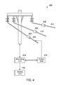
- FIG. 4 illustrates an exemplary embodiment of a monitoring system 400 employed in an electricity network in accordance with aspects of the present specification.
- power lines 408, 410 and 412 may be operatively coupled to a common electric pole to form part of a larger electricity network.
- the monitoring system 400 includes 3 contactless voltage sensing devices 402, 404 and 406 disposed on their respective power lines 408, 410 and 412, respectively.
- the contactless voltage sensing devices 402, 404 and 406 may individually measure the voltages on their respective power lines 408, 410 and 412. Once the voltage values have been measured the contactless voltage sensing devices 402, 404 and 406 may communicate the measured voltage values to a monitoring unit 414, such as a central computer.
- the monitoring unit 414 may be configured to transmit the data to a control unit 416 to perform required steps, when required.
- the corresponding contactless voltage sensing devices 402, 404 and 406 may communicate with the monitoring unit 414 to transmit the data to a control unit 416 to perform corrective measures.
- each contactless sensing device 402, 404 and 406 may include a corresponding processor (not shown in FIG. 4 ).
- the corresponding processors may be configured to communicate with each other. In this way, the processing of the measured voltage may be carried out at each of the contactless voltage sensing devices 402, 404 and 406 which reduces the computational overhead requirement of the control unit 416 and may further enhance the efficiency of the monitoring system 400.
- the monitoring system 400 may include a processor unit (not shown in FIG. 4 ) disposed between one or more of the contactless voltage sensing devices 402, 404 and 406 and the monitoring unit 414 or the control unit 416.
- the processor unit may be configured to process the data received from the contactless voltage sensing devices 402, 404 and 406 before transmitting the data to the monitoring unit 414 or the control unit 416.
- the monitoring system 400 may include a common processor unit between the contactless sensing devices 402, 404 and 406 for processing the measured electrical signals from the one or more contactless voltage sensing devices 402, 404 and 406 and transmitting the processed data to the control unit 416.
- the monitoring unit 414, the control unit 416, or both may be configured to store the requested information in a storage repository (not shown).
- the storage repository may include devices such as a hard disk drive, a floppy disk drive, a compact disk-read/write (CD-R/W) drive, a Digital Versatile Disc (DVD) drive, a flash drive, and/or a solid-state storage device.
- the monitoring system 400 may include a display unit 418.
- the display unit 418 may form part of the monitoring unit 414 or the control unit 416.
- two or more contactless voltage sensing devices 402, 404 and 406 may be disposed along a length of the power lines 408, 410 and 412.
- a distance between any two adjacent contactless voltage sensing devices disposed on the same power line may be about 1 kilometer. Further, distances between any two adjacently disposed contactless voltage sensing devices 402, 404 and 406 may be same or different for the same power line. Data representative of the voltage of the power line from one or more contactless voltage sensing devices 402, 404 and 406 may be measured and/or processed by one or more monitoring units 418 before being sending the data to the control unit 416. In one embodiment, the data may be transmitted from the contactless voltage sensing device to one or more monitoring units 418 via a DAC (not shown), where the DAC may form part of the contactless voltage sensing devices 402, 404 and 406.
- the monitoring system 400 may include an additional DAC unit in addition to the individual DAC units corresponding to the contactless voltage sensing devices 402, 404 and 406.
- the DAC unit may be configured to execute calculations on the data received from one or more contactless voltage sensing devices 402, 404 and 406 to estimate the overall state of the power lines 408, 410 and along the length of the power lines 408, 410 and 412.
- the DAC unit may form part of the individual processors or the common processor unit to process the data representative of the electrical properties of the power line, prior to transmitting the data onwards to the control unit 416. In this way, the computation may be carried out in each of the DACs which may help in simplifying the construction of the individual measurement sensors.
- various combinations of contactless voltage sensing devices 402, 404 and 406 may be employed on the power lines 408, 410 and 412.
- the one or more contactless voltage sensing devices 402, 404 and 406 may be configured to be powered directly from the power line upon which it is mounted. Further, in one embodiment, the one or more contactless voltage sensing devices 402, 404 and 406 may be configured to draw operating power directly from a magnetic field of the power line.
- the DACs of the individual contactless voltage sensing devices 402, 404 and 406 may or may not be in direct communication link with the control unit 416 or the monitoring unit 414. Moreover, any number of repeater units or other monitoring units may be used to repeat the signal from the contactless voltage sensing devices 402, 404 and 406 en route to the control unit 416.
- each of the contactless voltage sensing devices 402, 404 and 406 may be obtained using standard global positioning systems (GPS), for example, during installation of the contactless voltage sensing devices 402, 404 and 406. This may then in turn be used in whole or in part as the address of that particular contactless voltage sensing device.
- GPS global positioning systems
- the position of the contactless voltage sensing devices 402, 404 and 406 may be used to direct engineers to the particular contactless voltage sensing device to further facilitate the ability of the service personnel to determine the location of a fault.
- the measurements obtained from the different power lines may be time-synchronized.
- the GPS signals may be used for time synchronizing the measurements across the contactless voltage sensing devices 402, 404 and 406.
- the contactless voltage sensing devices may be disposed on one or more of the three phase lines.
- voltage values from the three phase lines as sensed by the contactless voltage sensing devices may be summed using complex arithmetic.
- current and voltage values of the power line may be used to determine a location of the fault on the power line.
- the voltage sensor of the present specification may be integrated with a current sensor. In these embodiments, the integrated sensor may be used to provide both the current and voltage values to determine the location of the fault on the power line.
- repair personnel may be alerted using a mobile communication device, such as, but not limited to, a cell phone, a pager, and it will be understood that various other methods of altering the repair personnel such as by GSM network may be used.
- a mobile communication device such as, but not limited to, a cell phone, a pager, and it will be understood that various other methods of altering the repair personnel such as by GSM network may be used.
- each contactless voltage sensing device may be electrically isolated from the reference surface (e.g., a ground) and therefore may be relatively simple to install on a power line.
- the reference surface e.g., a ground
- Various different measurements may be taken from the overhead power lines by the addition of further measurement equipment.
- one or more contactless voltage sensing devices may be configured to be powered directly from the power line upon which it is mounted.
- the one or more contactless voltage sensing devices may be configured to draw operating power directly from the magnetic field of the power line.
- the contactless voltage sensing device of the present application is configured to perform voltage measurement of the high voltage lines without requiring a physical connection of the contactless voltage sensing device to the ground or between lines making the installation and operation of the sensor easy. Further, the contactless voltage sensing device provides solution to the problem of undesirable influence of changes in surroundings of the contactless voltage sensing device on the measured values.
Landscapes
- Physics & Mathematics (AREA)
- General Physics & Mathematics (AREA)
- Engineering & Computer Science (AREA)
- Power Engineering (AREA)
- Measuring Instrument Details And Bridges, And Automatic Balancing Devices (AREA)
- Measurement Of Current Or Voltage (AREA)
- General Engineering & Computer Science (AREA)
Applications Claiming Priority (1)
| Application Number | Priority Date | Filing Date | Title |
|---|---|---|---|
| US14/276,175 US9678115B2 (en) | 2014-05-13 | 2014-05-13 | Contactless voltage sensing devices |
Publications (2)
| Publication Number | Publication Date |
|---|---|
| EP2950108A1 true EP2950108A1 (fr) | 2015-12-02 |
| EP2950108B1 EP2950108B1 (fr) | 2021-06-30 |
Family
ID=53180550
Family Applications (1)
| Application Number | Title | Priority Date | Filing Date |
|---|---|---|---|
| EP15166827.4A Active EP2950108B1 (fr) | 2014-05-13 | 2015-05-07 | Dispositifs de détection de tension sans contact |
Country Status (6)
| Country | Link |
|---|---|
| US (1) | US9678115B2 (fr) |
| EP (1) | EP2950108B1 (fr) |
| JP (1) | JP2015219234A (fr) |
| CN (1) | CN105092932B (fr) |
| BR (1) | BR102015010776A2 (fr) |
| CA (1) | CA2891037C (fr) |
Families Citing this family (14)
| Publication number | Priority date | Publication date | Assignee | Title |
|---|---|---|---|---|
| EP3186646B1 (fr) * | 2014-08-29 | 2021-10-20 | Aclara Technologies LLC | Extraction de puissance pour un capteur de moyenne tension à l'aide d'un diviseur de tension capacitif |
| DE102016217251A1 (de) * | 2016-09-09 | 2018-03-15 | Sauer Gmbh | Verfahren zum Bearbeiten eines Werkstücks aus Hartmetall für die Herstellung eines Werkzeuggrundkörpers an einer numerisch gesteuerten Werkzeugmaschine mit werkzeugtragender Arbeitsspindel |
| US10352967B2 (en) * | 2016-11-11 | 2019-07-16 | Fluke Corporation | Non-contact electrical parameter measurement systems |
| US10605832B2 (en) * | 2016-11-11 | 2020-03-31 | Fluke Corporation | Sensor subsystems for non-contact voltage measurement devices |
| US10677876B2 (en) * | 2018-05-09 | 2020-06-09 | Fluke Corporation | Position dependent non-contact voltage and current measurement |
| US10557875B2 (en) * | 2018-05-09 | 2020-02-11 | Fluke Corporation | Multi-sensor scanner configuration for non-contact voltage measurement devices |
| CN110133363B (zh) * | 2019-05-30 | 2021-01-15 | 北京机械设备研究所 | 一种线缆电平变化的探测装置及方法 |
| US20210231709A1 (en) * | 2019-12-05 | 2021-07-29 | Harting Electric Gmbh & Co. Kg | Method and apparatus for contactless voltage and current estimation through measurements of electric and magnetic fields with redundant sensor arrays |
| CN113341203B (zh) * | 2021-06-11 | 2022-04-08 | 南方电网数字电网研究院有限公司 | 电压测量装置、电压测量方法和存储介质 |
| CN113238089B (zh) * | 2021-06-11 | 2022-07-01 | 广西电网有限责任公司电力科学研究院 | 非接触电压测量方法、装置、计算机设备和存储介质 |
| CN113238093B (zh) * | 2021-06-11 | 2022-07-05 | 广西电网有限责任公司电力科学研究院 | 非接触电压测量方法、装置、计算机设备和存储介质 |
| NO347785B1 (en) * | 2022-07-01 | 2024-03-25 | Comrod As | A line sensor comprising a multi-purpose component |
| CN115166339B (zh) * | 2022-09-08 | 2023-01-03 | 华中科技大学 | 一种基于场域分解-协同搜索的三相电压非接触测量方法 |
| US20240210453A1 (en) * | 2022-12-22 | 2024-06-27 | Schneider Electric USA, Inc. | System and method for calibrating a non-contact energy metering assembly |
Citations (5)
| Publication number | Priority date | Publication date | Assignee | Title |
|---|---|---|---|---|
| US6734658B1 (en) * | 2002-01-18 | 2004-05-11 | Walter S Bierer | Wireless alternating current phasing voltmeter multimeter |
| US7109699B1 (en) * | 2004-05-19 | 2006-09-19 | Bierer Walter S | Long range alternating current phasing voltmeter |
| US20120299602A1 (en) * | 2011-05-24 | 2012-11-29 | Jui-Jung Chiu | Electronic device, and open circuit detecting system, detecting method thereof |
| US20130069627A1 (en) * | 2011-09-19 | 2013-03-21 | Adishesha CS | System and method for wireless remote display for high voltage line meter |
| US20130154674A1 (en) * | 2011-12-19 | 2013-06-20 | Anil Nagpal | Method of high voltage detection and accurate phase angle measurement in cordless phasing meters |
Family Cites Families (29)
| Publication number | Priority date | Publication date | Assignee | Title |
|---|---|---|---|---|
| US4689752A (en) * | 1983-04-13 | 1987-08-25 | Niagara Mohawk Power Corporation | System and apparatus for monitoring and control of a bulk electric power delivery system |
| CN86208054U (zh) * | 1986-10-09 | 1987-06-10 | 莫文彩 | 非接触导体型电源电路电压定性指示器 |
| US5473244A (en) | 1992-09-17 | 1995-12-05 | Libove; Joel M. | Apparatus for measuring voltages and currents using non-contacting sensors |
| JP3070049B2 (ja) * | 1995-02-17 | 2000-07-24 | 株式会社高岳製作所 | 位相検出装置 |
| EP1072897B1 (fr) | 1995-04-05 | 2009-06-24 | Nippon Telegraph And Telephone Corporation | Procédé et appareil pour rechercher la source de perturbations électromagnétiques et sonde non-contact associée |
| JP3369391B2 (ja) * | 1996-02-29 | 2003-01-20 | 株式会社東芝 | 誘電体分離型半導体装置 |
| US6028429A (en) * | 1996-07-17 | 2000-02-22 | Fonar Corporation | Composite MRI antenna with reduced stray capacitance |
| AUPP195898A0 (en) | 1998-02-23 | 1998-03-19 | University Of Sydney, The | High voltage power monitoring apparatus |
| US6470283B1 (en) | 1999-11-15 | 2002-10-22 | Thomas G. Edel | Non-contact self-powered electric power monitor |
| JP2002131341A (ja) | 2000-10-20 | 2002-05-09 | Osaka Gas Co Ltd | 非接触電圧センサ |
| JP3761470B2 (ja) * | 2001-04-04 | 2006-03-29 | 北斗電子工業株式会社 | 非接触電圧計測方法及び装置並びに検出プローブ |
| CN1602596A (zh) * | 2001-12-06 | 2005-03-30 | 皇家飞利浦电子股份有限公司 | 寄生元件分集天线 |
| AU2003202128A1 (en) * | 2003-01-31 | 2004-08-23 | Fmc Tech Limited | A monitoring device for a medium voltage overhead line |
| JP2004257893A (ja) * | 2003-02-26 | 2004-09-16 | Mitsubishi Electric Corp | 電圧センサ |
| US7162264B2 (en) * | 2003-08-07 | 2007-01-09 | Sony Ericsson Mobile Communications Ab | Tunable parasitic resonators |
| CN101023366B (zh) | 2004-06-04 | 2011-01-19 | Fmc技术有限公司 | 监测中压供电网中线路故障的方法 |
| CN101032054B (zh) * | 2004-09-30 | 2011-11-30 | Toto株式会社 | 微带天线及使用微带天线的高频感测器 |
| JP4521598B2 (ja) * | 2004-10-13 | 2010-08-11 | ルネサスエレクトロニクス株式会社 | 半導体集積回路装置、非接触電子装置並びに携帯情報端末 |
| CN101137912B (zh) * | 2005-03-07 | 2012-02-01 | 株式会社半导体能源研究所 | 元件基板、检查方法及半导体装置制造方法 |
| IE20070373A1 (en) | 2006-05-22 | 2008-02-06 | Fmc Tech Ltd | A method of detecting faults on an electrical power line |
| GB0709893D0 (en) | 2007-05-23 | 2007-07-04 | Onzo Ltd | Apparatus for monitoring rescue consumption |
| WO2009127706A2 (fr) | 2008-04-16 | 2009-10-22 | Fmc Tech Limited | Système et procédé de localisation de défauts de ligne dans un réseau moyenne tension |
| US8581609B2 (en) * | 2009-06-03 | 2013-11-12 | Fluke Corporation | Shielded antenna for system test of a non-contact voltage detector |
| US8493053B2 (en) | 2009-12-18 | 2013-07-23 | GRID20/20, Inc. | System and device for measuring voltage in a conductor |
| US8493054B2 (en) | 2011-06-14 | 2013-07-23 | International Business Machines Corporation | Calibration of non-contact voltage sensors |
| US9478870B2 (en) * | 2012-08-10 | 2016-10-25 | Ethertronics, Inc. | Antenna with proximity sensor function |
| US9329218B2 (en) * | 2012-08-24 | 2016-05-03 | GM Global Technology Operations LLC | Antenna mast detection methods and systems |
| WO2014120223A1 (fr) * | 2013-01-31 | 2014-08-07 | Hewlett-Packard Development Company, L.P. | Antenne intégrée et élément de capteur de proximité |
| US9759798B2 (en) * | 2014-05-13 | 2017-09-12 | General Electric Company | Calibration methods for voltage sensing devices |
-
2014
- 2014-05-13 US US14/276,175 patent/US9678115B2/en active Active
-
2015
- 2015-05-07 CA CA2891037A patent/CA2891037C/fr active Active
- 2015-05-07 EP EP15166827.4A patent/EP2950108B1/fr active Active
- 2015-05-07 JP JP2015094549A patent/JP2015219234A/ja not_active Ceased
- 2015-05-12 BR BR102015010776-5A patent/BR102015010776A2/pt not_active IP Right Cessation
- 2015-05-13 CN CN201510240833.XA patent/CN105092932B/zh active Active
Patent Citations (5)
| Publication number | Priority date | Publication date | Assignee | Title |
|---|---|---|---|---|
| US6734658B1 (en) * | 2002-01-18 | 2004-05-11 | Walter S Bierer | Wireless alternating current phasing voltmeter multimeter |
| US7109699B1 (en) * | 2004-05-19 | 2006-09-19 | Bierer Walter S | Long range alternating current phasing voltmeter |
| US20120299602A1 (en) * | 2011-05-24 | 2012-11-29 | Jui-Jung Chiu | Electronic device, and open circuit detecting system, detecting method thereof |
| US20130069627A1 (en) * | 2011-09-19 | 2013-03-21 | Adishesha CS | System and method for wireless remote display for high voltage line meter |
| US20130154674A1 (en) * | 2011-12-19 | 2013-06-20 | Anil Nagpal | Method of high voltage detection and accurate phase angle measurement in cordless phasing meters |
Also Published As
| Publication number | Publication date |
|---|---|
| BR102015010776A2 (pt) | 2018-11-21 |
| JP2015219234A (ja) | 2015-12-07 |
| CN105092932B (zh) | 2020-09-15 |
| CA2891037C (fr) | 2023-01-03 |
| EP2950108B1 (fr) | 2021-06-30 |
| CA2891037A1 (fr) | 2015-11-13 |
| CN105092932A (zh) | 2015-11-25 |
| US9678115B2 (en) | 2017-06-13 |
| US20150331017A1 (en) | 2015-11-19 |
Similar Documents
| Publication | Publication Date | Title |
|---|---|---|
| US9678115B2 (en) | Contactless voltage sensing devices | |
| US9759798B2 (en) | Calibration methods for voltage sensing devices | |
| US8493053B2 (en) | System and device for measuring voltage in a conductor | |
| US20080087115A1 (en) | Sensor attached ic tag application high voltage equipment | |
| EP3529624B1 (fr) | Moniteur de ligne alimenté à distance | |
| US9689977B2 (en) | System and method to monitor powerlines | |
| US9297837B2 (en) | Optical sensor for non-contact voltage measurement | |
| CN107430161B (zh) | 一种用于监测变压器套管的方法及其系统 | |
| US20160314679A1 (en) | Multiple coil configuration for faulted circuit indicator | |
| US20220187346A1 (en) | Medium voltage sensor using a multi-component resistive voltage divider | |
| US9880217B1 (en) | Measuring line characteristics of three-phase power transmission lines | |
| WO2020113292A1 (fr) | Dispositif de surveillance des conditions de fonctionnement de transformateurs de distribution d'énergie électrique, faisant intervenir une identification par technologie rfid, et une communication par radiofréquence | |
| JP2015216798A (ja) | 通信システム及び通信装置 | |
| RU195528U1 (ru) | Высоковольтное многофункциональное измерительное устройство | |
| CN110998248B (zh) | 用于确定关于流体和/或流体流的流体参量的测量设备 | |
| JP2023549742A (ja) | 地下電力ケーブルの絶縁欠陥を検出するためのシステム及び方法 | |
| CN114660350A (zh) | 零序电流测量装置以及方法、装置安装方法 | |
| EP2394179A1 (fr) | Shunt de mesure de courant |
Legal Events
| Date | Code | Title | Description |
|---|---|---|---|
| AK | Designated contracting states |
Kind code of ref document: A1 Designated state(s): AL AT BE BG CH CY CZ DE DK EE ES FI FR GB GR HR HU IE IS IT LI LT LU LV MC MK MT NL NO PL PT RO RS SE SI SK SM TR |
|
| AX | Request for extension of the european patent |
Extension state: BA ME |
|
| PUAI | Public reference made under article 153(3) epc to a published international application that has entered the european phase |
Free format text: ORIGINAL CODE: 0009012 |
|
| 17P | Request for examination filed |
Effective date: 20160602 |
|
| RBV | Designated contracting states (corrected) |
Designated state(s): AL AT BE BG CH CY CZ DE DK EE ES FI FR GB GR HR HU IE IS IT LI LT LU LV MC MK MT NL NO PL PT RO RS SE SI SK SM TR |
|
| STAA | Information on the status of an ep patent application or granted ep patent |
Free format text: STATUS: EXAMINATION IS IN PROGRESS |
|
| 17Q | First examination report despatched |
Effective date: 20190408 |
|
| GRAP | Despatch of communication of intention to grant a patent |
Free format text: ORIGINAL CODE: EPIDOSNIGR1 |
|
| STAA | Information on the status of an ep patent application or granted ep patent |
Free format text: STATUS: GRANT OF PATENT IS INTENDED |
|
| RIC1 | Information provided on ipc code assigned before grant |
Ipc: G01R 15/14 20060101ALI20200710BHEP Ipc: G01R 19/25 20060101ALI20200710BHEP Ipc: G01R 15/06 20060101AFI20200710BHEP Ipc: G01R 15/16 20060101ALI20200710BHEP |
|
| INTG | Intention to grant announced |
Effective date: 20200812 |
|
| GRAJ | Information related to disapproval of communication of intention to grant by the applicant or resumption of examination proceedings by the epo deleted |
Free format text: ORIGINAL CODE: EPIDOSDIGR1 |
|
| STAA | Information on the status of an ep patent application or granted ep patent |
Free format text: STATUS: EXAMINATION IS IN PROGRESS |
|
| GRAP | Despatch of communication of intention to grant a patent |
Free format text: ORIGINAL CODE: EPIDOSNIGR1 |
|
| STAA | Information on the status of an ep patent application or granted ep patent |
Free format text: STATUS: GRANT OF PATENT IS INTENDED |
|
| INTC | Intention to grant announced (deleted) | ||
| INTG | Intention to grant announced |
Effective date: 20201207 |
|
| GRAS | Grant fee paid |
Free format text: ORIGINAL CODE: EPIDOSNIGR3 |
|
| GRAA | (expected) grant |
Free format text: ORIGINAL CODE: 0009210 |
|
| STAA | Information on the status of an ep patent application or granted ep patent |
Free format text: STATUS: THE PATENT HAS BEEN GRANTED |
|
| AK | Designated contracting states |
Kind code of ref document: B1 Designated state(s): AL AT BE BG CH CY CZ DE DK EE ES FI FR GB GR HR HU IE IS IT LI LT LU LV MC MK MT NL NO PL PT RO RS SE SI SK SM TR |
|
| REG | Reference to a national code |
Ref country code: CH Ref legal event code: EP |
|
| REG | Reference to a national code |
Ref country code: AT Ref legal event code: REF Ref document number: 1406812 Country of ref document: AT Kind code of ref document: T Effective date: 20210715 |
|
| REG | Reference to a national code |
Ref country code: DE Ref legal event code: R096 Ref document number: 602015070799 Country of ref document: DE |
|
| REG | Reference to a national code |
Ref country code: IE Ref legal event code: FG4D |
|
| REG | Reference to a national code |
Ref country code: SE Ref legal event code: TRGR |
|
| REG | Reference to a national code |
Ref country code: LT Ref legal event code: MG9D |
|
| PG25 | Lapsed in a contracting state [announced via postgrant information from national office to epo] |
Ref country code: FI Free format text: LAPSE BECAUSE OF FAILURE TO SUBMIT A TRANSLATION OF THE DESCRIPTION OR TO PAY THE FEE WITHIN THE PRESCRIBED TIME-LIMIT Effective date: 20210630 Ref country code: BG Free format text: LAPSE BECAUSE OF FAILURE TO SUBMIT A TRANSLATION OF THE DESCRIPTION OR TO PAY THE FEE WITHIN THE PRESCRIBED TIME-LIMIT Effective date: 20210930 Ref country code: HR Free format text: LAPSE BECAUSE OF FAILURE TO SUBMIT A TRANSLATION OF THE DESCRIPTION OR TO PAY THE FEE WITHIN THE PRESCRIBED TIME-LIMIT Effective date: 20210630 |
|
| REG | Reference to a national code |
Ref country code: NL Ref legal event code: MP Effective date: 20210630 |
|
| REG | Reference to a national code |
Ref country code: AT Ref legal event code: MK05 Ref document number: 1406812 Country of ref document: AT Kind code of ref document: T Effective date: 20210630 |
|
| PG25 | Lapsed in a contracting state [announced via postgrant information from national office to epo] |
Ref country code: LV Free format text: LAPSE BECAUSE OF FAILURE TO SUBMIT A TRANSLATION OF THE DESCRIPTION OR TO PAY THE FEE WITHIN THE PRESCRIBED TIME-LIMIT Effective date: 20210630 Ref country code: GR Free format text: LAPSE BECAUSE OF FAILURE TO SUBMIT A TRANSLATION OF THE DESCRIPTION OR TO PAY THE FEE WITHIN THE PRESCRIBED TIME-LIMIT Effective date: 20211001 Ref country code: NO Free format text: LAPSE BECAUSE OF FAILURE TO SUBMIT A TRANSLATION OF THE DESCRIPTION OR TO PAY THE FEE WITHIN THE PRESCRIBED TIME-LIMIT Effective date: 20210930 Ref country code: RS Free format text: LAPSE BECAUSE OF FAILURE TO SUBMIT A TRANSLATION OF THE DESCRIPTION OR TO PAY THE FEE WITHIN THE PRESCRIBED TIME-LIMIT Effective date: 20210630 |
|
| PG25 | Lapsed in a contracting state [announced via postgrant information from national office to epo] |
Ref country code: EE Free format text: LAPSE BECAUSE OF FAILURE TO SUBMIT A TRANSLATION OF THE DESCRIPTION OR TO PAY THE FEE WITHIN THE PRESCRIBED TIME-LIMIT Effective date: 20210630 Ref country code: CZ Free format text: LAPSE BECAUSE OF FAILURE TO SUBMIT A TRANSLATION OF THE DESCRIPTION OR TO PAY THE FEE WITHIN THE PRESCRIBED TIME-LIMIT Effective date: 20210630 Ref country code: SM Free format text: LAPSE BECAUSE OF FAILURE TO SUBMIT A TRANSLATION OF THE DESCRIPTION OR TO PAY THE FEE WITHIN THE PRESCRIBED TIME-LIMIT Effective date: 20210630 Ref country code: SK Free format text: LAPSE BECAUSE OF FAILURE TO SUBMIT A TRANSLATION OF THE DESCRIPTION OR TO PAY THE FEE WITHIN THE PRESCRIBED TIME-LIMIT Effective date: 20210630 Ref country code: ES Free format text: LAPSE BECAUSE OF FAILURE TO SUBMIT A TRANSLATION OF THE DESCRIPTION OR TO PAY THE FEE WITHIN THE PRESCRIBED TIME-LIMIT Effective date: 20210630 Ref country code: RO Free format text: LAPSE BECAUSE OF FAILURE TO SUBMIT A TRANSLATION OF THE DESCRIPTION OR TO PAY THE FEE WITHIN THE PRESCRIBED TIME-LIMIT Effective date: 20210630 Ref country code: NL Free format text: LAPSE BECAUSE OF FAILURE TO SUBMIT A TRANSLATION OF THE DESCRIPTION OR TO PAY THE FEE WITHIN THE PRESCRIBED TIME-LIMIT Effective date: 20210630 Ref country code: PT Free format text: LAPSE BECAUSE OF FAILURE TO SUBMIT A TRANSLATION OF THE DESCRIPTION OR TO PAY THE FEE WITHIN THE PRESCRIBED TIME-LIMIT Effective date: 20211102 Ref country code: AT Free format text: LAPSE BECAUSE OF FAILURE TO SUBMIT A TRANSLATION OF THE DESCRIPTION OR TO PAY THE FEE WITHIN THE PRESCRIBED TIME-LIMIT Effective date: 20210630 |
|
| PG25 | Lapsed in a contracting state [announced via postgrant information from national office to epo] |
Ref country code: PL Free format text: LAPSE BECAUSE OF FAILURE TO SUBMIT A TRANSLATION OF THE DESCRIPTION OR TO PAY THE FEE WITHIN THE PRESCRIBED TIME-LIMIT Effective date: 20210630 |
|
| REG | Reference to a national code |
Ref country code: DE Ref legal event code: R097 Ref document number: 602015070799 Country of ref document: DE |
|
| PG25 | Lapsed in a contracting state [announced via postgrant information from national office to epo] |
Ref country code: DK Free format text: LAPSE BECAUSE OF FAILURE TO SUBMIT A TRANSLATION OF THE DESCRIPTION OR TO PAY THE FEE WITHIN THE PRESCRIBED TIME-LIMIT Effective date: 20210630 |
|
| PLBE | No opposition filed within time limit |
Free format text: ORIGINAL CODE: 0009261 |
|
| STAA | Information on the status of an ep patent application or granted ep patent |
Free format text: STATUS: NO OPPOSITION FILED WITHIN TIME LIMIT |
|
| PG25 | Lapsed in a contracting state [announced via postgrant information from national office to epo] |
Ref country code: AL Free format text: LAPSE BECAUSE OF FAILURE TO SUBMIT A TRANSLATION OF THE DESCRIPTION OR TO PAY THE FEE WITHIN THE PRESCRIBED TIME-LIMIT Effective date: 20210630 |
|
| 26N | No opposition filed |
Effective date: 20220331 |
|
| PG25 | Lapsed in a contracting state [announced via postgrant information from national office to epo] |
Ref country code: IT Free format text: LAPSE BECAUSE OF FAILURE TO SUBMIT A TRANSLATION OF THE DESCRIPTION OR TO PAY THE FEE WITHIN THE PRESCRIBED TIME-LIMIT Effective date: 20210630 |
|
| REG | Reference to a national code |
Ref country code: CH Ref legal event code: PL |
|
| REG | Reference to a national code |
Ref country code: BE Ref legal event code: MM Effective date: 20220531 |
|
| PG25 | Lapsed in a contracting state [announced via postgrant information from national office to epo] |
Ref country code: MC Free format text: LAPSE BECAUSE OF FAILURE TO SUBMIT A TRANSLATION OF THE DESCRIPTION OR TO PAY THE FEE WITHIN THE PRESCRIBED TIME-LIMIT Effective date: 20210630 Ref country code: LU Free format text: LAPSE BECAUSE OF NON-PAYMENT OF DUE FEES Effective date: 20220507 Ref country code: LI Free format text: LAPSE BECAUSE OF NON-PAYMENT OF DUE FEES Effective date: 20220531 Ref country code: CH Free format text: LAPSE BECAUSE OF NON-PAYMENT OF DUE FEES Effective date: 20220531 |
|
| PG25 | Lapsed in a contracting state [announced via postgrant information from national office to epo] |
Ref country code: LT Free format text: LAPSE BECAUSE OF FAILURE TO SUBMIT A TRANSLATION OF THE DESCRIPTION OR TO PAY THE FEE WITHIN THE PRESCRIBED TIME-LIMIT Effective date: 20210630 Ref country code: IE Free format text: LAPSE BECAUSE OF NON-PAYMENT OF DUE FEES Effective date: 20220507 |
|
| PG25 | Lapsed in a contracting state [announced via postgrant information from national office to epo] |
Ref country code: BE Free format text: LAPSE BECAUSE OF NON-PAYMENT OF DUE FEES Effective date: 20220531 |
|
| P01 | Opt-out of the competence of the unified patent court (upc) registered |
Effective date: 20230522 |
|
| PGFP | Annual fee paid to national office [announced via postgrant information from national office to epo] |
Ref country code: FR Payment date: 20230420 Year of fee payment: 9 Ref country code: DE Payment date: 20230419 Year of fee payment: 9 |
|
| PGFP | Annual fee paid to national office [announced via postgrant information from national office to epo] |
Ref country code: SE Payment date: 20230419 Year of fee payment: 9 |
|
| PGFP | Annual fee paid to national office [announced via postgrant information from national office to epo] |
Ref country code: GB Payment date: 20230420 Year of fee payment: 9 |
|
| REG | Reference to a national code |
Ref country code: DE Ref legal event code: R081 Ref document number: 602015070799 Country of ref document: DE Owner name: GENERAL ELECTRIC TECHNOLOGY GMBH, CH Free format text: FORMER OWNER: GENERAL ELECTRIC COMPANY, SCHENECTADY, NY, US |
|
| REG | Reference to a national code |
Ref country code: GB Ref legal event code: 732E Free format text: REGISTERED BETWEEN 20240222 AND 20240228 |
|
| PG25 | Lapsed in a contracting state [announced via postgrant information from national office to epo] |
Ref country code: HU Free format text: LAPSE BECAUSE OF FAILURE TO SUBMIT A TRANSLATION OF THE DESCRIPTION OR TO PAY THE FEE WITHIN THE PRESCRIBED TIME-LIMIT; INVALID AB INITIO Effective date: 20150507 |
|
| PG25 | Lapsed in a contracting state [announced via postgrant information from national office to epo] |
Ref country code: MK Free format text: LAPSE BECAUSE OF FAILURE TO SUBMIT A TRANSLATION OF THE DESCRIPTION OR TO PAY THE FEE WITHIN THE PRESCRIBED TIME-LIMIT Effective date: 20210630 Ref country code: CY Free format text: LAPSE BECAUSE OF FAILURE TO SUBMIT A TRANSLATION OF THE DESCRIPTION OR TO PAY THE FEE WITHIN THE PRESCRIBED TIME-LIMIT Effective date: 20210630 |