EP2947536B1 - Spannungsregler und Verfahren zur Regelung der Spannung und Chip damit - Google Patents
Spannungsregler und Verfahren zur Regelung der Spannung und Chip damit Download PDFInfo
- Publication number
- EP2947536B1 EP2947536B1 EP14183894.6A EP14183894A EP2947536B1 EP 2947536 B1 EP2947536 B1 EP 2947536B1 EP 14183894 A EP14183894 A EP 14183894A EP 2947536 B1 EP2947536 B1 EP 2947536B1
- Authority
- EP
- European Patent Office
- Prior art keywords
- voltage
- power
- saving switch
- saving
- chip
- Prior art date
- Legal status (The legal status is an assumption and is not a legal conclusion. Google has not performed a legal analysis and makes no representation as to the accuracy of the status listed.)
- Active
Links
Images





Classifications
-
- H—ELECTRICITY
- H02—GENERATION; CONVERSION OR DISTRIBUTION OF ELECTRIC POWER
- H02M—APPARATUS FOR CONVERSION BETWEEN AC AND AC, BETWEEN AC AND DC, OR BETWEEN DC AND DC, AND FOR USE WITH MAINS OR SIMILAR POWER SUPPLY SYSTEMS; CONVERSION OF DC OR AC INPUT POWER INTO SURGE OUTPUT POWER; CONTROL OR REGULATION THEREOF
- H02M3/00—Conversion of DC power input into DC power output
- H02M3/02—Conversion of DC power input into DC power output without intermediate conversion into AC
- H02M3/04—Conversion of DC power input into DC power output without intermediate conversion into AC by static converters
- H02M3/10—Conversion of DC power input into DC power output without intermediate conversion into AC by static converters using discharge tubes with control electrode or semiconductor devices with control electrode
- H02M3/145—Conversion of DC power input into DC power output without intermediate conversion into AC by static converters using discharge tubes with control electrode or semiconductor devices with control electrode using devices of a triode or transistor type requiring continuous application of a control signal
- H02M3/155—Conversion of DC power input into DC power output without intermediate conversion into AC by static converters using discharge tubes with control electrode or semiconductor devices with control electrode using devices of a triode or transistor type requiring continuous application of a control signal using semiconductor devices only
- H02M3/156—Conversion of DC power input into DC power output without intermediate conversion into AC by static converters using discharge tubes with control electrode or semiconductor devices with control electrode using devices of a triode or transistor type requiring continuous application of a control signal using semiconductor devices only with automatic control of output voltage or current, e.g. switching regulators
- H02M3/157—Conversion of DC power input into DC power output without intermediate conversion into AC by static converters using discharge tubes with control electrode or semiconductor devices with control electrode using devices of a triode or transistor type requiring continuous application of a control signal using semiconductor devices only with automatic control of output voltage or current, e.g. switching regulators with digital control
-
- H—ELECTRICITY
- H02—GENERATION; CONVERSION OR DISTRIBUTION OF ELECTRIC POWER
- H02J—ELECTRIC POWER NETWORKS; CIRCUIT ARRANGEMENTS OR SYSTEMS FOR SUPPLYING OR DISTRIBUTING ELECTRIC POWER; SYSTEMS FOR STORING ELECTRIC ENERGY
- H02J9/00—Circuit arrangements for emergency or stand-by power supply, e.g. for emergency lighting
- H02J9/005—Circuit arrangements for emergency or stand-by power supply, e.g. for emergency lighting using a power saving mode
-
- G—PHYSICS
- G06—COMPUTING OR CALCULATING; COUNTING
- G06F—ELECTRIC DIGITAL DATA PROCESSING
- G06F1/00—Details not covered by groups G06F3/00 - G06F13/00 and G06F21/00
- G06F1/26—Power supply means, e.g. regulation thereof
-
- H—ELECTRICITY
- H02—GENERATION; CONVERSION OR DISTRIBUTION OF ELECTRIC POWER
- H02M—APPARATUS FOR CONVERSION BETWEEN AC AND AC, BETWEEN AC AND DC, OR BETWEEN DC AND DC, AND FOR USE WITH MAINS OR SIMILAR POWER SUPPLY SYSTEMS; CONVERSION OF DC OR AC INPUT POWER INTO SURGE OUTPUT POWER; CONTROL OR REGULATION THEREOF
- H02M1/00—Details of apparatus for conversion
- H02M1/0003—Details of control, feedback or regulation circuits
- H02M1/0032—Control circuits allowing low power mode operation, e.g. in standby mode
-
- Y—GENERAL TAGGING OF NEW TECHNOLOGICAL DEVELOPMENTS; GENERAL TAGGING OF CROSS-SECTIONAL TECHNOLOGIES SPANNING OVER SEVERAL SECTIONS OF THE IPC; TECHNICAL SUBJECTS COVERED BY FORMER USPC CROSS-REFERENCE ART COLLECTIONS [XRACs] AND DIGESTS
- Y02—TECHNOLOGIES OR APPLICATIONS FOR MITIGATION OR ADAPTATION AGAINST CLIMATE CHANGE
- Y02B—CLIMATE CHANGE MITIGATION TECHNOLOGIES RELATED TO BUILDINGS, e.g. HOUSING, HOUSE APPLIANCES OR RELATED END-USER APPLICATIONS
- Y02B70/00—Technologies for an efficient end-user side electric power management and consumption
- Y02B70/10—Technologies improving the efficiency by using switched-mode power supplies [SMPS], i.e. efficient power electronics conversion e.g. power factor correction or reduction of losses in power supplies or efficient standby modes
-
- Y—GENERAL TAGGING OF NEW TECHNOLOGICAL DEVELOPMENTS; GENERAL TAGGING OF CROSS-SECTIONAL TECHNOLOGIES SPANNING OVER SEVERAL SECTIONS OF THE IPC; TECHNICAL SUBJECTS COVERED BY FORMER USPC CROSS-REFERENCE ART COLLECTIONS [XRACs] AND DIGESTS
- Y02—TECHNOLOGIES OR APPLICATIONS FOR MITIGATION OR ADAPTATION AGAINST CLIMATE CHANGE
- Y02B—CLIMATE CHANGE MITIGATION TECHNOLOGIES RELATED TO BUILDINGS, e.g. HOUSING, HOUSE APPLIANCES OR RELATED END-USER APPLICATIONS
- Y02B70/00—Technologies for an efficient end-user side electric power management and consumption
- Y02B70/30—Systems integrating technologies related to power network operation and communication or information technologies for improving the carbon footprint of the management of residential or tertiary loads, i.e. smart grids as climate change mitigation technology in the buildings sector, including also the last stages of power distribution and the control, monitoring or operating management systems at local level
-
- Y—GENERAL TAGGING OF NEW TECHNOLOGICAL DEVELOPMENTS; GENERAL TAGGING OF CROSS-SECTIONAL TECHNOLOGIES SPANNING OVER SEVERAL SECTIONS OF THE IPC; TECHNICAL SUBJECTS COVERED BY FORMER USPC CROSS-REFERENCE ART COLLECTIONS [XRACs] AND DIGESTS
- Y04—INFORMATION OR COMMUNICATION TECHNOLOGIES HAVING AN IMPACT ON OTHER TECHNOLOGY AREAS
- Y04S—SYSTEMS INTEGRATING TECHNOLOGIES RELATED TO POWER NETWORK OPERATION, COMMUNICATION OR INFORMATION TECHNOLOGIES FOR IMPROVING THE ELECTRICAL POWER GENERATION, TRANSMISSION, DISTRIBUTION, MANAGEMENT OR USAGE, i.e. SMART GRIDS
- Y04S20/00—Management or operation of end-user stationary applications or the last stages of power distribution; Controlling, monitoring or operating thereof
- Y04S20/20—End-user application control systems
Definitions
- the present invention relates to a voltage regulator and in particular to a voltage regulator with a power-saving function.
- Fig. 1 illustrates conventional power-saving technology for a voltage regulator 100.
- the voltage regulator 100 is mounted on a printed circuit board 102 to receive a first voltage Vin from a power supply 104 and convert the first voltage Vin to a second voltage Vout to power the modules (e.g. chips or circuits) 106_1 to 106_4 on the printed circuit board 102.
- a switch 108 is coupled between the voltage regulator 100 and the modules 106_1 to 106_4 and controlled by a control signal 110. The switch 108 is turned off when there is a need to save power. Power saving is achieved by breaking the connection between the second voltage Vout and the modules 106_1 to 106_4.
- US 2003/011247 A1 recites a power supply device with an output transistor 125 whose control signal is transmitted via the switch 124a or the switch 124b.
- the switches 124a and 124b work as a multiplexer and US 2003/011247 A1 is silent about discoupling the control signal of the output transistor 125 from the output transistor 125.
- WO 98/21886 A1 recites a standby power supply for video display apparatus, which uses a transformer whose primary is connected in series with a power transistor. This transistor drives a conversion from a first voltage to a second voltage through the transformer. A power saving switch is turned off at standby, thereby discoupling the control signal from the control terminal of the power transistor.
- a voltage regulator having a power transistor whose control terminal is coupled to or discoupled from a previous stage is disclosed with improved power-saving efficiency.
- a transformerless voltage regulator in accordance with an exemplary embodiment of the disclosure includes a power transistor, a power-saving switch and a power-saving switch control circuit.
- the power transistor drives a conversion from a first voltage to a second voltage and has a control terminal.
- the power-saving switch has one terminal coupled to the control terminal of the power transistor and is turned on or turned off the power transistor in accordance with the power-saving switch control circuit.
- a control signal for the power transistor is coupled to the control terminal of the power transistor.
- the control signal for the power transistor is discoupled from the control terminal of the power-transistor.
- the power-saving switch control circuit turns off the power-saving switch when a module powered by the second voltage is switched to a stand-by mode
- the voltage regulator may further include a voltage evaluation logic circuit which outputs a power flag to indicate whether the second voltage is reliable based on the first voltage and the second voltage.
- the power-saving switch control circuit may further receive the power flag. When the power flag shows that the second voltage is reliable, the power-saving switch control circuit permits the module powered by the second voltage to wake up from the standby mode.
- a voltage regulating method which provides a power-saving switch within a transformerless voltage regulator.
- the power-saving switch has one terminal coupled to a control terminal of the power transistor.
- the power transistor drives the conversion from a first voltage to a second voltage based on the status of the control terminal of the power transistor.
- a control signal for the power transistor is coupled to the control terminal of the power transistor.
- the control signal for the power transistor is discoupled from the control terminal of the power transistor.
- the power-saving switch is turned off when a module powered by the second voltage is switched to a standby mode.
- a chip in accordance with an exemplary embodiment of the disclosure includes a power transistor, a power-saving switch, a power-saving switch control circuit, a first pin, a second pin, a third pin and a fourth pin.
- the power transistor is operative to drive the conversion from a first voltage to a second voltage and has a control terminal.
- the power-saving switch has one terminal coupled to the control terminal of the power transistor and is turned on or turned off in accordance with a power-saving switch control circuit. When the power-saving switch is turned on, a control signal for the power transistor is coupled to the control terminal of the power transistor. When the power-saving switch is turned off, the control signal for the power transistor is discoupled from the control terminal of the power transistor.
- the first pin is coupled to the first voltage.
- the second pin outputs the second voltage.
- the third pin is coupled to ground.
- the fourth pin receives a feedback voltage. The feedback voltage received by the chip is operative to adjust the control signal for the power transistor.
- Fig. 2 depicts a voltage regulator 200 in accordance with an exemplary embodiment of the disclosure.
- the fundamental structure 202 for voltage conversion from a first voltage Vin to a second voltage Vout may be established in accordance with the LDO regulator design or switching voltage regulator design.
- the fundamental structure 202 for voltage regulation uses a power transistor PT to drive the conversion from the first voltage Vin to the second voltage Vout.
- the voltage regulator 200 further includes a power-saving switch PS having one terminal coupled to a control terminal PTcon of the power transistor PT.
- the voltage regulator 200 further includes a power-saving switch control circuit 204 outputting a control signal CS_PS to control the power-saving switch PS.
- the control signal CS_PT for the power transistor PT is coupled to the control terminal PTcon of the power transistor PT.
- the control signal CS_PT for the power transistor PT is discoupled from the control terminal PTcon of the power transistor PT.
- the power-saving switch control circuit 204 operates in accordance with a power-saving enable signal EuP_EN.
- the power-saving enable signal EuP_EN is switched to an enable state when a module powered by the second voltage Vout is switched to a standby mode (e.g., a standby power state S5 of a computing system).
- a standby mode e.g., a standby power state S5 of a computing system.
- the power-saving enable signal EuP_EN is switched to the enable state and the power-saving switch control circuit 204 turns off the power-saving switch PS.
- the voltage regulator 200 of fig. 2 further includes a voltage evaluation logic circuit 206 which outputs a power flag PWRGD in accordance with the first voltage Vin and the second voltage Vout to indicate whether the second voltage Vout is reliable.
- the power-saving switch control circuit 204 further receives a resumption trigger signal Resume_In and the power flag PWRGD.
- Resume_In When the resumption trigger signal Resume_in is enabled and the power flag PWRGD shows that the second voltage Vout is reliable, the power-saving switch control circuit 204 outputs a resumption output signal Resume_Out to wake up the module powered by the second voltage Vout.
- Fig. 3 depicts a voltage regulator 300 which includes a fundamental structure (corresponding to 202 of fig. 2 ) for voltage regulation based on the LDO regulator design.
- a reference voltage Vref generated by a bandgap voltage generator 302 is transmitted to the comparator 304.
- the comparator 304 compares the reference voltage Vref and a feedback voltage Vfb to generate a control signal CS_PT for the power transistor PT.
- the control signal CS_PT is transmitted to the power transistor PT through the power-saving switch PS to adjust the conductive channel of the power transistor PT and thereby the second voltage Vout is adjusted.
- the feedback voltage Vfb is generated by a voltage divider that includes two resistors R (not limited thereto).
- the feedback voltage Vfb may be generated by other feedback technologies.
- the power-saving control circuit 204 includes an internal pull-down resistance 306, a timer 308, and a logic circuit 310 generating the control signal CS_PS.
- the internal pull-down resistance 306 is coupled to a receiving port of the power-saving switch control circuit 204 that receives the power-saving enable signal EuP_EN.
- the timer 308 counts the time of the enable state of the power-saving enable signal EuP_EN and determines whether the power-saving enable signal EuP_EN has been enabled longer than a predetermined time period.
- the logic circuit 310 for generation of the control signal CS_PS confirms the request to save power and switches the control signal CS_PS to turn off the power-saving switch PS for shutting down the generation of the second voltage Vout.
- the predetermined time period may be 0 in other exemplary embodiments.
- the logic circuit 310 To resume the second voltage Vout, the logic circuit 310 generates the control signal CS_PS in accordance with the resumption trigger signal Resume_In.
- the logic circuit 310 When the resumption trigger signal Resume_In indicates a wake-up event, the logic circuit 310 generates the control signal CS_PS to turn on the power-saving switch PS.
- the control signal CS_PT is transmitted to the power transistor PT through the power-saving switch PS. Thus, the power transistor PT is turned on and the second voltage Vout is raised up.
- the logic circuit 310 for generation of the control signal CS_PS further checks the reliability of the second voltage Vout. When the power flag PWRGD shows that the second voltage Vout is reliable, the logic circuit 310 generates the resumption output signal Resume_Out to wake up the modules powered by the second voltage Vout.
- the voltage evaluation logic circuit 206 includes comparators 312 and 314, a timer 316, and a logic circuit 318 for generation of the power flag PWRGD.
- a voltage value VC1 divided from the first voltage Vin by a voltage divider is compared with the reference voltage Vref to determine whether the first voltage Vin is lower than a lower limit of the first voltage Vin.
- the logic circuit 318 de-asserts the power flag PWRGD to show that the second voltage Vout is unreliable. The rear circuits, therefore, are protected from being operated on unreliable voltages.
- a voltage value VC2 divided from the second voltage Vout by a voltage divider is compared with the reference voltage Vref to determine whether the second voltage Vout is higher than a lower limit of the second voltage Vout.
- the timer 316 is coupled to the output terminal of the comparator 314 to check whether the second voltage Vout has been raised higher than the lower limit of the second voltage Vout for a predetermined time period. If yes, the logic circuit 318 asserts the power flag PWRGD to indicate that the second voltage Vout is reliable. Thus, it ensures that the rear circuits are operated by a reliable voltage source.
- the output of the comparator 314 is further transmitted to the logic circuit 318 bypassing the timer 316.
- the logic circuit 318 de-asserts the power flag PWRGD instantly to show that the second voltage Vout is unreliable, to protect the rear circuits from being operated by unreliable voltages.
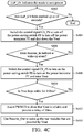
- Figs. 4A , 4B and 4C show waveforms and a flowchart for the power-saving switch control circuit 204, with reference to the power status of the chipset mounted on the motherboard.
- Figs. 4A , 4B and 4C are discussed with respect to figs. 2 and 3 .
- a chipset signal SLP_S5# transits from high to low and a power-saving enable signal EuP_EN changes.
- the power-saving enable signal EuP_EN is coupled to the chipset signal SLP_S5#.
- the chipset signal SLP_S5# is high, the system is operated in the normal power state S0 and the power-saving enable signal EuP_EN is not triggered.
- the chipset signal SLP_S5# is low, the system is operated in the standby power state S5 and the power-saving enable signal EuP_EN is switched to the enable state.
- the control signal CS_PS of the power switch PS is switched to turn off the power-saving switch PS.
- the power transistor PT is turned off and the second voltage Vout drops.
- the power consumption reduces and the system is switched to a power-saving mode.
- the system in the power-saving mode complies EuP/ErP (Energy Using Product/Energy Related Product) regulations. It means that in the power-saving mode the entire system (including the power supply) consumes less than 0.5W, and less than 0.25W is consumed by the system except for the power supply of the system. In an exemplary embodiment, the system consumes less power in the power-saving mode than in the standby mode S5.
- the system and the chipset mounted on the motherboard of the system is switched from the power-saving mode to the standby power state S5.
- the resumption trigger signal Resume_In is triggered in accordance with the wake-up event.
- the control signal CS_PS is switched to turn on the power-saving switch PS and, accordingly, the power transistor PT is turned on and the second voltage Vout rises.
- the power flag PWRGD is asserted to show that the second voltage Vout is reliable and, after 20ms (depending on system settings), the resumption output signal Resume_Out outputs a wake-up event to the chipset then the chipset de-asserts its signal SLP S5#.
- the chipset and whole system switch from the standby power state S5 to the normal power state S0.
- Fig. 4C is a flowchart depicting the operations of the power-saving switch control circuit 204.
- step S402 is performed to determine whether the power-saving enable signal EuP_EN has been kept enabled for a predetermined time period, e.g. 10 seconds. When less than 10 seconds, the procedure ends.
- the control signal CS_PS is switched to turn off the power-saving switch PS to turn off the power transistor PT and thereby the second voltage Vout is shut down (step S404).
- the resumption trigger signal Resume_In is monitored for detection of any wake-up event.
- Step S406 is repeated when no wake-up event occurs.
- the control signal CS_PS is switched to turn on the power-saving switch PS to turn on the power transistor PT and thereby the second voltage Vout rises (step S408).
- the second voltage Vout is monitored to determine whether the second voltage Vout has been stable for a predetermined time period, e.g. 150ms. If no, step S410 is repeated.
- step S412 is performed to assert the power flag PWRGD to show that the second voltage Vout is reliable and to provide a delay of a predetermined time period, e.g. 20ms. After the delayed 20ms, step S414 is performed to use the resumption output signal Resume_Out to wake up the rear modules powered by the second voltage Vout.
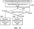
- Figs. 5A, 5B and 5C show waveforms and a flowchart for the voltage evaluation logic circuit 206. Figs. 5A, 5B and 5C are discussed with respect to figs. 2 and 3 .
- the second voltage Vout is raised when the first voltage Vin is powered on.
- the second voltage Vout rises higher than a lower limit Vout_LT for 150ms (depending on the system settings), the power flag PWRGD is asserted to show that the second voltage Vout is reliable.
- the power flag PWRGD is de-asserted without waiting for the transition of the second voltage Vout to show that the second voltage Vout is unreliable.
- the power flag PWRGD is de-asserted instantly to show that the second voltage Vout is unreliable.
- Fig. 5C is a flowchart depicting the operations of the voltage evaluation circuit 206.
- step S502 is performed to assert the power flag PWRGD to show that the second voltage Vout is good.
- step S504 the first voltage Vin and the second voltage Vout are monitored.
- step S506 is performed to de-assert the power flag PWRGD to show that the second voltage Vout is bad.
- step S508 is performed to de-assert the power flag PWRGD to show that the second voltage Vout is bad.
- the voltage regulator of the disclosure may be manufactured into chips.
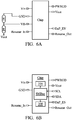
- Figs. 6A to 6D show the variants of the voltage regulator 300, not completely packaged in one chip.
- a voltage divider generating the feedback voltage Vfb is external to the chip.
- the chip has a pin for reception of the feedback voltage Vfb.
- the voltage divider, external to the chip, for generation of the feedback voltage Vfb therefore, is easily modified (e.g. just changing the resistance of the voltage divider resistors) for Vout adjustment according to the user's needs.
- two resistors both labeled R
- the voltage divider of fig. 6A for generation of the feedback voltage Vfb may be replaced by other feedback designs.
- SMBus System Management Bus
- the chip provides pins for reception of timer control signals SCL and SDA.
- the timer control signals SCL and SDA received from outside of the chip are transmitted through the SMBus to set the timing threshold of the timer 316 of the voltage evaluation logic circuit 206 and the timing threshold of the timer 308 of the power-saving control circuit 204.
- a circuit generating a voltage VC1 as a lower limit Vin_LT for the first voltage Vin is external to the chip.
- the chip has a pin for reception of the voltage VC1.
- the voltage divider for generation of the voltage VC1 is easily modified (e.g. just changing the resistance of the voltage divider resistors).
- two resistors both labeled R are provided to form a voltage divider to generate the voltage VC1 as the lower limit Vin_LT.
- the lower limit Vin_LT may be determined in other ways.
- the voltage VC1 is generated by the voltage divider dividing the first voltage Vin and may be provided within the chip.
- a circuit generating a voltage VC2 as a lower limit Vout_LT for the second voltage Vout is external to the chip.
- the chip has a pin for reception of the voltage VC2.
- the voltage divider for generation of the voltage VC2 is easily modified (e.g. just changing the resistance of the voltage divider resistors).
- two resistors both labeled R
- the lower limit Vout_LT may be determined in other ways.
- the voltage VC2 is generated by the voltage divider dividing the second voltage Vout and may be provided within the chip.
- Fig. 7 depicts a voltage regulator 700 in accordance with an exemplary embodiment of the disclosure, wherein a fundamental structure (corresponding to block 202 of fig. 2 ) for voltage regulation based on the switching voltage regulator design is depicted As shown, the power-saving switch PS is provided between a pulse control circuit 702 and a driver 704 of the power transistor PT.
- a fundamental structure corresponding to block 202 of fig. 2
- the power-saving switch PS is provided between a pulse control circuit 702 and a driver 704 of the power transistor PT.
Landscapes
- Engineering & Computer Science (AREA)
- Power Engineering (AREA)
- Business, Economics & Management (AREA)
- Emergency Management (AREA)
- Continuous-Control Power Sources That Use Transistors (AREA)
- Charge And Discharge Circuits For Batteries Or The Like (AREA)
Claims (15)
- Transformatorloser Spannungsregler (200), umfassend:Einen Leistungstransistor (PT), der eine Umwandlung von einer ersten Spannung in eine zweite Spannung antreibt und einen Steueranschluss aufweist;Einen Energiesparschalter (PS) mit einem Anschluss, der mit dem Steueranschluss des Leistungstransistors gekoppelt ist; undEine Energiesparschalter-Steuerschaltung (204), die den Energiesparschalter steuert,wobei:Wenn der Energiesparschalter eingeschaltet wird, ist ein Steuersignal (CS_PT) für den Leistungstransistor an den Steueranschluss des Leistungstransistors gekoppelt ist; undWenn der Energiesparschalter ausgeschaltet wird, ist das Steuersignal für den Leistungstransistor von dem Steueranschluss des Leistungstransistors entkoppelt;Die Energiesparschalter-Steuerschaltung schaltet den Energiesparschalter ab, wenn ein von der zweiten Spannung gespeistes Modul in den Standby-Modus geschaltet wird.
- Der Spannungsregler nach Anspruch 1, ferner umfassend:
Eine Spannungsauswerteschaltung, die ein Leistungsmerkmal ausgibt, um anzuzeigen, ob die zweite Spannung entsprechend der ersten Spannung und der zweiten Spannung zuverlässig ist. - Der Spannungsregler nach einem der Ansprüche 1 bis 2, wobei:Die Energiesparschalter-Steuerschaltung ferner einen Timer umfasst, um zu bestimmen, ob ein Energiespar- Freigabesignal für eine vorbestimmte Zeitdauer aktiviert bleibt, und wenn das Energiespar- Freigabesignal für die vorbestimmte Zeitdauer aktiviert bleibt, erzeugt die Energiesparschalter-Steuerschaltung ein Steuersignal für den Energiesparschalter, um den Energiesparschalter abzuschalten; undWird das Energiespar- Freigabesignal in einen Freigabezustand geschaltet, wenn das von der zweiten Spannung gespeiste Modul in den Standby-Modus geschaltet wird.
- Der Spannungsregler nach einem der Ansprüche 1 bis 3, wobei:
Die Energiesparschalter-Steuerschaltung ferner einen internen Pull-Down-Widerstand aufweist, der mit einem Empfangsanschluss gekoppelt ist, der von der Energiesparschalter-Steuerschaltung zum Empfang des Energiespar- Freigabesignals bereitgestellt wird. - Der Spannungsregler nach einem der Ansprüche 1 bis 4 wobei:
Die Energiesparschalter-Steuerschaltung erhält weiterhin ein Wiederaufnahme-Trigger-Signal, und wenn das Wiederaufnahme-Trigger-Signal ein Weckereignis anzeigt, steuert die Energiesparschalter-Steuerschaltung den Energiesparschalter, um den Energiesparschalter einzuschalten. - Der Spannungsregler nach einem der Ansprüche 1 bis 5, wobei:
Die Energiesparschalter-Steuerschaltung außerdem ein Wiederaufnahme-Ausgangssignal erzeugt, das das von der zweiten Spannung gespeiste Modul aufweckt, wenn das Power-Flag anzeigt, dass die zweite Spannung zuverlässig ist. - Der Spannungsregler nach einem der Ansprüche 1 bis 6, wobei die Spannungsauswertungslogikschaltung umfasst:Einen ersten Komparator, der vergleicht, ob die erste Spannung kleiner als eine untere Grenze der ersten Spannung ist;Einen zweiten Komparator, der vergleicht, ob die zweite Spannung höher als eine untere Grenze der zweiten Spannung ist; undEinen Timer, der an einen Ausgangsanschluss des zweiten Komparators gekoppelt ist, um zu prüfen, ob die zweite Spannung für eine vorbestimmte Zeitspanne über die untere Grenze der zweiten Spannung gestiegen ist.
- Der Spannungsregler nach einem der Ansprüche 1 bis 7, wobei:Die Spannungsauswertungslogikschaltung das Leistungsmerkmal deaktiviert, um anzuzeigen, dass die zweite Spannung unzuverlässig ist, wenn der erste Komparator anzeigt, dass die erste Spannung niedriger als die untere Grenze der ersten Spannung ist; unddie Spannungsauswertungslogikschaltung das Leistungsmerkmal bestätigt, um anzuzeigen, dass die zweite Spannung zuverlässig ist, wenn der zweite Komparator zeigt, dass die zweite Spannung während der vorgegebenen Zeitspanne über die untere Grenze der zweiten Spannung ansteigt; oderDie Spannungsauswertungslogikschaltung deaktiviert weiterhin das Leistungsmerkmal, um anzuzeigen, dass die zweite Spannung unzuverlässig ist, wenn der zweite Komparator zeigt, dass die zweite Spannung unter die untere Grenze der zweiten Spannung fällt.
- Der Spannungsregler nach einem der Ansprüche 1 bis 8, weiterhin umfassend:Einen Chip, bestehend aus dem Leistungstransistor, dem Energiesparschalter, der Energiesparschalter-Steuerschaltung sowie einem Systemmanagement-Bus;wobei:Der Chip einen ersten Pin, der mit der ersten Spannung verbunden ist, einen zweiten Pin, der die zweite Spannung ausgibt, einen dritten Pin, der mit Masse verbunden ist, einen vierten Pin, der das Energiespar- Freigabesignal empfängt, und einen fünften bzw. sechsten Pin zum Empfangen von Timersteuersignalen enthält; undDer Chip die vorgegebene Zeitdauer entsprechend dem Timer der Energiesparschaltung über den Systemmanagementbus auf Basis des Timersteuersignals des fünften und sechsten Pins einstellt.
- Der Spannungsregler nach einem der Ansprüche 1 bis 9, umfassend:Einen Chip, bestehend aus dem Leistungstransistor, dem Energiesparschalter, der Energiesparschalter-Steuerschaltung , der Spannungsauswertungslogik sowie einem Systemmanagementbus,Wobei der Chip einen ersten Pin, der mit der ersten Spannung gekoppelt ist, einen zweiten Pin, der die zweite Spannung ausgibt, einen dritten Pin, der mit Masse gekoppelt ist, einen vierten Pin, der das Power-Flag ausgibt, und einen fünften und einen sechsten Pin zum Empfangen von Timersteuersignalen aufweist; undder Chip die vorbestimmte Zeitdauer entsprechend dem Timer der Spannungsauswertungslogikschaltung über den Systemmanagementbus auf der Grundlage des Timersteuersignals, das vom fünften und sechsten Pin empfangen wird, einstellt.
- Der Spannungsregler nach einem der Ansprüche 1 bis 10, umfassend:Einen Chip, der den Leistungstransistor, den Energiesparschalter, die Energiesparschalter-Steuerschaltung und die Spannungsauswertungslogikschaltung umfasst, wobei der Chip eine Vielzahl von Pins aufweist, die mit der ersten Spannung gekoppelt sind, die zweite Spannung ausgeben, mit der Masse koppelt sind, das Leistungsmerkmal ausgeben und die untere Grenze der ersten Spannung empfangen, und die untere Grenze der ersten Spannung dem ersten Komparator der Spannungsauswertungslogikschaltung innerhalb des Chips bereitgestellt wird, um zu überprüfen, ob die erste Spannung niedriger als die untere Grenze der ersten Spannung ist; undEine Einstellschaltung außerhalb des Chips, wobei die Einstellschaltung die untere Grenze der ersten Spannung setzt und die untere Grenze der ersten Spannung in den Chip eingibt;oder bestehend ausEinem Chip, der den Leisiungstransistor, den Energiesparschalter, die Energiesparschalter-Steuerschaltung und die Spannungsauswertungslogikschaltung umfasst, wobei der Chip eine Vielzahl von Pins aufweist, die mit der ersten Spannung koppeln, die zweite Spannung ausgeben, an Masse koppeln, das Leistungsmerkmal ausgeben und die untere Grenze der zweiten Spannung empfangen, und die untere Grenze der zweiten Spannung dem zweiten Komparator der Spannungsauswertungslogikschaltung innerhalb des Chips bereitgestellt wird, um die zweite Spannung mit der unteren Grenze der zweiten Spannung zu vergleichen; undEine Einstellschaltung, die außerhalb des Chips und mit einem der Pins gekoppelt ist, der die zweite Spannung ausgibt, wobei die Einstellschaltung die untere Grenze der zweiten Spannung einstellt und die untere Grenze der zweiten Spannung in den Chip eingibt.
- Verfahren zur Spannungsregelung, umfassend:Bereitstellen eines Energiesparschalters (PS) in einem transformatorlosen Spannungsregler, wobei der Energiesparschalter einen Anschluss aufweist, der mit einem Steueranschluss (PTcon) eines Leistungstransistors (PT) des Spannungsreglers gekoppelt ist und der Leistungstransistor eine Umwandlung von einer ersten Spannung (Vin) in eine zweite Spannung (Vout) steuert, wobei ein Steuersignal (CS PT) für den Leistungstransistor mit dem Steueranschluss des Leistungstransistors gekoppelt ist, wenn der Energiesparschalter eingeschaltet ist, und das Steuersignal für den Leistungstransistor von dem Steueranschluss des Leistungstransistors getrennt ist, wenn der Energiesparschalter ausgeschaltet ist; undAusschalten des Energiesparschalters, wenn ein von der zweiten Spannung gespeistes Modul in den Standby-Modus geschaltet wird.
- Ein Spannungsreglerchip, bestehend aus:Einen Leistungstransistor (PT), der eine Umwandlung von einer ersten Spannung (Vin) in eine zweite Spannung (Vout) steuert und einen Steueranschluss (PTcon) aufweist;Einen Energiesparschalter (PS) mit einem Anschluss, der mit dem Steueranschluss des Leistungstransistors gekoppelt ist, um ein Steuersignal (CS PT) für den Leistungstransistor mit dem Steueranschluss des Leistungstransistors zu koppeln, wenn der Energiesparschalter eingeschaltet ist, und das Steuersignal für den Leistungstransistor von dem Steueranschluss des Leistungstransistors zu entkoppeln, wenn der Energiesparschalter ausgeschaltet ist, wobei der Energiesparschalter ausgeschaltet wird, wenn ein von der zweiten Spannung versorgtes Modul in einen Standby-Modus geschaltet wird;Eine Energiesparschalter-Steuerschaltung (204), die den Energiesparschalter steuert;Einen ersten Pin, der mit der ersten Spannung gekoppelt ist;Einen zweiten Pin, der die zweite Spannung ausgibt;Einen dritten Pin, der mit Masse verbunden ist; undEinen vierten Pin, der eine Feedback- Spannung empfängt,Wobei der Chip die Feedback- Spannung (Vfb) erhält, um das Steuersignal für den Leistungstransistor einzustellen.
- Der Spannungsreglerchip nach Anspruch 13, weiterhin umfassend:Einen fünften Pin, der ein Power-Flag ausgibt, um anzuzeigen, ob die zweite Spannung zuverlässig ist,wobei:Das Power-Flag deaktiviert ist, um anzuzeigen, dass die zweite Spannung unzuverlässig ist, wenn die erste Spannung unter eine untere Grenze der ersten Spannung fällt;Das Power-Flag deaktiviert ist, um anzuzeigen, dass die zweite Spannung unzuverlässig ist, wenn die zweite Spannung unter eine untere Grenze der zweiten Spannung fällt; undDas Power-Flag aktiviert ist, um zu zeigen, dass die zweite Spannung zuverlässig ist, wenn die zweite Spannung für einen vorbestimmten Zeitraum über die untere Grenze der zweiten Spannung gestiegen ist.
- Der Spannungsreglerchip nach Anspruch 13 oder 14, ferner umfassend:Einen sechsten Pin, der ein Energiespar- Freigabesignal empfängt, um ein Steuersignal für den Energiesparschalter zum Ein- oder Ausschalten des Energiesparschalters zu schalten, wobei das Energiespar- Freigabesignal in einen Freigabezustand schaltet, um den Energiesparschalter auszuschalten, wenn das von der zweiten Spannung gespeiste Modul in den Standby-Modus geschaltet wird;Einen siebten Pin, der ein Wiederaufnahme-Triggersignal empfängt, wobei, wenn das Wiederaufnahme-Triggersignal ein Weckereignis anzeigt, das Steuersignal für den Energiesparschalter geschaltet wird, um den Energiesparschalter einzuschalten; undEin achter Pin, der ein Wiederaufnahme-Ausgangssignal ausgibt, das so geschaltet wird, dass es das von der zweiten Spannung gespeiste Modul aufweckt, wenn ein Power-Flag anzeigt, dass die zweite Spannung zuverlässig ist.
Applications Claiming Priority (1)
| Application Number | Priority Date | Filing Date | Title |
|---|---|---|---|
| TW103116198A TWI503645B (zh) | 2014-05-07 | 2014-05-07 | 電壓調節器、方法與晶片 |
Publications (2)
| Publication Number | Publication Date |
|---|---|
| EP2947536A1 EP2947536A1 (de) | 2015-11-25 |
| EP2947536B1 true EP2947536B1 (de) | 2018-07-25 |
Family
ID=51492217
Family Applications (1)
| Application Number | Title | Priority Date | Filing Date |
|---|---|---|---|
| EP14183894.6A Active EP2947536B1 (de) | 2014-05-07 | 2014-09-08 | Spannungsregler und Verfahren zur Regelung der Spannung und Chip damit |
Country Status (4)
| Country | Link |
|---|---|
| US (1) | US9515552B2 (de) |
| EP (1) | EP2947536B1 (de) |
| CN (1) | CN105094195B (de) |
| TW (1) | TWI503645B (de) |
Families Citing this family (10)
| Publication number | Priority date | Publication date | Assignee | Title |
|---|---|---|---|---|
| US9851730B2 (en) | 2015-04-10 | 2017-12-26 | Qualcomm Incorporated | Voltage droop control |
| US9876428B2 (en) * | 2015-05-13 | 2018-01-23 | Skyworks Solutions, Inc. | Circuits, devices and methods related to internal supply for voltage regulators |
| CN112564479A (zh) * | 2016-11-18 | 2021-03-26 | 华为技术有限公司 | 调压电路及调压方法 |
| CN108121426B (zh) * | 2016-11-30 | 2020-08-11 | 龙芯中科技术有限公司 | 芯片电压调节方法、装置及系统 |
| JP6795388B2 (ja) * | 2016-12-15 | 2020-12-02 | エイブリック株式会社 | 電圧異常検出回路及び半導体装置 |
| KR102344760B1 (ko) | 2017-02-14 | 2021-12-31 | 한국전자통신연구원 | 논리회로의 제어에 따라 적은 전력을 소비하는 전자회로, 선형 레귤레이팅 회로, 및 dc-dc 컨버팅 회로 |
| JP6814085B2 (ja) * | 2017-03-31 | 2021-01-13 | エイブリック株式会社 | 監視回路及び半導体装置 |
| US10424385B1 (en) * | 2018-08-28 | 2019-09-24 | Dell Products L. P. | Self-configuring integrated circuit device |
| CN113031738B (zh) * | 2021-03-12 | 2024-05-07 | 维沃移动通信有限公司 | 一种芯片供电电路及方法 |
| CN114142939B (zh) * | 2021-12-03 | 2023-08-08 | 青岛海信宽带多媒体技术有限公司 | 一种光模块和光模块los优化方法 |
Family Cites Families (21)
| Publication number | Priority date | Publication date | Assignee | Title |
|---|---|---|---|---|
| GB9623612D0 (en) | 1996-11-13 | 1997-01-08 | Rca Thomson Licensing Corp | Separate power supplies for standby operation |
| KR100229604B1 (ko) * | 1996-11-14 | 1999-11-15 | 윤종용 | 역률보정회로를 갖는 디스플레이 모니터 전원 공급 장치 |
| KR100603926B1 (ko) | 1999-10-25 | 2006-07-24 | 삼성전자주식회사 | 여러 전원 관리 상태를 갖는 컴퓨터 시스템을 위한 전원 공급 제어 회로 및 그의 제어 방법 |
| US6603292B1 (en) | 2001-04-11 | 2003-08-05 | National Semiconductor Corporation | LDO regulator having an adaptive zero frequency circuit |
| US20030011247A1 (en) | 2001-07-16 | 2003-01-16 | Matsushita Electric Industrial Co., Ltd. | Power supply device |
| AT413617B (de) | 2002-05-14 | 2006-04-15 | Siemens Ag Oesterreich | Ladenetzteil |
| US6979987B2 (en) * | 2002-11-14 | 2005-12-27 | Fyre Storm, Inc. | Method of regulating an output voltage of a power converter by sensing the output voltage during a first time interval and calculating a next current value in an inductor sufficient to bring the output voltage to a target voltage within a second time interval immediately following the first time interval and varying a duty cycle of a switch during the second time interval |
| KR100608112B1 (ko) | 2004-08-27 | 2006-08-02 | 삼성전자주식회사 | 과전류 보호회로를 구비한 전원 레귤레이터 및 전원레귤레이터의 과전류 보호방법 |
| US7208925B2 (en) | 2004-09-01 | 2007-04-24 | Intel Corporation | Voltage regulator controller power good indicator circuitry |
| US7439718B2 (en) | 2004-09-30 | 2008-10-21 | Freescale Semiconductor, Inc. | Apparatus and method for high speed voltage regulation |
| CN1322649C (zh) * | 2004-11-15 | 2007-06-20 | 刘利军 | 家用节电器 |
| US7106032B2 (en) * | 2005-02-03 | 2006-09-12 | Aimtron Technology Corp. | Linear voltage regulator with selectable light and heavy load paths |
| US7454637B2 (en) * | 2005-09-02 | 2008-11-18 | Intel Corporation | Voltage regulator having reduced droop |
| US7459891B2 (en) | 2006-03-15 | 2008-12-02 | Texas Instruments Incorporated | Soft-start circuit and method for low-dropout voltage regulators |
| JP4869839B2 (ja) * | 2006-08-31 | 2012-02-08 | 株式会社リコー | ボルテージレギュレータ |
| TW200928650A (en) * | 2007-12-26 | 2009-07-01 | Hon Hai Prec Ind Co Ltd | Voltage regulating circuit of motherboard |
| KR101443583B1 (ko) * | 2008-04-29 | 2014-11-03 | 세미컨덕터 콤포넨츠 인더스트리즈 엘엘씨 | 출력 전압을 조절하는 방법 |
| US8599589B2 (en) * | 2008-10-13 | 2013-12-03 | Apple Inc. | Methods and systems for reducing power consumption |
| US20130169246A1 (en) * | 2011-12-28 | 2013-07-04 | Skymedi Corporation | Linear voltage regulating circuit adaptable to a logic system |
| US20130176009A1 (en) * | 2012-01-10 | 2013-07-11 | Monolithic Power Systems, Inc. | Smart low drop-out voltage regulator and associated method |
| CN203039571U (zh) * | 2012-11-09 | 2013-07-03 | 福建捷联电子有限公司 | PFC的Vcc供电电压开启电路及应用其的开关电源 |
-
2014
- 2014-05-07 TW TW103116198A patent/TWI503645B/zh active
- 2014-06-27 CN CN201410298561.4A patent/CN105094195B/zh active Active
- 2014-08-04 US US14/450,638 patent/US9515552B2/en active Active
- 2014-09-08 EP EP14183894.6A patent/EP2947536B1/de active Active
Non-Patent Citations (1)
| Title |
|---|
| None * |
Also Published As
| Publication number | Publication date |
|---|---|
| TW201543192A (zh) | 2015-11-16 |
| US20150326119A1 (en) | 2015-11-12 |
| TWI503645B (zh) | 2015-10-11 |
| CN105094195B (zh) | 2017-02-15 |
| CN105094195A (zh) | 2015-11-25 |
| US9515552B2 (en) | 2016-12-06 |
| EP2947536A1 (de) | 2015-11-25 |
Similar Documents
| Publication | Publication Date | Title |
|---|---|---|
| US9515552B2 (en) | Voltage regulator and voltage regulating method and chip using the same | |
| US8698792B2 (en) | Low-power display control method and associated display controller | |
| US9430008B2 (en) | Apparatus and method for optimizing use of NVDC chargers | |
| US9667095B2 (en) | Electronic apparatus | |
| US6707281B2 (en) | Method and apparatus for operating a voltage regulator based on inductor current detection | |
| US20100073351A1 (en) | Ultra-Low-Power Display Control Circuit and Associated Method | |
| US9195297B2 (en) | Bridging device for connecting to a host executes a power saving operation or a polling operation according to status detected by the connection detector | |
| JP4889398B2 (ja) | 定電圧電源回路 | |
| US10019022B2 (en) | Level shifting module and power circuit and method of operating level shifting module | |
| US20100250983A1 (en) | Power saving control system | |
| KR20170046851A (ko) | 표시장치, 구동집적회로, 터치구동회로 및 구동전원회로 | |
| US8013644B2 (en) | Power supply circuit for south bridge chip | |
| US20080012585A1 (en) | Apparatus and method of adjusting system efficiency | |
| CN101556499B (zh) | 电流调整装置、供电装置、以及电流调整方法 | |
| US8181053B2 (en) | Power saving device and all-in-one PC having the same for controlling standby power to memory controller and memory | |
| US20100066342A1 (en) | Control circuit for single chip ic | |
| US10216253B2 (en) | Universal serial bus hub and control method thereof | |
| US7594130B1 (en) | Circuit for regulating timing sequence | |
| US20130151881A1 (en) | Bridging device and power saving method thereof | |
| US9996143B2 (en) | Apparatus and method for selectively disabling one or more analog circuits of a processor during a low power state of the processor | |
| US20170315571A1 (en) | Semiconductor device and power source supply method | |
| CN105589501B (zh) | 节能的控制芯片及其控制系统 | |
| TWI587116B (zh) | 電壓調節晶片 | |
| US7831848B2 (en) | Power management system for use in laptop computer and management method thereof | |
| US9753515B2 (en) | Anti-deadlock circuit for voltage regulator and associated power system |
Legal Events
| Date | Code | Title | Description |
|---|---|---|---|
| PUAI | Public reference made under article 153(3) epc to a published international application that has entered the european phase |
Free format text: ORIGINAL CODE: 0009012 |
|
| AK | Designated contracting states |
Kind code of ref document: A1 Designated state(s): AL AT BE BG CH CY CZ DE DK EE ES FI FR GB GR HR HU IE IS IT LI LT LU LV MC MK MT NL NO PL PT RO RS SE SI SK SM TR |
|
| AX | Request for extension of the european patent |
Extension state: BA ME |
|
| 17P | Request for examination filed |
Effective date: 20160520 |
|
| RBV | Designated contracting states (corrected) |
Designated state(s): AL AT BE BG CH CY CZ DE DK EE ES FI FR GB GR HR HU IE IS IT LI LT LU LV MC MK MT NL NO PL PT RO RS SE SI SK SM TR |
|
| GRAP | Despatch of communication of intention to grant a patent |
Free format text: ORIGINAL CODE: EPIDOSNIGR1 |
|
| STAA | Information on the status of an ep patent application or granted ep patent |
Free format text: STATUS: GRANT OF PATENT IS INTENDED |
|
| RIC1 | Information provided on ipc code assigned before grant |
Ipc: H02J 9/00 20060101ALI20180301BHEP Ipc: G05F 1/56 20060101AFI20180301BHEP |
|
| INTG | Intention to grant announced |
Effective date: 20180321 |
|
| GRAS | Grant fee paid |
Free format text: ORIGINAL CODE: EPIDOSNIGR3 |
|
| GRAA | (expected) grant |
Free format text: ORIGINAL CODE: 0009210 |
|
| STAA | Information on the status of an ep patent application or granted ep patent |
Free format text: STATUS: THE PATENT HAS BEEN GRANTED |
|
| AK | Designated contracting states |
Kind code of ref document: B1 Designated state(s): AL AT BE BG CH CY CZ DE DK EE ES FI FR GB GR HR HU IE IS IT LI LT LU LV MC MK MT NL NO PL PT RO RS SE SI SK SM TR |
|
| REG | Reference to a national code |
Ref country code: GB Ref legal event code: FG4D |
|
| REG | Reference to a national code |
Ref country code: CH Ref legal event code: EP |
|
| REG | Reference to a national code |
Ref country code: AT Ref legal event code: REF Ref document number: 1022425 Country of ref document: AT Kind code of ref document: T Effective date: 20180815 |
|
| REG | Reference to a national code |
Ref country code: IE Ref legal event code: FG4D |
|
| REG | Reference to a national code |
Ref country code: DE Ref legal event code: R096 Ref document number: 602014029007 Country of ref document: DE |
|
| REG | Reference to a national code |
Ref country code: FR Ref legal event code: PLFP Year of fee payment: 5 |
|
| REG | Reference to a national code |
Ref country code: NL Ref legal event code: FP |
|
| REG | Reference to a national code |
Ref country code: LT Ref legal event code: MG4D |
|
| PG25 | Lapsed in a contracting state [announced via postgrant information from national office to epo] |
Ref country code: SE Free format text: LAPSE BECAUSE OF FAILURE TO SUBMIT A TRANSLATION OF THE DESCRIPTION OR TO PAY THE FEE WITHIN THE PRESCRIBED TIME-LIMIT Effective date: 20180725 Ref country code: PL Free format text: LAPSE BECAUSE OF FAILURE TO SUBMIT A TRANSLATION OF THE DESCRIPTION OR TO PAY THE FEE WITHIN THE PRESCRIBED TIME-LIMIT Effective date: 20180725 Ref country code: RS Free format text: LAPSE BECAUSE OF FAILURE TO SUBMIT A TRANSLATION OF THE DESCRIPTION OR TO PAY THE FEE WITHIN THE PRESCRIBED TIME-LIMIT Effective date: 20180725 Ref country code: GR Free format text: LAPSE BECAUSE OF FAILURE TO SUBMIT A TRANSLATION OF THE DESCRIPTION OR TO PAY THE FEE WITHIN THE PRESCRIBED TIME-LIMIT Effective date: 20181026 Ref country code: NO Free format text: LAPSE BECAUSE OF FAILURE TO SUBMIT A TRANSLATION OF THE DESCRIPTION OR TO PAY THE FEE WITHIN THE PRESCRIBED TIME-LIMIT Effective date: 20181025 Ref country code: BG Free format text: LAPSE BECAUSE OF FAILURE TO SUBMIT A TRANSLATION OF THE DESCRIPTION OR TO PAY THE FEE WITHIN THE PRESCRIBED TIME-LIMIT Effective date: 20181025 Ref country code: IS Free format text: LAPSE BECAUSE OF FAILURE TO SUBMIT A TRANSLATION OF THE DESCRIPTION OR TO PAY THE FEE WITHIN THE PRESCRIBED TIME-LIMIT Effective date: 20181125 Ref country code: LT Free format text: LAPSE BECAUSE OF FAILURE TO SUBMIT A TRANSLATION OF THE DESCRIPTION OR TO PAY THE FEE WITHIN THE PRESCRIBED TIME-LIMIT Effective date: 20180725 Ref country code: FI Free format text: LAPSE BECAUSE OF FAILURE TO SUBMIT A TRANSLATION OF THE DESCRIPTION OR TO PAY THE FEE WITHIN THE PRESCRIBED TIME-LIMIT Effective date: 20180725 |
|
| PG25 | Lapsed in a contracting state [announced via postgrant information from national office to epo] |
Ref country code: HR Free format text: LAPSE BECAUSE OF FAILURE TO SUBMIT A TRANSLATION OF THE DESCRIPTION OR TO PAY THE FEE WITHIN THE PRESCRIBED TIME-LIMIT Effective date: 20180725 Ref country code: AL Free format text: LAPSE BECAUSE OF FAILURE TO SUBMIT A TRANSLATION OF THE DESCRIPTION OR TO PAY THE FEE WITHIN THE PRESCRIBED TIME-LIMIT Effective date: 20180725 Ref country code: LV Free format text: LAPSE BECAUSE OF FAILURE TO SUBMIT A TRANSLATION OF THE DESCRIPTION OR TO PAY THE FEE WITHIN THE PRESCRIBED TIME-LIMIT Effective date: 20180725 |
|
| REG | Reference to a national code |
Ref country code: DE Ref legal event code: R097 Ref document number: 602014029007 Country of ref document: DE |
|
| PG25 | Lapsed in a contracting state [announced via postgrant information from national office to epo] |
Ref country code: CZ Free format text: LAPSE BECAUSE OF FAILURE TO SUBMIT A TRANSLATION OF THE DESCRIPTION OR TO PAY THE FEE WITHIN THE PRESCRIBED TIME-LIMIT Effective date: 20180725 Ref country code: IT Free format text: LAPSE BECAUSE OF FAILURE TO SUBMIT A TRANSLATION OF THE DESCRIPTION OR TO PAY THE FEE WITHIN THE PRESCRIBED TIME-LIMIT Effective date: 20180725 Ref country code: RO Free format text: LAPSE BECAUSE OF FAILURE TO SUBMIT A TRANSLATION OF THE DESCRIPTION OR TO PAY THE FEE WITHIN THE PRESCRIBED TIME-LIMIT Effective date: 20180725 Ref country code: EE Free format text: LAPSE BECAUSE OF FAILURE TO SUBMIT A TRANSLATION OF THE DESCRIPTION OR TO PAY THE FEE WITHIN THE PRESCRIBED TIME-LIMIT Effective date: 20180725 Ref country code: MC Free format text: LAPSE BECAUSE OF FAILURE TO SUBMIT A TRANSLATION OF THE DESCRIPTION OR TO PAY THE FEE WITHIN THE PRESCRIBED TIME-LIMIT Effective date: 20180725 Ref country code: ES Free format text: LAPSE BECAUSE OF FAILURE TO SUBMIT A TRANSLATION OF THE DESCRIPTION OR TO PAY THE FEE WITHIN THE PRESCRIBED TIME-LIMIT Effective date: 20180725 |
|
| REG | Reference to a national code |
Ref country code: CH Ref legal event code: PL |
|
| PG25 | Lapsed in a contracting state [announced via postgrant information from national office to epo] |
Ref country code: SK Free format text: LAPSE BECAUSE OF FAILURE TO SUBMIT A TRANSLATION OF THE DESCRIPTION OR TO PAY THE FEE WITHIN THE PRESCRIBED TIME-LIMIT Effective date: 20180725 Ref country code: SM Free format text: LAPSE BECAUSE OF FAILURE TO SUBMIT A TRANSLATION OF THE DESCRIPTION OR TO PAY THE FEE WITHIN THE PRESCRIBED TIME-LIMIT Effective date: 20180725 Ref country code: DK Free format text: LAPSE BECAUSE OF FAILURE TO SUBMIT A TRANSLATION OF THE DESCRIPTION OR TO PAY THE FEE WITHIN THE PRESCRIBED TIME-LIMIT Effective date: 20180725 |
|
| PLBE | No opposition filed within time limit |
Free format text: ORIGINAL CODE: 0009261 |
|
| STAA | Information on the status of an ep patent application or granted ep patent |
Free format text: STATUS: NO OPPOSITION FILED WITHIN TIME LIMIT |
|
| REG | Reference to a national code |
Ref country code: BE Ref legal event code: MM Effective date: 20180930 |
|
| REG | Reference to a national code |
Ref country code: IE Ref legal event code: MM4A |
|
| PG25 | Lapsed in a contracting state [announced via postgrant information from national office to epo] |
Ref country code: LU Free format text: LAPSE BECAUSE OF NON-PAYMENT OF DUE FEES Effective date: 20180908 |
|
| 26N | No opposition filed |
Effective date: 20190426 |
|
| PG25 | Lapsed in a contracting state [announced via postgrant information from national office to epo] |
Ref country code: IE Free format text: LAPSE BECAUSE OF NON-PAYMENT OF DUE FEES Effective date: 20180908 |
|
| PG25 | Lapsed in a contracting state [announced via postgrant information from national office to epo] |
Ref country code: SI Free format text: LAPSE BECAUSE OF FAILURE TO SUBMIT A TRANSLATION OF THE DESCRIPTION OR TO PAY THE FEE WITHIN THE PRESCRIBED TIME-LIMIT Effective date: 20180725 Ref country code: BE Free format text: LAPSE BECAUSE OF NON-PAYMENT OF DUE FEES Effective date: 20180930 Ref country code: LI Free format text: LAPSE BECAUSE OF NON-PAYMENT OF DUE FEES Effective date: 20180930 Ref country code: CH Free format text: LAPSE BECAUSE OF NON-PAYMENT OF DUE FEES Effective date: 20180930 |
|
| PG25 | Lapsed in a contracting state [announced via postgrant information from national office to epo] |
Ref country code: MT Free format text: LAPSE BECAUSE OF NON-PAYMENT OF DUE FEES Effective date: 20180908 |
|
| PG25 | Lapsed in a contracting state [announced via postgrant information from national office to epo] |
Ref country code: TR Free format text: LAPSE BECAUSE OF FAILURE TO SUBMIT A TRANSLATION OF THE DESCRIPTION OR TO PAY THE FEE WITHIN THE PRESCRIBED TIME-LIMIT Effective date: 20180725 |
|
| PG25 | Lapsed in a contracting state [announced via postgrant information from national office to epo] |
Ref country code: PT Free format text: LAPSE BECAUSE OF FAILURE TO SUBMIT A TRANSLATION OF THE DESCRIPTION OR TO PAY THE FEE WITHIN THE PRESCRIBED TIME-LIMIT Effective date: 20180725 |
|
| PG25 | Lapsed in a contracting state [announced via postgrant information from national office to epo] |
Ref country code: CY Free format text: LAPSE BECAUSE OF FAILURE TO SUBMIT A TRANSLATION OF THE DESCRIPTION OR TO PAY THE FEE WITHIN THE PRESCRIBED TIME-LIMIT Effective date: 20180725 Ref country code: MK Free format text: LAPSE BECAUSE OF NON-PAYMENT OF DUE FEES Effective date: 20180725 Ref country code: HU Free format text: LAPSE BECAUSE OF FAILURE TO SUBMIT A TRANSLATION OF THE DESCRIPTION OR TO PAY THE FEE WITHIN THE PRESCRIBED TIME-LIMIT; INVALID AB INITIO Effective date: 20140908 |
|
| REG | Reference to a national code |
Ref country code: AT Ref legal event code: UEP Ref document number: 1022425 Country of ref document: AT Kind code of ref document: T Effective date: 20180725 |
|
| PGFP | Annual fee paid to national office [announced via postgrant information from national office to epo] |
Ref country code: DE Payment date: 20250926 Year of fee payment: 12 |
|
| PGFP | Annual fee paid to national office [announced via postgrant information from national office to epo] |
Ref country code: NL Payment date: 20250925 Year of fee payment: 12 |
|
| PGFP | Annual fee paid to national office [announced via postgrant information from national office to epo] |
Ref country code: GB Payment date: 20250923 Year of fee payment: 12 |
|
| PGFP | Annual fee paid to national office [announced via postgrant information from national office to epo] |
Ref country code: AT Payment date: 20250917 Year of fee payment: 12 Ref country code: FR Payment date: 20250925 Year of fee payment: 12 |