EP2945288B1 - Schaltungsanordnung und verfahren zum ansteuern eines halbleiterschaltelements - Google Patents
Schaltungsanordnung und verfahren zum ansteuern eines halbleiterschaltelements Download PDFInfo
- Publication number
- EP2945288B1 EP2945288B1 EP15167507.1A EP15167507A EP2945288B1 EP 2945288 B1 EP2945288 B1 EP 2945288B1 EP 15167507 A EP15167507 A EP 15167507A EP 2945288 B1 EP2945288 B1 EP 2945288B1
- Authority
- EP
- European Patent Office
- Prior art keywords
- transistor
- ramp
- generation unit
- ramp generation
- switching element
- Prior art date
- Legal status (The legal status is an assumption and is not a legal conclusion. Google has not performed a legal analysis and makes no representation as to the accuracy of the status listed.)
- Active
Links
Images


Classifications
-
- H—ELECTRICITY
- H02—GENERATION; CONVERSION OR DISTRIBUTION OF ELECTRIC POWER
- H02M—APPARATUS FOR CONVERSION BETWEEN AC AND AC, BETWEEN AC AND DC, OR BETWEEN DC AND DC, AND FOR USE WITH MAINS OR SIMILAR POWER SUPPLY SYSTEMS; CONVERSION OF DC OR AC INPUT POWER INTO SURGE OUTPUT POWER; CONTROL OR REGULATION THEREOF
- H02M1/00—Details of apparatus for conversion
- H02M1/08—Circuits specially adapted for the generation of control voltages for semiconductor devices incorporated in static converters
-
- H—ELECTRICITY
- H03—ELECTRONIC CIRCUITRY
- H03K—PULSE TECHNIQUE
- H03K17/00—Electronic switching or gating, i.e. not by contact-making and –breaking
- H03K17/16—Modifications for eliminating interference voltages or currents
- H03K17/161—Modifications for eliminating interference voltages or currents in field-effect transistor switches
- H03K17/162—Modifications for eliminating interference voltages or currents in field-effect transistor switches without feedback from the output circuit to the control circuit
- H03K17/163—Soft switching
-
- H—ELECTRICITY
- H03—ELECTRONIC CIRCUITRY
- H03K—PULSE TECHNIQUE
- H03K17/00—Electronic switching or gating, i.e. not by contact-making and –breaking
- H03K17/08—Modifications for protecting switching circuit against overcurrent or overvoltage
-
- H—ELECTRICITY
- H03—ELECTRONIC CIRCUITRY
- H03K—PULSE TECHNIQUE
- H03K17/00—Electronic switching or gating, i.e. not by contact-making and –breaking
- H03K17/51—Electronic switching or gating, i.e. not by contact-making and –breaking characterised by the components used
- H03K17/56—Electronic switching or gating, i.e. not by contact-making and –breaking characterised by the components used by the use, as active elements, of semiconductor devices
- H03K17/567—Circuits characterised by the use of more than one type of semiconductor device, e.g. BIMOS, composite devices such as IGBT
-
- H—ELECTRICITY
- H03—ELECTRONIC CIRCUITRY
- H03K—PULSE TECHNIQUE
- H03K17/00—Electronic switching or gating, i.e. not by contact-making and –breaking
- H03K17/51—Electronic switching or gating, i.e. not by contact-making and –breaking characterised by the components used
- H03K17/56—Electronic switching or gating, i.e. not by contact-making and –breaking characterised by the components used by the use, as active elements, of semiconductor devices
- H03K17/687—Electronic switching or gating, i.e. not by contact-making and –breaking characterised by the components used by the use, as active elements, of semiconductor devices the devices being field-effect transistors
-
- H—ELECTRICITY
- H03—ELECTRONIC CIRCUITRY
- H03K—PULSE TECHNIQUE
- H03K17/00—Electronic switching or gating, i.e. not by contact-making and –breaking
- H03K17/16—Modifications for eliminating interference voltages or currents
- H03K17/168—Modifications for eliminating interference voltages or currents in composite switches
-
- H—ELECTRICITY
- H03—ELECTRONIC CIRCUITRY
- H03K—PULSE TECHNIQUE
- H03K17/00—Electronic switching or gating, i.e. not by contact-making and –breaking
- H03K17/51—Electronic switching or gating, i.e. not by contact-making and –breaking characterised by the components used
- H03K17/56—Electronic switching or gating, i.e. not by contact-making and –breaking characterised by the components used by the use, as active elements, of semiconductor devices
- H03K17/60—Electronic switching or gating, i.e. not by contact-making and –breaking characterised by the components used by the use, as active elements, of semiconductor devices the devices being bipolar transistors
- H03K17/605—Electronic switching or gating, i.e. not by contact-making and –breaking characterised by the components used by the use, as active elements, of semiconductor devices the devices being bipolar transistors with galvanic isolation between the control circuit and the output circuit
- H03K17/61—Electronic switching or gating, i.e. not by contact-making and –breaking characterised by the components used by the use, as active elements, of semiconductor devices the devices being bipolar transistors with galvanic isolation between the control circuit and the output circuit using transformer coupling
-
- H—ELECTRICITY
- H03—ELECTRONIC CIRCUITRY
- H03K—PULSE TECHNIQUE
- H03K17/00—Electronic switching or gating, i.e. not by contact-making and –breaking
- H03K17/51—Electronic switching or gating, i.e. not by contact-making and –breaking characterised by the components used
- H03K17/56—Electronic switching or gating, i.e. not by contact-making and –breaking characterised by the components used by the use, as active elements, of semiconductor devices
- H03K17/687—Electronic switching or gating, i.e. not by contact-making and –breaking characterised by the components used by the use, as active elements, of semiconductor devices the devices being field-effect transistors
- H03K17/689—Electronic switching or gating, i.e. not by contact-making and –breaking characterised by the components used by the use, as active elements, of semiconductor devices the devices being field-effect transistors with galvanic isolation between the control circuit and the output circuit
- H03K17/691—Electronic switching or gating, i.e. not by contact-making and –breaking characterised by the components used by the use, as active elements, of semiconductor devices the devices being field-effect transistors with galvanic isolation between the control circuit and the output circuit using transformer coupling
-
- H—ELECTRICITY
- H03—ELECTRONIC CIRCUITRY
- H03K—PULSE TECHNIQUE
- H03K17/00—Electronic switching or gating, i.e. not by contact-making and –breaking
- H03K17/06—Modifications for ensuring a fully conducting state
- H03K2017/066—Maximizing the OFF-resistance instead of minimizing the ON-resistance
Definitions
- the present invention relates to a circuit arrangement for driving a semiconductor switching element, a gate driver generating a steep-edged control voltage for the semiconductor switching element and the gate driver being connected to the control terminal of the semiconductor switching element.
- gate drivers are used which are connected to the control connection of the semiconductor switching element (gate Connection with the IGBT and the MOSFET) and which generate a driver control voltage to control the flow of current via the semiconductor switching element.
- a conventional standard gate driver generates a steep-edged square-wave voltage as the driver control voltage.
- the semiconductor switching element is controlled regardless of the respective switching behavior. This can lead to undesirable oscillations, problems due to high-frequency electromagnetic radiation, and even destruction of the semiconductor switching element.
- such standard gate drivers are commercially available as hardware components at low cost.
- the JP 3 066754 B2 and DE 10 2012 218 284 A1 show, for example, a circuit for driving a semiconductor switching element, wherein undesired switching of the semiconductor switch is to be prevented.
- WO 2012/007558 A1 discloses a method and an arrangement for driving power MOS transistors.
- the transistor is controlled with a linearly decreasing control voltage for switching off and with a linearly increasing control voltage for switching on - that is, with a voltage ramp instead of the steep-edged driver control voltage.
- this is achieved using an impedance converter with an amplifier, current sources and a capacitor, i.e. a complex electrical circuit.
- the JP 2003 125574 A discloses a simple circuit for flattening steep-edged control voltages by means of an RC circuit.
- the EP 0 053 709 A2 shows a circuit for suppressing positive edges.
- control connection of the semiconductor switching element is connected to the output connection of the semiconductor switching element via a ramp generation unit and the ramp generation unit for generating a transistor control voltage at the output of the ramp generation unit flattens the steeply rising and falling edges of the driver control voltage in a ramp shape
- the power supply the ramp generation unit is carried out by the gate driver and a transistor is arranged on the output side of the ramp generation unit, which is controlled by a ramp-shaped rising or falling voltage, whereby a ramp-shaped falling or rising transistor current flows through the transistor.
- a standard gate driver can thus be used to control the semiconductor switching element, the disadvantages of the steep-edged driver control voltage being reduced by the flattening of the steep-edged edges in the ramp generation unit.
- the ramp generation unit is a simple additional electrical circuit and does not require any complex revision of the gate driver, but can simply be added between the gate driver and the semiconductor switching element, which makes it very easy to adapt electrical circuits using standard electrical components.
- a signal transmitter can also be connected between the gate driver and the ramp generation unit for potential separation.
- a transistor is arranged on the output side of the ramp generation unit, which transistor is controlled by a voltage that rises in the form of a ramp or a voltage that falls in the form of a ramp, as a result of which the transistor switches on Ramp-like falling or rising transistor current flows.
- the ramp-shaped current via the transistor branches off from the output current of the ramp generation unit, as a result of which the output current also rises or falls in a ramp-shaped manner. This then causes a transistor control voltage at the output of the ramp generation unit with rising and falling edges in the form of a ramp - the steep edges of the driver control voltage have thus been flattened.
- the ramp-shaped voltage for driving the transistor is advantageously generated in that a first transistor and an RC charging circuit with a resistor and a capacitance are provided in the ramp generation unit, the transistor output connection of the first transistor being connected to the output connection of the ramp generation unit, the RC charging circuit is connected to the input connection of the ramp generation unit via the resistor and the capacitance of the RC charging circuit is connected to the transistor control connection of the first transistor.
- This can be done very easily with standard electrical components.
- By simply dimensioning the RC charging circuit the effect of the flattening of the steep edges of the driver control voltage can also be easily checked.
- a first transistor, a second transistor and an RC charging circuit with a resistor and a capacitance are provided in the ramp generation unit, the transistor output connection of the first transistor and the second transistor with one another and with the output connection of the ramp generation unit are connected, the transistor control connection of the second transistor is connected to the input connection of the ramp generation unit, the RC charging circuit is connected via the resistor to the input connection of the ramp generation unit and the capacitance of the RC charging circuit is connected to the transistor control connection of the first transistor and the second Transistor is connected.
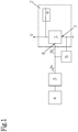
- a semiconductor switching element 1 for example, as an electronic switch in an electrical circuit 2, for example a DC / DC converter, as in FIG Fig.1 indicated, used.
- semiconductor switching elements 1 occur in power electronics, for example in DC / AC converters, AC / DC converters or DC / DC converters for a wide variety of applications, for example in a charger in the kW range, a welding device or an inverter of a photovoltaic system.
- the semiconductor switching element 1 must be switched at a high frequency.
- a standard gate driver 3 which, under the control of a control unit 4, generates a steep-edged driver control voltage V S of a specific frequency for driving the semiconductor switching element 1 at the output.
- the driver control voltage V S is applied to the control terminal 6 of the semiconductor switching element 1 in order to control the flow of current via the semiconductor switching element 1 in accordance with the predetermined switching behavior of the semiconductor switching element 1.
- the gate driver 3 is controlled by a control unit 4, for example by means of pulse width modulation (PWM).
- PWM pulse width modulation
- a ramp generation unit 5 is connected between the control connection 6 and output connection 7, for example an emitter connection in an IGBT or a source connection in a MOSFET, of the semiconductor switching element 1, which ensures that the voltage rise of the rectangular edge of the steep-edged driver control voltage V S is standard Gate driver 3 is reduced.
- the output connection 7 is normally at a reference potential, for example a zero potential. In contrast to the steep edges of the driver control voltage V S , this is intended to generate a transistor control voltage V G with defined rising and falling ramps.
- the electrical energy for operating the ramp generation unit 5 comes directly from the gate driver 3, so that no additional supply voltage input has to be provided for the ramp generation unit 5.
- the ramp generation unit 5 is an additional electrical circuit that loads the gate driver 3 in terms of power (since the gate driver 3 provides the electrical energy for the ramp generation unit 5), but ensures that a standard gate driver 3 can be used and only the disadvantages associated with the steep-edged driver control voltage V S are eliminated. Possible implementations of the ramp generation unit 5 are described below with reference to FIG Fig. 2 and 3 described.
- the basic idea of the ramp generation unit 5 is to apply the driver control voltage V S supplied by the gate driver 3 on the input side to the ramp generation unit 5 and to arrange a transistor T1 on the output side in the ramp generation unit 5, the transistor T1 either from a ramp-shaped voltage (with a rising edge of the driver control voltage V S ) or a ramp-shaped falling voltage (with a falling edge of the driver control voltage V S ), so that a ramp-shaped falling or rising transistor current I 1 flows through the transistor T1.
- the curve shape of the transistor current I 1 specifies the curve shape of the output current I G of the ramp generation unit 5, and thus also the curve shape of the transistor control voltage V G with which the semiconductor switching element 1 is controlled becomes.
- a transistor current I 1 that rises or falls in the form of a ramp then causes an output current I G to rise or fall in the form of a ramp and thus also a transistor control voltage V G to rise or fall in the form of a ramp.
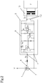
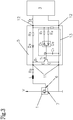
- a signal transmitter 10 with electrical isolation for signal transmission is provided between gate driver 3 and ramp generation unit 5, while in the exemplary embodiment according to Fig. 3 no potential separation is provided and the gate driver 3 is connected directly to the ramp generation unit 5.
- the ramp generation unit 5 is supplied with electrical energy exclusively by the gate driver 3.
- a gate resistor R G and also an inductance L, for example a known multilayer ferrite for filtering EMC interference, can be provided upstream of the control connection 6 of the semiconductor switching element 1 in a known manner.
- any protective circuitry in the ramp generation unit 5, such as diodes, resistors is only discussed if this is important for the function of the ramp generation unit 5 according to the invention. Otherwise it can be assumed that a specialist will recognize the function of the protective circuit.
- the ramp generation unit 5 has input connections 12 and output connections 11. One of the input connections 12 and output connections 11 are connected to one another and to a reference potential, for example a zero potential, in a known manner, which is why an input connection 12 and an output connection will also be referred to in the following.
- the output of the gate driver 3 or the output of the signal transmitter 10 is connected to the input connection 12.
- an input connection 12 is connected to an output connection 11 via a line 8 in which a current limiting resistor R3, and possibly a diode D3, are arranged.
- the ramp generation unit 5 is parallel to the output connection 11 a transistor T1, here a pnp bipolar transistor, is connected.
- the transistor T1 is thus connected between line 8 and the reference potential and thus branches off from line 8.
- a pnp bipolar transistor another type of transistor can of course also be used for the transistor T1.
- the transistor T1 is designed as a known Darlington circuit by means of two transistors, also called Darlington transistor, but this is of no further significance for the invention.
- the Darlington transistor of the Fig. 2 is also generally referred to here as transistor T1.
- the transistor T1 is here with the transistor output connection E, for example an emitter connection, and the transistor input connection C, for example a collector connection, (in the case of a Darlington transistor on the output-side transistor of the Darlington circuit) between the output connections 11 of the ramp generation unit 5 switched.
- the transistor output connection E of the transistor T1 is connected to the control connection 6 of the semiconductor switching element 1, if necessary via the gate resistor R G and the inductance L.
- An RC charging circuit 13 consisting of a capacitor C1 and a resistor R1 or R2, switched. Via the diodes D1, D2 connected in series with a resistor R1, R2, the resistors R1, R2 are switched on depending on the direction of the current.
- the capacitance C1 of the RC charging circuit 13 is connected between the transistor control connection B and the transistor input connection C of the transistor T1 (in the case of a Darlington transistor on the transistor on the input side).
- the RC charging circuit 13 is also connected to the input of the ramp generation unit 5 in that the resistors R1, R2 are connected to the input connection 12 ..
- FIG Fig. 4 shows the ramp generation unit 5 in a simplified manner, and the Figures 5 to 8 showing characteristic signal curves.
- the steep-edged driver control voltage V S of the gate driver 3 is applied to the input terminal 12 of the ramp generation unit 5 ( Fig. 5 ) and an input current I 2 flows from the gate driver 3 into the ramp generation unit 5.
- the driver control voltage V S is also applied to the RC charging circuit 13 connected to the input terminal 12, whereby its capacitor C1 is charged (voltage V R ) until the voltage levels are equal ( Fig. 5 ).
- the current through the RC charging circuit 13 is neglected here.
- a transistor control voltage V G with a flat rising, ramp-shaped edge is applied to the control terminal 6 by the output current I G falling in the form of a ramp, and possibly the gate resistor R G.
- the steeply rising edge of the driver control voltage V S has thus been flattened in a ramp-shaped manner by the ramp generation unit 5. This effect can be precisely set by appropriately dimensioning the RC charging circuit 13.
- the ramp generation unit 5 thus tries to generate a strictly monotonically increasing transistor control voltage V G.
- the current peaks or dips in the current curves of the transistor current I 1 ( Fig. 6 ) and the output current I G ( Fig. 7 ) are a consequence of the well-known Miller effect in the semiconductor switching element 1.
- the Miller effect also causes a brief flattening of the rising and falling edges of the transistor control voltage V G ( Fig. 8 ).
- the steeply falling edge of the driver control voltage V S from the gate driver 3 is flattened by the ramp generation unit 5, as is also shown in FIG Figures 5 to 8 shown.
- the falling transistor current I 1 is in turn branched off from the output current I G , which leads to a ramp-shaped flattening of the falling edge of the transistor control voltage V G.
- Fig. 9 shows a modification of the ramp generation unit 5 according to the invention.
- the transistor T1 is still connected to the output 11 of the ramp generation unit 5 with the transistor output connection E.
- the input connection 12 is no longer directly connected to the line 8, possibly via resistor R3 and diode D3, to the output connection 11.
- a second transistor T2 with the polarity reversed to that of transistor T1, here of the npn type, has its transistor output connection E connected to the transistor output connection E of the first transistor T1 and the transistor input connection C2 of the second transistor T2 is connected to the line 8 connected.
- the transistor control connection B2 of the second transistor T2 is connected to the transistor control connection B of the first transistor T1, whereby the RC charging circuit 13 with the voltage V R is also applied to the transistor control connection B2 of the second transistor T2.
Landscapes
- Engineering & Computer Science (AREA)
- Power Engineering (AREA)
- Power Conversion In General (AREA)
- Electronic Switches (AREA)
Description
- Die gegenständliche Erfindung betrifft eine Schaltungsanordnung zum Ansteuern eines Halbleiterschaltelements, wobei ein Gate-Treiber eine steilflankige Steuerspannung für das Halbleiterschaltelement erzeugt und der Gate-Treiber mit dem Steueranschluss des Halbleiterschaltelements verbunden ist.
- Zum Schalten von aktiven Halbleiterschaltelementen, insbesondere Transistoren, wie beispielsweise ein Bipolartransistor mit isolierter Gate-Elektrode (IGBT) oder ein Metall-Oxid-Halbleiter-Feldeffekttransistor (MOSFET), werden sogenannte Gate-Treiber verwendet, die an den Steueranschluss des Halbleiterschaltelements (Gate-Anschluss beim IGBT und beim MOSFET) angeschlossen werden und die eine Treiber-Steuerspannung erzeugen, um den Stromfluss über das Halbleiterschaltelement zu kontrollieren. Ein herkömmlicher Standard Gate-Treiber erzeugt als Treiber-Steuerspannung eine steilflankige Rechteckspannung. Dadurch wird das Halbleiterschaltelement ohne Rücksicht auf das jeweilige Schaltverhalten angesteuert. Dies kann zu unerwünschten Oszillationen, Probleme durch hochfrequente elektromagnetische Abstrahlung, bis hin zur Zerstörung des Halbleiterschaltelements führen. Dafür sind solche Standard Gate-Treiber als Hardware Bausteine kommerziell günstig erhältlich. Die
JP 3 066754 B2 DE 10 2012 218 284 A1 zeigen beispielsweise eine Schaltung zum Ansteuern eines Halbleiterschaltelements, wobei ein unerwünschtes Schalten des Halbleiterschalters verhindert werden soll. - Im Stand der Technik finden sich bereits einige Lösungsansätze, um die genannte Probleme solcher Standard Gate-Treiber zu beseitigen bzw. zu reduzieren.
- In der
WO 2012/007558 A1 wird ein Verfahren und eine Anordnung zur Ansteuerung von Power-MOS-Transistoren offenbart. Hierbei wird der Transistor zum Ausschalten mit einer linear fallenden und zum Einschalten mit einer linear ansteigenden Steuerspannung angesteuert - also jeweils mit einer Spannungsrampe anstatt der steilflankigen Treiber-Steuerspannung. Schaltungstechnisch wird das durch einen Impedanzwandler mit Verstärker, Stromquellen und einem Kondensator erreicht, also durch eine aufwendige elektrische Schaltung. - Ebenso wurde bereits vorgeschlagen, die Spannungsflanken der Steuerspannung des Halbleiterschalters durch eine geschlossene Regelschleife aktiv zu regeln, wie z.B. in Lobsiger Y. et al., "Closed Loop di/dt & dv/dt Control and Dead Time Minimization of IGBTs in Bridge Leg Configuration", Proceedings 14th IEEE Workshop an Control an Modeling for Power Electronics (COMPEL 2013), Salt Lake City, USA, June 23-26, 2013. Eine solche aktive Regelung ist aber für einen Gate-Treiber sowohl hardware- als auch softwaremäßig aufwendig.
- Beiden oben genannten Konzepten ist zudem gemein, dass beide eine komplett neue Schaltung für einen Gate-Treiber vorschlagen, die als Hardware, eventuell mit geeigneter Steuersoftware, zu entwickeln und umzusetzen ist. Die vorhandenen kostengünstigen Standard Gate-Treiber Bausteine sind damit nicht mehr einsetzbar, sondern müssen durch neu entwickelte ersetzte werden.
- Die
JP 2003 125574 A EP 0 053 709 A2 zeigt eine Schaltung zum Unterdrücken positiver Flanken. - Es ist nun eine Aufgabe der gegenständlichen Erfindung, die oben genannten Probleme beim Schalten von Halbleiterschaltelementen mit herkömmlichen Gate-Treibern auf einfache und kostengünstige Weise zu reduzieren.
- Diese Aufgabe wird erfindungsgemäß dadurch gelöst, dass der Steueranschluss des Halbleiterschaltelements über eine Rampenerzeugungseinheit mit dem Ausgangsanschluss des Halbleiterschaltelements verbunden ist und die Rampenerzeugungseinheit zur Erzeugung einer Transistor-Steuerspannung am Ausgang der Rampenerzeugungseinheit die steil steigenden und fallenden Flanken der Treiber-Steuerspannung rampenförmig abflacht, die Energieversorgung der Rampenerzeugungseinheit durch den Gate-Treiber erfolgt und in der Rampenerzeugungseinheit ausgangsseitig einen Transistor angeordnet ist, der von einer rampenförmig ansteigenden oder abfallenden Spannung gesteuert ist, wodurch über den Transistor ein rampenförmig fallender oder steigender Transistorstrom fließt. Damit kann für die Ansteuerung des Halbleiterschaltelements wie bisher ein Standard Gate-Treiber verwendet werden, wobei die Nachteile der steilflankigen Treiber-Steuerspannung durch die Abflachung der steilen Flanken in der Rampenerzeugungseinheit vermindert werden. Die Rampenerzeugungseinheit ist eine einfache elektrische Zusatzbeschaltung und bedarf keiner aufwendigen Überarbeitung des Gate-Treibers, sondern kann einfach zwischen Gate-Treiber und Halbleiterschaltelement hinzugefügt werden, was es ermöglicht elektrische Schaltungen unter Verwendung von elektrischen Standardbauteilen sehr einfach zu adaptieren.
- Zur Potentialtrennung kann zwischen Gate-Treiber und Rampenerzeugungseinheit auch ein Signalübertrager geschaltet sein.
- Erfindungsgemäß ist in der Rampenerzeugungseinheit ausgangsseitig ein Transistor angeordnet, der von einer rampenförmig ansteigenden Spannung oder einer rampenförmig abfallenden Spannung gesteuert wird, wodurch über den Transistor ein rampenförmig fallender oder steigender Transistorstrom fließt. Der rampenförmige Strom über den Transistor zweigt vom Ausgangsstrom der Rampenerzeugungseinheit damit ab, wodurch auch der Ausgangsstrom rampenförmig ansteigt bzw. abfällt. Das bewirkt dann eine Transistor-Steuerspannung am Ausgang der Rampenerzeugungseinheit mit rampenförmig steigenden und fallenden Flanken - die steilen Flanken der Treiber-Steuerspannung wurden damit abgeflacht.
- Die rampenförmige Spannung zum Ansteuern des Transistors wird vorteilhafter Weise dadurch erzeugt, dass in der Rampenerzeugungseinheit ein erster Transistor und eine RC-Ladeschaltung mit einem Widerstand und einer Kapazität vorgesehen sind, wobei der Transistor-Ausgangsanschluss des ersten Transistors mit dem Ausgangsanschluss der Rampenerzeugungseinheit verbunden ist, die RC-Ladeschaltung über den Widerstand mit dem Eingangsanschluss der Rampenerzeugungseinheit verbunden ist und die Kapazität der RC-Ladeschaltung mit dem Transistor-Steueranschluss des ersten Transistors verbunden ist. Das lässt sich mit elektrischen Standardbauteilen auf einfachste Weise realisieren. Durch einfache Dimensionierung der RC-Ladeschaltung kann darüber hinaus auch die Wirkung der Abflachung der steilen Flanken der Treiber-Steuerspannung einfach kontrolliert werden.
- In einer anderen Ausgestaltung der Erfindung, sind in der Rampenerzeugungseinheit ein erster Transistor, ein zweiter Transistor und eine RC-Ladeschaltung mit einem Widerstand und einer Kapazität vorgesehen, wobei der Transistor-Ausgangsanschluss des ersten Transistors und des zweiten Transistors miteinander und mit dem Ausgangsanschluss der Rampenerzeugungseinheit verbunden sind, der Transistor-Steueranschluss des zweiten Transistors mit dem Eingangsanschluss der Rampenerzeugungseinheit verbunden ist, die RC-Ladeschaltung über den Widerstand mit dem Eingangsanschluss der Rampenerzeugungseinheit verbunden ist und die Kapazität der RC-Ladeschaltung mit dem Transistor-Steueranschluss des ersten Transistors und des zweiten Transistors verbunden ist. Diese Schaltung hat den Vorteil, dass bei vertretbarem zusätzlichen schaltungstechnischen Aufwand durch den zusätzlichen Transistor, die leistungsmäßige Belastung des Gate-Treibers durch die Rampenerzeugungseinheit verringert werden kann.
- Die gegenständliche Erfindung wird nachfolgend unter Bezugnahme auf die
Figuren 1 bis 14 näher erläutert, die beispielhaft, schematisch und nicht einschränkend vorteilhafte Ausgestaltungen der Erfindung zeigen. Dabei zeigt -
Fig.1 eine erfindungsgemäße Schaltungsanordnung zum Ansteuern eines Halbleiterschaltelements, -
Fig.2 eine Ausgestaltung der erfindungsgemäßen Rampenerzeugungseinheit, -
Fig.3 eine alternative Ausgestaltung der erfindungsgemäßen Rampenerzeugungseinheit, -
Fig.4 eine vereinfachte Darstellung einer erfindungsgemäßen Rampenerzeugungseinheit, -
Fig.5 bis 8 Kurven von charakteristischen Strömen und Spannungen der Rampenerzeugungseinheit, -
Fig.9 eine weitere Ausgestaltung der erfindungsgemäßen Rampenerzeugungseinheit, -
Fig.10 bis 14 Kurven von charakteristischen Strömen und Spannungen dieser Rampenerzeugungseinheit. - Wie in
Fig.1 schematisch dargestellt, wird ein Halbleiterschaltelement 1 beispielsweise als elektronischer Schalter in einer elektrischen Schaltung 2, z.B. ein DC/DC-Konverter, wie inFig.1 angedeutet, verwendet. Insbesondere kommen solche Halbleiterschaltelemente 1 in Leistungselektronik vor, z.B. in DC/AC-Wandlern, AC/DC-Wandlern oder DC/DC-Wandlern für verschiedenste Anwendungen, beispielsweise in einem Ladegerät im kW-Bereich, einem Schweißgerät oder einem Wechselrichter einer Photovoltaikanlage. Gemein ist solchen leistungselektronischen Schaltungen, dass das Halbleiterschaltelement 1 mit hoher Frequenz geschaltet werden muss. Zum Schalten des Halbleiterschaltelements 1 wird ein Standard Gate-Treiber 3 verwendet, der am Ausgang unter Kontroller einer Steuereinheit 4 eine steilflankige Treiber-Steuerspannung VS einer bestimmten Frequenz zum Ansteuern des Halbleiterschaltelements 1 erzeugt. Die Treiber-Steuerspannung VS wird an den Steueranschluss 6 des Halbleiterschaltelements 1 angelegt, um den Stromfluss über das Halbleiterschaltelement 1 gemäß dem vorgegebenen Schaltverhalten des Halbleiterschaltelements 1 zu kontrollieren. Eingangsseitig wird der Gate-Treiber 3 von einer Steuereinheit 4, z.B. mittels Pulsweitenmodulation (PWM), angesteuert. Solche leistungselektronischen Schaltungen 2 sind hinlänglich bekannt, weshalb hier nicht näher darauf eingegangen wird. - Zwischen Steueranschluss 6 und Ausgangsanschluss 7, z.B. ein Emitteranschluss bei einem IGBT oder ein Source-Anschluss bei einem MOSFET, des Halbleiterschaltelements 1 ist erfindungsgemäß eine Rampenerzeugungseinheit 5 geschaltet, die dafür sorgt, dass der Spannungsanstieg der Rechteckflanke der steilflankigen Treiber-Steuerspannung VS vom Standard Gate-Treiber 3 reduziert wird. Der Ausgangsanschluss 7 liegt normalerweise auf einem Referenzpotential, z.B. einem Nullpotential. Damit soll, im Gegensatz zu den steilen Flanken der Treiber-Steuerspannung VS, eine Transistor-Steuerspannung VG mit definierten steigenden und fallenden Rampen erzeugt werden. Die elektrische Energie zum Betreiben der Rampenerzeugungseinheit 5 kommt dabei direkt vom Gate-Treiber 3, sodass für die Rampenerzeugungseinheit 5 kein zusätzlicher Versorgungsspannungseingang vorzusehen ist. Die Rampenerzeugungseinheit 5 ist eine elektrische Zusatzbeschaltung, die den Gate-Treiber 3 zwar leistungsmäßig belastet (da der Gate-Treiber 3 die elektrische Energie für die Rampenerzeugungseinheit 5 zur Verfügung stellt), jedoch dafür sorgt, dass ein Standard Gate-Treiber 3 verwendet werden kann und nur die mit der steilflankigen Treiber-Steuerspannung VS verbundenen Nachteile eliminiert werden. Mögliche Implementierungen der Rampenerzeugungseinheit 5 werden im Nachfolgenden unter Bezugnahme auf die
Fig.2 und3 beschrieben. - Die Grundidee der Rampenerzeugungseinheit 5 liegt darin, an die Rampenerzeugungseinheit 5 eingangsseitig die vom Gate-Treiber 3 gelieferte Treiber-Steuerspannung VS anzulegen und in der Rampenerzeugungseinheit 5 ausgangsseitig einen Transistor T1 anzuordnen, wobei der Transistor T1 entweder von einer rampenförmig ansteigenden Spannung (bei einer steigenden Flanke der Treiber-Steuerspannung VS) oder einer rampenförmig abfallenden Spannung (bei einer fallenden Flanke der Treiber-Steuerspannung VS) gesteuert wird, sodass über den Transistor T1 ein rampenförmig fallender oder steigender Transistorstrom I1 fließt. Nachdem der Transistor T1 mit dem Ausgang 11 der Rampenerzeugungseinheit 5 verbunden ist, gibt die Kurvenform des Transistorstromes I1 die Kurvenform des Ausgangsstromes IG der Rampenerzeugungseinheit 5 vor, und damit auch die Kurvenform der Transistor-Steuerspannung VG, mit der das Halbleiterschaltelement 1 angesteuert wird. Ein rampenförmig steigender oder fallender Transistorstrom I1 bewirkt dann einen rampenförmig steigenden oder fallenden Ausgangsstrom IG und damit auch eine rampenförmig steigende oder fallende Transistor-Steuerspannung VG.
- Im Ausführungsbeispiel nach
Fig.2 ist zwischen Gate-Treiber 3 und Rampenerzeugungseinheit 5 ein Signalübertrager 10 mit Potentialtrennung für die Signalübertragung vorgesehen, während im Ausführungsbeispiel nachFig.3 keine Potentialtrennung vorgesehen ist und der Gate-Treiber 3 direkt an die Rampenerzeugungseinheit 5 angeschlossen ist. In beiden Fällen wird die Rampenerzeugungseinheit 5 ausschließlich vom Gate-Treiber 3 mit elektrischer Energie versorgt. Vor dem Steueranschluss 6 des Halbleiterschaltelements 1 kann in bekannter Weise ein Gate-Widerstand RG und auch eine Induktivität L, beispielsweise ein bekanntes Multilayerferrit zur Filterung von EMV-Störungen, vorgesehen sein. In der nachfolgenden Beschreibung wird auf allfällige Schutzbeschaltung in der Rampenerzeugungseinheit 5, wie z.B. Dioden, Widerstände, nur eingegangen, sofern diese für die erfindungsgemäße Funktion der Rampenerzeugungseinheit 5 von Bedeutung ist. Ansonsten kann vorausgesetzt werden, dass ein Fachmann die Funktion der Schutzbeschaltung erkennt. - Die Rampenerzeugungseinheit 5 weist Eingangsanschlüsse 12 und Ausgangsanschlüsse 11 auf. Einer der Eingangsanschlüsse 12 und Ausgangsanschlüsse 11 sind in bekannter Weise miteinander und mit einem Referenzpotential, z.B. einem Nullpotential, verbunden, weshalb in weitere Folge auch von einem Eingangsanschluss 12 und einem Ausgangsanschluss gesprochen wird. An den Eingangsanschluss 12 wird der Ausgang des Gate-Treibers 3, bzw. der Ausgang des Signalübertragers 10, geschaltet. In der Rampenerzeugungseinheit 5 ist in den gezeigten Ausführungsbeispielen nach den
Figuren 2 und3 ein Eingangsanschluss 12 über eine Leitung 8, in der ein Strombegrenzungswiderstand R3, und gegebenenfalls eine Diode D3, angeordnet sind, mit einem Ausgangsanschluss 11 verbunden. In der Rampenerzeugungseinheit 5 ist parallel zum Ausgangsanschluss 11 der Rampenerzeugungseinheit 5 ein Transistor T1, hier ein pnp-Bipolartransistor, geschaltet. Der Transistor T1 ist damit zwischen Leitung 8 und dem Referenzpotential geschaltet und zweigt damit von der Leitung 8 ab. Anstelle eines pnp-Bipolartransistors kann natürlich auch ein anderer Transistortyp für den Transistor T1 verwendet werden. - In
Fig.2 ist der Transistor T1 als bekannte Darlington-Schaltung mittels zwei Transistoren, auch Darlington-Transistor genannt, ausgeführt, was für die Erfindung aber keine weitere Bedeutung hat. Der Darlington-Transistor derFig.2 wird hier ebenfalls allgemein als Transistor T1 bezeichnet. - Der Transistor T1 ist hier mit dem Transistor-Ausgangsanschluss E, z.B. ein EmitterAnschluss, und dem Transistor-Eingangsanschluss C, z.B. ein Kollektor-Anschluss, (bei einem Darlington-Transistor am ausgangsseitigen Transistor der Darlington-Schaltung) zwischen die Ausgangsanschlüsse 11 der Rampenerzeugungseinheit 5 geschaltet. Der Transistor-Ausgangsanschluss E des Transistors T1 wird dabei mit dem Steueranschluss 6 des Halbleiterschaltelements 1 verbunden, gegebenenfalls über den Gate-Widerstand RG und die Induktivität L.
- An den Transistor-Steueranschluss B, z.B. ein Basis-Anschluss, des Transistors T1 (bei einem Darlington-Transistor am eingangsseitigen Transistor der Darlington-Schaltung) wird eine RC-Ladeschaltung 13 bestehend aus einer Kapazität C1 und einem Widerstand R1, bzw. R2, geschaltet. Über die jeweils in Serie zu einem Widerstand R1, R2 geschalteten Dioden D1, D2 werden die Widerstände R1, R2 in Abhängigkeit von der Stromrichtung zugeschaltet. Die Kapazität C1 der RC-Ladeschaltung 13 ist dabei zwischen Transistor-Steueranschluss B und Transistor-Eingangsanschluss C des Transistors T1 (bei einem Darlington Transistor am eingangsseitigen Transistor) geschaltet. Die RC-Ladeschaltung 13 ist außerdem an den Eingang der Rampenerzeugungseinheit 5 geschaltet, indem die Widerstände R1, R2 mit dem Eingangsanschluss 12 verbunden werden..
- Die Funktion der Rampenerzeugungseinheit 5 wird nun unter Bezugnahme auf die
Fig.4 , die die Rampenerzeugungseinheit 5 vereinfacht zeigt, und dieFiguren 5 bis 8 , die charakteristische Signalverläufe zeigen, beschrieben. - An den Eingangsanschluss 12 der Rampenerzeugungseinheit 5 liegt die steilflankige Treiber- Steuerspannung VS des Gate-Treibers 3 an (
Fig.5 ) und es fließt vom Gate-Treiber 3 ein Eingangsstrom I2 in die Rampenerzeugungseinheit 5. Dadurch liegt die Treiber- Steuerspannung VS auch an die mit dem Eingangsanschluss 12 verbundene RC-Ladeschaltung 13 an, wodurch deren Kondensator C1 aufgeladen wird (Spannung VR), bis die Spannungsniveaus angeglichen sind (Fig.5 ). Die ansteigende Spannung VR über den Kondensator C1, die an den Transistor-Steueranschluss B des Transistors T1 angelegt ist, steuert den pnp-Typ Transistor T1, was einen rampenförmig abfallenden Strom I1 über den Transistor T1 bewirkt (Fig.6 ). Der Transistorstrom I1 über den Transistor T1 zweigt vom Ausgangsanschluss 11 der Rampenerzeugungseinheit 5 ab, wodurch sich der Ausgangsstrom IG der Rampenerzeugungseinheit 5 aus der Differenz von Eingangsstrom I2 und dem Transistorstrom I1 ergibt, also IG=I2-I1. Der Strom über die RC-Ladeschaltung 13 wird hier vernachlässigt. Am Halbleiterschaltelement 1 wird damit durch den rampenförmig abfallenden Ausgangsstrom IG, und gegebenenfalls dem Gate-Widerstand RG, an den Steueranschluss 6 eine Transistor-Steuerspannung VG mit flacher steigender, rampenförmiger Flanke angelegt. Die steil ansteigende Flanke der Treiber- Steuerspannung VS wurde damit durch die Rampenerzeugungseinheit 5 rampenförmig abgeflacht. Durch entsprechende Dimensionierung der RC-Ladeschaltung 13 lässt sich diese Wirkung genau einstellen. - Die Rampenerzeugungseinheit 5 versucht damit, eine streng monoton steigende Transistor-Steuerspannung VG zu generieren. Die Stromspitzen bzw. Einbrüche in den Stromverläufen des Transistorstromes I1 (
Fig.6 ) und des Ausgangsstromes IG (Fig.7 ) sind eine Folge des bekannten Miller-Effekts im Halbleiterschaltelement 1. Ebenso bewirkt der Miller-Effekt eine kurzfristige Abflachung der steigenden und fallen Flanken der Transistor-Steuerspannung VG (Fig.8 ). - Analog wird die steil abfallende Flanke der Treiber-Steuerspannung VS vom Gate-Treiber 3 durch die Rampenerzeugungseinheit 5 abgeflacht, wie ebenfalls in den
Figuren 5 bis 8 dargestellt. Der abfallende Transistorstrom I1 wird dabei wiederum vom Ausgangsstrom IG abgezweigt, was zu einer rampenförmigen Abflachung der fallenden Flanke der Transistor-Steuerspannung VG führt. -
Fig. 9 zeigt eine Abwandlung der erfindungsgemäßen Rampenerzeugungseinheit 5. Hier ist der Transistor T1 nachwievor mit dem Transistor-Ausgangsanschluss E auf den Ausgang 11 der Rampenerzeugungseinheit 5 geschaltet. Der Eingangsanschluss 12 ist hier aber nicht mehr direkt mit der Leitung 8, gegebenenfalls über Widerstand R3 und Diode D3, mit dem Ausgangsanschluss 11 verbunden. Ein zweiter Transistor T2 mit zum Transistor T1 umgekehrten Polarität, hier vom npn-Typ, ist mit dessen Transistor-Ausgangsanschluss E mit dem Transistor-Ausgangsanschluss E des ersten Transistors T1 verbunden und der Transistor-Eingangsanschluss C2 des zweiten Transistors T2 ist mit der Leitung 8 verbunden. Der Transistor-Steueranschluss B2 des zweiten Transistors T2 ist mit dem Transistor-Steueranschluss B des ersten Transistors T1 verbunden, womit auch am Transistor-Steueranschluss B2 des zweiten Transistors T2 die RC-Ladeschaltung 13 mit der Spannung VR anliegt. - Die Wirkung dieser Schaltung ist identisch zur oben beschriebenen Ausgestaltung der Rampenerzeugungseinheit 5 nach
Fig.2 oder3 und es wird wieder eine rampenförmige Abflachung der Spannungsflanken der Treiber-Steuerspannung VS erzeugt, wie insbesondere aus denFig. 10 bis 14 hervorgeht. - Der einzige Unterschied besteht darin, dass nun die steigende rampenförmige Flanke der Transistor-Steuerspannung VG vom zweiten Transistor T2 generiert wird und die fallende rampenförmige Flanke der Transistor-Steuerspannung VG vom ersten Transistor T1.
- Der Vorteil dieser Schaltung nach
Fig.9 liegt darin, dass der Standard Gate-Treiber 3 von dieser Schaltung weniger belastet wird, da für die steigende Flanke der Ausgangsstrom IG gleich dem Eingangsstrom I2, der auch dem Strom über den zweiten Transistor T2 entspricht, ist. Diesen Vorteil erkauft man sich aber durch einen zusätzlichen Bauteil in Form des zweiten Transistors T2.
Claims (5)
- Schaltungsanordnung zum Ansteuern eines Halbleiterschaltelements (1), wobei ein Gate-Treiber (3) eine steilflankige Treiber-Steuerspannung (Vs) für das Halbleiterschaltelement (1) erzeugt und der Gate-Treiber (3) mit dem Steueranschluss (6) des Halbleiterschaltelements (1) verbunden ist, wobei Steueranschluss (6) des Halbleiterschaltelements (1) über eine Rampenerzeugungseinheit (5) mit dem Ausgangsanschluss (7) des Halbleiterschaltelements (1) verbunden ist, die Rampenerzeugungseinheit (5) zur Erzeugung einer Transistor-Steuerspannung (VG) am Ausgang der Rampenerzeugungseinheit (5) die steil steigenden und fallenden Flanken der Treiber-Steuerspannung (Vs) rampenförmig abflacht und die Energieversorgung der Rampenerzeugungseinheit (5) durch den Gate-Treiber (3) erfolgt, wobei in der Rampenerzeugungseinheit (5) ausgangsseitig ein Transistor (T1, T2) angeordnet ist, der von einer rampenförmig ansteigenden oder abfallenden Spannung (VR) gesteuert ist, wodurch über den Transistor (T1 ,T2) ein rampenförmig fallender oder steigender Transistorstrom (I1) fließt, und wobei in der Rampenerzeugungseinheit (5) ein erster Transistor (T1) und eine RC-Ladeschaltung (13) mit einem Widerstand (R1, R2) und einem Kondensator (C1) vorgesehen sind, wobei der Transistor-Ausgangsanschluss (E) des ersten Transistors (T1) mit dem Ausgangsanschluss (11) der Rampenerzeugungseinheit (5) verbunden ist, der Widerstand (R1, R2) der RC-Ladeschaltung (13) zwischen dem Eingangsanschluss (12) der Rampenerzeugungseinheit (5) und dem Transistor-Steueranschluss (B) des ersten Transistors (T1) geschalten ist und der Kondensator (C1) der RC-Ladeschaltung (13) mit dem Transistor-Steueranschluss (B) des ersten Transistors (T1) verbunden ist.
- Schaltungsanordnung nach Anspruch 1, wobei zwischen Gate-Treiber (3) und Rampenerzeugungseinheit (5) ein Signalübertrager (10) geschaltet ist.
- Schaltungsanordnung nach Anspruch 1 oder 2, wobei in der Rampenerzeugungseinheit (5) ein zweiter Transistor (T2), mit zum ersten Transistor T1 umgekehrten Polarität vorgesehen sind, wobei der Transistor-Ausgangsanschluss (E) des zweiten Transistors (T2) mit dem Transistor-Ausgangsanschluss des ersten Transistors (T1) verbunden ist, sodass der erste Transistor (T1) und der zweite Transistor (T2) in Serie geschaltet sind, und der Kondensator (C1) der RC-Ladeschaltung (13) mit dem Transistor-Steueranschluss (B2) des zweiten Transistors (T2) verbunden ist.
- Verfahren zum Ansteuern eines Halbleiterschaltelements (1) mit einem Gate-Treiber (3), der mit einem Steueranschluss (6) des Halbleiterschaltelements (1) verbunden wird und der eine steilflankige Treiber-Steuerspannung (VS) erzeugt, wobei vom Gate-Treiber (3) ein Eingangsstrom (I2) in eine Rampenerzeugungseinheit (5) fließt und der Gate-Treiber (3) die Rampenerzeugungseinheit (5) mit Energie versorgt, wobei in der Rampenerzeugungseinheit (5) vom Eingangsstrom (I2) ein rampenförmiger Strom (I1) abgezweigt wird, um einen rampenförmigen Ausgangsstrom (IG) der Rampenerzeugungseinheit (5) zu erzeugen, wobei der rampenförmige Ausgangsstrom (IG) in den Steueranschluss (6) des Halbleiterschaltelements (1) fließt und eine Transistor-Steuerspannung (VG) mit rampenförmig steigenden oder fallenden Flanken bewirkt, wobei in der Rampenerzeugungseinheit (5) eine rampenförmig ansteigende oder abfallenden Spannung (VR) an einen Transistor-Steueranschluss (B) eines ersten Transistors (T1) angelegt wird und die Spannung (VR) den ersten Transistor (T1) steuert und wobei die Transistor-Steuerspannung (VG) mittels einer RC-Ladeschaltung (13) aus der Treiber-Steuerspannung (VS) erzeugt wird.
- Verfahren nach Anspruch 4, wobei die an einem Kondensator (C1) der RC-Ladeschaltung (13) anliegende Spannung (VR) jeweils an einen Transistor-Steueranschluss (B, B2) von zwei in Serie geschalteten Transistoren (T1, T2) angelegt wird, wobei die Transistoren (T1, T2) über deren Transistor-Ausgangsanschlüsse (E) miteinander und mit dem Steueranschluss (6) des Halbleiterschaltelements (1) verbunden werden.
Applications Claiming Priority (1)
| Application Number | Priority Date | Filing Date | Title |
|---|---|---|---|
| ATA50341/2014A AT515848B1 (de) | 2014-05-15 | 2014-05-15 | Schaltungsanordnung und Verfahren zum Ansteuern eines Halbleiterschaltelements |
Publications (2)
| Publication Number | Publication Date |
|---|---|
| EP2945288A1 EP2945288A1 (de) | 2015-11-18 |
| EP2945288B1 true EP2945288B1 (de) | 2021-02-24 |
Family
ID=53199799
Family Applications (1)
| Application Number | Title | Priority Date | Filing Date |
|---|---|---|---|
| EP15167507.1A Active EP2945288B1 (de) | 2014-05-15 | 2015-05-13 | Schaltungsanordnung und verfahren zum ansteuern eines halbleiterschaltelements |
Country Status (4)
| Country | Link |
|---|---|
| US (1) | US9729136B2 (de) |
| EP (1) | EP2945288B1 (de) |
| CN (1) | CN105119589B (de) |
| AT (1) | AT515848B1 (de) |
Cited By (1)
| Publication number | Priority date | Publication date | Assignee | Title |
|---|---|---|---|---|
| EP3846344A1 (de) * | 2019-12-30 | 2021-07-07 | Iolo AG | Intelligenter taster für eine gebäudeinstallation |
Families Citing this family (3)
| Publication number | Priority date | Publication date | Assignee | Title |
|---|---|---|---|---|
| DE102017218305A1 (de) * | 2017-10-13 | 2019-04-18 | Conti Temic Microelectronic Gmbh | Verfahren zum Steuern einer Halbleiterbrücke eines elektrisch betreibbaren Motors mittels eines Rampensignals, Steuerungseinrichtung sowie Anordnung |
| CN116982260A (zh) * | 2021-03-19 | 2023-10-31 | 罗姆股份有限公司 | 栅极驱动电路 |
| JPWO2025022733A1 (de) * | 2023-07-25 | 2025-01-30 |
Family Cites Families (24)
| Publication number | Priority date | Publication date | Assignee | Title |
|---|---|---|---|---|
| DE3169198D1 (en) * | 1980-12-04 | 1985-04-11 | Siemens Ag | Circuitry for driving at least one power fet |
| US4540893A (en) * | 1983-05-31 | 1985-09-10 | General Electric Company | Controlled switching of non-regenerative power semiconductors |
| EP0153423B1 (de) * | 1984-02-20 | 1988-02-10 | HONEYWELL BULL ITALIA S.p.A. | Treiberschaltung für einen Leistungs-FET |
| JP3066754B2 (ja) * | 1988-10-31 | 2000-07-17 | 富士電機株式会社 | ゲート駆動回路 |
| JPH0366754A (ja) | 1989-08-04 | 1991-03-22 | Kao Corp | ポリアミド樹脂用溶融粘度低下剤 |
| DE19523096A1 (de) * | 1995-06-26 | 1997-01-02 | Abb Management Ag | Stromrichterschaltungsanordnung |
| JP3623181B2 (ja) * | 2001-08-27 | 2005-02-23 | オリジン電気株式会社 | 高電圧半導体スイッチ装置および高電圧発生装置 |
| JP3767450B2 (ja) * | 2001-10-11 | 2006-04-19 | 富士電機デバイステクノロジー株式会社 | 絶縁ゲートトランジスタの駆動回路および電力変換装置と電力用半導体モジュール |
| US6784624B2 (en) * | 2001-12-19 | 2004-08-31 | Nicholas Buonocunto | Electronic ballast system having emergency lighting provisions |
| JP4082672B2 (ja) * | 2003-03-06 | 2008-04-30 | 株式会社デンソー | 電気絶縁型スイッチング素子駆動回路 |
| KR100560490B1 (ko) * | 2003-10-16 | 2006-03-13 | 삼성에스디아이 주식회사 | 플라즈마 디스플레이 패널의 구동장치 및 구동방법 |
| FR2874767B1 (fr) * | 2004-08-27 | 2006-10-20 | Schneider Toshiba Inverter | Dispositif de commande d'un transistor de puissance |
| US20080054984A1 (en) * | 2006-08-31 | 2008-03-06 | International Rectifier Corporation | High voltage gate driver ic with ramp driver |
| US8199537B2 (en) * | 2009-02-19 | 2012-06-12 | Iwatt Inc. | Detecting light load conditions and improving light load efficiency in a switching power converter |
| CN101710794B (zh) * | 2009-12-17 | 2015-09-02 | 北京中星微电子有限公司 | 完全能量转换模式下的交流-直流反激转换器及其环路补偿方法 |
| US8629630B2 (en) * | 2010-05-25 | 2014-01-14 | Green Solution Technology Co., Ltd. | LED driving circuit and control circuit |
| KR20130041941A (ko) | 2010-07-15 | 2013-04-25 | 첸트룸 미크로엘렉트로닉 드레스덴 악치엔게젤샤프트 | 파워-모스-트랜지스터 구동 제어 방법 및 장치 |
| DE102011079552B4 (de) * | 2011-07-21 | 2014-05-08 | Siemens Aktiengesellschaft | Schaltungsanordnung zum Schalten eines Stromes und Verfahren zum Betreiben eines Halbleiter-Leistungsschalters |
| US9143044B2 (en) * | 2011-09-13 | 2015-09-22 | Futurewei Technologies, Inc. | Apparatus and method for pulse width modulation control for switching power converters |
| CN103023282B (zh) * | 2011-09-23 | 2016-03-30 | 南京博兰得电子科技有限公司 | 一种隔离驱动电路 |
| DE102012218284A1 (de) * | 2012-10-08 | 2014-04-10 | Robert Bosch Gmbh | Treibereinheit zum Ansteuern einer Transistor-Halbbrücke und DC-DC-Wandler |
| JP5469228B1 (ja) * | 2012-10-22 | 2014-04-16 | 三菱電機株式会社 | スイッチ素子駆動装置 |
| GB2511334A (en) * | 2013-02-28 | 2014-09-03 | Control Tech Ltd | Drive circuit for power transistor |
| US9071245B2 (en) * | 2013-04-24 | 2015-06-30 | Hamilton Sundstrand Corporation | Solid state power controller gate control |
-
2014
- 2014-05-15 AT ATA50341/2014A patent/AT515848B1/de active
-
2015
- 2015-05-13 EP EP15167507.1A patent/EP2945288B1/de active Active
- 2015-05-14 US US14/712,128 patent/US9729136B2/en active Active
- 2015-05-15 CN CN201510495693.0A patent/CN105119589B/zh active Active
Non-Patent Citations (1)
| Title |
|---|
| None * |
Cited By (1)
| Publication number | Priority date | Publication date | Assignee | Title |
|---|---|---|---|---|
| EP3846344A1 (de) * | 2019-12-30 | 2021-07-07 | Iolo AG | Intelligenter taster für eine gebäudeinstallation |
Also Published As
| Publication number | Publication date |
|---|---|
| EP2945288A1 (de) | 2015-11-18 |
| AT515848B1 (de) | 2020-09-15 |
| CN105119589A (zh) | 2015-12-02 |
| CN105119589B (zh) | 2018-04-27 |
| US20150333749A1 (en) | 2015-11-19 |
| AT515848A1 (de) | 2015-12-15 |
| US9729136B2 (en) | 2017-08-08 |
Similar Documents
| Publication | Publication Date | Title |
|---|---|---|
| DE102018126779B4 (de) | Gate-Treiber-Schaltung mit Spannungsinvertierung für einen Leistungshalbleiterschalter | |
| DE102019102311A1 (de) | Gate-Treiber-Schaltung mit Spannungsinvertierung für einen Leistungshalbleiterschalter | |
| EP1620947A2 (de) | Betrieb einer halbbrücke, insbesondere einer feldeffekttransistor-halbbrücke | |
| EP1715582B1 (de) | Schaltungsanordnung zur Ansteuerung eines elektrischen Leistungsschalters auf hohem Spannungspotenzial | |
| WO2018091145A1 (de) | Ansteuerschaltung | |
| DE102014202643A1 (de) | Halbleitervorrichtungs-Ansteuerschaltung und Halbleitervorrichtungs-Ansteuereinheit | |
| AT515848B1 (de) | Schaltungsanordnung und Verfahren zum Ansteuern eines Halbleiterschaltelements | |
| EP3316463A1 (de) | Ändern eines schaltzustands einer schalt-halbbrücke | |
| EP1050951B1 (de) | Schaltungsanordnung für eine getaktete Stromversorgung | |
| EP2744110A1 (de) | Ansteuerschaltung und Verfahren zur Ansteuerung eines Leistungshalbleiterschalters | |
| DE102017208187B4 (de) | Elektronisches Modul sowie Kraftfahrzeug und Verfahren zum Begrenzen eines Eingangsstroms während eines Einschaltvorgangs des Moduls | |
| DE102016220679A1 (de) | Gleichspannungswandler und Verfahren zur Ansteuerung eines Gleichspannungswandlers | |
| EP3529102B1 (de) | Gleichspannungswandler und verfahren zum betrieb eines gleichspannungswandlers | |
| DE102012200234B4 (de) | Verfahren und Steuereinrichtung zur Steuerung der Ausschaltgeschwindigkeit eines Halbleiterschalters | |
| EP2783464B1 (de) | Elektronischer schaltkreis und verfahren zum ansteuern eines halbleiterschalters | |
| EP3317967B1 (de) | Schaltungsanordnung zur ansteuerung eines transistors | |
| EP4662775A1 (de) | Elektrisches antriebssystem und verfahren zu dessen betrieb | |
| EP2961054B1 (de) | Regelung eines Resonanzwandlers | |
| DE102005032085A1 (de) | Vorrichtung zur Leistungsverringerung beim Betrieb einer induktiven Last | |
| EP1071210A2 (de) | Schaltungsanordnung | |
| EP3931963B1 (de) | Leistungselektronische vorrichtung und verfahren zur elektrischen spannungsversorgung einer treiberschaltung eines leistungshalbleiterschalters | |
| DE112022007572T5 (de) | Halbleitervorrichtung und Leistungsumwandlungseinrichtung | |
| EP3352375A1 (de) | Steuereinrichtung zum ansteuern eines bipolaren schaltbaren leistungshalbleiterbauelements, halbleitermodul sowie verfahren | |
| EP3673551B1 (de) | Spannungsversorgungsschaltkreis | |
| EP4529010A1 (de) | Stromrichter mit verbesserter balancierschaltung |
Legal Events
| Date | Code | Title | Description |
|---|---|---|---|
| PUAI | Public reference made under article 153(3) epc to a published international application that has entered the european phase |
Free format text: ORIGINAL CODE: 0009012 |
|
| AK | Designated contracting states |
Kind code of ref document: A1 Designated state(s): AL AT BE BG CH CY CZ DE DK EE ES FI FR GB GR HR HU IE IS IT LI LT LU LV MC MK MT NL NO PL PT RO RS SE SI SK SM TR |
|
| AX | Request for extension of the european patent |
Extension state: BA ME |
|
| 17P | Request for examination filed |
Effective date: 20160427 |
|
| RBV | Designated contracting states (corrected) |
Designated state(s): AL AT BE BG CH CY CZ DE DK EE ES FI FR GB GR HR HU IE IS IT LI LT LU LV MC MK MT NL NO PL PT RO RS SE SI SK SM TR |
|
| STAA | Information on the status of an ep patent application or granted ep patent |
Free format text: STATUS: EXAMINATION IS IN PROGRESS |
|
| 17Q | First examination report despatched |
Effective date: 20180502 |
|
| GRAP | Despatch of communication of intention to grant a patent |
Free format text: ORIGINAL CODE: EPIDOSNIGR1 |
|
| STAA | Information on the status of an ep patent application or granted ep patent |
Free format text: STATUS: GRANT OF PATENT IS INTENDED |
|
| RIC1 | Information provided on ipc code assigned before grant |
Ipc: H03K 17/687 20060101ALI20200929BHEP Ipc: H03K 17/16 20060101AFI20200929BHEP Ipc: H03K 17/61 20060101ALN20200929BHEP Ipc: H03K 17/567 20060101ALN20200929BHEP Ipc: H03K 17/691 20060101ALN20200929BHEP |
|
| INTG | Intention to grant announced |
Effective date: 20201019 |
|
| GRAS | Grant fee paid |
Free format text: ORIGINAL CODE: EPIDOSNIGR3 |
|
| GRAA | (expected) grant |
Free format text: ORIGINAL CODE: 0009210 |
|
| STAA | Information on the status of an ep patent application or granted ep patent |
Free format text: STATUS: THE PATENT HAS BEEN GRANTED |
|
| AK | Designated contracting states |
Kind code of ref document: B1 Designated state(s): AL AT BE BG CH CY CZ DE DK EE ES FI FR GB GR HR HU IE IS IT LI LT LU LV MC MK MT NL NO PL PT RO RS SE SI SK SM TR |
|
| REG | Reference to a national code |
Ref country code: GB Ref legal event code: FG4D Free format text: NOT ENGLISH |
|
| REG | Reference to a national code |
Ref country code: CH Ref legal event code: EP |
|
| REG | Reference to a national code |
Ref country code: AT Ref legal event code: REF Ref document number: 1365775 Country of ref document: AT Kind code of ref document: T Effective date: 20210315 |
|
| REG | Reference to a national code |
Ref country code: IE Ref legal event code: FG4D Free format text: LANGUAGE OF EP DOCUMENT: GERMAN |
|
| REG | Reference to a national code |
Ref country code: DE Ref legal event code: R096 Ref document number: 502015014279 Country of ref document: DE |
|
| REG | Reference to a national code |
Ref country code: FI Ref legal event code: FGE |
|
| REG | Reference to a national code |
Ref country code: LT Ref legal event code: MG9D |
|
| REG | Reference to a national code |
Ref country code: NL Ref legal event code: MP Effective date: 20210224 |
|
| PG25 | Lapsed in a contracting state [announced via postgrant information from national office to epo] |
Ref country code: HR Free format text: LAPSE BECAUSE OF FAILURE TO SUBMIT A TRANSLATION OF THE DESCRIPTION OR TO PAY THE FEE WITHIN THE PRESCRIBED TIME-LIMIT Effective date: 20210224 Ref country code: GR Free format text: LAPSE BECAUSE OF FAILURE TO SUBMIT A TRANSLATION OF THE DESCRIPTION OR TO PAY THE FEE WITHIN THE PRESCRIBED TIME-LIMIT Effective date: 20210525 Ref country code: PT Free format text: LAPSE BECAUSE OF FAILURE TO SUBMIT A TRANSLATION OF THE DESCRIPTION OR TO PAY THE FEE WITHIN THE PRESCRIBED TIME-LIMIT Effective date: 20210624 Ref country code: LT Free format text: LAPSE BECAUSE OF FAILURE TO SUBMIT A TRANSLATION OF THE DESCRIPTION OR TO PAY THE FEE WITHIN THE PRESCRIBED TIME-LIMIT Effective date: 20210224 Ref country code: BG Free format text: LAPSE BECAUSE OF FAILURE TO SUBMIT A TRANSLATION OF THE DESCRIPTION OR TO PAY THE FEE WITHIN THE PRESCRIBED TIME-LIMIT Effective date: 20210524 Ref country code: NO Free format text: LAPSE BECAUSE OF FAILURE TO SUBMIT A TRANSLATION OF THE DESCRIPTION OR TO PAY THE FEE WITHIN THE PRESCRIBED TIME-LIMIT Effective date: 20210524 |
|
| PG25 | Lapsed in a contracting state [announced via postgrant information from national office to epo] |
Ref country code: PL Free format text: LAPSE BECAUSE OF FAILURE TO SUBMIT A TRANSLATION OF THE DESCRIPTION OR TO PAY THE FEE WITHIN THE PRESCRIBED TIME-LIMIT Effective date: 20210224 Ref country code: NL Free format text: LAPSE BECAUSE OF FAILURE TO SUBMIT A TRANSLATION OF THE DESCRIPTION OR TO PAY THE FEE WITHIN THE PRESCRIBED TIME-LIMIT Effective date: 20210224 Ref country code: LV Free format text: LAPSE BECAUSE OF FAILURE TO SUBMIT A TRANSLATION OF THE DESCRIPTION OR TO PAY THE FEE WITHIN THE PRESCRIBED TIME-LIMIT Effective date: 20210224 Ref country code: RS Free format text: LAPSE BECAUSE OF FAILURE TO SUBMIT A TRANSLATION OF THE DESCRIPTION OR TO PAY THE FEE WITHIN THE PRESCRIBED TIME-LIMIT Effective date: 20210224 Ref country code: SE Free format text: LAPSE BECAUSE OF FAILURE TO SUBMIT A TRANSLATION OF THE DESCRIPTION OR TO PAY THE FEE WITHIN THE PRESCRIBED TIME-LIMIT Effective date: 20210224 |
|
| PG25 | Lapsed in a contracting state [announced via postgrant information from national office to epo] |
Ref country code: IS Free format text: LAPSE BECAUSE OF FAILURE TO SUBMIT A TRANSLATION OF THE DESCRIPTION OR TO PAY THE FEE WITHIN THE PRESCRIBED TIME-LIMIT Effective date: 20210624 |
|
| PG25 | Lapsed in a contracting state [announced via postgrant information from national office to epo] |
Ref country code: SM Free format text: LAPSE BECAUSE OF FAILURE TO SUBMIT A TRANSLATION OF THE DESCRIPTION OR TO PAY THE FEE WITHIN THE PRESCRIBED TIME-LIMIT Effective date: 20210224 Ref country code: EE Free format text: LAPSE BECAUSE OF FAILURE TO SUBMIT A TRANSLATION OF THE DESCRIPTION OR TO PAY THE FEE WITHIN THE PRESCRIBED TIME-LIMIT Effective date: 20210224 Ref country code: CZ Free format text: LAPSE BECAUSE OF FAILURE TO SUBMIT A TRANSLATION OF THE DESCRIPTION OR TO PAY THE FEE WITHIN THE PRESCRIBED TIME-LIMIT Effective date: 20210224 |
|
| REG | Reference to a national code |
Ref country code: DE Ref legal event code: R097 Ref document number: 502015014279 Country of ref document: DE |
|
| PG25 | Lapsed in a contracting state [announced via postgrant information from national office to epo] |
Ref country code: DK Free format text: LAPSE BECAUSE OF FAILURE TO SUBMIT A TRANSLATION OF THE DESCRIPTION OR TO PAY THE FEE WITHIN THE PRESCRIBED TIME-LIMIT Effective date: 20210224 Ref country code: ES Free format text: LAPSE BECAUSE OF FAILURE TO SUBMIT A TRANSLATION OF THE DESCRIPTION OR TO PAY THE FEE WITHIN THE PRESCRIBED TIME-LIMIT Effective date: 20210224 Ref country code: SK Free format text: LAPSE BECAUSE OF FAILURE TO SUBMIT A TRANSLATION OF THE DESCRIPTION OR TO PAY THE FEE WITHIN THE PRESCRIBED TIME-LIMIT Effective date: 20210224 Ref country code: RO Free format text: LAPSE BECAUSE OF FAILURE TO SUBMIT A TRANSLATION OF THE DESCRIPTION OR TO PAY THE FEE WITHIN THE PRESCRIBED TIME-LIMIT Effective date: 20210224 |
|
| REG | Reference to a national code |
Ref country code: CH Ref legal event code: PL |
|
| PLBE | No opposition filed within time limit |
Free format text: ORIGINAL CODE: 0009261 |
|
| STAA | Information on the status of an ep patent application or granted ep patent |
Free format text: STATUS: NO OPPOSITION FILED WITHIN TIME LIMIT |
|
| GBPC | Gb: european patent ceased through non-payment of renewal fee |
Effective date: 20210524 |
|
| PG25 | Lapsed in a contracting state [announced via postgrant information from national office to epo] |
Ref country code: CH Free format text: LAPSE BECAUSE OF NON-PAYMENT OF DUE FEES Effective date: 20210531 Ref country code: AL Free format text: LAPSE BECAUSE OF FAILURE TO SUBMIT A TRANSLATION OF THE DESCRIPTION OR TO PAY THE FEE WITHIN THE PRESCRIBED TIME-LIMIT Effective date: 20210224 Ref country code: LI Free format text: LAPSE BECAUSE OF NON-PAYMENT OF DUE FEES Effective date: 20210531 Ref country code: MC Free format text: LAPSE BECAUSE OF FAILURE TO SUBMIT A TRANSLATION OF THE DESCRIPTION OR TO PAY THE FEE WITHIN THE PRESCRIBED TIME-LIMIT Effective date: 20210224 Ref country code: LU Free format text: LAPSE BECAUSE OF NON-PAYMENT OF DUE FEES Effective date: 20210513 |
|
| 26N | No opposition filed |
Effective date: 20211125 |
|
| REG | Reference to a national code |
Ref country code: BE Ref legal event code: MM Effective date: 20210531 |
|
| PG25 | Lapsed in a contracting state [announced via postgrant information from national office to epo] |
Ref country code: SI Free format text: LAPSE BECAUSE OF FAILURE TO SUBMIT A TRANSLATION OF THE DESCRIPTION OR TO PAY THE FEE WITHIN THE PRESCRIBED TIME-LIMIT Effective date: 20210224 |
|
| PG25 | Lapsed in a contracting state [announced via postgrant information from national office to epo] |
Ref country code: IT Free format text: LAPSE BECAUSE OF FAILURE TO SUBMIT A TRANSLATION OF THE DESCRIPTION OR TO PAY THE FEE WITHIN THE PRESCRIBED TIME-LIMIT Effective date: 20210224 Ref country code: IE Free format text: LAPSE BECAUSE OF NON-PAYMENT OF DUE FEES Effective date: 20210513 Ref country code: GB Free format text: LAPSE BECAUSE OF NON-PAYMENT OF DUE FEES Effective date: 20210524 |
|
| PG25 | Lapsed in a contracting state [announced via postgrant information from national office to epo] |
Ref country code: IS Free format text: LAPSE BECAUSE OF FAILURE TO SUBMIT A TRANSLATION OF THE DESCRIPTION OR TO PAY THE FEE WITHIN THE PRESCRIBED TIME-LIMIT Effective date: 20210624 Ref country code: FR Free format text: LAPSE BECAUSE OF NON-PAYMENT OF DUE FEES Effective date: 20210531 |
|
| REG | Reference to a national code |
Ref country code: AT Ref legal event code: MM01 Ref document number: 1365775 Country of ref document: AT Kind code of ref document: T Effective date: 20210513 |
|
| PG25 | Lapsed in a contracting state [announced via postgrant information from national office to epo] |
Ref country code: BE Free format text: LAPSE BECAUSE OF NON-PAYMENT OF DUE FEES Effective date: 20210531 |
|
| PG25 | Lapsed in a contracting state [announced via postgrant information from national office to epo] |
Ref country code: AT Free format text: LAPSE BECAUSE OF NON-PAYMENT OF DUE FEES Effective date: 20210513 |
|
| PG25 | Lapsed in a contracting state [announced via postgrant information from national office to epo] |
Ref country code: HU Free format text: LAPSE BECAUSE OF FAILURE TO SUBMIT A TRANSLATION OF THE DESCRIPTION OR TO PAY THE FEE WITHIN THE PRESCRIBED TIME-LIMIT; INVALID AB INITIO Effective date: 20150513 |
|
| PG25 | Lapsed in a contracting state [announced via postgrant information from national office to epo] |
Ref country code: CY Free format text: LAPSE BECAUSE OF FAILURE TO SUBMIT A TRANSLATION OF THE DESCRIPTION OR TO PAY THE FEE WITHIN THE PRESCRIBED TIME-LIMIT Effective date: 20210224 |
|
| P01 | Opt-out of the competence of the unified patent court (upc) registered |
Effective date: 20230615 |
|
| PG25 | Lapsed in a contracting state [announced via postgrant information from national office to epo] |
Ref country code: MK Free format text: LAPSE BECAUSE OF FAILURE TO SUBMIT A TRANSLATION OF THE DESCRIPTION OR TO PAY THE FEE WITHIN THE PRESCRIBED TIME-LIMIT Effective date: 20210224 |
|
| PG25 | Lapsed in a contracting state [announced via postgrant information from national office to epo] |
Ref country code: MT Free format text: LAPSE BECAUSE OF FAILURE TO SUBMIT A TRANSLATION OF THE DESCRIPTION OR TO PAY THE FEE WITHIN THE PRESCRIBED TIME-LIMIT Effective date: 20210224 |
|
| PGFP | Annual fee paid to national office [announced via postgrant information from national office to epo] |
Ref country code: FI Payment date: 20250526 Year of fee payment: 11 |
|
| PGFP | Annual fee paid to national office [announced via postgrant information from national office to epo] |
Ref country code: DE Payment date: 20250528 Year of fee payment: 11 |
|
| PG25 | Lapsed in a contracting state [announced via postgrant information from national office to epo] |
Ref country code: TR Free format text: LAPSE BECAUSE OF FAILURE TO SUBMIT A TRANSLATION OF THE DESCRIPTION OR TO PAY THE FEE WITHIN THE PRESCRIBED TIME-LIMIT Effective date: 20210224 |