EP2940181A1 - Surface coated member, and manufacturing method for same - Google Patents
Surface coated member, and manufacturing method for same Download PDFInfo
- Publication number
- EP2940181A1 EP2940181A1 EP13869621.6A EP13869621A EP2940181A1 EP 2940181 A1 EP2940181 A1 EP 2940181A1 EP 13869621 A EP13869621 A EP 13869621A EP 2940181 A1 EP2940181 A1 EP 2940181A1
- Authority
- EP
- European Patent Office
- Prior art keywords
- layer
- group
- periodic table
- compound
- base member
- Prior art date
- Legal status (The legal status is an assumption and is not a legal conclusion. Google has not performed a legal analysis and makes no representation as to the accuracy of the status listed.)
- Granted
Links
- 238000004519 manufacturing process Methods 0.000 title claims description 16
- 239000011248 coating agent Substances 0.000 claims abstract description 69
- 238000000576 coating method Methods 0.000 claims abstract description 69
- 239000002245 particle Substances 0.000 claims abstract description 66
- 150000001875 compounds Chemical class 0.000 claims abstract description 48
- 230000000737 periodic effect Effects 0.000 claims abstract description 43
- 229910021480 group 4 element Inorganic materials 0.000 claims abstract description 16
- 229910021478 group 5 element Inorganic materials 0.000 claims abstract description 16
- 229910052757 nitrogen Inorganic materials 0.000 claims abstract description 16
- 229910021476 group 6 element Inorganic materials 0.000 claims abstract description 15
- 229910052796 boron Inorganic materials 0.000 claims abstract description 14
- 229910052799 carbon Inorganic materials 0.000 claims abstract description 14
- 239000000203 mixture Substances 0.000 claims description 75
- 238000005229 chemical vapour deposition Methods 0.000 claims description 29
- 238000000034 method Methods 0.000 claims description 28
- 238000001816 cooling Methods 0.000 claims description 20
- 239000010410 layer Substances 0.000 description 263
- 238000005520 cutting process Methods 0.000 description 100
- 239000007789 gas Substances 0.000 description 90
- ATJFFYVFTNAWJD-UHFFFAOYSA-N Tin Chemical compound [Sn] ATJFFYVFTNAWJD-UHFFFAOYSA-N 0.000 description 48
- 239000010936 titanium Substances 0.000 description 30
- 230000000052 comparative effect Effects 0.000 description 29
- 239000000463 material Substances 0.000 description 15
- 239000013078 crystal Substances 0.000 description 12
- 238000003466 welding Methods 0.000 description 10
- 229910003074 TiCl4 Inorganic materials 0.000 description 8
- VSCWAEJMTAWNJL-UHFFFAOYSA-K aluminium trichloride Chemical compound Cl[Al](Cl)Cl VSCWAEJMTAWNJL-UHFFFAOYSA-K 0.000 description 8
- XJDNKRIXUMDJCW-UHFFFAOYSA-J titanium tetrachloride Chemical compound Cl[Ti](Cl)(Cl)Cl XJDNKRIXUMDJCW-UHFFFAOYSA-J 0.000 description 8
- 238000002474 experimental method Methods 0.000 description 7
- 238000003754 machining Methods 0.000 description 7
- 239000012159 carrier gas Substances 0.000 description 6
- QGZKDVFQNNGYKY-UHFFFAOYSA-N Ammonia Chemical compound N QGZKDVFQNNGYKY-UHFFFAOYSA-N 0.000 description 5
- 229910010060 TiBN Inorganic materials 0.000 description 5
- PNEYBMLMFCGWSK-UHFFFAOYSA-N aluminium oxide Inorganic materials [O-2].[O-2].[O-2].[Al+3].[Al+3] PNEYBMLMFCGWSK-UHFFFAOYSA-N 0.000 description 5
- 229910052593 corundum Inorganic materials 0.000 description 5
- 230000000694 effects Effects 0.000 description 5
- 239000007788 liquid Substances 0.000 description 5
- 238000005240 physical vapour deposition Methods 0.000 description 5
- 229910001845 yogo sapphire Inorganic materials 0.000 description 5
- IJGRMHOSHXDMSA-UHFFFAOYSA-N Atomic nitrogen Chemical compound N#N IJGRMHOSHXDMSA-UHFFFAOYSA-N 0.000 description 4
- 229910052782 aluminium Inorganic materials 0.000 description 4
- 238000005555 metalworking Methods 0.000 description 4
- 238000002156 mixing Methods 0.000 description 4
- 238000012986 modification Methods 0.000 description 4
- 230000004048 modification Effects 0.000 description 4
- 230000002093 peripheral effect Effects 0.000 description 4
- 230000035939 shock Effects 0.000 description 4
- 238000002230 thermal chemical vapour deposition Methods 0.000 description 4
- 229910052984 zinc sulfide Inorganic materials 0.000 description 4
- 239000011195 cermet Substances 0.000 description 3
- 239000012535 impurity Substances 0.000 description 3
- 229910000069 nitrogen hydride Inorganic materials 0.000 description 3
- 229910052719 titanium Inorganic materials 0.000 description 3
- FAQYAMRNWDIXMY-UHFFFAOYSA-N trichloroborane Chemical compound ClB(Cl)Cl FAQYAMRNWDIXMY-UHFFFAOYSA-N 0.000 description 3
- XKRFYHLGVUSROY-UHFFFAOYSA-N Argon Chemical compound [Ar] XKRFYHLGVUSROY-UHFFFAOYSA-N 0.000 description 2
- QYEXBYZXHDUPRC-UHFFFAOYSA-N B#[Ti]#B Chemical compound B#[Ti]#B QYEXBYZXHDUPRC-UHFFFAOYSA-N 0.000 description 2
- 229910015844 BCl3 Inorganic materials 0.000 description 2
- 239000004215 Carbon black (E152) Substances 0.000 description 2
- FAPWRFPIFSIZLT-UHFFFAOYSA-M Sodium chloride Chemical group [Na+].[Cl-] FAPWRFPIFSIZLT-UHFFFAOYSA-M 0.000 description 2
- 229910033181 TiB2 Inorganic materials 0.000 description 2
- GWEVSGVZZGPLCZ-UHFFFAOYSA-N Titan oxide Chemical compound O=[Ti]=O GWEVSGVZZGPLCZ-UHFFFAOYSA-N 0.000 description 2
- 238000002441 X-ray diffraction Methods 0.000 description 2
- MCMNRKCIXSYSNV-UHFFFAOYSA-N Zirconium dioxide Chemical compound O=[Zr]=O MCMNRKCIXSYSNV-UHFFFAOYSA-N 0.000 description 2
- 230000005540 biological transmission Effects 0.000 description 2
- 230000015572 biosynthetic process Effects 0.000 description 2
- 229910002091 carbon monoxide Inorganic materials 0.000 description 2
- 238000002149 energy-dispersive X-ray emission spectroscopy Methods 0.000 description 2
- 229930195733 hydrocarbon Natural products 0.000 description 2
- 150000002430 hydrocarbons Chemical class 0.000 description 2
- 238000007373 indentation Methods 0.000 description 2
- 150000002500 ions Chemical class 0.000 description 2
- 229910052751 metal Inorganic materials 0.000 description 2
- 239000002184 metal Substances 0.000 description 2
- 238000003801 milling Methods 0.000 description 2
- 230000003647 oxidation Effects 0.000 description 2
- 238000007254 oxidation reaction Methods 0.000 description 2
- 238000002360 preparation method Methods 0.000 description 2
- 239000012495 reaction gas Substances 0.000 description 2
- 239000007787 solid Substances 0.000 description 2
- 239000000126 substance Substances 0.000 description 2
- WEVYAHXRMPXWCK-UHFFFAOYSA-N Acetonitrile Chemical compound CC#N WEVYAHXRMPXWCK-UHFFFAOYSA-N 0.000 description 1
- 229910000851 Alloy steel Inorganic materials 0.000 description 1
- 229910052582 BN Inorganic materials 0.000 description 1
- PZNSFCLAULLKQX-UHFFFAOYSA-N Boron nitride Chemical compound N#B PZNSFCLAULLKQX-UHFFFAOYSA-N 0.000 description 1
- VEXZGXHMUGYJMC-UHFFFAOYSA-M Chloride anion Chemical compound [Cl-] VEXZGXHMUGYJMC-UHFFFAOYSA-M 0.000 description 1
- 229910000997 High-speed steel Inorganic materials 0.000 description 1
- VEXZGXHMUGYJMC-UHFFFAOYSA-N Hydrochloric acid Chemical compound Cl VEXZGXHMUGYJMC-UHFFFAOYSA-N 0.000 description 1
- 229910003178 Mo2C Inorganic materials 0.000 description 1
- 229910052581 Si3N4 Inorganic materials 0.000 description 1
- 229910010041 TiAlC Inorganic materials 0.000 description 1
- 229910045601 alloy Inorganic materials 0.000 description 1
- 239000000956 alloy Substances 0.000 description 1
- 229910021529 ammonia Inorganic materials 0.000 description 1
- 238000000137 annealing Methods 0.000 description 1
- 229910052786 argon Inorganic materials 0.000 description 1
- 238000005422 blasting Methods 0.000 description 1
- 229910010293 ceramic material Inorganic materials 0.000 description 1
- 238000006243 chemical reaction Methods 0.000 description 1
- PMHQVHHXPFUNSP-UHFFFAOYSA-M copper(1+);methylsulfanylmethane;bromide Chemical compound Br[Cu].CSC PMHQVHHXPFUNSP-UHFFFAOYSA-M 0.000 description 1
- 230000007423 decrease Effects 0.000 description 1
- 229910003460 diamond Inorganic materials 0.000 description 1
- 239000010432 diamond Substances 0.000 description 1
- 238000000227 grinding Methods 0.000 description 1
- 238000010438 heat treatment Methods 0.000 description 1
- 239000007769 metal material Substances 0.000 description 1
- 150000002739 metals Chemical class 0.000 description 1
- 229910052758 niobium Inorganic materials 0.000 description 1
- 150000004767 nitrides Chemical class 0.000 description 1
- TWNQGVIAIRXVLR-UHFFFAOYSA-N oxo(oxoalumanyloxy)alumane Chemical compound O=[Al]O[Al]=O TWNQGVIAIRXVLR-UHFFFAOYSA-N 0.000 description 1
- 239000000843 powder Substances 0.000 description 1
- 238000003825 pressing Methods 0.000 description 1
- 230000000717 retained effect Effects 0.000 description 1
- 229910052710 silicon Inorganic materials 0.000 description 1
- HBMJWWWQQXIZIP-UHFFFAOYSA-N silicon carbide Chemical compound [Si+]#[C-] HBMJWWWQQXIZIP-UHFFFAOYSA-N 0.000 description 1
- 229910010271 silicon carbide Inorganic materials 0.000 description 1
- HQVNEWCFYHHQES-UHFFFAOYSA-N silicon nitride Chemical compound N12[Si]34N5[Si]62N3[Si]51N64 HQVNEWCFYHHQES-UHFFFAOYSA-N 0.000 description 1
- 239000002356 single layer Substances 0.000 description 1
- 230000003746 surface roughness Effects 0.000 description 1
- 229910052715 tantalum Inorganic materials 0.000 description 1
- 238000007669 thermal treatment Methods 0.000 description 1
- MTPVUVINMAGMJL-UHFFFAOYSA-N trimethyl(1,1,2,2,2-pentafluoroethyl)silane Chemical compound C[Si](C)(C)C(F)(F)C(F)(F)F MTPVUVINMAGMJL-UHFFFAOYSA-N 0.000 description 1
- 229930195735 unsaturated hydrocarbon Natural products 0.000 description 1
Images
Classifications
-
- C—CHEMISTRY; METALLURGY
- C23—COATING METALLIC MATERIAL; COATING MATERIAL WITH METALLIC MATERIAL; CHEMICAL SURFACE TREATMENT; DIFFUSION TREATMENT OF METALLIC MATERIAL; COATING BY VACUUM EVAPORATION, BY SPUTTERING, BY ION IMPLANTATION OR BY CHEMICAL VAPOUR DEPOSITION, IN GENERAL; INHIBITING CORROSION OF METALLIC MATERIAL OR INCRUSTATION IN GENERAL
- C23C—COATING METALLIC MATERIAL; COATING MATERIAL WITH METALLIC MATERIAL; SURFACE TREATMENT OF METALLIC MATERIAL BY DIFFUSION INTO THE SURFACE, BY CHEMICAL CONVERSION OR SUBSTITUTION; COATING BY VACUUM EVAPORATION, BY SPUTTERING, BY ION IMPLANTATION OR BY CHEMICAL VAPOUR DEPOSITION, IN GENERAL
- C23C28/00—Coating for obtaining at least two superposed coatings either by methods not provided for in a single one of groups C23C2/00 - C23C26/00 or by combinations of methods provided for in subclasses C23C and C25C or C25D
- C23C28/04—Coating for obtaining at least two superposed coatings either by methods not provided for in a single one of groups C23C2/00 - C23C26/00 or by combinations of methods provided for in subclasses C23C and C25C or C25D only coatings of inorganic non-metallic material
- C23C28/042—Coating for obtaining at least two superposed coatings either by methods not provided for in a single one of groups C23C2/00 - C23C26/00 or by combinations of methods provided for in subclasses C23C and C25C or C25D only coatings of inorganic non-metallic material including a refractory ceramic layer, e.g. refractory metal oxides, ZrO2, rare earth oxides
-
- C—CHEMISTRY; METALLURGY
- C23—COATING METALLIC MATERIAL; COATING MATERIAL WITH METALLIC MATERIAL; CHEMICAL SURFACE TREATMENT; DIFFUSION TREATMENT OF METALLIC MATERIAL; COATING BY VACUUM EVAPORATION, BY SPUTTERING, BY ION IMPLANTATION OR BY CHEMICAL VAPOUR DEPOSITION, IN GENERAL; INHIBITING CORROSION OF METALLIC MATERIAL OR INCRUSTATION IN GENERAL
- C23C—COATING METALLIC MATERIAL; COATING MATERIAL WITH METALLIC MATERIAL; SURFACE TREATMENT OF METALLIC MATERIAL BY DIFFUSION INTO THE SURFACE, BY CHEMICAL CONVERSION OR SUBSTITUTION; COATING BY VACUUM EVAPORATION, BY SPUTTERING, BY ION IMPLANTATION OR BY CHEMICAL VAPOUR DEPOSITION, IN GENERAL
- C23C16/00—Chemical coating by decomposition of gaseous compounds, without leaving reaction products of surface material in the coating, i.e. chemical vapour deposition [CVD] processes
- C23C16/22—Chemical coating by decomposition of gaseous compounds, without leaving reaction products of surface material in the coating, i.e. chemical vapour deposition [CVD] processes characterised by the deposition of inorganic material, other than metallic material
- C23C16/30—Deposition of compounds, mixtures or solid solutions, e.g. borides, carbides, nitrides
- C23C16/32—Carbides
-
- C—CHEMISTRY; METALLURGY
- C23—COATING METALLIC MATERIAL; COATING MATERIAL WITH METALLIC MATERIAL; CHEMICAL SURFACE TREATMENT; DIFFUSION TREATMENT OF METALLIC MATERIAL; COATING BY VACUUM EVAPORATION, BY SPUTTERING, BY ION IMPLANTATION OR BY CHEMICAL VAPOUR DEPOSITION, IN GENERAL; INHIBITING CORROSION OF METALLIC MATERIAL OR INCRUSTATION IN GENERAL
- C23C—COATING METALLIC MATERIAL; COATING MATERIAL WITH METALLIC MATERIAL; SURFACE TREATMENT OF METALLIC MATERIAL BY DIFFUSION INTO THE SURFACE, BY CHEMICAL CONVERSION OR SUBSTITUTION; COATING BY VACUUM EVAPORATION, BY SPUTTERING, BY ION IMPLANTATION OR BY CHEMICAL VAPOUR DEPOSITION, IN GENERAL
- C23C16/00—Chemical coating by decomposition of gaseous compounds, without leaving reaction products of surface material in the coating, i.e. chemical vapour deposition [CVD] processes
- C23C16/22—Chemical coating by decomposition of gaseous compounds, without leaving reaction products of surface material in the coating, i.e. chemical vapour deposition [CVD] processes characterised by the deposition of inorganic material, other than metallic material
- C23C16/30—Deposition of compounds, mixtures or solid solutions, e.g. borides, carbides, nitrides
- C23C16/34—Nitrides
-
- C—CHEMISTRY; METALLURGY
- C23—COATING METALLIC MATERIAL; COATING MATERIAL WITH METALLIC MATERIAL; CHEMICAL SURFACE TREATMENT; DIFFUSION TREATMENT OF METALLIC MATERIAL; COATING BY VACUUM EVAPORATION, BY SPUTTERING, BY ION IMPLANTATION OR BY CHEMICAL VAPOUR DEPOSITION, IN GENERAL; INHIBITING CORROSION OF METALLIC MATERIAL OR INCRUSTATION IN GENERAL
- C23C—COATING METALLIC MATERIAL; COATING MATERIAL WITH METALLIC MATERIAL; SURFACE TREATMENT OF METALLIC MATERIAL BY DIFFUSION INTO THE SURFACE, BY CHEMICAL CONVERSION OR SUBSTITUTION; COATING BY VACUUM EVAPORATION, BY SPUTTERING, BY ION IMPLANTATION OR BY CHEMICAL VAPOUR DEPOSITION, IN GENERAL
- C23C16/00—Chemical coating by decomposition of gaseous compounds, without leaving reaction products of surface material in the coating, i.e. chemical vapour deposition [CVD] processes
- C23C16/22—Chemical coating by decomposition of gaseous compounds, without leaving reaction products of surface material in the coating, i.e. chemical vapour deposition [CVD] processes characterised by the deposition of inorganic material, other than metallic material
- C23C16/30—Deposition of compounds, mixtures or solid solutions, e.g. borides, carbides, nitrides
- C23C16/38—Borides
-
- C—CHEMISTRY; METALLURGY
- C23—COATING METALLIC MATERIAL; COATING MATERIAL WITH METALLIC MATERIAL; CHEMICAL SURFACE TREATMENT; DIFFUSION TREATMENT OF METALLIC MATERIAL; COATING BY VACUUM EVAPORATION, BY SPUTTERING, BY ION IMPLANTATION OR BY CHEMICAL VAPOUR DEPOSITION, IN GENERAL; INHIBITING CORROSION OF METALLIC MATERIAL OR INCRUSTATION IN GENERAL
- C23C—COATING METALLIC MATERIAL; COATING MATERIAL WITH METALLIC MATERIAL; SURFACE TREATMENT OF METALLIC MATERIAL BY DIFFUSION INTO THE SURFACE, BY CHEMICAL CONVERSION OR SUBSTITUTION; COATING BY VACUUM EVAPORATION, BY SPUTTERING, BY ION IMPLANTATION OR BY CHEMICAL VAPOUR DEPOSITION, IN GENERAL
- C23C16/00—Chemical coating by decomposition of gaseous compounds, without leaving reaction products of surface material in the coating, i.e. chemical vapour deposition [CVD] processes
- C23C16/22—Chemical coating by decomposition of gaseous compounds, without leaving reaction products of surface material in the coating, i.e. chemical vapour deposition [CVD] processes characterised by the deposition of inorganic material, other than metallic material
- C23C16/30—Deposition of compounds, mixtures or solid solutions, e.g. borides, carbides, nitrides
- C23C16/40—Oxides
-
- C—CHEMISTRY; METALLURGY
- C23—COATING METALLIC MATERIAL; COATING MATERIAL WITH METALLIC MATERIAL; CHEMICAL SURFACE TREATMENT; DIFFUSION TREATMENT OF METALLIC MATERIAL; COATING BY VACUUM EVAPORATION, BY SPUTTERING, BY ION IMPLANTATION OR BY CHEMICAL VAPOUR DEPOSITION, IN GENERAL; INHIBITING CORROSION OF METALLIC MATERIAL OR INCRUSTATION IN GENERAL
- C23C—COATING METALLIC MATERIAL; COATING MATERIAL WITH METALLIC MATERIAL; SURFACE TREATMENT OF METALLIC MATERIAL BY DIFFUSION INTO THE SURFACE, BY CHEMICAL CONVERSION OR SUBSTITUTION; COATING BY VACUUM EVAPORATION, BY SPUTTERING, BY ION IMPLANTATION OR BY CHEMICAL VAPOUR DEPOSITION, IN GENERAL
- C23C16/00—Chemical coating by decomposition of gaseous compounds, without leaving reaction products of surface material in the coating, i.e. chemical vapour deposition [CVD] processes
- C23C16/56—After-treatment
-
- C—CHEMISTRY; METALLURGY
- C23—COATING METALLIC MATERIAL; COATING MATERIAL WITH METALLIC MATERIAL; CHEMICAL SURFACE TREATMENT; DIFFUSION TREATMENT OF METALLIC MATERIAL; COATING BY VACUUM EVAPORATION, BY SPUTTERING, BY ION IMPLANTATION OR BY CHEMICAL VAPOUR DEPOSITION, IN GENERAL; INHIBITING CORROSION OF METALLIC MATERIAL OR INCRUSTATION IN GENERAL
- C23C—COATING METALLIC MATERIAL; COATING MATERIAL WITH METALLIC MATERIAL; SURFACE TREATMENT OF METALLIC MATERIAL BY DIFFUSION INTO THE SURFACE, BY CHEMICAL CONVERSION OR SUBSTITUTION; COATING BY VACUUM EVAPORATION, BY SPUTTERING, BY ION IMPLANTATION OR BY CHEMICAL VAPOUR DEPOSITION, IN GENERAL
- C23C28/00—Coating for obtaining at least two superposed coatings either by methods not provided for in a single one of groups C23C2/00 - C23C26/00 or by combinations of methods provided for in subclasses C23C and C25C or C25D
- C23C28/02—Coating for obtaining at least two superposed coatings either by methods not provided for in a single one of groups C23C2/00 - C23C26/00 or by combinations of methods provided for in subclasses C23C and C25C or C25D only coatings only including layers of metallic material
- C23C28/028—Including graded layers in composition or in physical properties, e.g. density, porosity, grain size
-
- C—CHEMISTRY; METALLURGY
- C23—COATING METALLIC MATERIAL; COATING MATERIAL WITH METALLIC MATERIAL; CHEMICAL SURFACE TREATMENT; DIFFUSION TREATMENT OF METALLIC MATERIAL; COATING BY VACUUM EVAPORATION, BY SPUTTERING, BY ION IMPLANTATION OR BY CHEMICAL VAPOUR DEPOSITION, IN GENERAL; INHIBITING CORROSION OF METALLIC MATERIAL OR INCRUSTATION IN GENERAL
- C23C—COATING METALLIC MATERIAL; COATING MATERIAL WITH METALLIC MATERIAL; SURFACE TREATMENT OF METALLIC MATERIAL BY DIFFUSION INTO THE SURFACE, BY CHEMICAL CONVERSION OR SUBSTITUTION; COATING BY VACUUM EVAPORATION, BY SPUTTERING, BY ION IMPLANTATION OR BY CHEMICAL VAPOUR DEPOSITION, IN GENERAL
- C23C28/00—Coating for obtaining at least two superposed coatings either by methods not provided for in a single one of groups C23C2/00 - C23C26/00 or by combinations of methods provided for in subclasses C23C and C25C or C25D
- C23C28/04—Coating for obtaining at least two superposed coatings either by methods not provided for in a single one of groups C23C2/00 - C23C26/00 or by combinations of methods provided for in subclasses C23C and C25C or C25D only coatings of inorganic non-metallic material
- C23C28/044—Coating for obtaining at least two superposed coatings either by methods not provided for in a single one of groups C23C2/00 - C23C26/00 or by combinations of methods provided for in subclasses C23C and C25C or C25D only coatings of inorganic non-metallic material coatings specially adapted for cutting tools or wear applications
-
- C—CHEMISTRY; METALLURGY
- C23—COATING METALLIC MATERIAL; COATING MATERIAL WITH METALLIC MATERIAL; CHEMICAL SURFACE TREATMENT; DIFFUSION TREATMENT OF METALLIC MATERIAL; COATING BY VACUUM EVAPORATION, BY SPUTTERING, BY ION IMPLANTATION OR BY CHEMICAL VAPOUR DEPOSITION, IN GENERAL; INHIBITING CORROSION OF METALLIC MATERIAL OR INCRUSTATION IN GENERAL
- C23C—COATING METALLIC MATERIAL; COATING MATERIAL WITH METALLIC MATERIAL; SURFACE TREATMENT OF METALLIC MATERIAL BY DIFFUSION INTO THE SURFACE, BY CHEMICAL CONVERSION OR SUBSTITUTION; COATING BY VACUUM EVAPORATION, BY SPUTTERING, BY ION IMPLANTATION OR BY CHEMICAL VAPOUR DEPOSITION, IN GENERAL
- C23C28/00—Coating for obtaining at least two superposed coatings either by methods not provided for in a single one of groups C23C2/00 - C23C26/00 or by combinations of methods provided for in subclasses C23C and C25C or C25D
- C23C28/04—Coating for obtaining at least two superposed coatings either by methods not provided for in a single one of groups C23C2/00 - C23C26/00 or by combinations of methods provided for in subclasses C23C and C25C or C25D only coatings of inorganic non-metallic material
- C23C28/048—Coating for obtaining at least two superposed coatings either by methods not provided for in a single one of groups C23C2/00 - C23C26/00 or by combinations of methods provided for in subclasses C23C and C25C or C25D only coatings of inorganic non-metallic material with layers graded in composition or physical properties
-
- C—CHEMISTRY; METALLURGY
- C23—COATING METALLIC MATERIAL; COATING MATERIAL WITH METALLIC MATERIAL; CHEMICAL SURFACE TREATMENT; DIFFUSION TREATMENT OF METALLIC MATERIAL; COATING BY VACUUM EVAPORATION, BY SPUTTERING, BY ION IMPLANTATION OR BY CHEMICAL VAPOUR DEPOSITION, IN GENERAL; INHIBITING CORROSION OF METALLIC MATERIAL OR INCRUSTATION IN GENERAL
- C23C—COATING METALLIC MATERIAL; COATING MATERIAL WITH METALLIC MATERIAL; SURFACE TREATMENT OF METALLIC MATERIAL BY DIFFUSION INTO THE SURFACE, BY CHEMICAL CONVERSION OR SUBSTITUTION; COATING BY VACUUM EVAPORATION, BY SPUTTERING, BY ION IMPLANTATION OR BY CHEMICAL VAPOUR DEPOSITION, IN GENERAL
- C23C28/00—Coating for obtaining at least two superposed coatings either by methods not provided for in a single one of groups C23C2/00 - C23C26/00 or by combinations of methods provided for in subclasses C23C and C25C or C25D
- C23C28/40—Coatings including alternating layers following a pattern, a periodic or defined repetition
- C23C28/42—Coatings including alternating layers following a pattern, a periodic or defined repetition characterized by the composition of the alternating layers
-
- Y—GENERAL TAGGING OF NEW TECHNOLOGICAL DEVELOPMENTS; GENERAL TAGGING OF CROSS-SECTIONAL TECHNOLOGIES SPANNING OVER SEVERAL SECTIONS OF THE IPC; TECHNICAL SUBJECTS COVERED BY FORMER USPC CROSS-REFERENCE ART COLLECTIONS [XRACs] AND DIGESTS
- Y10—TECHNICAL SUBJECTS COVERED BY FORMER USPC
- Y10T—TECHNICAL SUBJECTS COVERED BY FORMER US CLASSIFICATION
- Y10T428/00—Stock material or miscellaneous articles
- Y10T428/25—Web or sheet containing structurally defined element or component and including a second component containing structurally defined particles
- Y10T428/256—Heavy metal or aluminum or compound thereof
- Y10T428/257—Iron oxide or aluminum oxide
Definitions
- the present invention relates to a surface coated member including a base member and a hard coating formed on a surface thereof, and a method for manufacturing the same.
- Japanese Patent Laying-Open No. 7-205362 discloses a hard coating which coats a surface of a base member of a surface coated member.
- the composition thereof is changed continuously with nitride, carbide, carbonitride, or boride of two or more kinds of elements selected from group 4, 5, 6 elements, Al, and Si at a cycle of 0.4 nm to 50 nm.
- the above-described hard coating is formed by a PVD (Physical Vapor Deposition) method.
- TiN layers and AlN layers are formed continuously on a base material surface with use of solid Ti, solid Al, and N 2 gas by bringing Ti ion and Al ion, which are generated by a vacuum discharge, and N 2 gas to be in contact with a base member heated to 500°C. Since the hard coating formed by this method has a large distortion in its structure, a surface coated member having this hard coating can have a superior wear resistance and toughness.
- Japanese National Patent Publication No. 2008-545063 discloses a member having a Ti 1-x Al x N coating as a surface coated member.
- This Ti 1-x Al x N coating has a single layer structure of a cubic crystal NaCl structure having a stoichiometric coefficient of 0.75 ⁇ x ⁇ 0.93 and having a lattice constant afcc of 0.412 nm to 0.405 nm.
- the above-described Ti 1-x Al x N coating is formed by a CVD (Chemical Vapor Deposition) method.
- a first gas mixture constituted of AlCl 3 , TiCl 4 , H 2 , and argon and a second gas mixture constituted of NH 3 and N 2 as a nitrogen source are introduced into a CVD reactor vessel of a hot wall type accommodating a base member to perform a thermal CVD method.
- the above-described coating formed by this method has a higher Al content in the coating as compared to the Ti 1-x Al x N coating produced by a generally known PVD method. Therefore, a surface coated member having this coating has a higher oxidation resistance and a higher hardness and can exhibit a superior wear resistance at a high temperature.
- the hard coating formed by the PVD method contains impurities such as metals of Ti, Al, and alloy of those. Such impurities are referred to as droplets, which inhibit formation of the hard coating and causes falling of the hard coating during metal working. Moreover, from the part where the hard coating has fallen as a starting point, chipping, fracture, and the like of the hard coating is likely to occur. Consequently, it becomes difficult to obtain a longer service life of a surface coated member, and there is a case where the work quality and surface roughness of the work material are deteriorated.
- the Ti 1-x Al x N coating has a stoichiometric coefficient of 0.75 ⁇ x ⁇ 0.93, generally, there is a tendency to cause a large distortion in a crystal structure when x is greater than 0.7 in this composition. It is well known that a Ti 1-x Al x N crystal of a cubic crystal NaCl structure is modified into a hexagonal crystal wurzite structure to mitigate the distortion. Particularly, there is a tendency that this modification is accelerated at a high temperature.
- the present invention was made in view of the circumstance described above, and its object is to provide improved stability and a longer service life to a surface coated member and to provide a method for manufacturing the same.
- the present invention concerns a surface coated member including a base member and a hard coating formed on a surface thereof.
- the hard coating is constituted of one or more layers. At least one layer among the above-described layers is a layer including hard particles.
- the hard particles include a multilayer structure having first unit layers and second unit layers being layered alternately.
- the first unit layer includes a first compound.
- the first compound is made of one or more kind of element selected from the group consisting of a periodic table group 4 element, a periodic table group 5 element, a periodic table group 6 element, and Al, and one or more kind of element selected from the group consisting of B, C, N, and O.
- the second unit layer includes a second compound.
- the second compound is made of one or more kind of element selected from the group consisting of a periodic table group 4 element, group 5 element, group 6 element, and Al, and at least one element selected from the group consisting of B, C, N, and O.
- the above-described surface coated member includes an intermediate layer between the first unit layer and the second unit layer, and a composition of the intermediate layer is changed continuously in its thickness direction from a composition of the first compound to a composition of the second compound.
- the layer including hard particles includes a grain boundary layer in a grain boundary of the hard particles, said grain boundary layer including the first compound or the second compound.
- the present invention concerns a method for manufacturing a surface coated member including a base member and a hard coating.
- the hard coating is formed on a surface of the base member and constituted of one or more layers.
- the method includes a CVD step of forming at least one layer among the above-described layers by a CVD method.
- the CVD step includes an ejection step of ejecting a mixture gas, containing two or more kinds of elements selected from the group consisting of a periodic table group 4 element, a periodic table group 5 element, a periodic table group 6 element, and Al, and one or more kind of element selected from the group consisting of B, C, N, and O, to the surface of the base member, and a cooling step of cooling the base member after the ejection step.
- the base member is cooled at a rate greater than or equal to 7°C/min in the cooling step.
- the various characteristics such as a wear resistance and a welding resistance are improved. Therefore, it exhibits a superior effect of having improved stability and a longer service life.
- various characteristics such as a wear resistance and a welding resistance are improved, so that a surface coated member having improved stability and a longer service life can be manufactured.
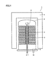
- Fig. 1 is a schematic cross-sectional view representing a CVD device used in a CVD step of the present invention.
- a surface coated member of the present invention has a configuration including a base member and a hard coating formed on a surface thereof.
- a coating coats an entire surface of the base member.
- a part of the base member is not coated with this coating, or a configuration of the coating is partially different, it does not depart from the scope of the present invention.
- Examples of such a surface coated member of the present invention include a cutting tool, a wear resistant tool, a mold component, an automobile part, and the like.
- the surface coated member can be suitably used as a cutting tool such as a drill, an end mill, a cutting edge replaceable-type cutting tip for a drill, a cutting edge replaceable-type cutting tip for an end mill, a cutting edge replaceable-type cutting tip for milling, a cutting edge replaceable-type cutting tip for turning, a metal saw, a gear cutting tool, a reamer, a tap, or the like.
- the base member used in the surface coated member of the present invention can be anything as long as it has been conventionally known as a base member of this kind.
- the base member is made of any of cemented carbide (for example, WC-base cemented carbide or a material containing WC and Co or carbonitride of Ti, Ta, Nb, or the like), a cermet (mainly composed of TiC, TiN, TiCN, or the like), a high-speed steel, a ceramic material (titanium carbide, silicon carbide, silicon nitride, aluminum nitride, aluminum oxide, and the like), a cubic crystal boron nitride sintered body, and a diamond sintered body.
- cemented carbide for example, WC-base cemented carbide or a material containing WC and Co or carbonitride of Ti, Ta, Nb, or the like
- a cermet mainly composed of TiC, TiN, TiCN, or the like
- a high-speed steel a ceramic
- WC-based cemented carbide or a cermet particularly, TiCN-base cermet. This is because these base members are particularly superior in balance between a hardness and a strength at a high temperature and have superior characteristics as a base member of a surface coated member for the above-described application.
- such a base member includes the one having a chip breaker and the one having no chip breaker, and a cutting-edge ridgeline portion has a shape including a sharp edge (a ridge at which a cutting face and a flank intersect), a honing (the one having an R shape given to a sharp edge), a negative land (the beveled one), and a combination of the honing and negative land.
- the hard coating of the present invention is constituted of one or more layers, and at least one among the layers is a layer including hard particles.
- the hard coating of the present invention has a thickness of 3 to 30 ⁇ m. When the thickness is less than 3 ⁇ m, there is a case where a wear resistance is not sufficient. When the thickness exceeds 30 ⁇ m, there is a case where peeling or breaking of the hard coating occurs frequently due to a great stress applied between the hard coating and the base member during the intermittent working.
- other layer may be included as long as at least one layer of hard particles is included.
- Other layers may include, for example, an Al 2 O 3 layer, a TiB 2 layer, a TiBN layer, an AlN layer (wurtzite type), a TiN layer, a TiCN layer, a TiBNO layer, a TiCNO layer, a TiAIN layer, a TiAlCN layer, a TiAlON layer, a TiAlONC layer, and the like.
- adhesion between the base member and the hard coating can be improved by including the TiN layer, TiC layer, TiCN layer, or TiBN layer as a base layer directly above the base member.
- the oxidation resistance of the hard coating can be improved by including the Al 2 O 3 layer.
- including an outermost layer made of the TiN layer, TiC layer, TiCN layer, TiBN layer, or the like can provide a distinctive characteristic on whether or not the cutting edge of the surface coated member is used. It should be noted that other layer may be typically formed to have a thickness of 0.1 to 10 ⁇ m.
- the hard coating of the present invention can have an indentation hardness greater than or equal to 3000 kgf/mm 2 . It should be noted that the indentation hardness can be measured by cutting a sample along a flat plane including a normal line with respect to the surface of the hard coating of the cutting tool and pressing an indentor at a load of 25 gmHv with respect to a hard particle layer in a direction perpendicular to the cut plane.
- the hard coating of the present invention is constituted of one or more layers, and at least one layer among the layers is a layer including hard particles (hereinafter, also referred to as "hard particle layer").
- the hard particle layer of the present invention suitably has a thickness greater than or equal to 1 ⁇ m and less than or equal to 20 ⁇ m, more preferably greater than or equal to 1 ⁇ m and less than or equal to 15 ⁇ m. When the thickness is less than 1 ⁇ m, there is a case where the wear resistance is insufficient. When the thickness exceeds 20 ⁇ m, there is a case where peeling or breaking of the hard coating frequently occurs due to a great stress applied to the hard coating and the base member during the intermittent working.
- the hard particle layer of the present invention partially includes the configuration other than the hard particles, for example, includes an amorphous phase or a wurtzite hard phase, it does not depart from the scope of the present invention as long as the effect of the present invention is exhibited.
- the hard particles of the present invention include a multilayer structure having the first unit layers and the second unit layers being layered alternately. It should be noted that, even when the hard particles of the present invention partially include the configuration other than the multilayer structure, for example, include an amorphous phase or a wurtzite hard phase, it does not depart from the scope of the present invention as long as the effect of the present invention is exhibited.
- the above-described first unit layer includes a first compound made of one or more kind of element selected from the group consisting of a periodic table group 4 element, a periodic table group 5 element, a periodic table group 6 element, and Al, and one or more kind of element selected from the group consisting of B, C, N, and O.
- the above-described second unit layer includes a second compound made of one or more kind of element selected from the group consisting of a periodic table group 4 element, a periodic table group 5 element, a periodic table group 6 element, and Al, and one ore more kind of element selected from the group consisting of B, C, N, and O. It goes without saying that the composition of the first compound and the composition of the second compound are different.
- the first compound and second compound made of one or more kind of element selected from the group consisting of a periodic table group 4 element, a periodic table group 5 element, a periodic table group 6 element, and Al, and one or more kind of element selected from the group consisting of B, C, N, and O respectively include TiC, TiN, TiCN, TiNO, TiCNO, TiB 2 , TiO 2 , TiBN, TiBNO, TiCBN, ZrC, ZrO 2 , HfC, HfN, TiAIN, TiAlCrN, TiZrN, TiCrN, AlCrN, CrN, VN, N, AlTiCrN, TiAlCN, ZrCN, ZrCNO, Al 2 O 3 , AlN, AICN, ZrN, TiAlC, NbC, NbN, NbCN, Mo 2 C, WC, W 2 C and the like. It should be noted that even when inevitable impurities are included in the first compound and second compound, it does not depart from
- the first unit layer and second unit layer of the present invention may have a configuration of a single composition or a configuration in which respective compositions are changed in the respective thickness directions.
- Such a configuration in which the composition is changed will be described for easy understanding by referring to the case where the composition at a midpoint in the thickness direction of the first unit layer is Al 0.9 Ti 0.1 N and where the composition at a midpoint in the thickness direction of the second unit layer is Al 0.1 Ti 0.9 N.
- the first unit layer contains Al 0.9 Ti 0.1 N at the midpoint, and the composition can be changed, from the midpoint to the side in contact with the adjacent second unit layer, into the composition having the atomic ratio of Al being gradually reduced from Al 0.9 Ti 0.1 N.
- the second unit layer contains Al 0.1 Ti 0.9 N at the midpoint, and the composition can be changed, from the midpoint to the side in contact with the adjacent first layer, into the composition having the atomic ratio of Ti being gradually reduced from Al 0.1 Ti 0.9 N. In other words, in this case, there is no clear boundary in the composition between the first unit layer and the second unit layer.
- the thickness in the layer cycle is preferably greater than or equal to 0.5 nm and less than or equal to 20 nm. It is difficult to set the layer cycle to be less than 0.5 nm in the sense of manufacturing technique. This is because, when the layer cycle exceeds 20 nm, the distortion between the unit layers is alleviated, and the superior characteristic as the hard phase is deteriorated.
- the thickness of the layer cycle represents a distance from one first unit layer to other adjacent first unit layer across the second unit layer adjacent to the one first unit layer (when an intermediate layer described later is included between the first unit layer and the second unit layer, the intermediate layer adjacent to the second unit layer is included). It should be noted that this distance is a distance connecting midpoints of each of the first unit layer and the other first unit layer in the thickness direction of each layer.
- the number of layers (the total number of layers) constituting this multilayer structure layer is not particularly limited but is preferably greater than or equal to 10 layers and less than or equal to 1000 layers. This is because, when the number of layers is less than 10 layers, the crystal grains in each layer become coarse and large, so that there is a case where the hardness of the hard particles is lowered, and it shows a tendency that each unit layer becomes thinner when the number exceeds 1000 layers and each of the layers is mixed.
- the multilayer structure and the particle diameter of the hard particles can be confirmed by means of a scanning electron microscope (SEM), a transmission electron microscope (TEM), a scanning electron microscope energy dispersive X-ray spectroscopy (EDX), an X-ray diffraction method, and the like. Since it is difficult to obtain hard particles having a particle diameter of less than 10 nm in the sense of manufacturing technique, and the particles having a particle diameter larger than 1000 nm causes falling and chipping, the particle diameter of hard particles is preferably greater than or equal to 10 nm and less than or equal to 1000 nm.
- the cause of improvement in the various characteristics such as the wear resistance and the welding resistance of the surface coated member by coating the base member with hard coating including a hard particle layer is unknown, but the following cause is presumed.
- at least one of the layers is constituted of a hard particle layer, so that the hard coating can have a region of a granular structure in its thickness direction. Accordingly, the toughness of the hard coating is improved.
- development of the crack into the base member can be suppressed effectively. Then, this effect is particularly fostered when each particle in the granular structure has a multilayer structure.
- the hard coating of the present invention can include an intermediate layer between the first unit layer and the second unit layer.
- the composition of this intermediate layer is changed continuously in its thickness direction from the composition of the first compound to the composition of the second compound from the side in contact with the first unit layer to the side in contact with the second unit layer.
- the intermediate layer can have the configuration having an atomic ratio of Ti reduced and an atomic ratio of Al increased from the side in contact with the first unit layer to the side in contact with the second unit layer.
- the intermediate layer can have the configuration having an tomic ratio of at least Ti reduced continuously from the side in contact with the first unit layer to the side in contact with the second unit layer.
- the thickness of the intermediate layer is not particularly limited.
- the thickness of the intermediate layer may be substantially equal to or smaller than the thickness of the first unit layer or second unit layer.
- the thickness of the intermediate layer may be exceedingly greater than the respective thickness of the first unit layer or second unit layer. In other words, the thickness of the first unit layer and second unit layer may be exceedingly smaller than the intermediate layer.
- the hard particle layer includes the intermediate layer between the first unit layer and the second unit layer, so that various characteristics such as the wear resistance and chipping resistance of the surface coated member further improves.
- the cause is not clear.
- the cause is related to the fact that a large distortion is accumulated in the hard particle layer since providing the intermediate layer changes the composition continuously between the first unit layer and the second unit layer.
- the cause is related to the fact that, since the layer becomes more thermally stable, the modification due to a thermal shock becomes more unlikely to occur, and the adhesion strength with the first unit layer and the second unit layer becomes higher due to the presence of the intermediate layer.
- the intermediate layer can be recognized as the first unit layer and/or second unit layer.
- the first compound is TiN
- the second compound is AlN
- the composition of the intermediate layer is Ti x Al y N
- the atomic ratio x of Ti decreases continuously from 1 to 0 and the atomic ratio y of Al continuously increases from 0 to 1 from the side in contact with the first unit layer to the side in contact with the second unit layer.
- the region having the atomic ratio x/y of Ti and Al is greater than or equal to 1 can be recognized as the first unit layer, and the region having the atomic ratio x/y of less than 1 can be considered as the second unit layer.
- the first unit layer and second unit layer have no clear boundary. It should be noted that, when the thickness of the first unit layer and/or second unit layer is exceedingly smaller than the intermediate layer, the region including the first compound in the first unit layer becomes a maximum point of the Ti concentration in the thickness direction of the layer cycle, and the region including the second compound in the second unit layer becomes a maximum point of the Al concentration in the thickness direction of the layer cycle.
- the first compound and second compound are Ti x Al y N respectively (however, the values of x and y are different respectively in the first compound and second compound), and more preferably, TiN and AlN.
- the first compound and second compound can be TiN having an fcc crystal structure (in the following, also referred to as "fcc-TiN") and AlN having an fcc crystal structure (in the following, also referred to as "fcc-AlN”), and the intermediate layer can change the composition in its thickness direction significantly.
- the hard particle layer of the present invention can have a grain boundary layer constituted of the first compound or second compound at the grain boundary between the hard particles, in other words, at the upper most surface of the hard particles.
- the composition of the grain boundary layer is TiN or AlN. Having this grain boundary layer further improves the various characteristics such as the wear resistance and chipping resistance of the surface coated member.
- the cause of it is not clear.
- the presence of the grain boundary layer improves the heat resistance of the hard particles, or the excessive particle growth of the hard particles is suppressed.
- the thickness thereof is preferably greater than or equal to 10 nm and less than or equal to 100 nm in view of the balance between the strength and toughness.
- the base member is coated with a hard coating including the hard particle layer, so that the various characteristics such as the wear resistance and welding resistance of the surface coated member improves.
- the present invention can provide a surface coated member having improved stability and a longer service life.
- a method for manufacturing a surface coated member according to the present invention is a method for manufacturing a surface coated member including a base member and a hard coating formed on a surface thereof and constituted of one or more layers.
- the method includes a CVD step of forming at least one layer among the layers by a CVD method.
- the CVD step includes an ejection step of ejecting a mixture gas, which contains two or more kinds of elements selected from the group consisting of a periodic table group 4 element, a periodic table group 5 element, a periodic table group 6 element, and Al, and one or more element selected from the group consisting of B, C, N, and O, to the surface of the base member, and a cooling step of cooling the base member after the ejection step.
- the method for manufacturing a surface coated member of the present invention can include other step as long as the above-described CVD step is performed.
- Other step may include, for example, a thermal treatment step such as annealing, a surface preparation step such as a surface grinding or a shot blasting, and a CVD step for providing another hard layer.
- a thermal treatment step such as annealing
- a surface preparation step such as a surface grinding or a shot blasting
- CVD step for providing another hard layer for providing another hard layer.
- the CVD step of the present invention is a step of forming at least one layer among the layers constituting the hard coating of the present invention by the CVD method.
- the CVD device shown in Fig. 1 can be used.
- a plurality of base member setting jigs 3 retaining base members 2 can be provided in a CVD device 1, and these are covered in a reactor vessel 4 made of heat-resistant alloy steel. Moreover, a temperature-adjusting device 5 is arranged around reactor vessel 4, and the temperature in reactor vessel 4 can be controlled by this temperature-adjusting device 5.
- a feed pipe 8 having two feed ports 6, 7 is arranged.
- Feed pipe 8 is arranged so as to pass through the region having base member setting jigs 3 arranged therein, and a plurality of through holes are formed in the portion near base member setting jigs 3.
- feed pipe 8 each gas introduced into the pipe from feed ports 6, 7 are not mixed in feed pipe 8 and are introduced into reactive vessel 4 through different through holes.
- Feed pipe 8 can rotate its axis as a center axis.
- an exhaust pipe 9 is arranged in CVD device 1, and exhaust gas can be discharged from an exhaust port 10 of exhaust pipe 9 to outside.
- the jigs in reactor vessel 4 are typically made of black lead.
- the CVD device shown in Fig. 1 is used to perform the ejection step and cooling step described below, so that the above-described hard particle layers can be formed.
- mixture gas containing two or more kinds of elements selected from the group consisting of a periodic table group 4 element, a periodic table group 5 element, a periodic table group 6 element, and Al, and one or more kind of element selected from the group consisting of B, C, N, and O is ejected to the surface of the base member.
- first gas containing two or more kinds of elements selected from the group consisting of a periodic table group 4 element, a periodic table group 5 element, a periodic table group 6 element, and Al is introduced from feed pipe 6 to feed pipe 8
- second gas containing one or more kind of element selected from the group consisting of B, C, N, and O are introduced from feed port 7 to feed pipe 8.
- first gas may be mixture gas, for example, first mixture gas of source gas containing the group 4 element, source gas containing the group 5 element, and carrier gas.
- the second gas may also be mixture gas, for example, second mixture gas of source gas containing B, source gas containing C, and carrier gas.
- first gas (or first mixture gas) and second gas (or second mixture gas) are ejected to reactor vessel 4 from different through holes.
- feed pipe 8 is rotated about its axis as indicated by the rotating arrow in the drawing. Therefore, the first gas (or first mixture gas) and second gas (or second mixture gas), as evenly mixture gas, are ejected to the surfaces of base members 2 set on base member setting jigs 3.
- chloride gas of these can be favorably used as the gas containing two or more kinds of elements selected from the group consisting of a periodic table group 4 element, a periodic group 5 element, a periodic table group 6 element, or Al.
- boron chloride gas such as BCl 3 gas can be used as gas containing B.
- Hydrocarbon gas such as CH 4 can be used as gas containing C.
- Gas containing nitrogen such as ammonia or N 2 can be used as gas containing N.
- H 2 O (vapor) can be used as gas containing O.
- the hydrocarbon gas is preferably unsaturated hydrocarbon.
- the temperature in reactor vessel 4 is preferably within the range of 700 to 900°C, and the pressure in reactor vessel 4 is preferably 0.1 to 13 kPa.
- H 2 gas, N 2 gas, and Ar gas can be used as carrier gas.
- the composition of the first unit layer, second unit layer, intermediate layer, grain boundary layer, and the like can be controlled by a mixing ratio of the source gas.
- the thickness of the hard particle layer can be controlled by adjusting a flow of the source gas and a film-forming time.
- the respective thicknesses and layer cycles of the first unit layer, the second unit layer, and the intermediate layer can be controlled by adjusting the film-forming time and the cooling rate.
- the number of layers of the hard particle layers can be controlled by adjusting the rotating speed of feed pipe 8 and the film-forming time.
- base members 2 are cooled after the ejection step.
- base members 2 set on base member setting jigs 3 can be cooled by temperature-adjusting device 5.
- base members 2 subjected to the thermal CVD treatment in a CVD furnace are cooled naturally by leaving.
- the cooling rate does not exceed 5°C/min, and the cooling rate becomes lower as the temperature of base members 2 is lowered.
- base members 2 are cooled at a rate which is at least higher than the natural cooling, in other words, cooled at a rate higher than or equal to 5°C/min. More preferably, base members 2 are cooled at a rate higher than or equal to 7°C/m.
- the above-described hard particle layers can be formed by the method described above in detail. Therefore, by forming the hard coating with use of the manufacturing method, a surface coated member having improved characteristics such as the wear resistance and welding resistance can be manufactured. Thus, the present invention can provide a surface coated member having improved stability and a longer service life.
- a base member A and a base member B described in the Table 1 below were prepared. Specifically, the material powders of the blend compositions described in Table 1 were evenly mixed and press-formed into a predetermined shape, and thereafter sintered at 1300 to 1500°C for one to two hours, so that base members made of cemented carbide having two kinds of shapes including CNMG120408NUX and SEET13T3AGSN-G were obtained. In other words, two different kinds of shapes were provided for each base member.
- CNMG120408NUX is a shape of a cutting edge replaceable-type cutting tip for turning
- SEET13T3AGSN-G is a shape of a cutting edge replaceable-type cutting tip for rotary cutting (milling).
- a hard coating was formed on the surface of each base member obtained as described above. Specifically, the CVD device shown in Fig. 1 was used, and the base members were set on base member setting jigs 3, and a thermal CVD method was conducted to form the hard coating on the base members.
- the conditions for forming each hard coating were as described in Table 2 and Table 3, and a flow of source gas, a mixing ratio of source gas, a film-forming time, and a cooling rate were adjusted so as to obtain each thickness described in Table 4. It should be noted that Table 2A shows forming conditions for hard particle layers, and Table 2B shows forming conditions for conventional hard layers, and Table 3 shows forming conditions for other layers.
- forming conditions a to g for the hard particle layers there were seven forming conditions a to g for the hard particle layers.
- x and y were conditions for Comparative Examples (Conventional Art).
- AlCl 3 gas was used as source gas containing Al
- TiCl 4 gas was used as source gas containing Ti
- these source gases were introduced from feed port 6 to feed pipe 8 as first mixture gas together with the carrier gas constituted of H 2 gas and N 2 gas.
- the source gas together with carrier gas constituted of N 2 gas were introduced from feed port 7 to feed pipe 8 as the second mixture gas.
- feed pipe 8 was rotated to allow the first mixture gas and second mixture gas to be ejected from the through holes of feed pipe 8 to thereby eject the mixture gas evenly containing the first mixture gas and second mixture gas toward the surfaces of the base members. After that, with temperature-adjusting device 5, the base member was cooled after the ejection step.
- the first mixture gas was obtained by mixing AlCl 3 gas of 0.065 mol/min, TiCl 4 gas of 0.025 mol/min, and H 2 gas and N 2 gas of 2.9 mol/min and 1.0 mol/min, and the first mixture gas was introduced from feed pipe 6 into reactor vessel 4.
- the atomic ratio of Al/Ti in the first mixture gas was 2.6.
- the second mixture gas was obtained by mixing NH 3 gas of 0.09 mol/min and N 2 gas of 0.9 mol/min, and the second mixture gas was introduced from feed pipe 7 into reactor vessel 4. Reactor vessel 4 at this time was retained in the condition with the pressure of 1.3 kPa and the temperature of 800°C.
- reactor vessel 4 was cooled at a cooling rate of 10°C/min until the temperature of the base member after the heat ejection step reached 200°C.
- the forming condition a provides "TiN (2 nm)/AlN (6nm)." This indicates that the thickness of the TiN layer as the first unit layer was 2 nm, and the thickness of the AlN layer as the second unit layer was 6 nm, and the layers were layered alternately.
- the "layer cycle” indicates a distance from a midpoint in the thickness direction of TiN layer to a midpoint in the thickness direction of an adjacent TiN layer through one AlN layer, in other words, a sum of the thickness of one TiN layer and the thickness of one AlN layer. It should be noted that the thickness of the hard particle layer was controlled by the film-forming time, and the layer cycle of TiN and AlN in the hard particle layer was controlled by the cooling rate of feed pipe 8.
- each layer other than the hard particle layers described in Table 3 were also formed in a similar manner except for that all of the gases such as source gas and carrier gas were introduced from feed port 6 and that the base member was cooled by the natural cooling after the thermal CVD treatment.
- the "Remainder” in Table 3 indicates that H 2 takes up the remainder of the source gas (reaction gas).
- Total Gas Amount indicates a total amount of flow introduced into the CVD furnace per unit time with gas in the reference condition (0°C, 1 atmospheric pressure) as ideal gas.
- the hard coating was formed with use of the PVD method disclosed in PTD 1, and the hard coating was formed with use of the CVD method disclosed in PTD 2 in the forming condition y.
- a layer (AlN/TiN layer) of a layered structure in which the TiN layer having a thickness of 4 nm and the AlN layer having a thickness of 4 nm were alternately layered was formed.
- a layer constituted mainly of the composition of Ti 0.1 Al 0.9 N (Ti 0.1 Al 0.9 N layer) was formed.
- a hard coating was formed on the base member in accordance with the above-described conditions of Table 2 and Table 3 to produce a cutting tool as surface coated members of Examples 1 to 15 and Comparative Examples 1 to 6 shown in following Table 4.
- the cutting tool of Example 13 employs base member B described in Table 1 as a base member.
- a TiN layer (base layer) having a thickness of 1.0 ⁇ m was formed as a base layer on the surface of base member B in the condition of Table 3.
- a TiCN layer having a thickness of 3.0 ⁇ m was formed on the TiN layer (base layer) in the condition of Table 3.
- a hard particle layer having a thickness of 5.0 ⁇ m was formed on the TiCN layer in the forming condition f of Table 2.
- a TiN layer (outermost layer) having a thickness of 0.5 ⁇ m was formed on the hard particle layer in the condition of Table 3. Accordingly, a hard coating having a total thickness of 9.0 ⁇ m was formed on the base member.
- the blank (hyphen) in Table 4 indicates that the corresponding layer is not formed.
- the base layer and the layer including a multilayer structure there is a layer which has the same composition but different thickness.
- the hard particle layer of Example 1 is a layer having a thickness of 5 ⁇ m formed by the forming condition a
- the hard particle layer of Example 6 is a layer having a thickness of 8 ⁇ m formed in forming condition a.
- the difference in the thicknesses of these layers was controlled by adjusting a forming time of a layer, in other words, a total time of ejecting the first gas and second gas alternately onto the surface of the base member.
- Example 1 A TiN (0.5)-TiCN (2.5) a (5.0) - 8.0
- Example 2 A TiN (0.5)-TiCN (2.5) b (3.0) - 6.0
- Example 3 A TiN (0.5)-TiCN (2.5) d (7.5) - 10.5
- Example 4 A TiN (0.5)-TiCN (2.5) f (12.0) - 15.0
- Example 5 A TiN (1.5) c (10.0) - 11.5
- Example 6 A TiN (1.5) a (8.0) - 9.5
- Example 7 A TiN (1.5) g (3.7) - 5.2
- Example 8 A TiN (1.5) e (15.0) - 16.5
- Example 9 A TiN (0.5)-TiCN (5.0) d (6.0) - 11.5
- Example 10 B TiN (1.0) a (5.0) TiN (1.0)
- each hard particle had a layered structure in which the fcc-TiN and fcc-AlN are alternately layered. Further, a layer made of fine fcc-TiN was present in the grain boundary of each hard particles. On the other hand, in each layer formed in each condition shown in Table 2B, the granular structure was not observed.
- the layer constituted of fcc-TiN is changed in its composition from TiN to AlN continuously as it came closer to the adjacent layer constituted of fcc-AlN, and the layer constituted of fcc-AlN was continuosly changed in its composition from AlN to TiN as it came closer to the adjacent layer constituted of fcc-TiN.
- the region having the highest atomic ratio in Ti can be considered as the first unit layer
- the region having the highest atomic ratio in Al can be considered as the second unit layer
- the region therebetween having its composition changed can be considered as the intermediate layer.
- the cutting tools of the Examples according to the present invention were, as compared to the cutting tools of Comparative Examples, superior in both the wear resistance and welding resistance, and had improved stability and a longer service life.
- the "Normal Wear” indicates a damage form constituted of only wear without occurrence of chipping or loss (having a smooth worn surface), and the “Fracture” indicates a large loss occurred in the cutting edge.
- the cutting tools of the Examples according to the present invention were, as compared to the cutting tools of Comparative Examples, superior in both the wear resistance and welding resistance, and had improved stability and a longer service life.
- the "Normal Wear” indicates a damage form constituted of only wear without occurrence of chipping or loss (having a smooth worn surface)
- the "Fracture” indicates a large loss occurred in the cutting edge
- the "Front Boundary Fine Chipping” indicates fine chipping occurred in the cutting edge part forming the machined surface.
- the cutting tools of the Examples according to the present invention were, as compared to the cutting tools having hard coating formed by the conventional CVD method, superior in the fatigue resistant toughness, and therefore were had improved stability and a longer service life.
- the path number is obtained by repeatedly performing the rotational cutting with use of a cutter having one cutting tool (a cutting edge replaceable-type cutting tip) from one end to the other end of one side surface (the surface of 300 mm x 80 mm) of the following work material (shape: a block-like shape of 300 mm x 100 mm x 80 mm) and obtaining the frequency of repetition (the path number with a value after the decimal point indicates that the above-described condition is obtained on the way from one end to the other end).
- the cutting distance indicates a total distance of the work material cut before reaching the above-described condition and corresponds to a product of the path number and the die length (300 mm) of the above-described side surface.
- the cutting tools of the example according to the present invention were, as compared to the cutting tools of the Comparative Examples, superior in the wear resistance, and therefore had improved stability and a longer service life.
- the "Normal Wear” indicates a damage form constituted only of wear without chipping or loss (having a smooth worn surface).
- the cutting tools of the Examples according to the present invention were, as compared to the cutting tools of the Comparative Examples, were superior in both the wear resistance and shock resistance, and had improved stability and a longer service life.
- the "Normal Wear” indicates a damage form constituted of only wear without occurrence of chipping or loss
- the "chipping” indicates a small loss occurred in the cutting edge part.
Abstract
Description
- The present invention relates to a surface coated member including a base member and a hard coating formed on a surface thereof, and a method for manufacturing the same.
- As a recent technical trend, producing a thinner and shorter surface coated member for a cutting tool or the like is on the main stream for the purpose of reducing a load on a global environment and efficiently utilizing a resource. Accordingly, providing a metal material having a higher strength and higher hardness used for a surface coated member is proceeding to secure a service life of a surface coated member and maintain its reliability. On the other hand, at metal working sites, it has been strongly requested to achieve improved accuracy of a worked part and reduced working cost to compete with newly emerging countries. Further, with the improvement in the performance of machining tools, the expectation for further high-speed working with a surface coated member is increasing. In the high-speed working, since a cutting edge of a surface coated member is exposed to a high-temperature and high-pressure environment, a surface coated member capable of having a longer service life even under a harsh environment will be requested in the future.
- For example, Japanese Patent Laying-Open No.
7-205362 group - Moreover, for example, Japanese National Patent Publication No.
2008-545063 -
- PTD 1: Japanese Patent Laying-Open No.
7-205362 - PTD 2: Japanese National Patent Publication No.
2008-545063 - However, as to PTD 1, there is a case where the hard coating formed by the PVD method contains impurities such as metals of Ti, Al, and alloy of those. Such impurities are referred to as droplets, which inhibit formation of the hard coating and causes falling of the hard coating during metal working. Moreover, from the part where the hard coating has fallen as a starting point, chipping, fracture, and the like of the hard coating is likely to occur. Consequently, it becomes difficult to obtain a longer service life of a surface coated member, and there is a case where the work quality and surface roughness of the work material are deteriorated.
- Moreover, as to
PTD 2, although the Ti1-xAlxN coating has a stoichiometric coefficient of 0.75<x≤0.93, generally, there is a tendency to cause a large distortion in a crystal structure when x is greater than 0.7 in this composition. It is well known that a Ti1-xAlxN crystal of a cubic crystal NaCl structure is modified into a hexagonal crystal wurzite structure to mitigate the distortion. Particularly, there is a tendency that this modification is accelerated at a high temperature. - During the metal working, a cutting tool and a work material repeat contact and release, and a load is applied to a surface of a cutting edge of the surface coated member in the cycles of heating and cooling. Therefore, a great thermal load is applied all the time to the surface coated member during the metal working, and a thermal fatigue occurs. This thermal fatigue accelerates the above-described modification. Further, along with the repeated cutting, the hard coating which has once modified is likely to cause chipping and fracture. Therefore, also in the technique disclosed in
PTD 2, there is a limit on a longer service life of a surface coated member in a high-speed working. - The present invention was made in view of the circumstance described above, and its object is to provide improved stability and a longer service life to a surface coated member and to provide a method for manufacturing the same.
- The present invention concerns a surface coated member including a base member and a hard coating formed on a surface thereof. The hard coating is constituted of one or more layers. At least one layer among the above-described layers is a layer including hard particles. The hard particles include a multilayer structure having first unit layers and second unit layers being layered alternately. The first unit layer includes a first compound. The first compound is made of one or more kind of element selected from the group consisting of a
periodic table group 4 element, aperiodic table group 5 element, aperiodic table group 6 element, and Al, and one or more kind of element selected from the group consisting of B, C, N, and O. The second unit layer includes a second compound. The second compound is made of one or more kind of element selected from the group consisting of aperiodic table group 4 element,group 5 element,group 6 element, and Al, and at least one element selected from the group consisting of B, C, N, and O. - Preferably, the above-described surface coated member includes an intermediate layer between the first unit layer and the second unit layer, and a composition of the intermediate layer is changed continuously in its thickness direction from a composition of the first compound to a composition of the second compound.
- Preferably, in the above-described surface coated member, the layer including hard particles includes a grain boundary layer in a grain boundary of the hard particles, said grain boundary layer including the first compound or the second compound.
- Moreover, the present invention concerns a method for manufacturing a surface coated member including a base member and a hard coating. The hard coating is formed on a surface of the base member and constituted of one or more layers. The method includes a CVD step of forming at least one layer among the above-described layers by a CVD method. The CVD step includes an ejection step of ejecting a mixture gas, containing two or more kinds of elements selected from the group consisting of a
periodic table group 4 element, aperiodic table group 5 element, aperiodic table group 6 element, and Al, and one or more kind of element selected from the group consisting of B, C, N, and O, to the surface of the base member, and a cooling step of cooling the base member after the ejection step. - Preferably, in the above-described manufacturing method, the base member is cooled at a rate greater than or equal to 7°C/min in the cooling step.
- According to the surface coated member of the present invention, the various characteristics such as a wear resistance and a welding resistance are improved. Therefore, it exhibits a superior effect of having improved stability and a longer service life. Moreover, according to the method for manufacturing a surface coated member of the present invention, various characteristics such as a wear resistance and a welding resistance are improved, so that a surface coated member having improved stability and a longer service life can be manufactured.
-
Fig. 1 is a schematic cross-sectional view representing a CVD device used in a CVD step of the present invention. - Hereinafter, the present invention will be described in detail.
- A surface coated member of the present invention has a configuration including a base member and a hard coating formed on a surface thereof. Preferably, such a coating coats an entire surface of the base member. However, even when a part of the base member is not coated with this coating, or a configuration of the coating is partially different, it does not depart from the scope of the present invention.
- Examples of such a surface coated member of the present invention include a cutting tool, a wear resistant tool, a mold component, an automobile part, and the like. Among those, the surface coated member can be suitably used as a cutting tool such as a drill, an end mill, a cutting edge replaceable-type cutting tip for a drill, a cutting edge replaceable-type cutting tip for an end mill, a cutting edge replaceable-type cutting tip for milling, a cutting edge replaceable-type cutting tip for turning, a metal saw, a gear cutting tool, a reamer, a tap, or the like.
- The base member used in the surface coated member of the present invention can be anything as long as it has been conventionally known as a base member of this kind. For example, it is preferable that the base member is made of any of cemented carbide (for example, WC-base cemented carbide or a material containing WC and Co or carbonitride of Ti, Ta, Nb, or the like), a cermet (mainly composed of TiC, TiN, TiCN, or the like), a high-speed steel, a ceramic material (titanium carbide, silicon carbide, silicon nitride, aluminum nitride, aluminum oxide, and the like), a cubic crystal boron nitride sintered body, and a diamond sintered body.
- Among those various kinds of base members, it is particularly preferable to select WC-based cemented carbide or a cermet (particularly, TiCN-base cermet). This is because these base members are particularly superior in balance between a hardness and a strength at a high temperature and have superior characteristics as a base member of a surface coated member for the above-described application.
- It should be noted that, when the surface coated member is a cutting edge replaceable-type cutting tip or the like, such a base member includes the one having a chip breaker and the one having no chip breaker, and a cutting-edge ridgeline portion has a shape including a sharp edge (a ridge at which a cutting face and a flank intersect), a honing (the one having an R shape given to a sharp edge), a negative land (the beveled one), and a combination of the honing and negative land.
- The hard coating of the present invention is constituted of one or more layers, and at least one among the layers is a layer including hard particles. Preferably, the hard coating of the present invention has a thickness of 3 to 30 µm. When the thickness is less than 3 µm, there is a case where a wear resistance is not sufficient. When the thickness exceeds 30 µm, there is a case where peeling or breaking of the hard coating occurs frequently due to a great stress applied between the hard coating and the base member during the intermittent working.
- In the hard coating of the present invention, other layer may be included as long as at least one layer of hard particles is included. Other layers may include, for example, an Al2O3 layer, a TiB2 layer, a TiBN layer, an AlN layer (wurtzite type), a TiN layer, a TiCN layer, a TiBNO layer, a TiCNO layer, a TiAIN layer, a TiAlCN layer, a TiAlON layer, a TiAlONC layer, and the like.
- For example, adhesion between the base member and the hard coating can be improved by including the TiN layer, TiC layer, TiCN layer, or TiBN layer as a base layer directly above the base member. Moreover, the oxidation resistance of the hard coating can be improved by including the Al2O3 layer. Moreover, including an outermost layer made of the TiN layer, TiC layer, TiCN layer, TiBN layer, or the like can provide a distinctive characteristic on whether or not the cutting edge of the surface coated member is used. It should be noted that other layer may be typically formed to have a thickness of 0.1 to 10 µm.
- It should be noted that, in the present invention, when the composition of each layer constituting the hard coating is expressed by the chemical formula such as "TiN" and "TiCN," the chemical formula not particularly specifying an atomic ratio does not indicate that the atomic ratio of each element is only "1" but includes all of the conventionally known atomic ratio.
- Moreover, the hard coating of the present invention can have an indentation hardness greater than or equal to 3000 kgf/mm2. It should be noted that the indentation hardness can be measured by cutting a sample along a flat plane including a normal line with respect to the surface of the hard coating of the cutting tool and pressing an indentor at a load of 25 gmHv with respect to a hard particle layer in a direction perpendicular to the cut plane.
- The hard coating of the present invention is constituted of one or more layers, and at least one layer among the layers is a layer including hard particles (hereinafter, also referred to as "hard particle layer"). The hard particle layer of the present invention suitably has a thickness greater than or equal to 1 µm and less than or equal to 20 µm, more preferably greater than or equal to 1 µm and less than or equal to 15 µm. When the thickness is less than 1 µm, there is a case where the wear resistance is insufficient. When the thickness exceeds 20 µm, there is a case where peeling or breaking of the hard coating frequently occurs due to a great stress applied to the hard coating and the base member during the intermittent working. It should be noted that, even when the hard particle layer of the present invention partially includes the configuration other than the hard particles, for example, includes an amorphous phase or a wurtzite hard phase, it does not depart from the scope of the present invention as long as the effect of the present invention is exhibited.
- The hard particles of the present invention include a multilayer structure having the first unit layers and the second unit layers being layered alternately. It should be noted that, even when the hard particles of the present invention partially include the configuration other than the multilayer structure, for example, include an amorphous phase or a wurtzite hard phase, it does not depart from the scope of the present invention as long as the effect of the present invention is exhibited.
- The above-described first unit layer includes a first compound made of one or more kind of element selected from the group consisting of a
periodic table group 4 element, aperiodic table group 5 element, aperiodic table group 6 element, and Al, and one or more kind of element selected from the group consisting of B, C, N, and O. The above-described second unit layer includes a second compound made of one or more kind of element selected from the group consisting of aperiodic table group 4 element, aperiodic table group 5 element, aperiodic table group 6 element, and Al, and one ore more kind of element selected from the group consisting of B, C, N, and O. It goes without saying that the composition of the first compound and the composition of the second compound are different. - The first compound and second compound made of one or more kind of element selected from the group consisting of a
periodic table group 4 element, aperiodic table group 5 element, aperiodic table group 6 element, and Al, and one or more kind of element selected from the group consisting of B, C, N, and O respectively include TiC, TiN, TiCN, TiNO, TiCNO, TiB2, TiO2, TiBN, TiBNO, TiCBN, ZrC, ZrO2, HfC, HfN, TiAIN, TiAlCrN, TiZrN, TiCrN, AlCrN, CrN, VN, N, AlTiCrN, TiAlCN, ZrCN, ZrCNO, Al2O3, AlN, AICN, ZrN, TiAlC, NbC, NbN, NbCN, Mo2C, WC, W2C and the like. It should be noted that even when inevitable impurities are included in the first compound and second compound, it does not depart from the scope of the present invention. - The first unit layer and second unit layer of the present invention may have a configuration of a single composition or a configuration in which respective compositions are changed in the respective thickness directions. Such a configuration in which the composition is changed will be described for easy understanding by referring to the case where the composition at a midpoint in the thickness direction of the first unit layer is Al0.9Ti0.1N and where the composition at a midpoint in the thickness direction of the second unit layer is Al0.1Ti0.9N.
- In the above-described case, the first unit layer, as to its composition in the thickness direction, contains Al0.9Ti0.1N at the midpoint, and the composition can be changed, from the midpoint to the side in contact with the adjacent second unit layer, into the composition having the atomic ratio of Al being gradually reduced from Al0.9Ti0.1N. Moreover, the second unit layer, as to its composition in the thickness direction, contains Al0.1Ti0.9N at the midpoint, and the composition can be changed, from the midpoint to the side in contact with the adjacent first layer, into the composition having the atomic ratio of Ti being gradually reduced from Al0.1Ti0.9N. In other words, in this case, there is no clear boundary in the composition between the first unit layer and the second unit layer.
- Moreover, in the above-described multilayer structure, the thickness in the layer cycle is preferably greater than or equal to 0.5 nm and less than or equal to 20 nm. It is difficult to set the layer cycle to be less than 0.5 nm in the sense of manufacturing technique. This is because, when the layer cycle exceeds 20 nm, the distortion between the unit layers is alleviated, and the superior characteristic as the hard phase is deteriorated. Herein, the thickness of the layer cycle represents a distance from one first unit layer to other adjacent first unit layer across the second unit layer adjacent to the one first unit layer (when an intermediate layer described later is included between the first unit layer and the second unit layer, the intermediate layer adjacent to the second unit layer is included). It should be noted that this distance is a distance connecting midpoints of each of the first unit layer and the other first unit layer in the thickness direction of each layer.
- The number of layers (the total number of layers) constituting this multilayer structure layer is not particularly limited but is preferably greater than or equal to 10 layers and less than or equal to 1000 layers. This is because, when the number of layers is less than 10 layers, the crystal grains in each layer become coarse and large, so that there is a case where the hardness of the hard particles is lowered, and it shows a tendency that each unit layer becomes thinner when the number exceeds 1000 layers and each of the layers is mixed.
- It should be noted that the multilayer structure and the particle diameter of the hard particles can be confirmed by means of a scanning electron microscope (SEM), a transmission electron microscope (TEM), a scanning electron microscope energy dispersive X-ray spectroscopy (EDX), an X-ray diffraction method, and the like. Since it is difficult to obtain hard particles having a particle diameter of less than 10 nm in the sense of manufacturing technique, and the particles having a particle diameter larger than 1000 nm causes falling and chipping, the particle diameter of hard particles is preferably greater than or equal to 10 nm and less than or equal to 1000 nm.
- In the present invention, the cause of improvement in the various characteristics such as the wear resistance and the welding resistance of the surface coated member by coating the base member with hard coating including a hard particle layer is unknown, but the following cause is presumed. In other words, among the plurality of layers constituting the hard coating, at least one of the layers is constituted of a hard particle layer, so that the hard coating can have a region of a granular structure in its thickness direction. Accordingly, the toughness of the hard coating is improved. Moreover, even when a crack occurs on the surface of the hard coating, development of the crack into the base member can be suppressed effectively. Then, this effect is particularly fostered when each particle in the granular structure has a multilayer structure.
- The hard coating of the present invention can include an intermediate layer between the first unit layer and the second unit layer. The composition of this intermediate layer is changed continuously in its thickness direction from the composition of the first compound to the composition of the second compound from the side in contact with the first unit layer to the side in contact with the second unit layer. For example, in the case where the composition of the first compound is TiN and where the composition of the second compound is AlN, the intermediate layer can have the configuration having an atomic ratio of Ti reduced and an atomic ratio of Al increased from the side in contact with the first unit layer to the side in contact with the second unit layer. Moreover, for example, in the case where the first compound is TiAIN and where the second compound is AlN, the intermediate layer can have the configuration having an tomic ratio of at least Ti reduced continuously from the side in contact with the first unit layer to the side in contact with the second unit layer.
- Moreover, the thickness of the intermediate layer is not particularly limited. For example, the thickness of the intermediate layer may be substantially equal to or smaller than the thickness of the first unit layer or second unit layer. Moreover, the thickness of the intermediate layer may be exceedingly greater than the respective thickness of the first unit layer or second unit layer. In other words, the thickness of the first unit layer and second unit layer may be exceedingly smaller than the intermediate layer.
- In the present invention, the hard particle layer includes the intermediate layer between the first unit layer and the second unit layer, so that various characteristics such as the wear resistance and chipping resistance of the surface coated member further improves. However, the cause is not clear. For example, it is considered that the cause is related to the fact that a large distortion is accumulated in the hard particle layer since providing the intermediate layer changes the composition continuously between the first unit layer and the second unit layer. Moreover, it is considered that the cause is related to the fact that, since the layer becomes more thermally stable, the modification due to a thermal shock becomes more unlikely to occur, and the adhesion strength with the first unit layer and the second unit layer becomes higher due to the presence of the intermediate layer.
- Moreover, the intermediate layer can be recognized as the first unit layer and/or second unit layer. For example, the case is assumed where the first compound is TiN, and the second compound is AlN, and the composition of the intermediate layer is TixAlyN, and the atomic ratio x of Ti decreases continuously from 1 to 0 and the atomic ratio y of Al continuously increases from 0 to 1 from the side in contact with the first unit layer to the side in contact with the second unit layer. In this case, for example, in the intermediate layer, the region having the atomic ratio x/y of Ti and Al is greater than or equal to 1 can be recognized as the first unit layer, and the region having the atomic ratio x/y of less than 1 can be considered as the second unit layer. In this case, the first unit layer and second unit layer have no clear boundary. It should be noted that, when the thickness of the first unit layer and/or second unit layer is exceedingly smaller than the intermediate layer, the region including the first compound in the first unit layer becomes a maximum point of the Ti concentration in the thickness direction of the layer cycle, and the region including the second compound in the second unit layer becomes a maximum point of the Al concentration in the thickness direction of the layer cycle.
- Moreover, in the hard particle layer of the present invention, preferably, the first compound and second compound are TixAlyN respectively (however, the values of x and y are different respectively in the first compound and second compound), and more preferably, TiN and AlN. Although the cause of this is not clear, the following cause is presumed. In other words, in this case, the first compound and second compound can be TiN having an fcc crystal structure (in the following, also referred to as "fcc-TiN") and AlN having an fcc crystal structure (in the following, also referred to as "fcc-AlN"), and the intermediate layer can change the composition in its thickness direction significantly. In such a configuration, being different from the layer such as fcc-Ti0.1Al0.9N having an even composition, distortion caused by the difference in the thermal expansion coefficient is present in the layer. With the presence of this distortion, a shift from the fcc crystal structure to an hcp crystal structure caused by a thermal load becomes particularly unlikely to occur. Consequently, the various characteristics such as the wear resistance and welding resistance improve.
- The matter which should be focused is that, when the thickness of the layer cycle exceeds 100 nm, AlN of the mechanically stable hexagonal crystal wurtzite structure is precipitated, and the above-described superior characteristics are deteriorated.
- The hard particle layer of the present invention can have a grain boundary layer constituted of the first compound or second compound at the grain boundary between the hard particles, in other words, at the upper most surface of the hard particles. For example, in the case where the first compound and second compound are TiN and AlN respectively, the composition of the grain boundary layer is TiN or AlN. Having this grain boundary layer further improves the various characteristics such as the wear resistance and chipping resistance of the surface coated member. However, the cause of it is not clear. For example, it is surmised that the presence of the grain boundary layer improves the heat resistance of the hard particles, or the excessive particle growth of the hard particles is suppressed. It should be noted that, as to the grain boundary layer, the thickness thereof is preferably greater than or equal to 10 nm and less than or equal to 100 nm in view of the balance between the strength and toughness.
- As described above in detail, according to the surface coated member of the present invention, the base member is coated with a hard coating including the hard particle layer, so that the various characteristics such as the wear resistance and welding resistance of the surface coated member improves. Thus, the present invention can provide a surface coated member having improved stability and a longer service life.
- A method for manufacturing a surface coated member according to the present invention is a method for manufacturing a surface coated member including a base member and a hard coating formed on a surface thereof and constituted of one or more layers. The method includes a CVD step of forming at least one layer among the layers by a CVD method. The CVD step includes an ejection step of ejecting a mixture gas, which contains two or more kinds of elements selected from the group consisting of a
periodic table group 4 element, aperiodic table group 5 element, aperiodic table group 6 element, and Al, and one or more element selected from the group consisting of B, C, N, and O, to the surface of the base member, and a cooling step of cooling the base member after the ejection step. It should be noted that, the method for manufacturing a surface coated member of the present invention can include other step as long as the above-described CVD step is performed. Other step may include, for example, a thermal treatment step such as annealing, a surface preparation step such as a surface grinding or a shot blasting, and a CVD step for providing another hard layer. In the following, each step of the present invention will be described in detail. - The CVD step of the present invention is a step of forming at least one layer among the layers constituting the hard coating of the present invention by the CVD method. In this CVD step, the CVD device shown in
Fig. 1 can be used. - Referring to
Fig. 1 , a plurality of basemember setting jigs 3retaining base members 2 can be provided in a CVD device 1, and these are covered in areactor vessel 4 made of heat-resistant alloy steel. Moreover, a temperature-adjustingdevice 5 is arranged aroundreactor vessel 4, and the temperature inreactor vessel 4 can be controlled by this temperature-adjustingdevice 5. - In CVD device 1, a
feed pipe 8 having twofeed ports Feed pipe 8 is arranged so as to pass through the region having basemember setting jigs 3 arranged therein, and a plurality of through holes are formed in the portion near base member setting jigs 3. Infeed pipe 8, each gas introduced into the pipe fromfeed ports feed pipe 8 and are introduced intoreactive vessel 4 through different through holes.Feed pipe 8 can rotate its axis as a center axis. Moreover, anexhaust pipe 9 is arranged in CVD device 1, and exhaust gas can be discharged from anexhaust port 10 ofexhaust pipe 9 to outside. It should be noted that, the jigs inreactor vessel 4 are typically made of black lead. - In this step, the CVD device shown in
Fig. 1 is used to perform the ejection step and cooling step described below, so that the above-described hard particle layers can be formed. - In this step, with use of the above-described CVD device, mixture gas containing two or more kinds of elements selected from the group consisting of a
periodic table group 4 element, aperiodic table group 5 element, aperiodic table group 6 element, and Al, and one or more kind of element selected from the group consisting of B, C, N, and O is ejected to the surface of the base member. - Specifically, for example, first gas containing two or more kinds of elements selected from the group consisting of a
periodic table group 4 element, aperiodic table group 5 element, aperiodic table group 6 element, and Al is introduced fromfeed pipe 6 to feedpipe 8, and second gas containing one or more kind of element selected from the group consisting of B, C, N, and O are introduced fromfeed port 7 to feedpipe 8. It should be noted that the first gas may be mixture gas, for example, first mixture gas of source gas containing thegroup 4 element, source gas containing thegroup 5 element, and carrier gas. The second gas may also be mixture gas, for example, second mixture gas of source gas containing B, source gas containing C, and carrier gas. - Since a plurality of through holes are formed in
feed pipe 8 on the upper side of the drawing, the introduced first gas (or first mixture gas) and second gas (or second mixture gas) are ejected toreactor vessel 4 from different through holes. At this time,feed pipe 8 is rotated about its axis as indicated by the rotating arrow in the drawing. Therefore, the first gas (or first mixture gas) and second gas (or second mixture gas), as evenly mixture gas, are ejected to the surfaces ofbase members 2 set on base member setting jigs 3. - As the gas containing two or more kinds of elements selected from the group consisting of a
periodic table group 4 element, aperiodic group 5 element, aperiodic table group 6 element, or Al, chloride gas of these can be favorably used. Moreover, boron chloride gas such as BCl3 gas can be used as gas containing B. Hydrocarbon gas such as CH4 can be used as gas containing C. Gas containing nitrogen such as ammonia or N2 can be used as gas containing N. H2O (vapor) can be used as gas containing O. It should be noted that the hydrocarbon gas is preferably unsaturated hydrocarbon. - Moreover, in this step, the temperature in
reactor vessel 4 is preferably within the range of 700 to 900°C, and the pressure inreactor vessel 4 is preferably 0.1 to 13 kPa. Moreover, H2 gas, N2 gas, and Ar gas can be used as carrier gas. It should be noted that the composition of the first unit layer, second unit layer, intermediate layer, grain boundary layer, and the like can be controlled by a mixing ratio of the source gas. The thickness of the hard particle layer can be controlled by adjusting a flow of the source gas and a film-forming time. The respective thicknesses and layer cycles of the first unit layer, the second unit layer, and the intermediate layer can be controlled by adjusting the film-forming time and the cooling rate. The number of layers of the hard particle layers can be controlled by adjusting the rotating speed offeed pipe 8 and the film-forming time. - Next, in this step,
base members 2 are cooled after the ejection step. For example,base members 2 set on basemember setting jigs 3 can be cooled by temperature-adjustingdevice 5. Typically,base members 2 subjected to the thermal CVD treatment in a CVD furnace are cooled naturally by leaving. In this case, the cooling rate does not exceed 5°C/min, and the cooling rate becomes lower as the temperature ofbase members 2 is lowered. On the other hand, according to the present invention,base members 2 are cooled at a rate which is at least higher than the natural cooling, in other words, cooled at a rate higher than or equal to 5°C/min. More preferably,base members 2 are cooled at a rate higher than or equal to 7°C/m. Moreover, in this cooling step, it is preferable to coolbase members 2 at least to the temperature lower than or equal to 300°C. Accordingly, more even hard particle layers can be formed. - The above-described hard particle layers can be formed by the method described above in detail. Therefore, by forming the hard coating with use of the manufacturing method, a surface coated member having improved characteristics such as the wear resistance and welding resistance can be manufactured. Thus, the present invention can provide a surface coated member having improved stability and a longer service life.
- In the following, examples of the present invention will be described in detail. However, the present invention is not limited to the examples.
- A base member A and a base member B described in the Table 1 below were prepared. Specifically, the material powders of the blend compositions described in Table 1 were evenly mixed and press-formed into a predetermined shape, and thereafter sintered at 1300 to 1500°C for one to two hours, so that base members made of cemented carbide having two kinds of shapes including CNMG120408NUX and SEET13T3AGSN-G were obtained. In other words, two different kinds of shapes were provided for each base member.
- Both of the two kinds of shapes described above are manufactured by Sumitomo Electric Hardmetal Division. CNMG120408NUX is a shape of a cutting edge replaceable-type cutting tip for turning, and SEET13T3AGSN-G is a shape of a cutting edge replaceable-type cutting tip for rotary cutting (milling).

- A hard coating was formed on the surface of each base member obtained as described above. Specifically, the CVD device shown in
Fig. 1 was used, and the base members were set on basemember setting jigs 3, and a thermal CVD method was conducted to form the hard coating on the base members. The conditions for forming each hard coating were as described in Table 2 and Table 3, and a flow of source gas, a mixing ratio of source gas, a film-forming time, and a cooling rate were adjusted so as to obtain each thickness described in Table 4. It should be noted that Table 2A shows forming conditions for hard particle layers, and Table 2B shows forming conditions for conventional hard layers, and Table 3 shows forming conditions for other layers. - As shown in Table 2A, there were seven forming conditions a to g for the hard particle layers. As shown in Fig. 2B, x and y were conditions for Comparative Examples (Conventional Art). In the forming conditions a to g, AlCl3 gas was used as source gas containing Al, and TiCl4 gas was used as source gas containing Ti, and these source gases were introduced from
feed port 6 to feedpipe 8 as first mixture gas together with the carrier gas constituted of H2 gas and N2 gas. Moreover, with use of NH3 gas as source gas containing N, the source gas together with carrier gas constituted of N2 gas were introduced fromfeed port 7 to feedpipe 8 as the second mixture gas. Then,feed pipe 8 was rotated to allow the first mixture gas and second mixture gas to be ejected from the through holes offeed pipe 8 to thereby eject the mixture gas evenly containing the first mixture gas and second mixture gas toward the surfaces of the base members. After that, with temperature-adjustingdevice 5, the base member was cooled after the ejection step. - Specifically, in the forming condition a for example, the first mixture gas was obtained by mixing AlCl3 gas of 0.065 mol/min, TiCl4 gas of 0.025 mol/min, and H2 gas and N2 gas of 2.9 mol/min and 1.0 mol/min, and the first mixture gas was introduced from
feed pipe 6 intoreactor vessel 4. Thus, the atomic ratio of Al/Ti in the first mixture gas was 2.6. Moreover, the second mixture gas was obtained by mixing NH3 gas of 0.09 mol/min and N2 gas of 0.9 mol/min, and the second mixture gas was introduced fromfeed pipe 7 intoreactor vessel 4.Reactor vessel 4 at this time was retained in the condition with the pressure of 1.3 kPa and the temperature of 800°C. Then, the first mixture gas and second mixture gas were ejected from the through holes offeed pipe 3 by the rotation offeed pipe 8, so that mixture gas constituted of evenly mixed first mixture gas and second mixture gas was ejected to the surface of the base member. After that,reactor vessel 4 was cooled at a cooling rate of 10°C/min until the temperature of the base member after the heat ejection step reached 200°C. - Moreover, referring to Table 2A, the forming condition a provides "TiN (2 nm)/AlN (6nm)." This indicates that the thickness of the TiN layer as the first unit layer was 2 nm, and the thickness of the AlN layer as the second unit layer was 6 nm, and the layers were layered alternately. The "layer cycle" indicates a distance from a midpoint in the thickness direction of TiN layer to a midpoint in the thickness direction of an adjacent TiN layer through one AlN layer, in other words, a sum of the thickness of one TiN layer and the thickness of one AlN layer. It should be noted that the thickness of the hard particle layer was controlled by the film-forming time, and the layer cycle of TiN and AlN in the hard particle layer was controlled by the cooling rate of
feed pipe 8. - Moreover, each layer other than the hard particle layers described in Table 3 were also formed in a similar manner except for that all of the gases such as source gas and carrier gas were introduced from
feed port 6 and that the base member was cooled by the natural cooling after the thermal CVD treatment. It should be noted that the "Remainder" in Table 3 indicates that H2 takes up the remainder of the source gas (reaction gas). Moreover, "Total Gas Amount" indicates a total amount of flow introduced into the CVD furnace per unit time with gas in the reference condition (0°C, 1 atmospheric pressure) as ideal gas. - In the forming condition x, the hard coating was formed with use of the PVD method disclosed in PTD 1, and the hard coating was formed with use of the CVD method disclosed in
PTD 2 in the forming condition y. It should be noted that, in the forming condition x, a layer (AlN/TiN layer) of a layered structure in which the TiN layer having a thickness of 4 nm and the AlN layer having a thickness of 4 nm were alternately layered was formed. In the forming condition y, a layer constituted mainly of the composition of Ti0.1Al0.9N (Ti0.1Al0.9N layer) was formed.

[Table 3] Configuration of Cover Film-Forming Conditions Reaction Atmosphere Composition Reaction Gas Composition (Volume%) Pressure (kPa) Temperature (°C) Total Gas Amount (L/min) TiN(Base Layer) TiCl4=2.0%, N2=39.7%, H2=Remainder 6.7 915 63.8 TiN(Outermost layer) TiCl4=0.5%, N2=41.2%, H2=Remainder 79.8 980 45.9 TiCN TiCl4=2.0%, CH3CN=0.7%, H2= Remainder 9 860 50.5 TiBNO TiCl4=36.7%, BCl3=0.1%, CO=1.6%, CO2=1.7%, N2=61.7%, H2=Remainer 6.7 980 80.3 TiCNO TiCl4=2.1%, CO=3.2%, CH4=2.8%, N2=23.7%, H2=Remainder 16.0 1030 70.5 Al2O3 AlCl3=1.6%, CO2=4.5%, H2S=0.2%, HCl=3.5%, H2=Remainder 6.7 1000 46.2 - A hard coating was formed on the base member in accordance with the above-described conditions of Table 2 and Table 3 to produce a cutting tool as surface coated members of Examples 1 to 15 and Comparative Examples 1 to 6 shown in following Table 4.
- For example, the cutting tool of Example 13 employs base member B described in Table 1 as a base member. A TiN layer (base layer) having a thickness of 1.0 µm was formed as a base layer on the surface of base member B in the condition of Table 3. A TiCN layer having a thickness of 3.0 µm was formed on the TiN layer (base layer) in the condition of Table 3. A hard particle layer having a thickness of 5.0 µm was formed on the TiCN layer in the forming condition f of Table 2. A TiN layer (outermost layer) having a thickness of 0.5 µm was formed on the hard particle layer in the condition of Table 3. Accordingly, a hard coating having a total thickness of 9.0 µm was formed on the base member. The blank (hyphen) in Table 4 indicates that the corresponding layer is not formed.
- It should be noted that, as to the base layer and the layer including a multilayer structure, there is a layer which has the same composition but different thickness. For example, although the hard particle layer of Example 1 is a layer having a thickness of 5 µm formed by the forming condition a, the hard particle layer of Example 6 is a layer having a thickness of 8 µm formed in forming condition a. The difference in the thicknesses of these layers was controlled by adjusting a forming time of a layer, in other words, a total time of ejecting the first gas and second gas alternately onto the surface of the base member.
[Table 4] Kind of Base Layer Configuration and Thickness of Each Layer Base Layer (µm) Hard Particle Layer (µm) Outermost Layer (µm) Total Layer Thickness (µm) Example 1 A TiN (0.5)-TiCN (2.5) a (5.0) - 8.0 Example 2 A TiN (0.5)-TiCN (2.5) b (3.0) - 6.0 Example 3 A TiN (0.5)-TiCN (2.5) d (7.5) - 10.5 Example 4 A TiN (0.5)-TiCN (2.5) f (12.0) - 15.0 Example 5 A TiN (1.5) c (10.0) - 11.5 Example 6 A TiN (1.5) a (8.0) - 9.5 Example 7 A TiN (1.5) g (3.7) - 5.2 Example 8 A TiN (1.5) e (15.0) - 16.5 Example 9 A TiN (0.5)-TiCN (5.0) d (6.0) - 11.5 Example 10 B TiN (1.0) a (5.0) TiN (1.0) 6.0 Example 11 B TiN (1.0) d (6.5) - 7.5 Example 12 B TiN (1.0) g (5.5) - 6.5 Example 13 B TiN (1.0)-TiCN (3.0) f (5.0) TiN (0.5) 9.0 Example 14 B TiN (1.0)-TiCN (3.0) a (4.0) - 8.0 Example 15 B TiN (1.0)-TiCN (3.0) b (2.5) TiBN (0.3)-Al2O3(1.0) 7.8 Comparative Example 1 A - x (10.0) - 10.0 Comparative Example 2 A TiN (0.5)-TiCN (2.5) x (5.0) - 8.0 Comparative Example 3 B TiN (1.0) x (5.0) TiN (1.0) 7.0 Comparative Example 4 A TiN (0.5)-TiCN (2.5) y (5.0) - 8.0 Comparative Example 5 A TiN (1.5) y (10.0) TiN (0.5) 11.5 Comparative Example 6 B TiN (1.0)-TiCN (3.0) y (5.0) - 9 - When the coated hard coating was observed with use of a transmission electron microscope and an X-ray diffraction method, a granular structure constituted of hard particles was observed in the hard particle layer formed in each condition shown in Table 2A. Moreover, each hard particle had a layered structure in which the fcc-TiN and fcc-AlN are alternately layered. Further, a layer made of fine fcc-TiN was present in the grain boundary of each hard particles. On the other hand, in each layer formed in each condition shown in Table 2B, the granular structure was not observed.
- It should be noted that, although the respective thicknesses of layers constituted of fcc-TiN and layers constituted of fcc-AlN are shown in Table 2A based on the above-described observation, this is based on that, in the microscope observation, in the region where the layer structure is observed, the region having a higher atomic ratio in Ti than Al is considered as TiN, and the region having a higher atomic ratio in Al than Ti is considered as AlN. In other words, the layer constituted of fcc-TiN is changed in its composition from TiN to AlN continuously as it came closer to the adjacent layer constituted of fcc-AlN, and the layer constituted of fcc-AlN was continuosly changed in its composition from AlN to TiN as it came closer to the adjacent layer constituted of fcc-TiN. In this case, in the thickness direction of the hard particle layer, the region having the highest atomic ratio in Ti can be considered as the first unit layer, and the region having the highest atomic ratio in Al can be considered as the second unit layer, and the region therebetween having its composition changed can be considered as the intermediate layer.
- With use of the cutting tool obtained as described above, the following five kinds of cutting experiments were conducted.
- As to the cutting tools of Examples and Comparative Examples described in the following Table 5 (the base member having a shape of CNMG120408NUX was used), the machining time to obtain the flank wear amount (Vb) of 0.20 mm under the following cutting condition was measured, and the final damage form of the cutting edge was observed. The result is shown in Table 5. It indicates that, as the machining time is longer, the wear resistance is superior. Moreover, it indicates that, as the final damage form is closer to the normal wear, the welding resistance is superior.
- Work Material: SUS316 round bar outer periphery cutting
Peripheral Speed: 200 m/min
Feed Rate: 0.15 mm/rev
Cutting Amount: 1.0 mm
Cutting Liquid: Present[Table 5] Cutting Time (min) Final Damage Form Example 1 17.0 Normal Wear Example 3 15.0 Normal Wear Example 7 19.0 Normal Wear Example 9 20.0 Normal Wear Comparative Example 1 7.0 Normal Wear Comparative Example 2 6.0 Fracture Comparative Example 4 13.0 Normal Wear - As is clear from Table 5, the cutting tools of the Examples according to the present invention were, as compared to the cutting tools of Comparative Examples, superior in both the wear resistance and welding resistance, and had improved stability and a longer service life. It should be noted that, in the final damage form of Table 5, the "Normal Wear" indicates a damage form constituted of only wear without occurrence of chipping or loss (having a smooth worn surface), and the "Fracture" indicates a large loss occurred in the cutting edge.
- As to the cutting tools of the Examples and Comparative Examples described in the following Table 6 (the base member having a shape of CNMG120408NUX is used), the machining time to obtain the flank wear amount (Vb) of 0.20 mm under the following cutting condition was measured, and the final damage form of the cutting edge was observed. The result is shown in Table 6. It indicates that, as the machining time is longer, the wear resistance is superior. Moreover, it indicates that, as the final damage form is closer to the normal wear, the welding resistance is superior.
- Work Material: FCD700 round bar outer periphery cutting
Peripheral Speed: 150 m/min
Feed Rate: 0.15 mm/rev
Cutting Amount: 1.0 mm
Cutting Liquid: Present[Table 6] Cutting Time (min) Final Damage Form Example 1 18.0 Normal Wear Example 4 23.0 Normal Wear Example 5 20.0 Normal Wear Example 8 17.0 Normal Wear Comparative Example 2 9.0 Fracture Comparative Example 4 13.0 Front Boundary Fine Chipping - As is clear from Table 6, the cutting tools of the Examples according to the present invention were, as compared to the cutting tools of Comparative Examples, superior in both the wear resistance and welding resistance, and had improved stability and a longer service life. It should be noted that, in the final damage form of Table 6, the "Normal Wear" indicates a damage form constituted of only wear without occurrence of chipping or loss (having a smooth worn surface), and the "Fracture" indicates a large loss occurred in the cutting edge, and the "Front Boundary Fine Chipping" indicates fine chipping occurred in the cutting edge part forming the machined surface.
- As to the cutting tools of Examples and Comparative Examples described in the following Table 7 (the base member having a shape of CNMG120408NUX was used), the machining time (minute) to occurrence of fracture or chipping in the tool cutting edge under the following cutting condition was measured. The result is shown in Table 7. It indicates that, as the machining time is longer, the fatigue resistant toughness is superior.
- Work Material: SCM435 groove material
Cutting Speed: 200 m/min
Feed Rate: 0.3 mm/s
Cutting Amount: 1.0 mm
Cutting Liquid: Present[Table 7] Cutting Time (min) Example 1 6.0 Example 2 7.0 Example 3 4.0 Example 5 4.0 Example 6 4.5 Comparative Example 2 5.0 Comparative Example 4 3.0 Comparative Example 5 1.0 - As is clear from Table 7, the cutting tools of the Examples according to the present invention were, as compared to the cutting tools having hard coating formed by the conventional CVD method, superior in the fatigue resistant toughness, and therefore were had improved stability and a longer service life.
- As to the cutting tools of the Examples and Comparative Examples described in the following Table 8 (the base member having the shape of ET13T3AGSN-G was used), the path number and cutting distance to obtain the cutting or flank wear amount (Vb) of 0.20 mm under the following cutting condition was measured, and the final damage form of the cutting edge was observed. The result is shown in Table 8. It indicates that, as the path number is larger (as the cutting distance is longer), the wear resistance is superior. Moreover, it indicates that, as the final damage form is closer to the normal wear, the shock resistance is superior.
- It should be noted that the path number is obtained by repeatedly performing the rotational cutting with use of a cutter having one cutting tool (a cutting edge replaceable-type cutting tip) from one end to the other end of one side surface (the surface of 300 mm x 80 mm) of the following work material (shape: a block-like shape of 300 mm x 100 mm x 80 mm) and obtaining the frequency of repetition (the path number with a value after the decimal point indicates that the above-described condition is obtained on the way from one end to the other end). The cutting distance indicates a total distance of the work material cut before reaching the above-described condition and corresponds to a product of the path number and the die length (300 mm) of the above-described side surface.
- Work Material: FC250 block material
Peripheral Speed: 300 m/min
Feed Rate: 0.3 mm/s
Cutting Amount: 2.0 mm
Cutting Liquid: Present
Cutter: WGC4160R (manufactured by Sumitomo Electric Hardmetal Division)[Table 8] Path Number Cutting Distance(m) Final Damage Form Example 10 12.6 3.8 Normal Wear Example 11 11.5 3.5 Normal Wear Example 13 14.0 4.2 Normal Wear Example 15 15.0 4.5 Normal Wear Comparative Example 3 6.0 1.8 Normal Wear Comparative Example 6 8.0 2.4 Normal Wear - As is clear from Table 8, the cutting tools of the example according to the present invention were, as compared to the cutting tools of the Comparative Examples, superior in the wear resistance, and therefore had improved stability and a longer service life. It should be noted that, in the final damage form of Table 8, the "Normal Wear" indicates a damage form constituted only of wear without chipping or loss (having a smooth worn surface).
- As to the cutting tools of the Examples and Comparative Examples described in the following Table 9 (the cutting tool having the shape of SEET13T3AGSN-G was used), the path number and cutting distance to obtain the cutting or flank wear amount (Vb) of 0.20 mm under the following cutting condition was measured, and the final damage form of the cutting edge was observed. The result is shown in Table 9. It indicates that, as the path number is larger (in other words, the cutting distance is longer), the wear resistance is superior. Moreover, it indicates that, as the final damage form is closer to the normal wear, the shock resistance is superior.
- Work Material: SUS304 block material
Peripheral Speed: 160 m/min
Feed Rate: 0.3 mm/s
Cutting Amount: 2.0 mm
Cutting Liquid: Absent
Cutter: WGC4160R (manufactured by Sumitomo Electric Hardmetal Division)[Table 9] Path Number Cutting Distance(m) Final Damage Form Example 10 7.0 2.1 Normal Wear Example 12 8.0 2.4 Normal Wear Example 13 10.0 3.0 Normal Wear Example 14 11.0 3.3 Normal Wear Comparative Example 3 2.5 0.8 Chipping Comparative Example 6 5.5 1.7 Chipping - As is clear from Table 9, the cutting tools of the Examples according to the present invention were, as compared to the cutting tools of the Comparative Examples, were superior in both the wear resistance and shock resistance, and had improved stability and a longer service life. It should be noted that, in the final damage form of Table 9, the "Normal Wear" indicates a damage form constituted of only wear without occurrence of chipping or loss, and the "chipping" indicates a small loss occurred in the cutting edge part.
- As described above, the embodiment and examples of the present invention were described. However, the appropriate combinations of each embodiment and example described above was expected from the original.
- It is to be understood that the embodiments and examples disclosed herein are only by way of example in all aspects, and not to be taken by way of limitation. The scope of the present invention is not limited by the description above, but rather by the terms of the appended claims, and is intended to include any modifications within the scope and meaning equivalent to the terms of the claims.
- 1 CVD device; 2 base member; 3 base member setting jig; 4 reactor vessel; 5 temperature-adjusting device; 6, 7 feed port; 8 feed pipe; 9 exhaust pipe; 10 exhaust port.
Claims (5)
- A surface coated member comprising a base member and a hard coating formed on a surface thereof,
said hard coating being constituted of one or more layers,
at least one layer among said layers being a layer including hard particles,
said hard particles including a multilayer structure having first unit layers and second unit layers being layered alternately,
said first unit layer including a first compound, said first compound being made of one or more kind of element selected from the group consisting of a periodic table group 4 element, a periodic table group 5 element, a periodic table group 6 element, and Al, and one or more kind of element selected from the group consisting of B, C, N, and O,
said second unit layer including a second compound, said second compound being made of one or more kind of element selected from the group consisting of a periodic table group 4 element, a periodic table group 5 element, a periodic table group 6 element, and Al, and one or more kind of element selected from the group consisting of B, C, N, and O. - The surface coated member according to claim 1, wherein
said surface coated member includes an intermediate layer between said first unit layer and said second unit layer, and
a composition of said intermediate layer is changed continuously in its thickness direction from a composition of said first compound to a composition of said second compound. - The surface coated member according to claim 1 or 2, wherein said layer including said hard particles includes a grain boundary layer in a grain boundary of said hard particles, said grain boundary including said first compound or said second compound.
- A method for manufacturing a surface coated member including a base member and a hard coating, said hard coating being formed on a surface of said base member and constituted of one or more layers, the method comprising:a CVD step of forming at least one layer among said layers by a CVD method,said CVD step including:an ejection step of ejecting a mixture gas, containing two or more kinds of elements selected from the group consisting of a periodic table group 4 element, a periodic table group 5 element, a periodic table group 6 element, and Al, and one or more kind of element selected from the group consisting of B, C, N, and O, to a surface of said base member; anda cooling step of cooling said base member after said ejection step.
- The method for manufacturing a surface coated member according to claim 4, wherein, said base member is cooled at a rate greater than or equal to 7°C/min in said cooling step.
Priority Applications (1)
| Application Number | Priority Date | Filing Date | Title |
|---|---|---|---|
| EP18153808.3A EP3336218B1 (en) | 2012-12-28 | 2013-11-11 | Surface coated member |
Applications Claiming Priority (2)
| Application Number | Priority Date | Filing Date | Title |
|---|---|---|---|
| JP2012287499A JP5618429B2 (en) | 2012-12-28 | 2012-12-28 | Surface covering member and manufacturing method thereof |
| PCT/JP2013/080395 WO2014103533A1 (en) | 2012-12-28 | 2013-11-11 | Surface coated member, and manufacturing method for same |
Related Child Applications (2)
| Application Number | Title | Priority Date | Filing Date |
|---|---|---|---|
| EP18153808.3A Division EP3336218B1 (en) | 2012-12-28 | 2013-11-11 | Surface coated member |
| EP18153808.3A Division-Into EP3336218B1 (en) | 2012-12-28 | 2013-11-11 | Surface coated member |
Publications (3)
| Publication Number | Publication Date |
|---|---|
| EP2940181A1 true EP2940181A1 (en) | 2015-11-04 |
| EP2940181A4 EP2940181A4 (en) | 2016-08-03 |
| EP2940181B1 EP2940181B1 (en) | 2018-03-14 |
Family
ID=51020632
Family Applications (2)
| Application Number | Title | Priority Date | Filing Date |
|---|---|---|---|
| EP18153808.3A Active EP3336218B1 (en) | 2012-12-28 | 2013-11-11 | Surface coated member |
| EP13869621.6A Active EP2940181B1 (en) | 2012-12-28 | 2013-11-11 | Surface coated member, and manufacturing method for same |
Family Applications Before (1)
| Application Number | Title | Priority Date | Filing Date |
|---|---|---|---|
| EP18153808.3A Active EP3336218B1 (en) | 2012-12-28 | 2013-11-11 | Surface coated member |
Country Status (6)
| Country | Link |
|---|---|
| US (2) | US20150345013A1 (en) |
| EP (2) | EP3336218B1 (en) |
| JP (1) | JP5618429B2 (en) |
| KR (2) | KR101843329B1 (en) |
| CN (2) | CN107761073B (en) |
| WO (1) | WO2014103533A1 (en) |
Cited By (2)
| Publication number | Priority date | Publication date | Assignee | Title |
|---|---|---|---|---|
| EP3357614A4 (en) * | 2016-01-13 | 2018-08-08 | Sumitomo Electric Hardmetal Corp. | Surface-coated cutting tool and method for producing same |
| EP3711883A4 (en) * | 2017-11-16 | 2021-08-25 | MOLDINO Tool Engineering, Ltd. | Coated cutting tool, and manufacturing method and chemical vapor deposition device for same |
Families Citing this family (26)
| Publication number | Priority date | Publication date | Assignee | Title |
|---|---|---|---|---|
| CN105899710B (en) * | 2014-01-10 | 2018-03-27 | 三菱综合材料株式会社 | Chemical evaporation plating device and chemical vapor deposition method |
| JP6511742B2 (en) * | 2014-07-17 | 2019-05-15 | 大日本印刷株式会社 | Authenticity judgment tool |
| JP6120229B2 (en) | 2015-01-14 | 2017-04-26 | 住友電工ハードメタル株式会社 | Hard coating, cutting tool, and manufacturing method of hard coating |
| AT516062B1 (en) * | 2015-01-15 | 2016-02-15 | Boehlerit Gmbh & Co Kg | Process for coating an article and coating made therewith |
| WO2017010426A1 (en) * | 2015-07-10 | 2017-01-19 | 三菱マテリアル株式会社 | Chemical vapor deposition device and chemical vapor deposition method |
| JP2017020111A (en) * | 2015-07-10 | 2017-01-26 | 三菱マテリアル株式会社 | Chemical vapor deposition apparatus and chemical vapor deposition method |
| EP3382058A4 (en) | 2015-11-25 | 2019-07-03 | Mitsubishi Hitachi Tool Engineering, Ltd. | Titanium aluminum nitride hard film, hard film coated tool, method for producing titanium aluminum nitride hard film, and method for producing hard film coated tool |
| JP6222675B2 (en) * | 2016-03-28 | 2017-11-01 | 住友電工ハードメタル株式会社 | Surface-coated cutting tool and method for manufacturing the same |
| JP6037255B1 (en) * | 2016-04-08 | 2016-12-07 | 住友電工ハードメタル株式会社 | Surface-coated cutting tool and manufacturing method thereof |
| JP6037256B1 (en) | 2016-04-14 | 2016-12-07 | 住友電工ハードメタル株式会社 | Surface-coated cutting tool and manufacturing method thereof |
| US11220760B2 (en) | 2016-04-14 | 2022-01-11 | Sumitomo Electric Hardmetal Corp. | Surface-coated cutting tool and method of producing the same |
| US11015242B2 (en) * | 2016-07-07 | 2021-05-25 | Moldino Tool Engineering, Ltd. | Hard coating, hard-coated tool, and their production methods |
| US11020804B2 (en) | 2017-02-28 | 2021-06-01 | Sumitomo Electric Hardmetal Corp. | Surface-coated cutting tool and method for manufacturing the same |
| EP3590638B1 (en) | 2017-02-28 | 2024-01-17 | Sumitomo Electric Hardmetal Corp. | Surface-coated cutting tool and method for manufacturing the same |
| US11123802B2 (en) | 2017-02-28 | 2021-09-21 | Sumitomo Electric Hardmetal Corp. | Surface-coated cutting tool and method for manufacturing the same |
| US11299807B2 (en) * | 2017-09-29 | 2022-04-12 | Mitsubishi Materials Corporation | Surface-coated cutting tool in which hard coating layer exhibits exceptional adhesion resistance and anomalous damage resistance |
| CN111902228B (en) * | 2018-03-22 | 2023-01-31 | 住友电工硬质合金株式会社 | Surface-coated cutting tool and method for manufacturing same |
| KR102350224B1 (en) * | 2018-03-22 | 2022-01-14 | 스미또모 덴꼬오 하드메탈 가부시끼가이샤 | Surface-coated cutting tool and manufacturing method thereof |
| KR102350221B1 (en) * | 2018-03-22 | 2022-01-14 | 스미또모 덴꼬오 하드메탈 가부시끼가이샤 | Surface-coated cutting tool and manufacturing method thereof |
| US10875101B2 (en) * | 2018-03-22 | 2020-12-29 | Sumitomo Electric Hardmetal Corp. | Surface-coated cutting tool and method for manufacturing same |
| US11274366B2 (en) * | 2018-03-22 | 2022-03-15 | Sumitomo Electric Hardmetal Corp. | Surface-coated cutting tool and method for manufacturing same |
| CN112996945B (en) * | 2018-07-10 | 2024-04-05 | 耐科思特生物识别集团股份公司 | Heat conduction and protective coating for electronic equipment |
| JP7165594B2 (en) * | 2019-02-07 | 2022-11-04 | 京セラ株式会社 | Coated tool and cutting tool with the same |
| JP7329180B2 (en) | 2020-02-03 | 2023-08-18 | 三菱マテリアル株式会社 | surface coated cutting tools |
| JP7425990B2 (en) | 2020-03-19 | 2024-02-01 | 三菱マテリアル株式会社 | Manufacturing method for surface-coated cutting tools |
| CN112251724B (en) * | 2020-08-13 | 2021-07-13 | 中国科学院兰州化学物理研究所 | Corrosion-resistant and wear-resistant lanthanum hexaboride composite carbon film and deposition method thereof |
Family Cites Families (27)
| Publication number | Priority date | Publication date | Assignee | Title |
|---|---|---|---|---|
| US5266389A (en) * | 1989-09-29 | 1993-11-30 | Sumitomo Electric Industries, Ltd. | Surface-coated hard material for cutting tools or wear resistance tools |
| EP0592986B1 (en) | 1992-10-12 | 1998-07-08 | Sumitomo Electric Industries, Limited | Ultra-thin film laminate |
| JP3460288B2 (en) | 1994-01-21 | 2003-10-27 | 住友電気工業株式会社 | Surface coating member with excellent wear resistance |
| DE69527236T2 (en) | 1994-09-16 | 2003-03-20 | Sumitomo Electric Industries | Multi-layer film made of ultra-fine particles and hard composite material for tools that contain this film |
| US6107562A (en) * | 1998-03-24 | 2000-08-22 | Matsushita Electric Industrial Co., Ltd. | Semiconductor thin film, method for manufacturing the same, and solar cell using the same |
| JP3353705B2 (en) * | 1998-06-04 | 2002-12-03 | 三菱マテリアル株式会社 | Cutting tools made of artificial diamond coated hard sintered material with excellent chipping resistance |
| EP1473101A4 (en) | 2002-01-18 | 2007-10-24 | Sumitomo Electric Industries | Surface-coated cutting tool |
| JP3996809B2 (en) * | 2002-07-11 | 2007-10-24 | 住友電工ハードメタル株式会社 | Coated cutting tool |
| US7285312B2 (en) * | 2004-01-16 | 2007-10-23 | Honeywell International, Inc. | Atomic layer deposition for turbine components |
| DE102005032860B4 (en) * | 2005-07-04 | 2007-08-09 | Fraunhofer-Gesellschaft zur Förderung der angewandten Forschung e.V. | Hard material coated bodies and process for their production |
| CN1962926A (en) * | 2005-11-08 | 2007-05-16 | 中国科学院金属研究所 | Metal materials protection method (2) |
| US9181011B2 (en) * | 2006-07-11 | 2015-11-10 | General Mills, Inc. | Dough product and vented package |
| GB2445218B (en) * | 2006-09-21 | 2011-05-25 | Smith International | Atomic layer deposition nanocoating on cutting tool powder materials |
| JP2008093770A (en) * | 2006-10-10 | 2008-04-24 | Mitsubishi Materials Corp | Surface coated cutting tool with hard coated layer exhibiting excellent chipping resistance |
| SE0701760L (en) * | 2007-06-01 | 2008-12-02 | Sandvik Intellectual Property | Carbide inserts for parting, grooving and threading |
| JP5246165B2 (en) | 2007-10-12 | 2013-07-24 | 日立ツール株式会社 | Method for producing hard coating member |
| DE102008013966A1 (en) * | 2008-03-12 | 2009-09-17 | Kennametal Inc. | Hard material coated body |
| JP5152660B2 (en) * | 2008-08-21 | 2013-02-27 | 住友電工ハードメタル株式会社 | Cutting tool and manufacturing method thereof |
| JP5061394B2 (en) * | 2008-10-31 | 2012-10-31 | 住友電工ハードメタル株式会社 | Surface coated cutting tool |
| IN2012DN03126A (en) | 2010-10-28 | 2015-09-18 | Sumitomo Elec Hardmetal Corp | |
| US8840693B2 (en) * | 2010-10-29 | 2014-09-23 | Baker Hughes Incorporated | Coated particles and related methods |
| AT511950B1 (en) * | 2012-03-14 | 2013-04-15 | Boehlerit Gmbh & Co Kg | Coated body and method of coating a body |
| JP6044861B1 (en) * | 2016-04-08 | 2016-12-14 | 住友電工ハードメタル株式会社 | Surface-coated cutting tool and manufacturing method thereof |
| JP6037255B1 (en) * | 2016-04-08 | 2016-12-07 | 住友電工ハードメタル株式会社 | Surface-coated cutting tool and manufacturing method thereof |
| JP6037256B1 (en) * | 2016-04-14 | 2016-12-07 | 住友電工ハードメタル株式会社 | Surface-coated cutting tool and manufacturing method thereof |
| JP6973699B2 (en) | 2016-04-14 | 2021-12-01 | 住友電工ハードメタル株式会社 | Surface coating cutting tool and its manufacturing method |
| JP6045010B1 (en) * | 2016-04-14 | 2016-12-14 | 住友電工ハードメタル株式会社 | Surface-coated cutting tool and manufacturing method thereof |
-
2012
- 2012-12-28 JP JP2012287499A patent/JP5618429B2/en active Active
-
2013
- 2013-11-11 EP EP18153808.3A patent/EP3336218B1/en active Active
- 2013-11-11 CN CN201711019997.5A patent/CN107761073B/en active Active
- 2013-11-11 EP EP13869621.6A patent/EP2940181B1/en active Active
- 2013-11-11 KR KR1020177007618A patent/KR101843329B1/en active IP Right Grant
- 2013-11-11 CN CN201380068256.XA patent/CN104870685A/en active Pending
- 2013-11-11 US US14/654,937 patent/US20150345013A1/en not_active Abandoned
- 2013-11-11 KR KR1020157015266A patent/KR101772300B1/en active IP Right Grant
- 2013-11-11 WO PCT/JP2013/080395 patent/WO2014103533A1/en active Application Filing
-
2019
- 2019-10-09 US US16/596,984 patent/US11591695B2/en active Active
Cited By (4)
| Publication number | Priority date | Publication date | Assignee | Title |
|---|---|---|---|---|
| EP3357614A4 (en) * | 2016-01-13 | 2018-08-08 | Sumitomo Electric Hardmetal Corp. | Surface-coated cutting tool and method for producing same |
| US10603726B2 (en) | 2016-01-13 | 2020-03-31 | Sumitomo Electric Hardmetal Corp. | Surface coated cutting tool and method for manufacturing the same |
| EP3711883A4 (en) * | 2017-11-16 | 2021-08-25 | MOLDINO Tool Engineering, Ltd. | Coated cutting tool, and manufacturing method and chemical vapor deposition device for same |
| US11541461B2 (en) | 2017-11-16 | 2023-01-03 | Moldino Tool Engineering, Ltd. | Coated cutting tool, and method and system for manufacturing the same by chemical vapor deposition |
Also Published As
| Publication number | Publication date |
|---|---|
| CN104870685A (en) | 2015-08-26 |
| WO2014103533A1 (en) | 2014-07-03 |
| EP3336218A1 (en) | 2018-06-20 |
| EP2940181A4 (en) | 2016-08-03 |
| KR20150101448A (en) | 2015-09-03 |
| US20200040462A1 (en) | 2020-02-06 |
| KR101843329B1 (en) | 2018-03-28 |
| EP2940181B1 (en) | 2018-03-14 |
| JP2014129562A (en) | 2014-07-10 |
| US11591695B2 (en) | 2023-02-28 |
| CN107761073A (en) | 2018-03-06 |
| EP3336218B1 (en) | 2020-03-11 |
| CN107761073B (en) | 2021-02-23 |
| KR20170034451A (en) | 2017-03-28 |
| JP5618429B2 (en) | 2014-11-05 |
| KR101772300B1 (en) | 2017-08-28 |
| US20150345013A1 (en) | 2015-12-03 |
Similar Documents
| Publication | Publication Date | Title |
|---|---|---|
| US11591695B2 (en) | Surface coated member and method for manufacturing same | |
| EP1614769B1 (en) | Process for the preparation of a coated cutting tool. | |
| JP5866650B2 (en) | Surface coated cutting tool | |
| EP3202515A1 (en) | Surface-coated cutting tool having excellent chip resistance | |
| EP3064610B1 (en) | Surface-coated cutting tool | |
| CN109641286B (en) | Surface-coated cutting tool with hard coating layer exhibiting excellent chipping resistance and peeling resistance | |
| WO2017217012A1 (en) | Surface-coated cutting tool | |
| WO2011052767A1 (en) | Surface coated cutting tool with excellent chip resistance | |
| EP2939769B1 (en) | Manufacturing method for surface coated member | |
| EP2905099B1 (en) | Surface-coated cutting instrument and method for producing same | |
| CN114173969A (en) | Cutting tool | |
| JP5569740B2 (en) | Surface coated cutting tool with excellent chipping resistance | |
| CN114173974A (en) | Cutting tool | |
| CN114173972A (en) | Cutting tool | |
| JP2020151794A (en) | Surface-coated cutting tool | |
| JP2012206222A (en) | Surface coating cutting tool having excellent oxidation resistance in full hard coating layer | |
| CN114173964A (en) | Cutting tool | |
| US9243323B2 (en) | Surface-coated cutting tool and method of manufacturing the same | |
| CN116887935A (en) | Cutting tool and method for manufacturing the same |
Legal Events
| Date | Code | Title | Description |
|---|---|---|---|
| PUAI | Public reference made under article 153(3) epc to a published international application that has entered the european phase |
Free format text: ORIGINAL CODE: 0009012 |
|
| 17P | Request for examination filed |
Effective date: 20150717 |
|
| AK | Designated contracting states |
Kind code of ref document: A1 Designated state(s): AL AT BE BG CH CY CZ DE DK EE ES FI FR GB GR HR HU IE IS IT LI LT LU LV MC MK MT NL NO PL PT RO RS SE SI SK SM TR |
|
| AX | Request for extension of the european patent |
Extension state: BA ME |
|
| DAX | Request for extension of the european patent (deleted) | ||
| RIC1 | Information provided on ipc code assigned before grant |
Ipc: C23C 16/40 20060101ALI20160622BHEP Ipc: C23C 16/56 20060101ALI20160622BHEP Ipc: C23C 16/34 20060101AFI20160622BHEP Ipc: C23C 28/00 20060101ALI20160622BHEP Ipc: C23C 28/04 20060101ALI20160622BHEP |
|
| A4 | Supplementary search report drawn up and despatched |
Effective date: 20160630 |
|
| 17Q | First examination report despatched |
Effective date: 20170109 |
|
| GRAP | Despatch of communication of intention to grant a patent |
Free format text: ORIGINAL CODE: EPIDOSNIGR1 |
|
| INTG | Intention to grant announced |
Effective date: 20170921 |
|
| GRAS | Grant fee paid |
Free format text: ORIGINAL CODE: EPIDOSNIGR3 |
|
| GRAA | (expected) grant |
Free format text: ORIGINAL CODE: 0009210 |
|
| AK | Designated contracting states |
Kind code of ref document: B1 Designated state(s): AL AT BE BG CH CY CZ DE DK EE ES FI FR GB GR HR HU IE IS IT LI LT LU LV MC MK MT NL NO PL PT RO RS SE SI SK SM TR |
|
| REG | Reference to a national code |
Ref country code: GB Ref legal event code: FG4D |
|
| REG | Reference to a national code |
Ref country code: CH Ref legal event code: EP Ref country code: AT Ref legal event code: REF Ref document number: 978959 Country of ref document: AT Kind code of ref document: T Effective date: 20180315 |
|
| REG | Reference to a national code |
Ref country code: IE Ref legal event code: FG4D |
|
| REG | Reference to a national code |
Ref country code: DE Ref legal event code: R096 Ref document number: 602013034542 Country of ref document: DE |
|
| REG | Reference to a national code |
Ref country code: NL Ref legal event code: MP Effective date: 20180314 |
|
| REG | Reference to a national code |
Ref country code: LT Ref legal event code: MG4D |
|
| PG25 | Lapsed in a contracting state [announced via postgrant information from national office to epo] |
Ref country code: LT Free format text: LAPSE BECAUSE OF FAILURE TO SUBMIT A TRANSLATION OF THE DESCRIPTION OR TO PAY THE FEE WITHIN THE PRESCRIBED TIME-LIMIT Effective date: 20180314 Ref country code: CY Free format text: LAPSE BECAUSE OF FAILURE TO SUBMIT A TRANSLATION OF THE DESCRIPTION OR TO PAY THE FEE WITHIN THE PRESCRIBED TIME-LIMIT Effective date: 20180314 Ref country code: HR Free format text: LAPSE BECAUSE OF FAILURE TO SUBMIT A TRANSLATION OF THE DESCRIPTION OR TO PAY THE FEE WITHIN THE PRESCRIBED TIME-LIMIT Effective date: 20180314 Ref country code: FI Free format text: LAPSE BECAUSE OF FAILURE TO SUBMIT A TRANSLATION OF THE DESCRIPTION OR TO PAY THE FEE WITHIN THE PRESCRIBED TIME-LIMIT Effective date: 20180314 Ref country code: NO Free format text: LAPSE BECAUSE OF FAILURE TO SUBMIT A TRANSLATION OF THE DESCRIPTION OR TO PAY THE FEE WITHIN THE PRESCRIBED TIME-LIMIT Effective date: 20180614 |
|
| REG | Reference to a national code |
Ref country code: AT Ref legal event code: MK05 Ref document number: 978959 Country of ref document: AT Kind code of ref document: T Effective date: 20180314 |
|
| PG25 | Lapsed in a contracting state [announced via postgrant information from national office to epo] |
Ref country code: RS Free format text: LAPSE BECAUSE OF FAILURE TO SUBMIT A TRANSLATION OF THE DESCRIPTION OR TO PAY THE FEE WITHIN THE PRESCRIBED TIME-LIMIT Effective date: 20180314 Ref country code: BG Free format text: LAPSE BECAUSE OF FAILURE TO SUBMIT A TRANSLATION OF THE DESCRIPTION OR TO PAY THE FEE WITHIN THE PRESCRIBED TIME-LIMIT Effective date: 20180614 Ref country code: GR Free format text: LAPSE BECAUSE OF FAILURE TO SUBMIT A TRANSLATION OF THE DESCRIPTION OR TO PAY THE FEE WITHIN THE PRESCRIBED TIME-LIMIT Effective date: 20180615 Ref country code: LV Free format text: LAPSE BECAUSE OF FAILURE TO SUBMIT A TRANSLATION OF THE DESCRIPTION OR TO PAY THE FEE WITHIN THE PRESCRIBED TIME-LIMIT Effective date: 20180314 Ref country code: SE Free format text: LAPSE BECAUSE OF FAILURE TO SUBMIT A TRANSLATION OF THE DESCRIPTION OR TO PAY THE FEE WITHIN THE PRESCRIBED TIME-LIMIT Effective date: 20180314 |
|
| PG25 | Lapsed in a contracting state [announced via postgrant information from national office to epo] |
Ref country code: ES Free format text: LAPSE BECAUSE OF FAILURE TO SUBMIT A TRANSLATION OF THE DESCRIPTION OR TO PAY THE FEE WITHIN THE PRESCRIBED TIME-LIMIT Effective date: 20180314 Ref country code: NL Free format text: LAPSE BECAUSE OF FAILURE TO SUBMIT A TRANSLATION OF THE DESCRIPTION OR TO PAY THE FEE WITHIN THE PRESCRIBED TIME-LIMIT Effective date: 20180314 Ref country code: AL Free format text: LAPSE BECAUSE OF FAILURE TO SUBMIT A TRANSLATION OF THE DESCRIPTION OR TO PAY THE FEE WITHIN THE PRESCRIBED TIME-LIMIT Effective date: 20180314 Ref country code: PL Free format text: LAPSE BECAUSE OF FAILURE TO SUBMIT A TRANSLATION OF THE DESCRIPTION OR TO PAY THE FEE WITHIN THE PRESCRIBED TIME-LIMIT Effective date: 20180314 Ref country code: RO Free format text: LAPSE BECAUSE OF FAILURE TO SUBMIT A TRANSLATION OF THE DESCRIPTION OR TO PAY THE FEE WITHIN THE PRESCRIBED TIME-LIMIT Effective date: 20180314 Ref country code: EE Free format text: LAPSE BECAUSE OF FAILURE TO SUBMIT A TRANSLATION OF THE DESCRIPTION OR TO PAY THE FEE WITHIN THE PRESCRIBED TIME-LIMIT Effective date: 20180314 Ref country code: IT Free format text: LAPSE BECAUSE OF FAILURE TO SUBMIT A TRANSLATION OF THE DESCRIPTION OR TO PAY THE FEE WITHIN THE PRESCRIBED TIME-LIMIT Effective date: 20180314 |
|
| PG25 | Lapsed in a contracting state [announced via postgrant information from national office to epo] |
Ref country code: SK Free format text: LAPSE BECAUSE OF FAILURE TO SUBMIT A TRANSLATION OF THE DESCRIPTION OR TO PAY THE FEE WITHIN THE PRESCRIBED TIME-LIMIT Effective date: 20180314 Ref country code: CZ Free format text: LAPSE BECAUSE OF FAILURE TO SUBMIT A TRANSLATION OF THE DESCRIPTION OR TO PAY THE FEE WITHIN THE PRESCRIBED TIME-LIMIT Effective date: 20180314 Ref country code: AT Free format text: LAPSE BECAUSE OF FAILURE TO SUBMIT A TRANSLATION OF THE DESCRIPTION OR TO PAY THE FEE WITHIN THE PRESCRIBED TIME-LIMIT Effective date: 20180314 Ref country code: SM Free format text: LAPSE BECAUSE OF FAILURE TO SUBMIT A TRANSLATION OF THE DESCRIPTION OR TO PAY THE FEE WITHIN THE PRESCRIBED TIME-LIMIT Effective date: 20180314 |
|
| REG | Reference to a national code |
Ref country code: DE Ref legal event code: R097 Ref document number: 602013034542 Country of ref document: DE |
|
| PG25 | Lapsed in a contracting state [announced via postgrant information from national office to epo] |
Ref country code: PT Free format text: LAPSE BECAUSE OF FAILURE TO SUBMIT A TRANSLATION OF THE DESCRIPTION OR TO PAY THE FEE WITHIN THE PRESCRIBED TIME-LIMIT Effective date: 20180716 |
|
| PLBE | No opposition filed within time limit |
Free format text: ORIGINAL CODE: 0009261 |
|
| STAA | Information on the status of an ep patent application or granted ep patent |
Free format text: STATUS: NO OPPOSITION FILED WITHIN TIME LIMIT |
|
| PG25 | Lapsed in a contracting state [announced via postgrant information from national office to epo] |
Ref country code: DK Free format text: LAPSE BECAUSE OF FAILURE TO SUBMIT A TRANSLATION OF THE DESCRIPTION OR TO PAY THE FEE WITHIN THE PRESCRIBED TIME-LIMIT Effective date: 20180314 |
|
| 26N | No opposition filed |
Effective date: 20181217 |
|
| PG25 | Lapsed in a contracting state [announced via postgrant information from national office to epo] |
Ref country code: SI Free format text: LAPSE BECAUSE OF FAILURE TO SUBMIT A TRANSLATION OF THE DESCRIPTION OR TO PAY THE FEE WITHIN THE PRESCRIBED TIME-LIMIT Effective date: 20180314 |
|
| REG | Reference to a national code |
Ref country code: CH Ref legal event code: PL |
|
| GBPC | Gb: european patent ceased through non-payment of renewal fee |
Effective date: 20181111 |
|
| PG25 | Lapsed in a contracting state [announced via postgrant information from national office to epo] |
Ref country code: LU Free format text: LAPSE BECAUSE OF NON-PAYMENT OF DUE FEES Effective date: 20181111 Ref country code: MC Free format text: LAPSE BECAUSE OF FAILURE TO SUBMIT A TRANSLATION OF THE DESCRIPTION OR TO PAY THE FEE WITHIN THE PRESCRIBED TIME-LIMIT Effective date: 20180314 |
|
| REG | Reference to a national code |
Ref country code: BE Ref legal event code: MM Effective date: 20181130 |
|
| REG | Reference to a national code |
Ref country code: IE Ref legal event code: MM4A |
|
| PG25 | Lapsed in a contracting state [announced via postgrant information from national office to epo] |
Ref country code: LI Free format text: LAPSE BECAUSE OF NON-PAYMENT OF DUE FEES Effective date: 20181130 Ref country code: CH Free format text: LAPSE BECAUSE OF NON-PAYMENT OF DUE FEES Effective date: 20181130 |
|
| PG25 | Lapsed in a contracting state [announced via postgrant information from national office to epo] |
Ref country code: IE Free format text: LAPSE BECAUSE OF NON-PAYMENT OF DUE FEES Effective date: 20181111 Ref country code: FR Free format text: LAPSE BECAUSE OF NON-PAYMENT OF DUE FEES Effective date: 20181130 |
|
| PG25 | Lapsed in a contracting state [announced via postgrant information from national office to epo] |
Ref country code: BE Free format text: LAPSE BECAUSE OF NON-PAYMENT OF DUE FEES Effective date: 20181130 |
|
| PG25 | Lapsed in a contracting state [announced via postgrant information from national office to epo] |
Ref country code: GB Free format text: LAPSE BECAUSE OF NON-PAYMENT OF DUE FEES Effective date: 20181111 |
|
| PG25 | Lapsed in a contracting state [announced via postgrant information from national office to epo] |
Ref country code: MT Free format text: LAPSE BECAUSE OF NON-PAYMENT OF DUE FEES Effective date: 20181111 |
|
| PG25 | Lapsed in a contracting state [announced via postgrant information from national office to epo] |
Ref country code: TR Free format text: LAPSE BECAUSE OF FAILURE TO SUBMIT A TRANSLATION OF THE DESCRIPTION OR TO PAY THE FEE WITHIN THE PRESCRIBED TIME-LIMIT Effective date: 20180314 |
|
| PG25 | Lapsed in a contracting state [announced via postgrant information from national office to epo] |
Ref country code: MK Free format text: LAPSE BECAUSE OF NON-PAYMENT OF DUE FEES Effective date: 20180314 Ref country code: HU Free format text: LAPSE BECAUSE OF FAILURE TO SUBMIT A TRANSLATION OF THE DESCRIPTION OR TO PAY THE FEE WITHIN THE PRESCRIBED TIME-LIMIT; INVALID AB INITIO Effective date: 20131111 |
|
| PG25 | Lapsed in a contracting state [announced via postgrant information from national office to epo] |
Ref country code: IS Free format text: LAPSE BECAUSE OF FAILURE TO SUBMIT A TRANSLATION OF THE DESCRIPTION OR TO PAY THE FEE WITHIN THE PRESCRIBED TIME-LIMIT Effective date: 20180714 |
|
| P01 | Opt-out of the competence of the unified patent court (upc) registered |
Effective date: 20230515 |
|
| PGFP | Annual fee paid to national office [announced via postgrant information from national office to epo] |
Ref country code: DE Payment date: 20230929 Year of fee payment: 11 |