EP2939838A1 - Thermal head and thermal printer provided with same - Google Patents
Thermal head and thermal printer provided with same Download PDFInfo
- Publication number
- EP2939838A1 EP2939838A1 EP13867197.9A EP13867197A EP2939838A1 EP 2939838 A1 EP2939838 A1 EP 2939838A1 EP 13867197 A EP13867197 A EP 13867197A EP 2939838 A1 EP2939838 A1 EP 2939838A1
- Authority
- EP
- European Patent Office
- Prior art keywords
- projection portion
- thermal head
- heat generating
- recording medium
- substrate
- Prior art date
- Legal status (The legal status is an assumption and is not a legal conclusion. Google has not performed a legal analysis and makes no representation as to the accuracy of the status listed.)
- Granted
Links
Images




Classifications
-
- B—PERFORMING OPERATIONS; TRANSPORTING
- B41—PRINTING; LINING MACHINES; TYPEWRITERS; STAMPS
- B41J—TYPEWRITERS; SELECTIVE PRINTING MECHANISMS, i.e. MECHANISMS PRINTING OTHERWISE THAN FROM A FORME; CORRECTION OF TYPOGRAPHICAL ERRORS
- B41J2/00—Typewriters or selective printing mechanisms characterised by the printing or marking process for which they are designed
- B41J2/315—Typewriters or selective printing mechanisms characterised by the printing or marking process for which they are designed characterised by selective application of heat to a heat sensitive printing or impression-transfer material
- B41J2/32—Typewriters or selective printing mechanisms characterised by the printing or marking process for which they are designed characterised by selective application of heat to a heat sensitive printing or impression-transfer material using thermal heads
- B41J2/335—Structure of thermal heads
-
- B—PERFORMING OPERATIONS; TRANSPORTING
- B41—PRINTING; LINING MACHINES; TYPEWRITERS; STAMPS
- B41J—TYPEWRITERS; SELECTIVE PRINTING MECHANISMS, i.e. MECHANISMS PRINTING OTHERWISE THAN FROM A FORME; CORRECTION OF TYPOGRAPHICAL ERRORS
- B41J2/00—Typewriters or selective printing mechanisms characterised by the printing or marking process for which they are designed
- B41J2/315—Typewriters or selective printing mechanisms characterised by the printing or marking process for which they are designed characterised by selective application of heat to a heat sensitive printing or impression-transfer material
- B41J2/32—Typewriters or selective printing mechanisms characterised by the printing or marking process for which they are designed characterised by selective application of heat to a heat sensitive printing or impression-transfer material using thermal heads
- B41J2/335—Structure of thermal heads
- B41J2/33505—Constructional details
- B41J2/3351—Electrode layers
-
- B—PERFORMING OPERATIONS; TRANSPORTING
- B41—PRINTING; LINING MACHINES; TYPEWRITERS; STAMPS
- B41J—TYPEWRITERS; SELECTIVE PRINTING MECHANISMS, i.e. MECHANISMS PRINTING OTHERWISE THAN FROM A FORME; CORRECTION OF TYPOGRAPHICAL ERRORS
- B41J2/00—Typewriters or selective printing mechanisms characterised by the printing or marking process for which they are designed
- B41J2/315—Typewriters or selective printing mechanisms characterised by the printing or marking process for which they are designed characterised by selective application of heat to a heat sensitive printing or impression-transfer material
- B41J2/32—Typewriters or selective printing mechanisms characterised by the printing or marking process for which they are designed characterised by selective application of heat to a heat sensitive printing or impression-transfer material using thermal heads
- B41J2/335—Structure of thermal heads
- B41J2/33505—Constructional details
- B41J2/3352—Integrated circuits
-
- B—PERFORMING OPERATIONS; TRANSPORTING
- B41—PRINTING; LINING MACHINES; TYPEWRITERS; STAMPS
- B41J—TYPEWRITERS; SELECTIVE PRINTING MECHANISMS, i.e. MECHANISMS PRINTING OTHERWISE THAN FROM A FORME; CORRECTION OF TYPOGRAPHICAL ERRORS
- B41J2/00—Typewriters or selective printing mechanisms characterised by the printing or marking process for which they are designed
- B41J2/315—Typewriters or selective printing mechanisms characterised by the printing or marking process for which they are designed characterised by selective application of heat to a heat sensitive printing or impression-transfer material
- B41J2/32—Typewriters or selective printing mechanisms characterised by the printing or marking process for which they are designed characterised by selective application of heat to a heat sensitive printing or impression-transfer material using thermal heads
- B41J2/335—Structure of thermal heads
- B41J2/33505—Constructional details
- B41J2/3353—Protective layers
-
- B—PERFORMING OPERATIONS; TRANSPORTING
- B41—PRINTING; LINING MACHINES; TYPEWRITERS; STAMPS
- B41J—TYPEWRITERS; SELECTIVE PRINTING MECHANISMS, i.e. MECHANISMS PRINTING OTHERWISE THAN FROM A FORME; CORRECTION OF TYPOGRAPHICAL ERRORS
- B41J2/00—Typewriters or selective printing mechanisms characterised by the printing or marking process for which they are designed
- B41J2/315—Typewriters or selective printing mechanisms characterised by the printing or marking process for which they are designed characterised by selective application of heat to a heat sensitive printing or impression-transfer material
- B41J2/32—Typewriters or selective printing mechanisms characterised by the printing or marking process for which they are designed characterised by selective application of heat to a heat sensitive printing or impression-transfer material using thermal heads
- B41J2/335—Structure of thermal heads
- B41J2/33555—Structure of thermal heads characterised by type
- B41J2/3357—Surface type resistors
Definitions
- the present invention relates to a thermal head and a thermal printer equipped with the thermal head.
- thermal heads comprising: a substrate; a heat generating portion disposed on the substrate; a driving IC which controls actuation of the heat generating portion; and a covering member which covers the driving IC, the covering member serving also as an ink ribbon guide, in which a recording medium is conveyed while making contact with the covering member (refer to Patent Literature 1, for example).
- this thermal head is composed of a first region defined by extending a driving-IC disposed area in a sub scanning direction, and second regions which are regions other than the first region.
- Patent Literature 1 Japanese Unexamined Patent Publication JP-A 01-281956 (1989 )
- the height of the second region free of the driving IC is lower than the height of the first region, thus causing poor contacting condition between a recording medium and the thermal head, which gives rise to the possibility of occurrence of wrinkles in the recording medium.
- a thermal head in accordance with one embodiment of the invention comprises: a substrate; a heat generating portion disposed on the substrate; a driving IC which is disposed on the substrate and controls actuation of the heat generating portion; and a covering member which covers the driving IC.
- the thermal head is composed of a first region defined by extending a driving-IC disposed area in a sub scanning direction, and second regions which are regions other than the first region.
- a projection portion which makes contact with a recording medium under conveyance.
- a thermal printer in accordance with one embodiment of the invention comprises: the thermal head as described above; a conveyance mechanism which conveys the recording medium onto the heat generating portion; and a platen roller which presses the recording medium onto the heat generating portion.
- the possibility of causing wrinkles in a recording medium can be decreased.
- the thermal head X1 comprises: a heatsink 1; a head substrate 3 placed on the heatsink 1; and a connector 31 connected to the head substrate 3.
- FIG. 1 the diagrammatic representation of the connector 31 is omitted, and, a region where the connector 31 is placed is indicated by alternate long and short dashed lines.
- the connector 31 will hereafter be described as a connecting member which makes external electrical connection
- other members having flexibility such as a flexible printed wiring board, a glass epoxy substrate, or a polyimide substrate, can be used instead.
- a reinforcing plate made of resin such for example as a phenol resin, a polyimide resin, or a glass epoxy resin (not shown in the drawing) may be disposed between the flexible printed wiring board and the heatsink 1.
- the heatsink 1 has the form of a plate, and, in a plan view, the heatsink 1 is rectangular-shaped.
- the heatsink 1 is formed of a metal material such for example as copper, iron, or aluminum, and has the capability of dissipating, of heat generated by a heat generating portion 9 of the head substrate 3, heat which is not responsible for printing.
- the head substrate 3 is bonded to the upper surface of the heatsink 1 by means of double-faced tape, an adhesive, or otherwise (not shown).
- the head substrate 3 has the form of a plate, and, constituent members of the thermal head X1 are each disposed on a substrate 7 of the head substrate 3.
- the head substrate 3 has the function of performing printing on a recording medium (not shown) in response to an electric signal issued from outside.
- the connector 31 comprises: a plurality of connector pins 8; and a housing 10 which accommodates the plurality of connector pins 8.
- the plurality of connector pins 8 have one sides left exposed outside of the housing 10, and have other sides stored within the housing 10.
- the plurality of connector pins 8 have the function of ensuring electrical conduction between each of various electrodes of the head substrate 3 and an externally-disposed power supply, and are electrically independent of each other.
- the connector pins 8 are required to have electrical conductivity, and are therefore formed of a metal or an alloy.
- the housing 10 has the function of accommodating the respective connector pins 10 in a state of being electrically independent of each other, and is therefore formed of an insulating member.
- the housing 10 effects supply of electricity to the head substrate 3 by means of attachment and detachment of an externally-disposed connector (not shown).
- the housing 10 is made of, for example, a thermosetting resin, an ultraviolet-curable resin, or a photo-curable resin.
- the substrate 7 is formed of an electrically insulating material such as alumina ceramics, or a semiconductor material such as single-crystal silicon.
- a heat storage layer 13 is formed on the upper surface of the substrate 7.
- the heat storage layer 13 comprises: an underlayer portion 13a; and a protuberant portion 13b.
- the underlayer portion 13a is formed over the left half of the upper surface of the substrate 7.
- the protuberant portion 13b extends in the form of a strip along a main scanning direction of a plurality of heat generating portions 9, and has a substantially semi-elliptical sectional profile.
- the underlayer portion 13a is disposed near the heat generating portion 9 while being located below a protective layer 25 which will hereafter be described.
- the protuberant portion 13b acts to press a recording medium which is subjected to printing against the protective layer 25 formed on the heat generating portion 9 in a satisfactory manner.
- the heat storage layer 13 is formed of glass having a low heat conductivity, and accumulates part of heat generated by the heat generating portion 9 temporarily. Accordingly, the heat storage layer 13 is able to shorten the time required for a temperature rise in the heat generating portion 9, and thus acts to improve the thermal response characteristics of the thermal head X1.
- the heat storage layer 13 is formed by applying a predetermined glass paste, which is obtained by blending a suitable organic solvent in glass powder, onto the upper surface of the substrate 7 by means of heretofore known screen printing or otherwise, and subsequently firing the paste.
- a predetermined glass paste which is obtained by blending a suitable organic solvent in glass powder
- An electrical resistance layer 15 is disposed on the upper surface of the heat storage layer 13, and, on the electrical resistance layer 15 are disposed a ground electrode 4, a common electrode 17, an individual electrode 19, an IC-connector connection electrode 21, and an IC-IC connection electrode 26.
- the electrical resistance layer 15 is subjected to patterning so as to have the same shape as the ground electrode 4, the common electrode 17, the individual electrode 19, the IC-connector connection electrode 21, and the IC-IC connection electrode 26, and has an exposed region serving as an exposed electrical-resistance layer 15 region lying between the common electrode 17 and the individual electrode 19.
- the electrical resistance layer 15 is formed of a material having a relatively high electrical resistance such for example as a TaN-based material, a TaSiO-based material, a TaSiNO-based material, a TiSiO-based material, a TiSiCO-based material, or a NbSiO-based material.
- the ground electrode 4, the common electrode 17, the individual electrode 19, the IC-connector connection electrode 21, and the IC-IC connection electrode 26 are formed of a material having electrical conductivity, for example, one metal material selected from among aluminum, gold, silver, and copper, or an alloy of these metals.
- the common electrode 17 comprises: a main wiring portion 17a; a sub wiring portion 17b; a lead portion 17c; and a thick electrode portion 17d.
- the main wiring portion 17a extends along one long side of the substrate 7.
- the sub wiring portion 17b extends along each of one and the other short sides of the substrate 7.
- the lead portion 17c extends from the main wiring portion 17a toward each of the heat generating portions 9.
- the thick electrode portion 17d which is disposed on the main wiring portion 17a and the sub wiring portion 17b, is made thicker than the other portions of the common electrode 17.
- the common electrode 17 provides electrical connection between the connector 31 and each of the heat generating portions 9.
- the thermal head X1 is configured so that an electric current fed from the sub wiring portion 17b located at each end thereof in the direction of arrangement of the heat generating portions 9 (hereafter also referred to as "main scanning direction") passes through the main wiring portion 17a, flows through each of the lead portions 17c, and is thereby supplied to each of the heat generating portions 9.
- the thick electrode portion 17d which acts to increase the current carrying capacity of the main wiring portion 17a and the sub wiring portion 17b.
- Exemplary of the thick electrode portion 17d is an Ag paste.
- a plurality of individual electrodes 19 provide electrical connection between each of the heat generating portions 9 and a driving IC 11. Moreover, given that the heat generating portions 9 are bunched together in groups, the individual electrodes 19 allow the heat generating portions 9 in each group to make electrical connection with a corresponding one of the driving ICs 11 prepared for the heat generating portion groups, respectively.
- a plurality of IC-connector connection electrodes 21 have one ends connected to the driving IC 11 and have other ends led out to an end face 7a of the substrate 7. The led-out ends are electrically connected to the connector 31, thereby permitting electrical connection between the driving IC 11 and the connector 31.
- the plurality of IC-connector connection electrodes 21 connected to each of the driving IC 11 are configured by a plurality of wiring lines having different functions.
- the ground electrode 4 is grounded and maintained at a potential of 0 to 1 V.
- a plurality of IC-IC connection electrodes 26 provide electrical connection between the driving ICs 11 arranged adjacent each other.
- the plurality of IC-IC connection electrodes 26 are disposed in correspondence to the IC-connector connection electrodes 21, and transmit various signals to the adjacent driving ICs 11. That is, an electric current is fed from the connector 31 to the driving IC 11 by way of the IC-connector connection electrodes 21 and the IC-IC connection electrodes 26.
- the driving IC 11 is placed in correspondence to each of the groups including the plurality of heat generating portions 9, and is connected to the individual electrode 19, the IC-connector connection electrode 21, and the ground electrode 4.
- the driving IC 11 has the function of controlling the current-carrying state of each of the heat generating portions 9. It is advisable to use a switching member having a plurality of built-in switching elements as the driving IC 11.
- the thermal head X1 is composed of a first region R1 defined by extending a driving-IC 11 disposed area in the sub scanning direction, and second regions R2 which are regions other than the first region R1.
- the first region R1 has a width which is equal to the width of the driving IC 11 in the main scanning direction, and extends along the sub scanning direction S while maintaining the width.
- the first region R1 is a region defined by virtual lines extending in the sub scanning direction S along side faces of the driving IC 11 that are perpendicular to the main scanning direction.
- the electrical resistance layer 15, the common electrode 17, the individual electrode 19, the ground electrode 4, the IC-connector connection electrode 21, and the IC-IC connection electrode 26 thus far described are formed by, for example, stacking layers of their constituent materials on the heat storage layer 13 one after another by a heretofore known thin-film forming technique such as a sputtering method, and subsequently working the resultant layered body into predetermined patterns by a heretofore known technique such as a photo-etching method.
- the common electrode 17, the individual electrode 19, the ground electrode 4, the IC-connector connection electrode 21, and the IC-IC connection electrode 26 can be formed at one time through the same process steps.
- the thick electrode portion 17d can be formed by means of printing before or after the process of working the different electrodes into predetermined patterns.
- the protective layer 25 which covers the heat generating portion 9, part of the common electrode 17, and part of the individual electrode 19, is formed on the heat storage layer 13 formed on the upper surface of the substrate 7.
- a region where the protective layer 25 is formed is indicated by alternate long and short dashed lines, and its diagrammatic representation is omitted.
- the protective layer 25 is intended to protect the covered areas of the heat generating portion 9, the common electrode 17, and the individual electrode 19 against corrosion caused by adhesion of, for example, atmospheric water content, or against wear caused by contact with a recording medium which is subjected to printing.
- the protective layer 25 can be formed from SiN, SiO, SiON, SiC, SiCN, diamond-like carbon, or the like, and, the protective layer 25 may either be of a single layer or be composed of a stack of layers.
- Such a protective layer 25 can be produced by a thin-film forming technique such as the sputtering method, or a thick-film forming technique such as a screen printing method.
- a cover layer 27 which partly covers the ground electrode 4, the common electrode 17, the individual electrode 19, and the IC-connector connection electrode 21 is disposed on the substrate 7.
- a region where the cover layer 27 is formed is indicated by alternate long and short dashed lines.
- the cover layer 27 is intended to protect the covered areas of the ground electrode 4, the common electrode 17, the individual electrode 19, the IC-IC connection electrode 26, and the IC-connector connection electrode 21 against oxidation caused by contact with air, or corrosion caused by adhesion of atmospheric water content, for example.
- the cover layer 27 is so formed as to overlie an end part of the protective layer 25.
- the cover layer 27 can be formed from a resin material such for example as an epoxy resin or a polyimide resin using a thick-film forming technique such as the screen printing method.
- the cover layer 27 is formed with an opening (not shown) for leaving the individual electrode 19, the IC-IC connection electrode 26, and the IC-connector connection electrode 21 connected to the driving IC 11 exposed, so that the wiring lines can be connected to the driving IC 11 through the opening.
- the driving IC 11 is, in a state of being connected to the individual electrode 19, the IC-IC connection electrode 26, and the IC-connector connection electrode 21, covered with a covering member 29 formed of resin such for example as an epoxy resin or a silicone resin for the sake of protection of the driving IC 11 and also protection of the area of connection between the driving IC 11 and the wiring lines.
- the covering member 29 is disposed so as to straddle over a plurality of driving ICs 11.
- the height of the cover layer 27 from the substrate 7 can be determined as appropriate in accordance with the form of the thermal head X1, and, a desirable range of the height is from 200 to 500 ⁇ m.
- the ends drawn from the different electrodes are exposed from an exposed area where the different electrodes are left exposed (not shown) so as to be electrically connected to the connector 31.
- the connector 31 is disposed on the substrate 7, and, the connector pin 8 is electrically connected to the led-out ends of the different electrodes by an electrically-conductive member 23.
- the connector 31 is disposed at each of the opposite ends and the midportion of the thermal head X1 in the main scanning direction.
- Exemplary of the electrically-conductive member 23 are solder and an anisotropic conductive adhesive obtained by blending conductive particles in an electrically insulating resin. Note that a Ni-, Au-, or Pd-plating layer (not shown) may be disposed between the electrically-conductive member 23 and the led-out ends of the different electrodes.
- the thermal head X1 is provided with a protecting member 12 which protects, at least partly, the connector 31.
- the protecting member 12 is disposed so as to cover the connector pin 8, part of the upper surface of the housing 10, and part of the cover layer 27, as well as to cover the exposed area completely when seen in a plan view.
- the protecting member 12 can be formed of a thermosetting resin, a thermosoftening resin, an ultraviolet-curable resin, or a visible light-curable resin, for example. Moreover, in a case where the different electrodes need to be electrically independent of each other, it is preferable that the protecting member 12 has an electrically insulating property.
- the protecting member 12 covers the connector pin 8 of the connector 31 which assures the electrical conduction, and, preferably, the protecting member 12 is disposed also on part of the upper surface of the housing 10. By doing so, the connector pin 8 can be entirely covered with the protecting member 12, thereby assuring the electrical conduction more positively.
- FIG. 3 shows the vicinity of the projection portion 2 in an enlarged manner
- FIG. 4 is a conceptual diagram illustrating a condition of contact between a recording medium P and the covering member 29, as well as the projection portion 2.
- a solid line drawn in FIGS. 4(a) and 4(b) indicates a position of conveyance of the recording medium P in the present embodiment
- a broken line drawn in FIG. 4(b) indicates a position of conveyance of the recording medium P in a case where the projection portion 2 is assumed to be absent.
- the projection portion 2 is disposed at a center of the substrate 7 in the main scanning direction so as to lie in the second region R2. Moreover, the projection portion 2 is disposed in a position spaced downstream from the driving IC 11 in the conveying direction S of the recording medium P. Furthermore, the projection portion 2 is located in at least one of the second regions R2 which lies closer to the heat generating portion 9 than the driving-IC 11 disposed area.
- the IC-connector connection electrode 21 and the IC-IC connection electrode 26 are arranged around the projection portion 2, and thus the projection portion 2 is placed so as to be surrounded by the IC-connector connection electrode 21 and the IC-IC connection electrode 26.
- a convexity 6 is disposed below the projection portion 2, and, the cover layer 27 is situated over the convexity 6.
- the cover layer 27 covers not only the convexity 6, but also the vicinity of the convexity 6.
- the projection portion 2 is composed of the convexity 6 and the cover layer 27.
- the convexity 6 is disposed so as not to make contact with the IC-connector connection electrode 21 and the IC-IC connection electrode 26. That is, the convexity 6 is electrically isolated from the IC-connector connection electrode 21 and the IC-IC connection electrode 26.
- the convexity 6 can be formed of a material similar to the material constituting the thick electrode portion 17d. Moreover, the convexity 6 can be formed by means of printing. Therefore, by forming the convexity 6 concurrently with the formation of the thick electrode portion 17d, it is possible to achieve shortening of takt time, and thereby increase the manufacturing efficiency. Note that the convexity 6 may also be formed by raising part of the substrate 7.
- the height of the convexity 6 from the substrate 7 falls in the range of 15 to 30 ⁇ m.
- the projection portion 2 has a rectangular shape when seen in a plan view, and its height h3 from the substrate 7 preferably falls in the range of 40 to 70 ⁇ m.
- the projection portion 2 is preferably given a surface roughness greater than the surface roughness of other area of the cover layer 27 than the projection portion 2. This makes it possible to render the recording medium P less slippery, and thereby improve the condition of intimate contact between the projection portion and the recording medium under conveyance.
- a height h1 of the covering member 29 from the substrate 7 in the first region R1 is greater than a height h2 of the covering member 29 from the substrate 7 in the second region R2. This is ascribable to the presence or absence of the driving IC 11 located in a lower part of the covering member 29.
- the height h1, h2 of the covering member 29 from the substrate 7 refers to the level of the vertex of the covering member 29 situated above the driving IC 11, namely the height of that part of the covering member which is contacted by the recording medium P from the substrate 7.
- the height h1 of the covering member 29 from the substrate 7 falls in the range of 300 to 500 ⁇ m.
- the height h2 of the covering member 29 from the substrate 7 preferably falls in the range of 200 to 400 ⁇ m. This makes it possible to support the conveyance of the recording medium P.
- a distance from a reference point can be measured.
- the vertex of the protuberant portion 13b of the heat storage layer 13 can be defined as the reference point.
- the surface roughness of the projection portion 2 and that of the cover layer 27 can be also measured by a similar method.
- the driving IC 11 has a noticeably large size. Therefore, the level of the surface of that part of the thermal head X1 which is provided with the driving IC 11 and the level of the surface of that part of the thermal head X1 which is free of the driving IC 1 differ greatly from each other.
- the first region R1 is greater in height than the second region R2.
- the recording medium P is conveyed while making contact with the covering member 29, and, in the first region R1, the recording medium P is maintained at a predetermined level under the support of the covering member 29.
- the projection portion 2 is provided in at least one of the second regions R2 which lies closer to the heat generating portion 9 than the driving-IC 11 disposed area, and, the projection portion 2 can make contact with the recording medium P.
- the projection portion 2 is able to lift up the sagging recording medium P. This makes it possible to restrain the recording medium P against sagging motion, and thereby render the condition of conveyance of the recording medium P approximately uniform, wherefore the possibility of causing wrinkles in the recording medium P can be decreased.
- the recording medium P makes contact with the covering member 29 and the projection portion 2, the recording medium P is supported at two points. Therefore, even if the covering member 29 and the projection portion 2 are subjected to a stress when pressed by the recording medium P, the stress can be dispersed.
- the projection portion 2 acts to decrease the possibility of causing damage to the electrodes and so forth due to the overlapping arrangement of the thermal heads X1. More specifically, at the time of stacking the thermal heads X1 one upon another, by placing each thermal head X1 on the projection portion 2, a space can be formed between the stacked thermal heads X1. This space helps protect the electrodes and so forth.
- the projection portion 2 is placed in a position spaced downstream from the driving IC 11 in the conveying direction S of the recording medium P. Accordingly, the recording medium P is brought into contact with the projection portion 2 after making contact with the covering member 29 located above the driving IC 11.
- the recording medium P can be stably supported by the covering member 29, and also, the recording medium P in a state of sagging down in a region between the driving IC 11 and the heat generating portion 9 can be upheld at a predetermined level by the projection portion 2.
- the recording medium P can be conveyed smoothly to the heat generating portion 9.
- the projection portion 2 since the projection portion 2 is located between the covering member 29 and the heat generating portion 9, it follows that the recording medium P is brought into contact with the projection portion 2 after making contact with the covering member 29. Accordingly, the recording medium P which is being carried toward the heat generating portion 9 can be upheld at a predetermined level, with consequent accomplishment of smooth conveyance of the recording medium P to the heat generating portion 9. In addition, the projection portion 2 ensures more stable conveyance of the recording medium P to the heat generating body 9.
- the height h3 of the projection portion 2 from the substrate 7 is shorter than the height h1, h2 of the covering member 29 from the substrate 7.
- the recording medium P is supported by the taller covering member 29, thereby achieving stable conveyance of the recording medium P. This is because the covering member 29 is greater in volume and strength than the projection portion 2.
- the height h3 of the projection portion 2 located on the downstream side from the substrate 7 is shorter than the height h2 of the driving IC 11 located on the upstream side in the second region R2 from the substrate 7. Accordingly, also in the second region R2, the recording medium P can be supported by the covering member 29, and the projection portion 2 is able to convey the recording medium P smoothly to the heat generating portion 9.
- the distance between the projection portion 2 and the heat generating portion 9 is 0.3 to 0.8 time the distance between the covering member 29 and the heat generating portion 9, and that the height h3 of the projection portion 2 from the substrate 7 is 0.05 to 0.3 time the height h1, h2 of the covering member 29 from the substrate 7.
- the distance between the projection portion 2 and the heat generating portion 9 is 0.4 to 0.6 time the distance between the covering member 29 and the heat generating portion 9, and that the height h3 of the projection portion 2 from the substrate 7 is 0.1 to 0.2 time the height h1, h2 of the covering member 29 from the substrate 7.
- the distance between the covering member 29 and the heat generating portion 9 refers to a distance between the covering member 29 and the heat generating portion 9 arranged on a straight line extending along the sub scanning direction, and more specifically a distance between a side of the covering member 29 nearest the heat generating portion 9 and a virtual line extending along the main scanning direction while passing through the center of the heat generating portion 9.
- the condition of contact of the covering member 29 and the projection portion 2 with the recording medium P can be checked by the following method. To begin with, a coating of paint is applied to the surfaces of the covering member 29 and the projection portion 2, and then conveyance of the recording medium P is effected. Whether or not the covering member 29 and the projection portion 2 have made contact with the recording medium P can be checked by examining the presence or absence of the paint coating on the surfaces of the covering member 29 and the projection portion 2.
- the projection portion 2 is, as exemplified, composed of the convexity 6 and the cover layer 27, but it is not so limited.
- the projection portion 2 may be composed solely of the convexity 6 without providing the cover layer 27 over the convexity 6.
- the projection portion 2 may be formed by laminating several cover layers 27 one after another. In this case, the projection portion 2 can be composed solely of the cover layer 27.
- FIG. 5 is a view showing the general features of the thermal printer Z1, wherein the thermal head X1 is illustrated as being larger than its actual size.
- the thermal printer Z1 of the present embodiment comprises: the thermal head X1 thus far described; a conveyance mechanism 40; a platen roller 50; a power-supply device 60; and a control device 70.
- the thermal head X1 is attached to a mounting surface 80a of a mounting member 80 disposed in a casing (not shown in the drawing) for the thermal printer Z1.
- the conveyance mechanism 40 comprises: a driving section (not shown); and conveying rollers 43, 45, 47, and 49.
- the conveyance mechanism 40 is intended to convey the recording medium P such as thermal paper or ink-transferable image-receiving paper in a direction indicated by arrow S shown in the drawing so that the recording medium P can be conveyed onto the protective layer 25 situated on the plurality of heat generating portions 9 of the thermal head X1.
- the driving section has the function of driving the conveying rollers 43, 45, 47, and 49, and, for example, a motor may be used as the driving section.
- the conveying roller 43, 45, 47, 49 can be constructed of, for example, a cylindrical shaft body 43a, 45a, 47a, 49a formed of metal such as stainless steel covered with an elastic member 43b, 45b, 47b, 49b formed of butadiene rubber or the like.
- an ink film is interposed between the recording medium P and the heat generating portion 9 of the thermal head X1, and thus the recording medium P and the ink film are conveyed together.
- the platen roller 50 has the function of pressing the recording medium P onto the protective layer 25 situated on the heat generating portion 9 of the thermal head X1.
- the platen roller 50 is disposed so as to extend along a direction perpendicular to the conveying direction S of the recording medium P, and is fixedly supported at its ends so that it is able to rotate while pressing the recording medium P onto the heat generating portion 9.
- the platen roller 50 can be constructed of a cylindrical shaft body 50a formed of metal such as stainless steel covered with an elastic member 50b formed of butadiene rubber or the like.
- the power-supply device 60 has the function of supplying electric current for allowing the heat generating portion 9 of the thermal head X1 to generate heat, as well as electric current for operating the driving IC 11.
- the control device 70 has the function of feeding a control signal for controlling the operation of the driving IC 11 to the driving IC 11 in order for the heat generating portions 9 of the thermal head X1 to generate heat in a selective manner.
- the recording medium P is conveyed onto the heat generating portions 9 of the thermal head X1 by the conveyance mechanism 40 while being pressed onto the heat generating portions 9 by the platen roller 50, and, the heat generating portions 9 are caused to generate heat in a selective manner by the power-supply device 60 and the control device 70, whereby predetermined printing can be performed on the recording medium P.
- the recording medium P is image-receiving paper or the like
- printing is performed on the recording medium P by effecting thermal transfer of the ink of an ink film (not shown) which is being conveyed together with the recording medium P onto the recording medium P.
- FIG. 6 is a plan view showing an electrode pattern of the thermal head.
- the diagrammatic representations of the protective film, the cover layer, and the connector are omitted, and, the covering member 29 is indicated by alternate long and short dashed lines.
- the other constituent components are similar to those of the foregoing embodiment, and thus the description thereof will be omitted.
- similar reference characters are used to denote like members.
- the projection portion 102 comprises a first projection portion 102a and a second projection portion 102b.
- the first projection portion 102a is located at a center of the thermal head X2 in the main scanning direction, and has the same configuration as that of the projection portion 2 of the thermal head X1.
- the second projection portion 102b is located at each end of the thermal head X2 in the main scanning direction.
- the second projection portion 102b is formed integrally with a thick electrode portion 117d provided on a sub wiring portion 17b.
- the projection portion 102 comprises the first projection portion 102a and the second projection portion 102b. Since the second projection portion 102b acts to support the recording medium P so as to restrain the recording medium P against sagging motion, it is possible to decrease the possibility of causing wrinkles in the recording medium P. Moreover, the second projection portion 102b also acts to lessen the pressing force of the platen roller 50, wherefore the pressing force distribution in the main scanning direction can be rendered approximately uniform.
- the first projection portion 102a is placed in a region formed on the substrate 7 by extending the region bearing an array of the heat generating portions 9 in the sub scanning direction S.
- the second projection portion 102b is placed in a region other than the region formed on the substrate 7 by extending the region bearing an array of the heat generating portions 9 in the sub scanning direction S. Therefore, in the main scanning direction, the distance between the second projection portion 102b and the heat generating portion 9 is greater than the distance between the first projection portion 102a and the heat generating portion 9.
- the thermal head X2 is configured so that a distance Lb between the heat generating portion 9 and the second projection portion 102b in the sub scanning direction is shorter than a distance La between the heat generating portion 9 and the first projection portion 102a in the sub scanning direction. Accordingly, the second projection portion 102b is located close to the heat generating portion 9, and is therefore able to support the recording medium P which is being carried in the vicinity of the heat generating portion 9. In this way, the recording medium P can be conveyed smoothly to the heat generating portion 9.
- the distance La between the heat generating portion 9 and the first projection portion 102a falls in the range of 3 to 5 mm, and that the distance Lb between the heat generating portion 9 and the second projection portion 102b falls in the range of 2.5 to 4.5 mm. This makes it possible to support the recording medium P which is being conveyed in the vicinity of the heat generating portion 9.
- the thermal head X2 is configured so that a width Wb of the second projection portion 102b is greater than a width Wa of the first projection portion 102a. This makes it possible to increase the area of the second projection portion 102b when seen in a plan view which is subjected to a great pressing force exerted by the platen roller 50. Accordingly, the second projection portion 102b is able to lessen the pressing force of the platen roller 50, wherefore the possibility of causing wrinkles in the recording medium P can be decreased.
- width Wb of the second projection portion 102b coincides with the length of the second projection portion 102b in the main scanning direction
- the width Wa of the first projection portion 102a coincides with the length of the first projection portion 102a in the main scanning direction.
- the width Wa falls in the range of 0.5 to 1.5 ⁇ m, and that the width Wb falls in the range of 2 to 6 ⁇ m. This makes it possible to suppress variations in the condition of conveyance of the recording medium P in the main scanning direction, and thereby decrease the possibility of causing wrinkles in the recording medium P.
- the thermal head X2 is configured so that the length of the first projection portion 102b in the sub scanning direction is greater than the length of the first projection portion 102a in the sub scanning direction. This makes it possible to increase the area of the second projection portion 102b when seen in a plan view which is subjected to a great pressing force exerted by the platen roller 50. Accordingly, the second projection portion 102b is able to lessen the pressing force of the platen roller 50, wherefore the possibility of causing wrinkles in the recording medium P can be decreased.
- the length of the second projection portion 102b falls in the range of 1.5 to 2.5 ⁇ m
- the length of the first projection portion 102a falls in the range of 0.5 to 1.5 ⁇ m. This makes it possible to suppress variations in the condition of conveyance of the recording medium P in the main scanning direction, and thereby decrease the possibility of causing wrinkles in the recording medium P.
- the distance La between the heat generating portion 9 and the first projection portion 102a in the sub scanning direction may be shorter than the distance Lb between the heat generating portion 9 and the second projection portion 102b in the sub scanning direction.
- a region capable of placement of the first projection portion 102a is smaller than a region capable of placement of the second projection portion 102b.
- the first projection portion 102a cannot be made larger than the second projection portion 102b, wherefore the volume of an Ag paste forming the first projection portion 102a is smaller than the volume of an Ag paste forming the second projection portion 102b.
- the first projection portion 102a is less heat storable than the second projection portion 102b, and can therefore be placed closer to the figure heat generating portion 9. As a result, the first projection portion 102a is able to convey the recording medium P smoothly to the heat generating portion 9.
- the width Wa of the first projection portion 2 may be shorter than the width Wb of the second projection portion 2.
- the second projection portion 2 is able to lessen the pressing force of the platen roller 50 effectively, wherefore the possibility of causing wrinkles in the recording medium P can be decreased.
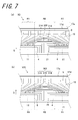
- a thermal head X3 in accordance with a third embodiment will be described with reference to FIG. 7 .
- a projection portion 202 When the thermal head X3 is seen in a plan view, a projection portion 202 has a triangular shape. Moreover, in a plan view, two oblique sides thereof define inclined parts 214.
- the projection portion 202 is placed, with its base located on the upstream side in the conveying direction S. That is, the projection portion 202 is so shaped that its area when seen in a plan view becomes narrower gradually toward the downstream side in the conveying direction S. In other words, the projection portion 202 is so shaped that the area of contact with the recording medium P becomes narrower gradually in the same direction.
- the projection portion 202 is so shaped that the area of contact with the recording medium P becomes narrower gradually toward the downstream side in the conveying direction S. This makes it possible to lessen a frictional force developed between the recording medium P and the projection portion 202, and thereby achieve smooth conveyance of the recording medium.
- the projection portion 202 has a triangular shape, and the two oblique sides thereof define the inclined parts 214, it is possible to achieve a gradual decrease in the area of contact between the recording medium P and the projection portion 202. Accordingly, the frictional force developed between the recording medium P and the projection portion 202 can be reduced gradually without causing a sharp decrease in the area of contact between the recording medium P and the projection portion 202. This helps decrease the possibility of occurrence of a sticking phenomenon.
- the inclined part 214 is inclined with respect to the sub scanning direction S, and, the angle which the inclined part 214 forms with the conveying direction S preferably falls in the range of 40 to 140°.
- the projection portion 202 is configured to have a triangular shape when seen in a plan view, it is possible to make efficient use of a space between the IC-IC connection electrodes 26, and thereby achieve downsizing of the thermal head X3.
- a projection portion 302 has a C-shape which is obtained by cutting a small trapezoid from a large trapezoid.
- the projection portion 302 comprises three sides, namely two oblique sides 314 and one side 315. A space surrounded by the two oblique sides 314 and the one side 315 is free of the projection portion 302.
- the one side 315 is disposed along the main scanning direction, and, the inclined part 314 is located at each end of the one side 315.
- the angle which one of the inclined parts 314 forms with the one side 315 and the angle which the other one of the inclined parts 314 forms with the one side 315 are equal to each other. Accordingly, the configuration of the projection portion 302 is line-symmetrical about a centerline of the projection portion 302 in the main scanning direction.
- the projection portion 302 is configured to support the recording medium P in a manner such that the sagging recording medium P can be upheld gradually from each end in the main scanning direction by the projection portion 302. Accordingly, as conveyance of the recording medium P proceeds, a central part of the recording medium P in the main scanning direction in a state of sagging down most deeply can be gradually lifted up by the projection portion 302. This makes it possible to smooth wrinkles while decreasing the possibility of occurrence of a large stress in the recording medium P without rapid elimination of wrinkles.
- a thermal head X4 in accordance with the third embodiment will be described with reference to FIG. 8 .
- the thermal head X4 includes a third projection portion 402a, a fourth projection portion 402b, and a fifth projection portion 402c. Moreover, the projection portion 402 is disposed on each of the IC-IC connection electrodes 26 that are electrically independent of each other.
- the third projection portion 402a, the fourth projection portion 402b, and the fifth projection portion 402c are arranged sequentially in the order named from the upstream side in the conveying direction S.
- the third projection portion 402a, the fourth projection portion 402b, and the fifth projection portion 402c are rectangular-shaped and have substantially the same size.
- the recording medium P is brought into contact with the third projection portion 402a, the fourth projection portion 402b, and the fifth projection portion 402c one after another in the order named. It is therefore possible to smooth wrinkles gradually from the third projection portion 402a toward the fifth projection portion 402c.
- the third projection portion 402a, the fourth projection portion 402b, and the fifth projection portion 402c are each disposed on the IC-IC connection electrode 26, wherefore the current carrying capacity of the IC-IC connection electrode 26 can be increased.
- the recording medium P is brought into contact with the projection portion 402 several times, wherefore a stress developed between the recording medium P and the projection portion 402 can be dispersed. Furthermore, since the third projection portion 402a, the fourth projection portion 402b, and the fifth projection portion 402c are disposed on their respective different IC-IC connection electrodes 26, it follows that the third projection portion 402a, the fourth projection portion 402b, and the fifth projection portion 402c are thermally independent of each other.
- the thermal head X3 is, as exemplified, configured so that the third projection portion 402a, the fourth projection portion 402b, and the fifth projection portion 402c are disposed on their respective different IC-IC connection electrodes 26, alternatively, the third projection portion 402a, the fourth projection portion 402b, and the fifth projection portion 402c may be disposed on a single IC-IC connection electrode 26. Also in this case, the current carrying capacity of the IC-IC connection electrode 26 can be increased.
- a projection portion 502 comprises a third projection portion 502a, a fourth projection portion 502b, and a fifth projection portion 502c that are arranged sequentially in the order named from the upstream side in the conveying direction S.
- the third projection portion 502a, the fourth projection portion 502b, and the fifth projection portion 502c are arranged in order of decreasing area.
- the thermal head is configured so that the area of contact between the recording medium P and the projection portion 502 becomes smaller gradually from the upstream side in the conveying direction S.
- the third projection portion 502a where the recording medium P is most strongly pressed against the projection portion 502 has the largest area of contact with the recording medium, and, the fourth projection portion 502b and the fifth projection portion 502c act to disperse a pressing force which diminishes gradually as the recording medium moves forward in the conveying direction S.
- the contacting area is adjusted in conformity with the pressing force exerted on the recording medium P, wherefore the recording medium P can be fed smoothly to the heat generating portion 9.
- the fifth projection portion 502c has the smallest area of contact with the recording medium P, wherefore the frictional force developed between the fifth projection portion 502c and the recording medium P can be kept small. Accordingly, the recording medium P can be separated from the fifth projection portion 502c smoothly.
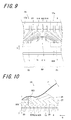
- a thermal head X5 implemented as the fifth embodiment will be described with reference to FIGS. 9 and 10 .
- the thermal head X5 differs from the thermal heads X1 to X4 in that a ground electrode 604 is disposed along the end face 7a of the substrate 7 so as to be surrounded by the end face 7a of the substrate 7, an IC-connector connection electrode 521, the individual electrode 19, and the IC-IC connection electrode 26.
- a convexity 606 is disposed on the ground electrode 604.
- a ground electrode 604 disposed below the convexity 606 is electrically connected to the ground electrode 604 extending along the end face 7a of the substrate 7 via a coupling electrode 614.
- the convexity 606 has a trapezoidal shape when seen in a plan view, and is made of the earlier described Ag paste. Therefore, a projection portion 604 has electrical conductivity, and is maintained at a ground potential.
- the convexity 606 is disposed so as to protrude from the cover layer 27, and the upper surface of the convexity 606 is left exposed from the cover layer 27. That is, the projection portion 602 is configured to have the exposed convexity 606.
- the recording medium P under conveyance is brought into contact with the upper surface of the convexity 606 left exposed from the cover layer 27.
- an electrically-conductive protective film (not shown) may be provided on the convexity 606.
- the convexity 606 and the electrically-conductive protective film constitute the projection portion 602.
- thermal printer Z1 employing the thermal head X1 according to the first embodiment has been shown herein, but this does not suggest any limitation, and thus the thermal heads X2 to X5 may be adopted for use in the thermal printer Z1.
- the thermal heads X1 to X5 according to several embodiments may be used in combination.
- the process of printing an Ag paste has been described as a way to form the thick electrode portion 17d and the convexity 2 following the formation of various electrodes, but this does not suggest any limitation.
- the protuberant portion 13b is formed in the heat storage layer 13, and the electrical resistance layer 15 is formed on the protuberant portion 13b, but this does not suggest any limitation.
- the heat generating portion 9 of the electrical resistance layer 15 may be placed on the underlayer portion 13b of the heat storage layer 13 without forming the protuberant portion 13b in the heat storage layer 13.
- the heat storage layer 13 may be formed over the entire area of the upper surface of the substrate 7.
- the protecting member 12 finds its way through the second exposed part 16 to the surface of the heat storage layer 13, wherefore the strength of adhesion between the substrate 7 and the protecting member 12 can be enhanced.
- the protecting member 12 and the covering member 29 which covers the driving IC 11 may be formed of the same material.
- the covering member 29 and the protecting member 12 can be formed together at one time by performing printing also on the protecting member 12-forming region during the printing process for forming the covering member 29.
- the covering member 29 is, as exemplified, disposed so as to straddle over a plurality of driving ICs 11, the covering member 29 may be provided for each of the driving ICs on an individual basis. In this case, the difference in height between the first region R1 and the second region R2 becomes more noticeable, wherefore it is possible to utilize the invention efficiently.
- the invention is applicable to an edge-type head in which the heat generating portion 9 is disposed on the end face of the substrate 7. Furthermore, the invention may adopt a turned-back pattern in which adjacent heat generating portions 9 are connected to each other by a turned-back electrode (not shown).
- the driving IC 11 is, as exemplified, flip-chip mounted on the substrate 7, but this does not suggest any limitation.
- the driving IC 11 may be disposed on the substrate 7 so as to be electrically connected to various electrodes by means of wire bonding.
- the head substrate 3 may be electrically connected to an external substrate without providing the connector 31, and thus, also in a case where an external substrate having the driving IC 11 disposed on an upper surface thereof is abutted on the head substrate 3 so that the head substrate 3 and the external substrate can be juxtaposed, and then the driving IC 11 is electrically connected to various electrodes by means of wire bonding, it is possible to utilize the invention efficiently.
Landscapes
- Engineering & Computer Science (AREA)
- Microelectronics & Electronic Packaging (AREA)
- Electronic Switches (AREA)
Abstract
Description
- The present invention relates to a thermal head and a thermal printer equipped with the thermal head.
- Various types of thermal heads have been proposed to date as printing devices for use in facsimiles, video printers, and so forth. For example, there is known a thermal head comprising: a substrate; a heat generating portion disposed on the substrate; a driving IC which controls actuation of the heat generating portion; and a covering member which covers the driving IC, the covering member serving also as an ink ribbon guide, in which a recording medium is conveyed while making contact with the covering member (refer to
Patent Literature 1, for example). Moreover, when the substrate is seen in a plan view, this thermal head is composed of a first region defined by extending a driving-IC disposed area in a sub scanning direction, and second regions which are regions other than the first region. - Patent Literature 1: Japanese Unexamined Patent Publication
JP-A 01-281956 (1989 - In the thermal head as above described, however, the height of the second region free of the driving IC is lower than the height of the first region, thus causing poor contacting condition between a recording medium and the thermal head, which gives rise to the possibility of occurrence of wrinkles in the recording medium.
- A thermal head in accordance with one embodiment of the invention comprises: a substrate; a heat generating portion disposed on the substrate; a driving IC which is disposed on the substrate and controls actuation of the heat generating portion; and a covering member which covers the driving IC. Moreover, when the substrate is seen in a plan view, the thermal head is composed of a first region defined by extending a driving-IC disposed area in a sub scanning direction, and second regions which are regions other than the first region. In addition, in the at least one of the second regions which lies closer to the heat generating portion than the driving-IC disposed area is provided a projection portion which makes contact with a recording medium under conveyance.
- A thermal printer in accordance with one embodiment of the invention comprises: the thermal head as described above; a conveyance mechanism which conveys the recording medium onto the heat generating portion; and a platen roller which presses the recording medium onto the heat generating portion.
- According to the invention, the possibility of causing wrinkles in a recording medium can be decreased.
-
-
FIG. 1 is a plan view showing a first embodiment of a thermal head according to the invention; -
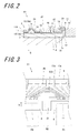
FIG. 2 is a sectional view taken along the line I-I shown inFIG. 1 ; -
FIG. 3 is an enlarged plan view of a vicinity of a projection portion of the thermal head shown inFIG. 1 ; -
FIG. 4 is a conceptual diagram illustrating a condition of contact between a recording medium and the thermal head shown inFIG. 1 , whereinFIG. 4(a) shows the vicinity of a driving IC, andFIG. 4(b) shows the vicinity of the projection portion; -
FIG. 5 is a view showing the general structure of the first embodiment of a thermal printer according to the invention; -
FIG. 6 is a plan view showing a second embodiment of the invention; -
FIG. 7 shows a thermal head in accordance with a third embodiment of the invention, whereinFIG. 7(a) is an enlarged plan view of the vicinity of the projection portion, andFIG. 7(b) is a plan view showing a modified example of the thermal head shown inFIG. 6(a) ; -
FIG. 8 shows a thermal head in accordance with a fourth embodiment of the invention, whereinFIG. 8(a) is an enlarged plan view of the vicinity of the projection portion, andFIG. 8(b) is a plan view showing a modified example of the thermal head shown inFIG. 7(a) ; -
FIG. 9 is an enlarged plan view of the vicinity of the projection portion in a thermal head in accordance with a fifth embodiment of the invention; and -
FIG. 10 is a conceptual diagram illustrating a contacting condition in the vicinity of the projection portion of the thermal head shown inFIG. 9 . - Hereinafter, a thermal head X1 will be described with reference to
FIGS. 1 to 4 . The thermal head X1 comprises: aheatsink 1; ahead substrate 3 placed on theheatsink 1; and aconnector 31 connected to thehead substrate 3. InFIG. 1 , the diagrammatic representation of theconnector 31 is omitted, and, a region where theconnector 31 is placed is indicated by alternate long and short dashed lines. - While the
connector 31 will hereafter be described as a connecting member which makes external electrical connection, other members having flexibility such as a flexible printed wiring board, a glass epoxy substrate, or a polyimide substrate, can be used instead. In a case where external electrical connection is established by a flexible printed wiring board, a reinforcing plate made of resin such for example as a phenol resin, a polyimide resin, or a glass epoxy resin (not shown in the drawing) may be disposed between the flexible printed wiring board and theheatsink 1. - The
heatsink 1 has the form of a plate, and, in a plan view, theheatsink 1 is rectangular-shaped. Theheatsink 1 is formed of a metal material such for example as copper, iron, or aluminum, and has the capability of dissipating, of heat generated by aheat generating portion 9 of thehead substrate 3, heat which is not responsible for printing. Moreover, thehead substrate 3 is bonded to the upper surface of theheatsink 1 by means of double-faced tape, an adhesive, or otherwise (not shown). - In a plan view, the
head substrate 3 has the form of a plate, and, constituent members of the thermal head X1 are each disposed on asubstrate 7 of thehead substrate 3. Thehead substrate 3 has the function of performing printing on a recording medium (not shown) in response to an electric signal issued from outside. - As shown in
FIGS. 1 and2 , theconnector 31 comprises: a plurality ofconnector pins 8; and ahousing 10 which accommodates the plurality ofconnector pins 8. The plurality ofconnector pins 8 have one sides left exposed outside of thehousing 10, and have other sides stored within thehousing 10. The plurality ofconnector pins 8 have the function of ensuring electrical conduction between each of various electrodes of thehead substrate 3 and an externally-disposed power supply, and are electrically independent of each other. Theconnector pins 8 are required to have electrical conductivity, and are therefore formed of a metal or an alloy. - The
housing 10 has the function of accommodating therespective connector pins 10 in a state of being electrically independent of each other, and is therefore formed of an insulating member. Thehousing 10 effects supply of electricity to thehead substrate 3 by means of attachment and detachment of an externally-disposed connector (not shown). Thehousing 10 is made of, for example, a thermosetting resin, an ultraviolet-curable resin, or a photo-curable resin. - Hereinafter, each of members constituting the
head substrate 3 will be described. - The
substrate 7 is formed of an electrically insulating material such as alumina ceramics, or a semiconductor material such as single-crystal silicon. - A
heat storage layer 13 is formed on the upper surface of thesubstrate 7. Theheat storage layer 13 comprises: anunderlayer portion 13a; and aprotuberant portion 13b. Theunderlayer portion 13a is formed over the left half of the upper surface of thesubstrate 7. Theprotuberant portion 13b extends in the form of a strip along a main scanning direction of a plurality ofheat generating portions 9, and has a substantially semi-elliptical sectional profile. Theunderlayer portion 13a is disposed near theheat generating portion 9 while being located below aprotective layer 25 which will hereafter be described. Theprotuberant portion 13b acts to press a recording medium which is subjected to printing against theprotective layer 25 formed on theheat generating portion 9 in a satisfactory manner. - The
heat storage layer 13 is formed of glass having a low heat conductivity, and accumulates part of heat generated by theheat generating portion 9 temporarily. Accordingly, theheat storage layer 13 is able to shorten the time required for a temperature rise in theheat generating portion 9, and thus acts to improve the thermal response characteristics of the thermal head X1. - For example, the
heat storage layer 13 is formed by applying a predetermined glass paste, which is obtained by blending a suitable organic solvent in glass powder, onto the upper surface of thesubstrate 7 by means of heretofore known screen printing or otherwise, and subsequently firing the paste. - An
electrical resistance layer 15 is disposed on the upper surface of theheat storage layer 13, and, on theelectrical resistance layer 15 are disposed aground electrode 4, acommon electrode 17, anindividual electrode 19, an IC-connector connection electrode 21, and an IC-IC connection electrode 26. Theelectrical resistance layer 15 is subjected to patterning so as to have the same shape as theground electrode 4, thecommon electrode 17, theindividual electrode 19, the IC-connector connection electrode 21, and the IC-IC connection electrode 26, and has an exposed region serving as an exposed electrical-resistance layer 15 region lying between thecommon electrode 17 and theindividual electrode 19. - As shown in
FIG. 1 , there are arranged exposed regions of the electrical-resistance layer 15 in an array on theprotuberant portion 13b of theheat storage layer 13, and, each of the exposed regions constitutes theheat generating portion 9. The plurality ofheat generating portions 9, while being illustrated in simplified form inFIG. 1 for convenience in explanation, are arranged at a density of 100 dpi to 2400 dpi (dot per inch), for example. Theelectrical resistance layer 15 is formed of a material having a relatively high electrical resistance such for example as a TaN-based material, a TaSiO-based material, a TaSiNO-based material, a TiSiO-based material, a TiSiCO-based material, or a NbSiO-based material. Thus, upon application of a voltage to theheat generating portion 9, theheat generating portion 9 is caused to generate heat under Joule heating effect. - The
ground electrode 4, thecommon electrode 17, theindividual electrode 19, the IC-connector connection electrode 21, and the IC-IC connection electrode 26 are formed of a material having electrical conductivity, for example, one metal material selected from among aluminum, gold, silver, and copper, or an alloy of these metals. - The
common electrode 17 comprises: amain wiring portion 17a; asub wiring portion 17b; alead portion 17c; and athick electrode portion 17d. Themain wiring portion 17a extends along one long side of thesubstrate 7. Thesub wiring portion 17b extends along each of one and the other short sides of thesubstrate 7. Thelead portion 17c extends from themain wiring portion 17a toward each of theheat generating portions 9. Thethick electrode portion 17d, which is disposed on themain wiring portion 17a and thesub wiring portion 17b, is made thicker than the other portions of thecommon electrode 17. Thecommon electrode 17 provides electrical connection between theconnector 31 and each of theheat generating portions 9. - The thermal head X1 is configured so that an electric current fed from the
sub wiring portion 17b located at each end thereof in the direction of arrangement of the heat generating portions 9 (hereafter also referred to as "main scanning direction") passes through themain wiring portion 17a, flows through each of thelead portions 17c, and is thereby supplied to each of theheat generating portions 9. On themain wiring portion 17a, as well as on thesub wiring portion 17b, there is provided thethick electrode portion 17d which acts to increase the current carrying capacity of themain wiring portion 17a and thesub wiring portion 17b. Exemplary of thethick electrode portion 17d is an Ag paste. - A plurality of
individual electrodes 19 provide electrical connection between each of theheat generating portions 9 and a drivingIC 11. Moreover, given that theheat generating portions 9 are bunched together in groups, theindividual electrodes 19 allow theheat generating portions 9 in each group to make electrical connection with a corresponding one of the drivingICs 11 prepared for the heat generating portion groups, respectively. - A plurality of IC-
connector connection electrodes 21 have one ends connected to the drivingIC 11 and have other ends led out to anend face 7a of thesubstrate 7. The led-out ends are electrically connected to theconnector 31, thereby permitting electrical connection between the drivingIC 11 and theconnector 31. The plurality of IC-connector connection electrodes 21 connected to each of the drivingIC 11 are configured by a plurality of wiring lines having different functions. - The
ground electrode 4, which is placed between the IC-connector connection electrode 21 and themain wiring portion 17a of thecommon electrode 17, has a large area. Theground electrode 4 is grounded and maintained at a potential of 0 to 1 V. - A plurality of IC-
IC connection electrodes 26 provide electrical connection between the drivingICs 11 arranged adjacent each other. The plurality of IC-IC connection electrodes 26 are disposed in correspondence to the IC-connector connection electrodes 21, and transmit various signals to the adjacent drivingICs 11. That is, an electric current is fed from theconnector 31 to the drivingIC 11 by way of the IC-connector connection electrodes 21 and the IC-IC connection electrodes 26. - As shown in
FIG. 1 , the drivingIC 11 is placed in correspondence to each of the groups including the plurality ofheat generating portions 9, and is connected to theindividual electrode 19, the IC-connector connection electrode 21, and theground electrode 4. The drivingIC 11 has the function of controlling the current-carrying state of each of theheat generating portions 9. It is advisable to use a switching member having a plurality of built-in switching elements as the drivingIC 11. - As shown in
FIG. 1 , when thesubstrate 7 is seen in a plan view, in a sub scanning direction S coincident with a conveying direction S in which a recording medium (not shown) is conveyed, the thermal head X1 is composed of a first region R1 defined by extending a driving-IC 11 disposed area in the sub scanning direction, and second regions R2 which are regions other than the first region R1. - The first region R1 has a width which is equal to the width of the driving
IC 11 in the main scanning direction, and extends along the sub scanning direction S while maintaining the width. In other words, in a plan view, the first region R1 is a region defined by virtual lines extending in the sub scanning direction S along side faces of the drivingIC 11 that are perpendicular to the main scanning direction. - The
electrical resistance layer 15, thecommon electrode 17, theindividual electrode 19, theground electrode 4, the IC-connector connection electrode 21, and the IC-IC connection electrode 26 thus far described are formed by, for example, stacking layers of their constituent materials on theheat storage layer 13 one after another by a heretofore known thin-film forming technique such as a sputtering method, and subsequently working the resultant layered body into predetermined patterns by a heretofore known technique such as a photo-etching method. Note that thecommon electrode 17, theindividual electrode 19, theground electrode 4, the IC-connector connection electrode 21, and the IC-IC connection electrode 26 can be formed at one time through the same process steps. Meanwhile, thethick electrode portion 17d can be formed by means of printing before or after the process of working the different electrodes into predetermined patterns. - As shown in
FIGS. 1 and2 , theprotective layer 25 which covers theheat generating portion 9, part of thecommon electrode 17, and part of theindividual electrode 19, is formed on theheat storage layer 13 formed on the upper surface of thesubstrate 7. InFIG. 1 , for convenience in explanation, a region where theprotective layer 25 is formed is indicated by alternate long and short dashed lines, and its diagrammatic representation is omitted. - The
protective layer 25 is intended to protect the covered areas of theheat generating portion 9, thecommon electrode 17, and theindividual electrode 19 against corrosion caused by adhesion of, for example, atmospheric water content, or against wear caused by contact with a recording medium which is subjected to printing. - The
protective layer 25 can be formed from SiN, SiO, SiON, SiC, SiCN, diamond-like carbon, or the like, and, theprotective layer 25 may either be of a single layer or be composed of a stack of layers. Such aprotective layer 25 can be produced by a thin-film forming technique such as the sputtering method, or a thick-film forming technique such as a screen printing method. - Moreover, as shown in
FIGS. 1 and2 , acover layer 27 which partly covers theground electrode 4, thecommon electrode 17, theindividual electrode 19, and the IC-connector connection electrode 21 is disposed on thesubstrate 7. InFIG. 1 , for convenience in explanation, a region where thecover layer 27 is formed is indicated by alternate long and short dashed lines. - The
cover layer 27 is intended to protect the covered areas of theground electrode 4, thecommon electrode 17, theindividual electrode 19, the IC-IC connection electrode 26, and the IC-connector connection electrode 21 against oxidation caused by contact with air, or corrosion caused by adhesion of atmospheric water content, for example. - In order to provide more secure protection for the
common electrode 17 and theindividual electrode 19, as shown inFIG. 2 , it is preferable that thecover layer 27 is so formed as to overlie an end part of theprotective layer 25. Thecover layer 27 can be formed from a resin material such for example as an epoxy resin or a polyimide resin using a thick-film forming technique such as the screen printing method. - The
cover layer 27 is formed with an opening (not shown) for leaving theindividual electrode 19, the IC-IC connection electrode 26, and the IC-connector connection electrode 21 connected to the drivingIC 11 exposed, so that the wiring lines can be connected to the drivingIC 11 through the opening. Moreover, the drivingIC 11 is, in a state of being connected to theindividual electrode 19, the IC-IC connection electrode 26, and the IC-connector connection electrode 21, covered with a coveringmember 29 formed of resin such for example as an epoxy resin or a silicone resin for the sake of protection of the drivingIC 11 and also protection of the area of connection between the drivingIC 11 and the wiring lines. In the present embodiment, the coveringmember 29 is disposed so as to straddle over a plurality of drivingICs 11. The height of thecover layer 27 from thesubstrate 7 can be determined as appropriate in accordance with the form of the thermal head X1, and, a desirable range of the height is from 200 to 500 µm. - As shown in
FIG. 2 , at that side of thecover layer 27 located toward theend face 7a of the main surface (not shown) of thesubstrate 7, the ends drawn from the different electrodes are exposed from an exposed area where the different electrodes are left exposed (not shown) so as to be electrically connected to theconnector 31. - The
connector 31 is disposed on thesubstrate 7, and, theconnector pin 8 is electrically connected to the led-out ends of the different electrodes by an electrically-conductive member 23. In the thermal head X1, theconnector 31 is disposed at each of the opposite ends and the midportion of the thermal head X1 in the main scanning direction. Exemplary of the electrically-conductive member 23 are solder and an anisotropic conductive adhesive obtained by blending conductive particles in an electrically insulating resin. Note that a Ni-, Au-, or Pd-plating layer (not shown) may be disposed between the electrically-conductive member 23 and the led-out ends of the different electrodes. - The thermal head X1 is provided with a protecting
member 12 which protects, at least partly, theconnector 31. The protectingmember 12 is disposed so as to cover theconnector pin 8, part of the upper surface of thehousing 10, and part of thecover layer 27, as well as to cover the exposed area completely when seen in a plan view. - The protecting
member 12 can be formed of a thermosetting resin, a thermosoftening resin, an ultraviolet-curable resin, or a visible light-curable resin, for example. Moreover, in a case where the different electrodes need to be electrically independent of each other, it is preferable that the protectingmember 12 has an electrically insulating property. - Moreover, the protecting
member 12 covers theconnector pin 8 of theconnector 31 which assures the electrical conduction, and, preferably, the protectingmember 12 is disposed also on part of the upper surface of thehousing 10. By doing so, theconnector pin 8 can be entirely covered with the protectingmember 12, thereby assuring the electrical conduction more positively. - Referring to
FIGS. 3 and4 , aprojection portion 2 will be described in detail.FIG. 3 shows the vicinity of theprojection portion 2 in an enlarged manner, andFIG. 4 is a conceptual diagram illustrating a condition of contact between a recording medium P and the coveringmember 29, as well as theprojection portion 2. A solid line drawn inFIGS. 4(a) and 4(b) indicates a position of conveyance of the recording medium P in the present embodiment, whereas a broken line drawn inFIG. 4(b) indicates a position of conveyance of the recording medium P in a case where theprojection portion 2 is assumed to be absent. - As shown in
FIG. 3 , theprojection portion 2 is disposed at a center of thesubstrate 7 in the main scanning direction so as to lie in the second region R2. Moreover, theprojection portion 2 is disposed in a position spaced downstream from the drivingIC 11 in the conveying direction S of the recording medium P. Furthermore, theprojection portion 2 is located in at least one of the second regions R2 which lies closer to theheat generating portion 9 than the driving-IC 11 disposed area. - The IC-
connector connection electrode 21 and the IC-IC connection electrode 26 are arranged around theprojection portion 2, and thus theprojection portion 2 is placed so as to be surrounded by the IC-connector connection electrode 21 and the IC-IC connection electrode 26. - As shown in
FIG. 4 , aconvexity 6 is disposed below theprojection portion 2, and, thecover layer 27 is situated over theconvexity 6. Thecover layer 27 covers not only theconvexity 6, but also the vicinity of theconvexity 6. Thus, theprojection portion 2 is composed of theconvexity 6 and thecover layer 27. Note that theconvexity 6 is disposed so as not to make contact with the IC-connector connection electrode 21 and the IC-IC connection electrode 26. That is, theconvexity 6 is electrically isolated from the IC-connector connection electrode 21 and the IC-IC connection electrode 26. - The
convexity 6 can be formed of a material similar to the material constituting thethick electrode portion 17d. Moreover, theconvexity 6 can be formed by means of printing. Therefore, by forming theconvexity 6 concurrently with the formation of thethick electrode portion 17d, it is possible to achieve shortening of takt time, and thereby increase the manufacturing efficiency. Note that theconvexity 6 may also be formed by raising part of thesubstrate 7. - It is preferable that the height of the
convexity 6 from thesubstrate 7 falls in the range of 15 to 30 µm. Theprojection portion 2 has a rectangular shape when seen in a plan view, and its height h3 from thesubstrate 7 preferably falls in the range of 40 to 70 µm. Moreover, theprojection portion 2 is preferably given a surface roughness greater than the surface roughness of other area of thecover layer 27 than theprojection portion 2. This makes it possible to render the recording medium P less slippery, and thereby improve the condition of intimate contact between the projection portion and the recording medium under conveyance. - A height h1 of the covering
member 29 from thesubstrate 7 in the first region R1 is greater than a height h2 of the coveringmember 29 from thesubstrate 7 in the second region R2. This is ascribable to the presence or absence of the drivingIC 11 located in a lower part of the coveringmember 29. Note that the height h1, h2 of the coveringmember 29 from thesubstrate 7 refers to the level of the vertex of the coveringmember 29 situated above the drivingIC 11, namely the height of that part of the covering member which is contacted by the recording medium P from thesubstrate 7. - It is preferable that the height h1 of the covering
member 29 from thesubstrate 7 falls in the range of 300 to 500 µm. Moreover, the height h2 of the coveringmember 29 from thesubstrate 7 preferably falls in the range of 200 to 400 µm. This makes it possible to support the conveyance of the recording medium P. - In measurement of height from the
substrate 7, for example, with use of a contact type or non-contact type surface roughness meter, a distance from a reference point can be measured. For example, the vertex of theprotuberant portion 13b of theheat storage layer 13 can be defined as the reference point. The surface roughness of theprojection portion 2 and that of thecover layer 27 can be also measured by a similar method. - Among various members constituting the thermal head X1, and, particularly among the members disposed on the
substrate 7, the drivingIC 11 has a noticeably large size. Therefore, the level of the surface of that part of the thermal head X1 which is provided with the drivingIC 11 and the level of the surface of that part of the thermal head X1 which is free of the drivingIC 1 differ greatly from each other. - Also in the case where the covering
member 29 is so disposed as to straddle over the plurality of drivingICs 11 as shown inFIG. 1 , the first region R1 is greater in height than the second region R2. The recording medium P is conveyed while making contact with the coveringmember 29, and, in the first region R1, the recording medium P is maintained at a predetermined level under the support of the coveringmember 29. - However, in a conventional thermal head devoid of the
projection portion 2, since the height h1, h2 of the coveringmember 29 from thesubstrate 7 varies depending on the presence or absence of the drivingIC 11 located in a lower part thereof, it follows that the condition of conveyance of the recording medium P in the first region R1 differs from that in the second region R2. That is, in the second region R2, as indicated by the chain-dotted line shown inFIG. 4(b) , the recording medium P may sag down, which leads to a difference in recording medium P-to-coveringmember 29 distance between the first region R1 and the second region R2. Therefore, the first region R1 and the second region R2 differ from each other in the condition of conveyance of the recording medium P. This gives rise to the possibility of causing wrinkles in the recording medium P which is being carried over the second region R2. - In contrast, in the thermal head X1, the
projection portion 2 is provided in at least one of the second regions R2 which lies closer to theheat generating portion 9 than the driving-IC 11 disposed area, and, theprojection portion 2 can make contact with the recording medium P. Thus, as indicated by the solid line inFIG. 4(b) , theprojection portion 2 is able to lift up the sagging recording medium P. This makes it possible to restrain the recording medium P against sagging motion, and thereby render the condition of conveyance of the recording medium P approximately uniform, wherefore the possibility of causing wrinkles in the recording medium P can be decreased. - Moreover, since the recording medium P makes contact with the covering
member 29 and theprojection portion 2, the recording medium P is supported at two points. Therefore, even if the coveringmember 29 and theprojection portion 2 are subjected to a stress when pressed by the recording medium P, the stress can be dispersed. - Moreover, in the process of performing sputtering of the
protective layer 25, there may be a case where a plurality of thermal heads X1 are stacked while being displaced from each other by a predetermined distance so that theirprotective layers 25 can be formed at one time. In this case, theprojection portion 2 acts to decrease the possibility of causing damage to the electrodes and so forth due to the overlapping arrangement of the thermal heads X1. More specifically, at the time of stacking the thermal heads X1 one upon another, by placing each thermal head X1 on theprojection portion 2, a space can be formed between the stacked thermal heads X1. This space helps protect the electrodes and so forth. - Moreover, the
projection portion 2 is placed in a position spaced downstream from the drivingIC 11 in the conveying direction S of the recording medium P. Accordingly, the recording medium P is brought into contact with theprojection portion 2 after making contact with the coveringmember 29 located above the drivingIC 11. Thus, the recording medium P can be stably supported by the coveringmember 29, and also, the recording medium P in a state of sagging down in a region between the drivingIC 11 and theheat generating portion 9 can be upheld at a predetermined level by theprojection portion 2. As a result, the recording medium P can be conveyed smoothly to theheat generating portion 9. - Moreover, since the
projection portion 2 is located between the coveringmember 29 and theheat generating portion 9, it follows that the recording medium P is brought into contact with theprojection portion 2 after making contact with the coveringmember 29. Accordingly, the recording medium P which is being carried toward theheat generating portion 9 can be upheld at a predetermined level, with consequent accomplishment of smooth conveyance of the recording medium P to theheat generating portion 9. In addition, theprojection portion 2 ensures more stable conveyance of the recording medium P to theheat generating body 9. - The height h3 of the
projection portion 2 from thesubstrate 7 is shorter than the height h1, h2 of the coveringmember 29 from thesubstrate 7. Thus, the recording medium P is supported by thetaller covering member 29, thereby achieving stable conveyance of the recording medium P. This is because the coveringmember 29 is greater in volume and strength than theprojection portion 2. - Moreover, in the conveying direction S, the height h3 of the
projection portion 2 located on the downstream side from thesubstrate 7 is shorter than the height h2 of the drivingIC 11 located on the upstream side in the second region R2 from thesubstrate 7. Accordingly, also in the second region R2, the recording medium P can be supported by the coveringmember 29, and theprojection portion 2 is able to convey the recording medium P smoothly to theheat generating portion 9. - Moreover, it is preferable that the distance between the
projection portion 2 and theheat generating portion 9 is 0.3 to 0.8 time the distance between the coveringmember 29 and theheat generating portion 9, and that the height h3 of theprojection portion 2 from thesubstrate 7 is 0.05 to 0.3 time the height h1, h2 of the coveringmember 29 from thesubstrate 7. - By fulfilling the above prescribed ranges, it is possible to suppress an excessive increase in the area of contact between the recording medium P and the
projection portion 2, and thereby permit adequate contact of the recording medium P with theprojection portion 2. Accordingly, conveyance of the recording medium P can be effected satisfactorily. Moreover, it is more preferable that the distance between theprojection portion 2 and theheat generating portion 9 is 0.4 to 0.6 time the distance between the coveringmember 29 and theheat generating portion 9, and that the height h3 of theprojection portion 2 from thesubstrate 7 is 0.1 to 0.2 time the height h1, h2 of the coveringmember 29 from thesubstrate 7. - The distance between the covering
member 29 and theheat generating portion 9 refers to a distance between the coveringmember 29 and theheat generating portion 9 arranged on a straight line extending along the sub scanning direction, and more specifically a distance between a side of the coveringmember 29 nearest theheat generating portion 9 and a virtual line extending along the main scanning direction while passing through the center of theheat generating portion 9. - For example, the condition of contact of the covering
member 29 and theprojection portion 2 with the recording medium P can be checked by the following method. To begin with, a coating of paint is applied to the surfaces of the coveringmember 29 and theprojection portion 2, and then conveyance of the recording medium P is effected. Whether or not the coveringmember 29 and theprojection portion 2 have made contact with the recording medium P can be checked by examining the presence or absence of the paint coating on the surfaces of the coveringmember 29 and theprojection portion 2. - The
projection portion 2 is, as exemplified, composed of theconvexity 6 and thecover layer 27, but it is not so limited. For example, theprojection portion 2 may be composed solely of theconvexity 6 without providing thecover layer 27 over theconvexity 6. In another alternative, theprojection portion 2 may be formed by laminatingseveral cover layers 27 one after another. In this case, theprojection portion 2 can be composed solely of thecover layer 27. - Next, a thermal printer Z1 will be described with reference to
FIG. 5. FIG. 5 is a view showing the general features of the thermal printer Z1, wherein the thermal head X1 is illustrated as being larger than its actual size. - As shown in
FIG. 5 , the thermal printer Z1 of the present embodiment comprises: the thermal head X1 thus far described; aconveyance mechanism 40; aplaten roller 50; a power-supply device 60; and acontrol device 70. The thermal head X1 is attached to a mountingsurface 80a of a mountingmember 80 disposed in a casing (not shown in the drawing) for the thermal printer Z1. - The
conveyance mechanism 40 comprises: a driving section (not shown); and conveyingrollers conveyance mechanism 40 is intended to convey the recording medium P such as thermal paper or ink-transferable image-receiving paper in a direction indicated by arrow S shown in the drawing so that the recording medium P can be conveyed onto theprotective layer 25 situated on the plurality ofheat generating portions 9 of the thermal head X1. The driving section has the function of driving the conveyingrollers roller cylindrical shaft body elastic member heat generating portion 9 of the thermal head X1, and thus the recording medium P and the ink film are conveyed together. - The
platen roller 50 has the function of pressing the recording medium P onto theprotective layer 25 situated on theheat generating portion 9 of the thermal head X1. Theplaten roller 50 is disposed so as to extend along a direction perpendicular to the conveying direction S of the recording medium P, and is fixedly supported at its ends so that it is able to rotate while pressing the recording medium P onto theheat generating portion 9. For example, theplaten roller 50 can be constructed of acylindrical shaft body 50a formed of metal such as stainless steel covered with anelastic member 50b formed of butadiene rubber or the like. - The power-
supply device 60 has the function of supplying electric current for allowing theheat generating portion 9 of the thermal head X1 to generate heat, as well as electric current for operating the drivingIC 11. Thecontrol device 70 has the function of feeding a control signal for controlling the operation of the drivingIC 11 to the drivingIC 11 in order for theheat generating portions 9 of the thermal head X1 to generate heat in a selective manner. - In the thermal printer Z1, as shown in
FIG. 5 , the recording medium P is conveyed onto theheat generating portions 9 of the thermal head X1 by theconveyance mechanism 40 while being pressed onto theheat generating portions 9 by theplaten roller 50, and, theheat generating portions 9 are caused to generate heat in a selective manner by the power-supply device 60 and thecontrol device 70, whereby predetermined printing can be performed on the recording medium P. In a case where the recording medium P is image-receiving paper or the like, printing is performed on the recording medium P by effecting thermal transfer of the ink of an ink film (not shown) which is being conveyed together with the recording medium P onto the recording medium P. - A thermal head X2 in accordance with a second embodiment will be described with reference to
FIG. 6. FIG. 6 is a plan view showing an electrode pattern of the thermal head. The diagrammatic representations of the protective film, the cover layer, and the connector are omitted, and, the coveringmember 29 is indicated by alternate long and short dashed lines. InFIG. 6 , except for a projection portion 102, the other constituent components are similar to those of the foregoing embodiment, and thus the description thereof will be omitted. In what follows, similar reference characters are used to denote like members. - The projection portion 102 comprises a
first projection portion 102a and asecond projection portion 102b. Thefirst projection portion 102a is located at a center of the thermal head X2 in the main scanning direction, and has the same configuration as that of theprojection portion 2 of the thermal head X1. Thesecond projection portion 102b is located at each end of the thermal head X2 in the main scanning direction. Thesecond projection portion 102b is formed integrally with athick electrode portion 117d provided on asub wiring portion 17b. - In this construction, printing is performed on the recording medium P in a state of being pressed against the thermal head X2 by the platen roller 50 (refer to
FIG. 5 ). Theplaten roller 50 exhibits a greater pressing force at its ends than at other area in the main scanning direction, because theshaft body 50a of theplaten roller 50 is fixed at its ends in the main scanning direction. Therefore, chances of occurrence of wrinkles in the recording medium P are increased in the second region R2 located at each end of the thermal head X2 in the main scanning direction. - However, in the thermal head X2, The projection portion 102 comprises the
first projection portion 102a and thesecond projection portion 102b. Since thesecond projection portion 102b acts to support the recording medium P so as to restrain the recording medium P against sagging motion, it is possible to decrease the possibility of causing wrinkles in the recording medium P. Moreover, thesecond projection portion 102b also acts to lessen the pressing force of theplaten roller 50, wherefore the pressing force distribution in the main scanning direction can be rendered approximately uniform. - The
first projection portion 102a is placed in a region formed on thesubstrate 7 by extending the region bearing an array of theheat generating portions 9 in the sub scanning direction S. On the other hand, thesecond projection portion 102b is placed in a region other than the region formed on thesubstrate 7 by extending the region bearing an array of theheat generating portions 9 in the sub scanning direction S. Therefore, in the main scanning direction, the distance between thesecond projection portion 102b and theheat generating portion 9 is greater than the distance between thefirst projection portion 102a and theheat generating portion 9. - The thermal head X2 is configured so that a distance Lb between the
heat generating portion 9 and thesecond projection portion 102b in the sub scanning direction is shorter than a distance La between theheat generating portion 9 and thefirst projection portion 102a in the sub scanning direction. Accordingly, thesecond projection portion 102b is located close to theheat generating portion 9, and is therefore able to support the recording medium P which is being carried in the vicinity of theheat generating portion 9. In this way, the recording medium P can be conveyed smoothly to theheat generating portion 9. - It is preferable that the distance La between the
heat generating portion 9 and thefirst projection portion 102a falls in the range of 3 to 5 mm, and that the distance Lb between theheat generating portion 9 and thesecond projection portion 102b falls in the range of 2.5 to 4.5 mm. This makes it possible to support the recording medium P which is being conveyed in the vicinity of theheat generating portion 9. - Moreover, the thermal head X2 is configured so that a width Wb of the
second projection portion 102b is greater than a width Wa of thefirst projection portion 102a. This makes it possible to increase the area of thesecond projection portion 102b when seen in a plan view which is subjected to a great pressing force exerted by theplaten roller 50. Accordingly, thesecond projection portion 102b is able to lessen the pressing force of theplaten roller 50, wherefore the possibility of causing wrinkles in the recording medium P can be decreased. Note that the width Wb of thesecond projection portion 102b coincides with the length of thesecond projection portion 102b in the main scanning direction, and the width Wa of thefirst projection portion 102a coincides with the length of thefirst projection portion 102a in the main scanning direction. - It is preferable that the width Wa falls in the range of 0.5 to 1.5 µm, and that the width Wb falls in the range of 2 to 6 µm. This makes it possible to suppress variations in the condition of conveyance of the recording medium P in the main scanning direction, and thereby decrease the possibility of causing wrinkles in the recording medium P.
- Moreover, the thermal head X2 is configured so that the length of the
first projection portion 102b in the sub scanning direction is greater than the length of thefirst projection portion 102a in the sub scanning direction. This makes it possible to increase the area of thesecond projection portion 102b when seen in a plan view which is subjected to a great pressing force exerted by theplaten roller 50. Accordingly, thesecond projection portion 102b is able to lessen the pressing force of theplaten roller 50, wherefore the possibility of causing wrinkles in the recording medium P can be decreased. - It is preferable that the length of the
second projection portion 102b falls in the range of 1.5 to 2.5 µm, and that the length of thefirst projection portion 102a falls in the range of 0.5 to 1.5 µm. This makes it possible to suppress variations in the condition of conveyance of the recording medium P in the main scanning direction, and thereby decrease the possibility of causing wrinkles in the recording medium P. - It is noted that the distance La between the
heat generating portion 9 and thefirst projection portion 102a in the sub scanning direction may be shorter than the distance Lb between theheat generating portion 9 and thesecond projection portion 102b in the sub scanning direction. In fact, in the process of forming various electrode patterns, there may be a case where a region capable of placement of thefirst projection portion 102a is smaller than a region capable of placement of thesecond projection portion 102b. - In this case, the
first projection portion 102a cannot be made larger than thesecond projection portion 102b, wherefore the volume of an Ag paste forming thefirst projection portion 102a is smaller than the volume of an Ag paste forming thesecond projection portion 102b. - Accordingly, the
first projection portion 102a is less heat storable than thesecond projection portion 102b, and can therefore be placed closer to the figureheat generating portion 9. As a result, thefirst projection portion 102a is able to convey the recording medium P smoothly to theheat generating portion 9. - Moreover, in the thermal head X2, the width Wa of the
first projection portion 2 may be shorter than the width Wb of thesecond projection portion 2. In this case, thesecond projection portion 2 is able to lessen the pressing force of theplaten roller 50 effectively, wherefore the possibility of causing wrinkles in the recording medium P can be decreased. - A thermal head X3 in accordance with a third embodiment will be described with reference to
FIG. 7 . - When the thermal head X3 is seen in a plan view, a
projection portion 202 has a triangular shape. Moreover, in a plan view, two oblique sides thereof defineinclined parts 214. Theprojection portion 202 is placed, with its base located on the upstream side in the conveying direction S. That is, theprojection portion 202 is so shaped that its area when seen in a plan view becomes narrower gradually toward the downstream side in the conveying direction S. In other words, theprojection portion 202 is so shaped that the area of contact with the recording medium P becomes narrower gradually in the same direction. - Thus, the
projection portion 202 is so shaped that the area of contact with the recording medium P becomes narrower gradually toward the downstream side in the conveying direction S. This makes it possible to lessen a frictional force developed between the recording medium P and theprojection portion 202, and thereby achieve smooth conveyance of the recording medium. - In particular, since the
projection portion 202 has a triangular shape, and the two oblique sides thereof define theinclined parts 214, it is possible to achieve a gradual decrease in the area of contact between the recording medium P and theprojection portion 202. Accordingly, the frictional force developed between the recording medium P and theprojection portion 202 can be reduced gradually without causing a sharp decrease in the area of contact between the recording medium P and theprojection portion 202. This helps decrease the possibility of occurrence of a sticking phenomenon. - It is sufficient that, when the
substrate 7 is seen in a plan view, theinclined part 214 is inclined with respect to the sub scanning direction S, and, the angle which theinclined part 214 forms with the conveying direction S preferably falls in the range of 40 to 140°. Moreover, by configuring theprojection portion 202 to have a triangular shape when seen in a plan view, it is possible to make efficient use of a space between the IC-IC connection electrodes 26, and thereby achieve downsizing of the thermal head X3. - Referring to
FIG. 6(b) , a modified example of the thermal head X3 will be described. When the thermal head X3 is seen in a plan view, aprojection portion 302 has a C-shape which is obtained by cutting a small trapezoid from a large trapezoid. Theprojection portion 302 comprises three sides, namely twooblique sides 314 and oneside 315. A space surrounded by the twooblique sides 314 and the oneside 315 is free of theprojection portion 302. - The one
side 315 is disposed along the main scanning direction, and, theinclined part 314 is located at each end of the oneside 315. The angle which one of theinclined parts 314 forms with the oneside 315 and the angle which the other one of theinclined parts 314 forms with the oneside 315 are equal to each other. Accordingly, the configuration of theprojection portion 302 is line-symmetrical about a centerline of theprojection portion 302 in the main scanning direction. - The
projection portion 302 is configured to support the recording medium P in a manner such that the sagging recording medium P can be upheld gradually from each end in the main scanning direction by theprojection portion 302. Accordingly, as conveyance of the recording medium P proceeds, a central part of the recording medium P in the main scanning direction in a state of sagging down most deeply can be gradually lifted up by theprojection portion 302. This makes it possible to smooth wrinkles while decreasing the possibility of occurrence of a large stress in the recording medium P without rapid elimination of wrinkles. - It is possible to dispose the IC-
IC connection electrode 26 in the projection portion 302-free space surrounded by the twooblique sides 314 and the oneside 315. That is, by providing the IC-IC connection electrode 26 in the space surrounded by the twooblique sides 314 and the oneside 315, it is possible to increase the area of the IC-IC connection electrode 26, and thereby decrease interconnection resistance. - A thermal head X4 in accordance with the third embodiment will be described with reference to
FIG. 8 . - The thermal head X4 includes a
third projection portion 402a, afourth projection portion 402b, and afifth projection portion 402c. Moreover, theprojection portion 402 is disposed on each of the IC-IC connection electrodes 26 that are electrically independent of each other. - In the
projection portion 402, thethird projection portion 402a, thefourth projection portion 402b, and thefifth projection portion 402c are arranged sequentially in the order named from the upstream side in the conveying direction S. In a plan view, thethird projection portion 402a, thefourth projection portion 402b, and thefifth projection portion 402c are rectangular-shaped and have substantially the same size. - In the
projection portion 402, the recording medium P is brought into contact with thethird projection portion 402a, thefourth projection portion 402b, and thefifth projection portion 402c one after another in the order named. It is therefore possible to smooth wrinkles gradually from thethird projection portion 402a toward thefifth projection portion 402c. Moreover, thethird projection portion 402a, thefourth projection portion 402b, and thefifth projection portion 402c are each disposed on the IC-IC connection electrode 26, wherefore the current carrying capacity of the IC-IC connection electrode 26 can be increased. - Moreover, the recording medium P is brought into contact with the
projection portion 402 several times, wherefore a stress developed between the recording medium P and theprojection portion 402 can be dispersed. Furthermore, since thethird projection portion 402a, thefourth projection portion 402b, and thefifth projection portion 402c are disposed on their respective different IC-IC connection electrodes 26, it follows that thethird projection portion 402a, thefourth projection portion 402b, and thefifth projection portion 402c are thermally independent of each other. - Accordingly, it is possible to increase the quantity of heat absorbed into the
projection portion 402 from the recording medium P when the recording medium P is brought into contact with theprojection portion 402. That is, in the case where thethird projection portion 402a, thefourth projection portion 402b, and thefifth projection portion 402c are disposed on their respective different IC-IC connection electrodes 26, as compared with a case where the recording medium is brought into contact with theprojection portion 402 in a single-piece form, improved heat dissipation capability can be attained. - While the thermal head X3 is, as exemplified, configured so that the
third projection portion 402a, thefourth projection portion 402b, and thefifth projection portion 402c are disposed on their respective different IC-IC connection electrodes 26, alternatively, thethird projection portion 402a, thefourth projection portion 402b, and thefifth projection portion 402c may be disposed on a single IC-IC connection electrode 26. Also in this case, the current carrying capacity of the IC-IC connection electrode 26 can be increased. - Referring to
FIG. 8(b) , a modified example of the thermal head X4 will be described. Aprojection portion 502 comprises athird projection portion 502a, afourth projection portion 502b, and afifth projection portion 502c that are arranged sequentially in the order named from the upstream side in the conveying direction S. In a plan view, thethird projection portion 502a, thefourth projection portion 502b, and thefifth projection portion 502c are arranged in order of decreasing area. - Thus, the thermal head is configured so that the area of contact between the recording medium P and the
projection portion 502 becomes smaller gradually from the upstream side in the conveying direction S. In this construction, thethird projection portion 502a where the recording medium P is most strongly pressed against theprojection portion 502, has the largest area of contact with the recording medium, and, thefourth projection portion 502b and thefifth projection portion 502c act to disperse a pressing force which diminishes gradually as the recording medium moves forward in the conveying direction S. As a result, the contacting area is adjusted in conformity with the pressing force exerted on the recording medium P, wherefore the recording medium P can be fed smoothly to theheat generating portion 9. - Moreover, in this construction, the
fifth projection portion 502c has the smallest area of contact with the recording medium P, wherefore the frictional force developed between thefifth projection portion 502c and the recording medium P can be kept small. Accordingly, the recording medium P can be separated from thefifth projection portion 502c smoothly. - A thermal head X5 implemented as the fifth embodiment will be described with reference to
FIGS. 9 and 10 . - The thermal head X5 differs from the thermal heads X1 to X4 in that a
ground electrode 604 is disposed along theend face 7a of thesubstrate 7 so as to be surrounded by theend face 7a of thesubstrate 7, an IC-connector connection electrode 521, theindividual electrode 19, and the IC-IC connection electrode 26. - A
convexity 606 is disposed on theground electrode 604. Aground electrode 604 disposed below theconvexity 606 is electrically connected to theground electrode 604 extending along theend face 7a of thesubstrate 7 via acoupling electrode 614. Theconvexity 606 has a trapezoidal shape when seen in a plan view, and is made of the earlier described Ag paste. Therefore, aprojection portion 604 has electrical conductivity, and is maintained at a ground potential. - The
convexity 606 is disposed so as to protrude from thecover layer 27, and the upper surface of theconvexity 606 is left exposed from thecover layer 27. That is, theprojection portion 602 is configured to have the exposedconvexity 606. The recording medium P under conveyance is brought into contact with the upper surface of theconvexity 606 left exposed from thecover layer 27. - Thus, even if static electricity is generated in the recording medium P, it is possible to eliminate the static electricity through the
projection portion 602 maintained at a ground potential that is contacted by the recording medium P. This makes it possible to decrease the possibility of causing electrostatic damage to theheat generating portion 9 or the recording medium P. - Moreover, it is advisable to apply a plating layer formed of Au, Ni, Pd, or the like onto the
convexity 606 for suppressing corrosion of theconvexity 606. This helps enhance the corrosion resistance of theconvexity 606. - Furthermore, an electrically-conductive protective film (not shown) may be provided on the
convexity 606. In this case, theconvexity 606 and the electrically-conductive protective film constitute theprojection portion 602. - While several embodiments of the invention have been described heretofore, it should be understood that the application of the invention is not limited to the embodiments thus far described, and that many modifications and variations of the invention are possible within the scope of the invention. For example, the thermal printer Z1 employing the thermal head X1 according to the first embodiment has been shown herein, but this does not suggest any limitation, and thus the thermal heads X2 to X5 may be adopted for use in the thermal printer Z1. Moreover, the thermal heads X1 to X5 according to several embodiments may be used in combination.
- Moreover, the process of printing an Ag paste has been described as a way to form the
thick electrode portion 17d and theconvexity 2 following the formation of various electrodes, but this does not suggest any limitation. For example, it is possible to print an Ag paste in a predetermined position prior to the formation of theelectrical resistance layer 15, and subsequently form theelectrical initiative 15 and various electrodes. - Moreover, in the thermal head X1, the
protuberant portion 13b is formed in theheat storage layer 13, and theelectrical resistance layer 15 is formed on theprotuberant portion 13b, but this does not suggest any limitation. For example, theheat generating portion 9 of theelectrical resistance layer 15 may be placed on theunderlayer portion 13b of theheat storage layer 13 without forming theprotuberant portion 13b in theheat storage layer 13. In another alternative, theheat storage layer 13 may be formed over the entire area of the upper surface of thesubstrate 7. Also in this case, the protectingmember 12 finds its way through the second exposed part 16 to the surface of theheat storage layer 13, wherefore the strength of adhesion between thesubstrate 7 and the protectingmember 12 can be enhanced. - The protecting
member 12 and the coveringmember 29 which covers the drivingIC 11 may be formed of the same material. In this case, the coveringmember 29 and the protectingmember 12 can be formed together at one time by performing printing also on the protecting member 12-forming region during the printing process for forming the coveringmember 29. Moreover, while the coveringmember 29 is, as exemplified, disposed so as to straddle over a plurality of drivingICs 11, the coveringmember 29 may be provided for each of the driving ICs on an individual basis. In this case, the difference in height between the first region R1 and the second region R2 becomes more noticeable, wherefore it is possible to utilize the invention efficiently. - Moreover, while the flat-type head in which the
heat generating portion 9 is disposed on the main surface of thesubstrate 7 has been shown by way of exemplification, the invention is applicable to an edge-type head in which theheat generating portion 9 is disposed on the end face of thesubstrate 7. Furthermore, the invention may adopt a turned-back pattern in which adjacentheat generating portions 9 are connected to each other by a turned-back electrode (not shown). - Moreover, the driving
IC 11 is, as exemplified, flip-chip mounted on thesubstrate 7, but this does not suggest any limitation. For example, the drivingIC 11 may be disposed on thesubstrate 7 so as to be electrically connected to various electrodes by means of wire bonding. Moreover, thehead substrate 3 may be electrically connected to an external substrate without providing theconnector 31, and thus, also in a case where an external substrate having the drivingIC 11 disposed on an upper surface thereof is abutted on thehead substrate 3 so that thehead substrate 3 and the external substrate can be juxtaposed, and then the drivingIC 11 is electrically connected to various electrodes by means of wire bonding, it is possible to utilize the invention efficiently. -
- X1-X5: Thermal head
- Z1: Thermal printer
- R1: First region
- R2: Second region
- 1: Heatsink
- 2: Projection portion
- 3: Head substrate
- 4: Ground electrode
- 6: Convexity
- 7: Substrate
- 8: Connector pin
- 9: Heat generating portion
- 10: Housing
- 11: Driving IC
- 13: Heat storage layer
- 15: Electrical resistance layer
- 17: Common electrode
- 19: Individual electrode
- 21: IC-connector connection electrode
- 23: Electrically-conductive member
- 25: Protective layer
- 26: IC-IC connection electrode (IC connection electrode)
- 27: Cover layer
- 29: Covering member
Claims (14)
- A thermal head, comprising:a substrate;a heat generating portion disposed on the substrate;a driving IC which is disposed on the substrate and controls actuation of the heat generating portion; anda covering member which covers the driving IC,when the substrate is seen in a plan view, the thermal head being composed of a first region defined by extending a driving-IC disposed area in a sub scanning direction, and second regions which are regions other than the first region,in at least one of the second regions which lies closer to the heat generating portion than the driving-IC disposed area is provided a projection portion which makes contact with a recording medium under conveyance.
- The thermal head according to claim 1,
wherein a height of the projection portion from the substrate is shorter than a height of the covering member situated on the driving IC from the substrate. - The thermal head according to claim 1 or 2,
wherein a distance between the projection portion and the heat generating portion is 0.3 to 0.8 time a distance between the covering member and the heat generating portion, and
a height of the projection portion from the substrate is 0.05 to 0.30 time a height of the covering member situated on the driving IC from the substrate. - The thermal head according to any one of claims 1 to 3,
wherein the projection portion comprises a first projection portion located at a center of the thermal head in a main scanning direction, and a second projection portion located at each end of the thermal head in the main scanning direction. - The thermal head according to claim 4,
wherein a distance between the heat generating portion and the second projection portion in the sub scanning direction is shorter than a distance between the heat generating portion and the first projection portion in the sub scanning direction. - The thermal head according to claim 4,
wherein a distance between the heat generating portion and the first projection portion in the sub scanning direction is shorter than a distance between the heat generating portion and the second projection portion in the sub scanning direction. - The thermal head according to any one of claims 4 to 6,
wherein a width of the second projection portion is greater than a width of the first projection portion. - The thermal head according to any one of claims 4 to 7,
wherein a length of the second projection portion is greater than a length of the first projection portion. - The thermal head according to any one of claims 1 to 8, further comprising:an IC connection electrode which provides electrical connection between a plurality of the driving ICs,wherein the projection portion is disposed on the IC connection electrode.
- The thermal head according to any one of claims 1 to 9, further comprising:a ground electrode connected to the driving IC; andan insulating layer which covers the ground electrode,wherein the projection portion is disposed on the ground electrode so as to be left exposed from the insulating layer.
- The thermal head according to any one of claims 1 to 10,
wherein a length of the projection portion in a main scanning direction becomes shorter gradually with increasing proximity to the heat generating portion. - The thermal head according to claim 11,
wherein the projection portion has a triangular shape when seen in a plan view. - The thermal head according to any one of claims 1 to 10,
wherein the projection portion comprises a third projection portion, and a fourth projection portion situated on a downstream side with respect to the third projection portion in a direction in which the recording medium is conveyed, and
the fourth projection portion is smaller than the third projection portion in area when seen in a plan view. - A thermal printer, comprising:the thermal head according to any one of claims 1 to 13;a conveyance mechanism which conveys the recording medium onto the heat generating portion; anda platen roller which presses the recording medium onto the heat generating portion.
Applications Claiming Priority (2)
| Application Number | Priority Date | Filing Date | Title |
|---|---|---|---|
| JP2012286796 | 2012-12-28 | ||
| PCT/JP2013/084816 WO2014104170A1 (en) | 2012-12-28 | 2013-12-26 | Thermal head and thermal printer provided with same |
Publications (3)
| Publication Number | Publication Date |
|---|---|
| EP2939838A1 true EP2939838A1 (en) | 2015-11-04 |
| EP2939838A4 EP2939838A4 (en) | 2017-03-01 |
| EP2939838B1 EP2939838B1 (en) | 2022-01-26 |
Family
ID=51021246
Family Applications (1)
| Application Number | Title | Priority Date | Filing Date |
|---|---|---|---|
| EP13867197.9A Active EP2939838B1 (en) | 2012-12-28 | 2013-12-26 | Thermal head and thermal printer provided with same |
Country Status (5)
| Country | Link |
|---|---|
| US (1) | US9403376B2 (en) |
| EP (1) | EP2939838B1 (en) |
| JP (1) | JP5801003B2 (en) |
| CN (2) | CN106827824B (en) |
| WO (1) | WO2014104170A1 (en) |
Families Citing this family (7)
| Publication number | Priority date | Publication date | Assignee | Title |
|---|---|---|---|---|
| GB0917936D0 (en) * | 2009-10-13 | 2009-11-25 | 3D Printer Aps | Three-dimensional printer |
| JP6401078B2 (en) * | 2015-02-26 | 2018-10-03 | 京セラ株式会社 | Thermal head and thermal printer equipped with the same |
| JPWO2017051919A1 (en) * | 2015-09-26 | 2018-06-28 | 京セラ株式会社 | Thermal head and thermal printer |
| CN108025558B (en) * | 2015-09-28 | 2019-11-26 | 京瓷株式会社 | Thermal head and thermal printer |
| JP6773596B2 (en) * | 2017-03-29 | 2020-10-21 | 京セラ株式会社 | Thermal head and thermal printer |
| JP7141520B2 (en) * | 2019-03-26 | 2022-09-22 | 京セラ株式会社 | Thermal head and thermal printer |
| JP7715553B2 (en) * | 2021-07-08 | 2025-07-30 | ローム株式会社 | Thermal printhead manufacturing method |
Family Cites Families (12)
| Publication number | Priority date | Publication date | Assignee | Title |
|---|---|---|---|---|
| JPS59110650U (en) * | 1983-01-11 | 1984-07-26 | 株式会社リコー | thermal head |
| JPS6228542U (en) * | 1985-08-06 | 1987-02-20 | ||
| JPH01281956A (en) * | 1988-05-09 | 1989-11-13 | Nec Corp | Thermal head |
| JPH082657B2 (en) * | 1990-02-02 | 1996-01-17 | ローム株式会社 | Thermal head |
| JP2559032Y2 (en) * | 1990-10-31 | 1998-01-14 | 京セラ株式会社 | Thermal head |
| JP3129109B2 (en) * | 1994-09-30 | 2001-01-29 | 松下電器産業株式会社 | Thermal transfer recording device |
| CN1108239C (en) * | 1999-02-18 | 2003-05-14 | 罗姆股份有限公司 | Thermal print head and method of manufacture thereof |
| JP2001353893A (en) * | 2000-06-14 | 2001-12-25 | Kyocera Corp | Thermal head |
| JP2005205839A (en) * | 2004-01-26 | 2005-08-04 | Alps Electric Co Ltd | Thermal head |
| EP2669093B1 (en) * | 2011-01-25 | 2019-06-26 | Kyocera Corporation | Thermal head and thermal printer equipped with same |
| CN202623519U (en) * | 2011-03-29 | 2012-12-26 | 精工爱普生株式会社 | Temperature-sensitive head and temperature-sensitive printer |
| WO2014080843A1 (en) * | 2012-11-20 | 2014-05-30 | 京セラ株式会社 | Thermal head and thermal printer provided with same |
-
2013
- 2013-12-26 JP JP2014554532A patent/JP5801003B2/en active Active
- 2013-12-26 US US14/655,544 patent/US9403376B2/en active Active
- 2013-12-26 WO PCT/JP2013/084816 patent/WO2014104170A1/en not_active Ceased
- 2013-12-26 CN CN201610846816.5A patent/CN106827824B/en active Active
- 2013-12-26 CN CN201380065874.9A patent/CN104870196B/en active Active
- 2013-12-26 EP EP13867197.9A patent/EP2939838B1/en active Active
Non-Patent Citations (1)
| Title |
|---|
| See references of WO2014104170A1 * |
Also Published As
| Publication number | Publication date |
|---|---|
| CN106827824B (en) | 2018-10-26 |
| JP5801003B2 (en) | 2015-10-28 |
| CN106827824A (en) | 2017-06-13 |
| EP2939838A4 (en) | 2017-03-01 |
| CN104870196A (en) | 2015-08-26 |
| CN104870196B (en) | 2017-05-03 |
| US9403376B2 (en) | 2016-08-02 |
| WO2014104170A1 (en) | 2014-07-03 |
| EP2939838B1 (en) | 2022-01-26 |
| JPWO2014104170A1 (en) | 2017-01-12 |
| US20150352858A1 (en) | 2015-12-10 |
Similar Documents
| Publication | Publication Date | Title |
|---|---|---|
| EP2939838B1 (en) | Thermal head and thermal printer provided with same | |
| US9333765B2 (en) | Thermal head and thermal printer equipped with the thermal head | |
| US9457588B2 (en) | Thermal head and thermal printer | |
| US9573384B2 (en) | Thermal head and thermal printer | |
| US10144224B2 (en) | Thermal head and thermal printer | |
| JP6001465B2 (en) | Thermal head and thermal printer equipped with the same | |
| US10286680B2 (en) | Thermal head and thermal printer | |
| US10245843B2 (en) | Thermal head and thermal printer | |
| JP6971751B2 (en) | Thermal head and thermal printer | |
| US9844950B2 (en) | Thermal head and thermal printer provided with same | |
| JP5964739B2 (en) | Thermal head and thermal printer equipped with the same | |
| JP6208561B2 (en) | Thermal head and thermal printer | |
| US10596826B2 (en) | Thermal head and thermal printer | |
| US11945233B2 (en) | Thermal head and thermal printer | |
| US20250058567A1 (en) | Thermal head and thermal printer | |
| US10525730B2 (en) | Thermal head and thermal printer | |
| JP2022055600A (en) | Thermal print head | |
| JP2021107142A (en) | Thermal head and thermal printer | |
| JP2016101667A (en) | Thermal head and thermal printer | |
| JP2016007837A (en) | Thermal head and thermal printer |
Legal Events
| Date | Code | Title | Description |
|---|---|---|---|
| PUAI | Public reference made under article 153(3) epc to a published international application that has entered the european phase |
Free format text: ORIGINAL CODE: 0009012 |
|
| 17P | Request for examination filed |
Effective date: 20150619 |
|
| AK | Designated contracting states |
Kind code of ref document: A1 Designated state(s): AL AT BE BG CH CY CZ DE DK EE ES FI FR GB GR HR HU IE IS IT LI LT LU LV MC MK MT NL NO PL PT RO RS SE SI SK SM TR |
|
| AX | Request for extension of the european patent |
Extension state: BA ME |
|
| DAX | Request for extension of the european patent (deleted) | ||
| A4 | Supplementary search report drawn up and despatched |
Effective date: 20170130 |
|
| RIC1 | Information provided on ipc code assigned before grant |
Ipc: B41J 2/345 20060101ALI20170124BHEP Ipc: B41J 2/335 20060101AFI20170124BHEP |
|
| RIN1 | Information on inventor provided before grant (corrected) |
Inventor name: YAMAMOTO, YASUMITSU Inventor name: MITSUOKA, TADASHI Inventor name: NODA, AYUMI |
|
| STAA | Information on the status of an ep patent application or granted ep patent |
Free format text: STATUS: EXAMINATION IS IN PROGRESS |
|
| 17Q | First examination report despatched |
Effective date: 20210310 |
|
| GRAP | Despatch of communication of intention to grant a patent |
Free format text: ORIGINAL CODE: EPIDOSNIGR1 |
|
| STAA | Information on the status of an ep patent application or granted ep patent |
Free format text: STATUS: GRANT OF PATENT IS INTENDED |
|
| INTG | Intention to grant announced |
Effective date: 20210818 |
|
| RIN1 | Information on inventor provided before grant (corrected) |
Inventor name: YAMAMOTO, YASUMITSU Inventor name: MITSUOKA, TADASHI Inventor name: NODA, AYUMI |
|
| GRAS | Grant fee paid |
Free format text: ORIGINAL CODE: EPIDOSNIGR3 |
|
| GRAA | (expected) grant |
Free format text: ORIGINAL CODE: 0009210 |
|
| STAA | Information on the status of an ep patent application or granted ep patent |
Free format text: STATUS: THE PATENT HAS BEEN GRANTED |
|
| AK | Designated contracting states |
Kind code of ref document: B1 Designated state(s): AL AT BE BG CH CY CZ DE DK EE ES FI FR GB GR HR HU IE IS IT LI LT LU LV MC MK MT NL NO PL PT RO RS SE SI SK SM TR |
|
| RAP3 | Party data changed (applicant data changed or rights of an application transferred) |
Owner name: KYOCERA CORPORATION |
|
| REG | Reference to a national code |
Ref country code: GB Ref legal event code: FG4D |
|
| REG | Reference to a national code |
Ref country code: CH Ref legal event code: EP |
|
| REG | Reference to a national code |
Ref country code: AT Ref legal event code: REF Ref document number: 1464973 Country of ref document: AT Kind code of ref document: T Effective date: 20220215 |
|
| REG | Reference to a national code |
Ref country code: IE Ref legal event code: FG4D |
|
| REG | Reference to a national code |
Ref country code: DE Ref legal event code: R096 Ref document number: 602013080816 Country of ref document: DE |
|
| REG | Reference to a national code |
Ref country code: LT Ref legal event code: MG9D |
|
| REG | Reference to a national code |
Ref country code: NL Ref legal event code: MP Effective date: 20220126 |
|
| REG | Reference to a national code |
Ref country code: AT Ref legal event code: MK05 Ref document number: 1464973 Country of ref document: AT Kind code of ref document: T Effective date: 20220126 |
|
| PG25 | Lapsed in a contracting state [announced via postgrant information from national office to epo] |
Ref country code: NL Free format text: LAPSE BECAUSE OF FAILURE TO SUBMIT A TRANSLATION OF THE DESCRIPTION OR TO PAY THE FEE WITHIN THE PRESCRIBED TIME-LIMIT Effective date: 20220126 |
|
| PG25 | Lapsed in a contracting state [announced via postgrant information from national office to epo] |
Ref country code: SE Free format text: LAPSE BECAUSE OF FAILURE TO SUBMIT A TRANSLATION OF THE DESCRIPTION OR TO PAY THE FEE WITHIN THE PRESCRIBED TIME-LIMIT Effective date: 20220126 Ref country code: RS Free format text: LAPSE BECAUSE OF FAILURE TO SUBMIT A TRANSLATION OF THE DESCRIPTION OR TO PAY THE FEE WITHIN THE PRESCRIBED TIME-LIMIT Effective date: 20220126 Ref country code: PT Free format text: LAPSE BECAUSE OF FAILURE TO SUBMIT A TRANSLATION OF THE DESCRIPTION OR TO PAY THE FEE WITHIN THE PRESCRIBED TIME-LIMIT Effective date: 20220526 Ref country code: NO Free format text: LAPSE BECAUSE OF FAILURE TO SUBMIT A TRANSLATION OF THE DESCRIPTION OR TO PAY THE FEE WITHIN THE PRESCRIBED TIME-LIMIT Effective date: 20220426 Ref country code: LT Free format text: LAPSE BECAUSE OF FAILURE TO SUBMIT A TRANSLATION OF THE DESCRIPTION OR TO PAY THE FEE WITHIN THE PRESCRIBED TIME-LIMIT Effective date: 20220126 Ref country code: HR Free format text: LAPSE BECAUSE OF FAILURE TO SUBMIT A TRANSLATION OF THE DESCRIPTION OR TO PAY THE FEE WITHIN THE PRESCRIBED TIME-LIMIT Effective date: 20220126 Ref country code: ES Free format text: LAPSE BECAUSE OF FAILURE TO SUBMIT A TRANSLATION OF THE DESCRIPTION OR TO PAY THE FEE WITHIN THE PRESCRIBED TIME-LIMIT Effective date: 20220126 Ref country code: BG Free format text: LAPSE BECAUSE OF FAILURE TO SUBMIT A TRANSLATION OF THE DESCRIPTION OR TO PAY THE FEE WITHIN THE PRESCRIBED TIME-LIMIT Effective date: 20220426 |
|
| PG25 | Lapsed in a contracting state [announced via postgrant information from national office to epo] |
Ref country code: PL Free format text: LAPSE BECAUSE OF FAILURE TO SUBMIT A TRANSLATION OF THE DESCRIPTION OR TO PAY THE FEE WITHIN THE PRESCRIBED TIME-LIMIT Effective date: 20220126 Ref country code: LV Free format text: LAPSE BECAUSE OF FAILURE TO SUBMIT A TRANSLATION OF THE DESCRIPTION OR TO PAY THE FEE WITHIN THE PRESCRIBED TIME-LIMIT Effective date: 20220126 Ref country code: GR Free format text: LAPSE BECAUSE OF FAILURE TO SUBMIT A TRANSLATION OF THE DESCRIPTION OR TO PAY THE FEE WITHIN THE PRESCRIBED TIME-LIMIT Effective date: 20220427 Ref country code: FI Free format text: LAPSE BECAUSE OF FAILURE TO SUBMIT A TRANSLATION OF THE DESCRIPTION OR TO PAY THE FEE WITHIN THE PRESCRIBED TIME-LIMIT Effective date: 20220126 Ref country code: AT Free format text: LAPSE BECAUSE OF FAILURE TO SUBMIT A TRANSLATION OF THE DESCRIPTION OR TO PAY THE FEE WITHIN THE PRESCRIBED TIME-LIMIT Effective date: 20220126 |
|
| PG25 | Lapsed in a contracting state [announced via postgrant information from national office to epo] |
Ref country code: IS Free format text: LAPSE BECAUSE OF FAILURE TO SUBMIT A TRANSLATION OF THE DESCRIPTION OR TO PAY THE FEE WITHIN THE PRESCRIBED TIME-LIMIT Effective date: 20220526 |
|
| REG | Reference to a national code |
Ref country code: DE Ref legal event code: R097 Ref document number: 602013080816 Country of ref document: DE |
|
| PG25 | Lapsed in a contracting state [announced via postgrant information from national office to epo] |
Ref country code: SM Free format text: LAPSE BECAUSE OF FAILURE TO SUBMIT A TRANSLATION OF THE DESCRIPTION OR TO PAY THE FEE WITHIN THE PRESCRIBED TIME-LIMIT Effective date: 20220126 Ref country code: SK Free format text: LAPSE BECAUSE OF FAILURE TO SUBMIT A TRANSLATION OF THE DESCRIPTION OR TO PAY THE FEE WITHIN THE PRESCRIBED TIME-LIMIT Effective date: 20220126 Ref country code: RO Free format text: LAPSE BECAUSE OF FAILURE TO SUBMIT A TRANSLATION OF THE DESCRIPTION OR TO PAY THE FEE WITHIN THE PRESCRIBED TIME-LIMIT Effective date: 20220126 Ref country code: EE Free format text: LAPSE BECAUSE OF FAILURE TO SUBMIT A TRANSLATION OF THE DESCRIPTION OR TO PAY THE FEE WITHIN THE PRESCRIBED TIME-LIMIT Effective date: 20220126 Ref country code: DK Free format text: LAPSE BECAUSE OF FAILURE TO SUBMIT A TRANSLATION OF THE DESCRIPTION OR TO PAY THE FEE WITHIN THE PRESCRIBED TIME-LIMIT Effective date: 20220126 Ref country code: CZ Free format text: LAPSE BECAUSE OF FAILURE TO SUBMIT A TRANSLATION OF THE DESCRIPTION OR TO PAY THE FEE WITHIN THE PRESCRIBED TIME-LIMIT Effective date: 20220126 |
|
| PG25 | Lapsed in a contracting state [announced via postgrant information from national office to epo] |
Ref country code: AL Free format text: LAPSE BECAUSE OF FAILURE TO SUBMIT A TRANSLATION OF THE DESCRIPTION OR TO PAY THE FEE WITHIN THE PRESCRIBED TIME-LIMIT Effective date: 20220126 |
|
| PLBE | No opposition filed within time limit |
Free format text: ORIGINAL CODE: 0009261 |
|
| STAA | Information on the status of an ep patent application or granted ep patent |
Free format text: STATUS: NO OPPOSITION FILED WITHIN TIME LIMIT |
|
| 26N | No opposition filed |
Effective date: 20221027 |
|
| PG25 | Lapsed in a contracting state [announced via postgrant information from national office to epo] |
Ref country code: SI Free format text: LAPSE BECAUSE OF FAILURE TO SUBMIT A TRANSLATION OF THE DESCRIPTION OR TO PAY THE FEE WITHIN THE PRESCRIBED TIME-LIMIT Effective date: 20220126 |
|
| P01 | Opt-out of the competence of the unified patent court (upc) registered |
Effective date: 20230508 |
|
| PG25 | Lapsed in a contracting state [announced via postgrant information from national office to epo] |
Ref country code: IT Free format text: LAPSE BECAUSE OF FAILURE TO SUBMIT A TRANSLATION OF THE DESCRIPTION OR TO PAY THE FEE WITHIN THE PRESCRIBED TIME-LIMIT Effective date: 20220126 |
|
| REG | Reference to a national code |
Ref country code: CH Ref legal event code: PL |
|
| REG | Reference to a national code |
Ref country code: BE Ref legal event code: MM Effective date: 20221231 |
|
| PG25 | Lapsed in a contracting state [announced via postgrant information from national office to epo] |
Ref country code: LU Free format text: LAPSE BECAUSE OF NON-PAYMENT OF DUE FEES Effective date: 20221226 |
|
| PG25 | Lapsed in a contracting state [announced via postgrant information from national office to epo] |
Ref country code: LI Free format text: LAPSE BECAUSE OF NON-PAYMENT OF DUE FEES Effective date: 20221231 Ref country code: IE Free format text: LAPSE BECAUSE OF NON-PAYMENT OF DUE FEES Effective date: 20221226 Ref country code: CH Free format text: LAPSE BECAUSE OF NON-PAYMENT OF DUE FEES Effective date: 20221231 |
|
| PG25 | Lapsed in a contracting state [announced via postgrant information from national office to epo] |
Ref country code: BE Free format text: LAPSE BECAUSE OF NON-PAYMENT OF DUE FEES Effective date: 20221231 |
|
| PG25 | Lapsed in a contracting state [announced via postgrant information from national office to epo] |
Ref country code: HU Free format text: LAPSE BECAUSE OF FAILURE TO SUBMIT A TRANSLATION OF THE DESCRIPTION OR TO PAY THE FEE WITHIN THE PRESCRIBED TIME-LIMIT; INVALID AB INITIO Effective date: 20131226 |
|
| PG25 | Lapsed in a contracting state [announced via postgrant information from national office to epo] |
Ref country code: CY Free format text: LAPSE BECAUSE OF FAILURE TO SUBMIT A TRANSLATION OF THE DESCRIPTION OR TO PAY THE FEE WITHIN THE PRESCRIBED TIME-LIMIT Effective date: 20220126 |
|
| PG25 | Lapsed in a contracting state [announced via postgrant information from national office to epo] |
Ref country code: MK Free format text: LAPSE BECAUSE OF FAILURE TO SUBMIT A TRANSLATION OF THE DESCRIPTION OR TO PAY THE FEE WITHIN THE PRESCRIBED TIME-LIMIT Effective date: 20220126 |
|
| PG25 | Lapsed in a contracting state [announced via postgrant information from national office to epo] |
Ref country code: MC Free format text: LAPSE BECAUSE OF FAILURE TO SUBMIT A TRANSLATION OF THE DESCRIPTION OR TO PAY THE FEE WITHIN THE PRESCRIBED TIME-LIMIT Effective date: 20220126 |
|
| PG25 | Lapsed in a contracting state [announced via postgrant information from national office to epo] |
Ref country code: MC Free format text: LAPSE BECAUSE OF FAILURE TO SUBMIT A TRANSLATION OF THE DESCRIPTION OR TO PAY THE FEE WITHIN THE PRESCRIBED TIME-LIMIT Effective date: 20220126 |
|
| PG25 | Lapsed in a contracting state [announced via postgrant information from national office to epo] |
Ref country code: MT Free format text: LAPSE BECAUSE OF FAILURE TO SUBMIT A TRANSLATION OF THE DESCRIPTION OR TO PAY THE FEE WITHIN THE PRESCRIBED TIME-LIMIT Effective date: 20220126 |
|
| PG25 | Lapsed in a contracting state [announced via postgrant information from national office to epo] |
Ref country code: TR Free format text: LAPSE BECAUSE OF FAILURE TO SUBMIT A TRANSLATION OF THE DESCRIPTION OR TO PAY THE FEE WITHIN THE PRESCRIBED TIME-LIMIT Effective date: 20220126 |
|
| PGFP | Annual fee paid to national office [announced via postgrant information from national office to epo] |
Ref country code: DE Payment date: 20251028 Year of fee payment: 13 |
|
| PGFP | Annual fee paid to national office [announced via postgrant information from national office to epo] |
Ref country code: GB Payment date: 20251114 Year of fee payment: 13 |
|
| PGFP | Annual fee paid to national office [announced via postgrant information from national office to epo] |
Ref country code: FR Payment date: 20251117 Year of fee payment: 13 |