EP2937766B1 - Leitfähige struktur und herstellungsverfahren dafür - Google Patents
Leitfähige struktur und herstellungsverfahren dafür Download PDFInfo
- Publication number
- EP2937766B1 EP2937766B1 EP14857911.3A EP14857911A EP2937766B1 EP 2937766 B1 EP2937766 B1 EP 2937766B1 EP 14857911 A EP14857911 A EP 14857911A EP 2937766 B1 EP2937766 B1 EP 2937766B1
- Authority
- EP
- European Patent Office
- Prior art keywords
- pattern layer
- layer
- conductive
- darkening
- less
- Prior art date
- Legal status (The legal status is an assumption and is not a legal conclusion. Google has not performed a legal analysis and makes no representation as to the accuracy of the status listed.)
- Active
Links
- 238000002360 preparation method Methods 0.000 title 1
- 239000000758 substrate Substances 0.000 claims description 87
- 238000000034 method Methods 0.000 claims description 86
- 239000000463 material Substances 0.000 claims description 85
- HPDFFVBPXCTEDN-UHFFFAOYSA-N copper manganese Chemical compound [Mn].[Cu] HPDFFVBPXCTEDN-UHFFFAOYSA-N 0.000 claims description 60
- 229910052751 metal Inorganic materials 0.000 claims description 51
- 239000002184 metal Substances 0.000 claims description 51
- 238000004519 manufacturing process Methods 0.000 claims description 35
- 238000000059 patterning Methods 0.000 claims description 35
- 239000011572 manganese Substances 0.000 claims description 28
- 238000005530 etching Methods 0.000 claims description 20
- 229910044991 metal oxide Inorganic materials 0.000 claims description 4
- 150000004706 metal oxides Chemical class 0.000 claims description 4
- 150000004767 nitrides Chemical class 0.000 claims description 4
- 229910001092 metal group alloy Inorganic materials 0.000 claims description 3
- 239000010410 layer Substances 0.000 description 423
- 239000010949 copper Substances 0.000 description 46
- 238000004544 sputter deposition Methods 0.000 description 38
- 230000000052 comparative effect Effects 0.000 description 31
- 230000008569 process Effects 0.000 description 24
- 230000000694 effects Effects 0.000 description 23
- 229920000139 polyethylene terephthalate Polymers 0.000 description 18
- 239000005020 polyethylene terephthalate Substances 0.000 description 18
- 238000001552 radio frequency sputter deposition Methods 0.000 description 17
- 229910052802 copper Inorganic materials 0.000 description 15
- 229910045601 alloy Inorganic materials 0.000 description 14
- 239000000956 alloy Substances 0.000 description 14
- 230000008033 biological extinction Effects 0.000 description 14
- 229910017566 Cu-Mn Inorganic materials 0.000 description 13
- 229910017871 Cu—Mn Inorganic materials 0.000 description 13
- 229910052760 oxygen Inorganic materials 0.000 description 12
- RYGMFSIKBFXOCR-UHFFFAOYSA-N Copper Chemical compound [Cu] RYGMFSIKBFXOCR-UHFFFAOYSA-N 0.000 description 11
- 238000002474 experimental method Methods 0.000 description 10
- -1 polyethylene terephthalate Polymers 0.000 description 10
- QPLDLSVMHZLSFG-UHFFFAOYSA-N Copper oxide Chemical class [Cu]=O QPLDLSVMHZLSFG-UHFFFAOYSA-N 0.000 description 9
- QVGXLLKOCUKJST-UHFFFAOYSA-N atomic oxygen Chemical compound [O] QVGXLLKOCUKJST-UHFFFAOYSA-N 0.000 description 9
- 239000001301 oxygen Substances 0.000 description 9
- 239000003989 dielectric material Substances 0.000 description 8
- 238000012360 testing method Methods 0.000 description 8
- 230000008859 change Effects 0.000 description 7
- 239000010408 film Substances 0.000 description 7
- 230000004313 glare Effects 0.000 description 7
- 229910052748 manganese Inorganic materials 0.000 description 7
- 238000000151 deposition Methods 0.000 description 6
- 230000008021 deposition Effects 0.000 description 6
- 238000005137 deposition process Methods 0.000 description 6
- 239000010409 thin film Substances 0.000 description 6
- 239000012790 adhesive layer Substances 0.000 description 5
- 229910052757 nitrogen Inorganic materials 0.000 description 5
- IJGRMHOSHXDMSA-UHFFFAOYSA-N Atomic nitrogen Chemical compound N#N IJGRMHOSHXDMSA-UHFFFAOYSA-N 0.000 description 4
- 238000002835 absorbance Methods 0.000 description 4
- 230000001788 irregular Effects 0.000 description 4
- 230000003287 optical effect Effects 0.000 description 4
- BQCADISMDOOEFD-UHFFFAOYSA-N Silver Chemical compound [Ag] BQCADISMDOOEFD-UHFFFAOYSA-N 0.000 description 3
- 239000004020 conductor Substances 0.000 description 3
- 239000011521 glass Substances 0.000 description 3
- 238000009413 insulation Methods 0.000 description 3
- 238000003475 lamination Methods 0.000 description 3
- 230000031700 light absorption Effects 0.000 description 3
- 238000007639 printing Methods 0.000 description 3
- 230000009467 reduction Effects 0.000 description 3
- 229910052709 silver Inorganic materials 0.000 description 3
- PWHULOQIROXLJO-UHFFFAOYSA-N Manganese Chemical compound [Mn] PWHULOQIROXLJO-UHFFFAOYSA-N 0.000 description 2
- PXHVJJICTQNCMI-UHFFFAOYSA-N Nickel Chemical compound [Ni] PXHVJJICTQNCMI-UHFFFAOYSA-N 0.000 description 2
- 239000004952 Polyamide Substances 0.000 description 2
- VYPSYNLAJGMNEJ-UHFFFAOYSA-N Silicium dioxide Chemical compound O=[Si]=O VYPSYNLAJGMNEJ-UHFFFAOYSA-N 0.000 description 2
- 229910052782 aluminium Inorganic materials 0.000 description 2
- 239000011248 coating agent Substances 0.000 description 2
- 238000000576 coating method Methods 0.000 description 2
- 238000001514 detection method Methods 0.000 description 2
- 238000007772 electroless plating Methods 0.000 description 2
- 238000009713 electroplating Methods 0.000 description 2
- 238000005516 engineering process Methods 0.000 description 2
- 239000011888 foil Substances 0.000 description 2
- 239000004973 liquid crystal related substance Substances 0.000 description 2
- 238000005259 measurement Methods 0.000 description 2
- 238000000206 photolithography Methods 0.000 description 2
- 239000004033 plastic Substances 0.000 description 2
- 229920003023 plastic Polymers 0.000 description 2
- 229920002647 polyamide Polymers 0.000 description 2
- 239000011347 resin Substances 0.000 description 2
- 229920005989 resin Polymers 0.000 description 2
- 239000004332 silver Substances 0.000 description 2
- 238000004088 simulation Methods 0.000 description 2
- 239000002356 single layer Substances 0.000 description 2
- 238000002834 transmittance Methods 0.000 description 2
- 238000009834 vaporization Methods 0.000 description 2
- 230000008016 vaporization Effects 0.000 description 2
- WTFUTSCZYYCBAY-SXBRIOAWSA-N 6-[(E)-C-[[4-[2-(2,3-dihydro-1H-inden-2-ylamino)pyrimidin-5-yl]piperazin-1-yl]methyl]-N-hydroxycarbonimidoyl]-3H-1,3-benzoxazol-2-one Chemical compound C1C(CC2=CC=CC=C12)NC1=NC=C(C=N1)N1CCN(CC1)C/C(=N/O)/C1=CC2=C(NC(O2)=O)C=C1 WTFUTSCZYYCBAY-SXBRIOAWSA-N 0.000 description 1
- OKTJSMMVPCPJKN-UHFFFAOYSA-N Carbon Chemical compound [C] OKTJSMMVPCPJKN-UHFFFAOYSA-N 0.000 description 1
- 229910016027 MoTi Inorganic materials 0.000 description 1
- ZOKXTWBITQBERF-UHFFFAOYSA-N Molybdenum Chemical compound [Mo] ZOKXTWBITQBERF-UHFFFAOYSA-N 0.000 description 1
- 229910052779 Neodymium Inorganic materials 0.000 description 1
- 229910004205 SiNX Inorganic materials 0.000 description 1
- 238000010521 absorption reaction Methods 0.000 description 1
- 239000000853 adhesive Substances 0.000 description 1
- 230000001070 adhesive effect Effects 0.000 description 1
- XAGFODPZIPBFFR-UHFFFAOYSA-N aluminium Chemical compound [Al] XAGFODPZIPBFFR-UHFFFAOYSA-N 0.000 description 1
- 230000008901 benefit Effects 0.000 description 1
- 239000011230 binding agent Substances 0.000 description 1
- 230000005540 biological transmission Effects 0.000 description 1
- 230000015572 biosynthetic process Effects 0.000 description 1
- 229910052681 coesite Inorganic materials 0.000 description 1
- 229920001940 conductive polymer Polymers 0.000 description 1
- 238000005260 corrosion Methods 0.000 description 1
- 230000007797 corrosion Effects 0.000 description 1
- 230000008878 coupling Effects 0.000 description 1
- 238000010168 coupling process Methods 0.000 description 1
- 238000005859 coupling reaction Methods 0.000 description 1
- 229910052906 cristobalite Inorganic materials 0.000 description 1
- 230000003247 decreasing effect Effects 0.000 description 1
- 238000013461 design Methods 0.000 description 1
- 238000010586 diagram Methods 0.000 description 1
- 238000010017 direct printing Methods 0.000 description 1
- 238000001035 drying Methods 0.000 description 1
- 230000007717 exclusion Effects 0.000 description 1
- 238000010304 firing Methods 0.000 description 1
- 239000007789 gas Substances 0.000 description 1
- 229910052737 gold Inorganic materials 0.000 description 1
- 229910021389 graphene Inorganic materials 0.000 description 1
- 230000005525 hole transport Effects 0.000 description 1
- 238000003384 imaging method Methods 0.000 description 1
- 230000006872 improvement Effects 0.000 description 1
- 229910052742 iron Inorganic materials 0.000 description 1
- 229910001635 magnesium fluoride Inorganic materials 0.000 description 1
- 239000007769 metal material Substances 0.000 description 1
- 150000002739 metals Chemical class 0.000 description 1
- 229910052750 molybdenum Inorganic materials 0.000 description 1
- 239000011733 molybdenum Substances 0.000 description 1
- QEFYFXOXNSNQGX-UHFFFAOYSA-N neodymium atom Chemical compound [Nd] QEFYFXOXNSNQGX-UHFFFAOYSA-N 0.000 description 1
- 229910052759 nickel Inorganic materials 0.000 description 1
- 239000002245 particle Substances 0.000 description 1
- 239000002985 plastic film Substances 0.000 description 1
- 229920006255 plastic film Polymers 0.000 description 1
- 239000004417 polycarbonate Substances 0.000 description 1
- 229920000515 polycarbonate Polymers 0.000 description 1
- 230000036632 reaction speed Effects 0.000 description 1
- 230000004044 response Effects 0.000 description 1
- 239000000377 silicon dioxide Substances 0.000 description 1
- LIVNPJMFVYWSIS-UHFFFAOYSA-N silicon monoxide Inorganic materials [Si-]#[O+] LIVNPJMFVYWSIS-UHFFFAOYSA-N 0.000 description 1
- 239000002904 solvent Substances 0.000 description 1
- 125000006850 spacer group Chemical group 0.000 description 1
- 229910052682 stishovite Inorganic materials 0.000 description 1
- 239000002344 surface layer Substances 0.000 description 1
- 238000004381 surface treatment Methods 0.000 description 1
- 229910052719 titanium Inorganic materials 0.000 description 1
- 238000012546 transfer Methods 0.000 description 1
- 229910052905 tridymite Inorganic materials 0.000 description 1
- 229910052720 vanadium Inorganic materials 0.000 description 1
Images


Classifications
-
- H—ELECTRICITY
- H01—ELECTRIC ELEMENTS
- H01L—SEMICONDUCTOR DEVICES NOT COVERED BY CLASS H10
- H01L31/00—Semiconductor devices sensitive to infrared radiation, light, electromagnetic radiation of shorter wavelength or corpuscular radiation and specially adapted either for the conversion of the energy of such radiation into electrical energy or for the control of electrical energy by such radiation; Processes or apparatus specially adapted for the manufacture or treatment thereof or of parts thereof; Details thereof
- H01L31/02—Details
- H01L31/0224—Electrodes
- H01L31/022408—Electrodes for devices characterised by at least one potential jump barrier or surface barrier
- H01L31/022425—Electrodes for devices characterised by at least one potential jump barrier or surface barrier for solar cells
-
- G—PHYSICS
- G06—COMPUTING; CALCULATING OR COUNTING
- G06F—ELECTRIC DIGITAL DATA PROCESSING
- G06F3/00—Input arrangements for transferring data to be processed into a form capable of being handled by the computer; Output arrangements for transferring data from processing unit to output unit, e.g. interface arrangements
- G06F3/01—Input arrangements or combined input and output arrangements for interaction between user and computer
- G06F3/03—Arrangements for converting the position or the displacement of a member into a coded form
- G06F3/041—Digitisers, e.g. for touch screens or touch pads, characterised by the transducing means
- G06F3/044—Digitisers, e.g. for touch screens or touch pads, characterised by the transducing means by capacitive means
- G06F3/0443—Digitisers, e.g. for touch screens or touch pads, characterised by the transducing means by capacitive means using a single layer of sensing electrodes
-
- G—PHYSICS
- G06—COMPUTING; CALCULATING OR COUNTING
- G06F—ELECTRIC DIGITAL DATA PROCESSING
- G06F3/00—Input arrangements for transferring data to be processed into a form capable of being handled by the computer; Output arrangements for transferring data from processing unit to output unit, e.g. interface arrangements
- G06F3/01—Input arrangements or combined input and output arrangements for interaction between user and computer
- G06F3/03—Arrangements for converting the position or the displacement of a member into a coded form
- G06F3/041—Digitisers, e.g. for touch screens or touch pads, characterised by the transducing means
- G06F3/047—Digitisers, e.g. for touch screens or touch pads, characterised by the transducing means using sets of wires, e.g. crossed wires
-
- H—ELECTRICITY
- H01—ELECTRIC ELEMENTS
- H01B—CABLES; CONDUCTORS; INSULATORS; SELECTION OF MATERIALS FOR THEIR CONDUCTIVE, INSULATING OR DIELECTRIC PROPERTIES
- H01B5/00—Non-insulated conductors or conductive bodies characterised by their form
- H01B5/14—Non-insulated conductors or conductive bodies characterised by their form comprising conductive layers or films on insulating-supports
-
- H—ELECTRICITY
- H01—ELECTRIC ELEMENTS
- H01L—SEMICONDUCTOR DEVICES NOT COVERED BY CLASS H10
- H01L31/00—Semiconductor devices sensitive to infrared radiation, light, electromagnetic radiation of shorter wavelength or corpuscular radiation and specially adapted either for the conversion of the energy of such radiation into electrical energy or for the control of electrical energy by such radiation; Processes or apparatus specially adapted for the manufacture or treatment thereof or of parts thereof; Details thereof
- H01L31/02—Details
- H01L31/02002—Arrangements for conducting electric current to or from the device in operations
- H01L31/02005—Arrangements for conducting electric current to or from the device in operations for device characterised by at least one potential jump barrier or surface barrier
- H01L31/02008—Arrangements for conducting electric current to or from the device in operations for device characterised by at least one potential jump barrier or surface barrier for solar cells or solar cell modules
-
- H—ELECTRICITY
- H01—ELECTRIC ELEMENTS
- H01L—SEMICONDUCTOR DEVICES NOT COVERED BY CLASS H10
- H01L31/00—Semiconductor devices sensitive to infrared radiation, light, electromagnetic radiation of shorter wavelength or corpuscular radiation and specially adapted either for the conversion of the energy of such radiation into electrical energy or for the control of electrical energy by such radiation; Processes or apparatus specially adapted for the manufacture or treatment thereof or of parts thereof; Details thereof
- H01L31/02—Details
- H01L31/0224—Electrodes
- H01L31/022466—Electrodes made of transparent conductive layers, e.g. TCO, ITO layers
-
- H—ELECTRICITY
- H05—ELECTRIC TECHNIQUES NOT OTHERWISE PROVIDED FOR
- H05K—PRINTED CIRCUITS; CASINGS OR CONSTRUCTIONAL DETAILS OF ELECTRIC APPARATUS; MANUFACTURE OF ASSEMBLAGES OF ELECTRICAL COMPONENTS
- H05K1/00—Printed circuits
- H05K1/02—Details
- H05K1/0274—Optical details, e.g. printed circuits comprising integral optical means
-
- H—ELECTRICITY
- H05—ELECTRIC TECHNIQUES NOT OTHERWISE PROVIDED FOR
- H05K—PRINTED CIRCUITS; CASINGS OR CONSTRUCTIONAL DETAILS OF ELECTRIC APPARATUS; MANUFACTURE OF ASSEMBLAGES OF ELECTRICAL COMPONENTS
- H05K1/00—Printed circuits
- H05K1/02—Details
- H05K1/09—Use of materials for the conductive, e.g. metallic pattern
-
- H—ELECTRICITY
- H05—ELECTRIC TECHNIQUES NOT OTHERWISE PROVIDED FOR
- H05K—PRINTED CIRCUITS; CASINGS OR CONSTRUCTIONAL DETAILS OF ELECTRIC APPARATUS; MANUFACTURE OF ASSEMBLAGES OF ELECTRICAL COMPONENTS
- H05K3/00—Apparatus or processes for manufacturing printed circuits
- H05K3/02—Apparatus or processes for manufacturing printed circuits in which the conductive material is applied to the surface of the insulating support and is thereafter removed from such areas of the surface which are not intended for current conducting or shielding
- H05K3/06—Apparatus or processes for manufacturing printed circuits in which the conductive material is applied to the surface of the insulating support and is thereafter removed from such areas of the surface which are not intended for current conducting or shielding the conductive material being removed chemically or electrolytically, e.g. by photo-etch process
- H05K3/067—Etchants
-
- G—PHYSICS
- G06—COMPUTING; CALCULATING OR COUNTING
- G06F—ELECTRIC DIGITAL DATA PROCESSING
- G06F2203/00—Indexing scheme relating to G06F3/00 - G06F3/048
- G06F2203/041—Indexing scheme relating to G06F3/041 - G06F3/045
- G06F2203/04103—Manufacturing, i.e. details related to manufacturing processes specially suited for touch sensitive devices
-
- G—PHYSICS
- G06—COMPUTING; CALCULATING OR COUNTING
- G06F—ELECTRIC DIGITAL DATA PROCESSING
- G06F3/00—Input arrangements for transferring data to be processed into a form capable of being handled by the computer; Output arrangements for transferring data from processing unit to output unit, e.g. interface arrangements
- G06F3/01—Input arrangements or combined input and output arrangements for interaction between user and computer
- G06F3/03—Arrangements for converting the position or the displacement of a member into a coded form
- G06F3/041—Digitisers, e.g. for touch screens or touch pads, characterised by the transducing means
- G06F3/0412—Digitisers structurally integrated in a display
-
- Y—GENERAL TAGGING OF NEW TECHNOLOGICAL DEVELOPMENTS; GENERAL TAGGING OF CROSS-SECTIONAL TECHNOLOGIES SPANNING OVER SEVERAL SECTIONS OF THE IPC; TECHNICAL SUBJECTS COVERED BY FORMER USPC CROSS-REFERENCE ART COLLECTIONS [XRACs] AND DIGESTS
- Y02—TECHNOLOGIES OR APPLICATIONS FOR MITIGATION OR ADAPTATION AGAINST CLIMATE CHANGE
- Y02E—REDUCTION OF GREENHOUSE GAS [GHG] EMISSIONS, RELATED TO ENERGY GENERATION, TRANSMISSION OR DISTRIBUTION
- Y02E10/00—Energy generation through renewable energy sources
- Y02E10/50—Photovoltaic [PV] energy
-
- Y—GENERAL TAGGING OF NEW TECHNOLOGICAL DEVELOPMENTS; GENERAL TAGGING OF CROSS-SECTIONAL TECHNOLOGIES SPANNING OVER SEVERAL SECTIONS OF THE IPC; TECHNICAL SUBJECTS COVERED BY FORMER USPC CROSS-REFERENCE ART COLLECTIONS [XRACs] AND DIGESTS
- Y10—TECHNICAL SUBJECTS COVERED BY FORMER USPC
- Y10T—TECHNICAL SUBJECTS COVERED BY FORMER US CLASSIFICATION
- Y10T29/00—Metal working
- Y10T29/49—Method of mechanical manufacture
- Y10T29/49002—Electrical device making
- Y10T29/49117—Conductor or circuit manufacturing
- Y10T29/49124—On flat or curved insulated base, e.g., printed circuit, etc.
- Y10T29/49155—Manufacturing circuit on or in base
- Y10T29/49158—Manufacturing circuit on or in base with molding of insulated base
Claims (14)
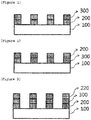
- Leitfähiger Strukturkörper, umfassend:ein Substrat (100);eine leitfähige Musterschicht (300), die auf dem Substrat (100) bereitgestellt ist; undeine Verdunkelungsmusterschicht (200), die auf wenigstens einer Oberfläche der leitfähigen Musterschicht (300) bereitgestellt ist,wobei die Verdunkelungsmusterschicht (200) ein Material auf Kupfer-Mangan-Basis, dargestellt durch CuaMnbOcNd, einschließt,wobei in dem Material auf Kupfer-Mangan-Basisb ein Massenverhältnis von Mn zu dem Material auf Kupfer-Mangan-Basis ist und 0,01 oder mehr und 0,5 oder weniger ist,c ein Massenverhältnis von O zu dem Material auf Kupfer-Mangan-Basis ist und 0,05 oder mehr und 0,6 oder weniger ist,d ein Massenverhältnis von N zu dem Material auf Kupfer-Mangan-Basis ist und 0 oder mehr und 0,15 oder weniger ist, unda ein Massenverhältnis von Cu zu dem Material auf Kupfer-Mangan-Basis ist und ein verbleibender Wert zu einer Summe der Massenverhältnisse der Komponenten, die andere sind als Cu, ist,wobei in dem Material auf Kupfer-Mangan-Basis c + d 0,15 oder mehr und 0,6 oder weniger ist.
- Leitfähiger Strukturkörper nach Anspruch 1, wobei in dem Material auf Kupfer-Mangan-Basis d 0 ist und c 0,25 oder mehr und 0,6 oder weniger ist.
- Leitfähiger Strukturkörper nach Anspruch 2, wobei die leitfähige Musterschicht zwischen dem Substrat und der Verdunkelungsmusterschicht bereitgestellt ist, und wobei das Totalreflexionsvermögen auf einer Oberfläche des Substrats gemessen wird, auf der das leitfähige Muster bereitgestellt ist.
- Leitfähiger Strukturkörper nach Anspruch 2, wobei die Verdunkelungsmusterschicht zwischen dem Substrat und der leitfähigen Musterschicht bereitgestellt ist, und wobei das Gesamtreflexionsvermögen auf einer gegenüberliegenden Oberfläche der Oberfläche des Substrats gemessen wird, auf der das leitfähige Muster bereitgestellt ist.
- Leitfähiger Strukturkörper nach Anspruch 1, wobei eine Dicke der Verdunkelungsmusterschicht 20 nm oder mehr und 100 nm oder weniger ist.
- Leitfähiger Strukturkörper nach Anspruch 1, wobei eine Dicke der leitfähigen Musterschicht 0,01 µm oder mehr und 10 µm oder weniger ist.
- Leitfähiger Strukturkörper nach Anspruch 1, wobei die leitfähige Musterschicht ein oder mehrere Materialien einschließt, die ausgewählt sind aus der Gruppe bestehend aus einem Metall, einer Metalllegierung, Metalloxid und Metallnitrid, und
die Materialien spezifische Widerstände von 1 x 10⁶ Ω · cm oder mehr und 30 x 106 Ω · cm oder weniger aufweisen. - Leitfähiger Strukturkörper nach Anspruch 1, wobei eine Linienbreite eines Musters der leitfähigen Musterschicht 10 µm oder weniger ist.
- Touchscreenpanel, umfassend:
den leitfähigen Strukturkörper nach einem der Ansprüche 1 bis 8. - Displayvorrichtung, umfassend:
den leitfähigen Strukturkörper nach einem der Ansprüche 1 bis 8. - Solarbatterie, umfassend:
den leitfähigen Strukturkörper nach einem der Ansprüche 1 bis 8. - Verfahren zum Herstellen eines leitfähigen Strukturkörpers, umfassend:Herstellen eines Substrats (100);Bilden einer leitfähigen Musterschicht (300) auf dem Substrat (100); undBilden einer Verdunkelungsmusterschicht (200) auf einer oberen Oberfläche, einer unteren Oberfläche oder der oberen Oberfläche und der unteren Oberfläche der leitfähigen Musterschicht (300),wobei die Verdunkelungsmusterschicht (200) ein Material auf Kupfer-Mangan-Basis, dargestellt durch CuaMnbOcNd, einschließt,wobei in dem Material auf Kupfer-Mangan-Basisb ein Massenverhältnis von Mn zu dem Material auf Kupfer-Mangan-Basis ist und 0,01 oder mehr und 0,5 oder weniger ist,c ein Massenverhältnis von O zu dem Material auf Kupfer-Mangan-Basis ist und 0,05 oder mehr und 0,6 oder weniger ist,d ein Massenverhältnis von N zu dem Material auf Kupfer-Mangan-Basis ist und 0 oder mehr und 0,15 oder weniger ist, unda ein Massenverhältnis von Cu zu dem Material auf Kupfer-Mangan-Basis ist und ein restlicher Wert zu einer Summe der Massenverhältnisse der anderen Komponenten als Cu ist,wobei in dem Material auf Kupfer-Mangan-Basis c + d 0,15 oder mehr und 0,6 oder weniger ist.
- Verfahren nach Anspruch 12, wobei das Bilden der leitfähigen Musterschicht ein Bilden einer leitfähigen Schicht auf dem Substrat einschließt,
wobei das Bilden der Verdunkelungsmusterschicht ein Bilden einer Verdunkelungsschicht auf einer oberen Oberfläche, einer unteren Oberfläche oder der oberen Oberfläche und der unteren Oberfläche der leitfähigen Schicht einschließt, und
die leitfähige Musterschicht und die Verdunkelungsmusterschicht durch simultanes Bemustern der leitfähigen Schicht und der Verdunkelungsschicht gebildet werden. - Verfahren nach Anspruch 13, wobei bei dem simultanen Bemustern ein Chargenätzen durch Verwendung eines Ätzmittels durchgeführt wird.
Applications Claiming Priority (2)
| Application Number | Priority Date | Filing Date | Title |
|---|---|---|---|
| KR20130133201 | 2013-11-04 | ||
| PCT/KR2014/010526 WO2015065162A1 (ko) | 2013-11-04 | 2014-11-04 | 전도성 구조체 및 이의 제조방법 |
Publications (3)
| Publication Number | Publication Date |
|---|---|
| EP2937766A1 EP2937766A1 (de) | 2015-10-28 |
| EP2937766A4 EP2937766A4 (de) | 2016-10-19 |
| EP2937766B1 true EP2937766B1 (de) | 2018-07-25 |
Family
ID=53004655
Family Applications (1)
| Application Number | Title | Priority Date | Filing Date |
|---|---|---|---|
| EP14857911.3A Active EP2937766B1 (de) | 2013-11-04 | 2014-11-04 | Leitfähige struktur und herstellungsverfahren dafür |
Country Status (6)
| Country | Link |
|---|---|
| US (1) | US9706653B2 (de) |
| EP (1) | EP2937766B1 (de) |
| KR (1) | KR101648636B1 (de) |
| CN (1) | CN105144045B (de) |
| TW (1) | TWI537989B (de) |
| WO (1) | WO2015065162A1 (de) |
Families Citing this family (10)
| Publication number | Priority date | Publication date | Assignee | Title |
|---|---|---|---|---|
| WO2015119437A1 (ko) * | 2014-02-05 | 2015-08-13 | 박철 | 전자기기용 투명커버 |
| WO2016072274A1 (ja) * | 2014-11-05 | 2016-05-12 | 日本写真印刷株式会社 | 電気配線部材の製造方法、および電気配線部材 |
| KR101987263B1 (ko) * | 2015-08-13 | 2019-06-10 | 주식회사 엘지화학 | 전도성 구조체 및 이의 제조방법 |
| WO2017099476A1 (ko) * | 2015-12-07 | 2017-06-15 | 주식회사 엘지화학 | 전도성 구조체, 이의 제조방법 및 전도성 구조체를 포함하는 전극 |
| KR102143261B1 (ko) * | 2016-04-01 | 2020-08-10 | 주식회사 엘지화학 | 잉크 조성물, 이로 제조된 경화 패턴, 이를 포함하는 발열체 및 이의 제조방법 |
| KR101929281B1 (ko) | 2016-05-19 | 2019-03-15 | 삼성디스플레이 주식회사 | 전자 장치 |
| KR102556838B1 (ko) * | 2016-06-01 | 2023-07-19 | 삼성디스플레이 주식회사 | 터치 패널, 이를 포함하는 전자 장치, 및 터치 패널 제조 방법 |
| JP6597487B2 (ja) * | 2016-06-15 | 2019-10-30 | 住友金属鉱山株式会社 | 電極基板フィルム及びその製造方法 |
| CN106648201B (zh) * | 2016-09-30 | 2019-07-19 | 业成科技(成都)有限公司 | 黑化金属网格结构及其制造方法 |
| KR20180078423A (ko) * | 2016-12-29 | 2018-07-10 | 삼성디스플레이 주식회사 | 표시 장치 및 이의 제조 방법 |
Family Cites Families (12)
| Publication number | Priority date | Publication date | Assignee | Title |
|---|---|---|---|---|
| JP4668438B2 (ja) | 2001-03-08 | 2011-04-13 | 住友ゴム工業株式会社 | 電磁波シールド板及びその製造方法 |
| JP4837297B2 (ja) | 2005-03-09 | 2011-12-14 | 富士フイルム株式会社 | 遮光画像付き基板及び遮光画像の形成方法、転写材料、カラーフィルター、並びに表示装置 |
| JP4867261B2 (ja) * | 2005-09-30 | 2012-02-01 | 大日本印刷株式会社 | 電磁波遮蔽シート |
| US7807296B2 (en) * | 2006-08-23 | 2010-10-05 | Roval, Inc. | Copper-manganese mixed oxide cathode material for use in alkaline cells having high capacity |
| KR101642511B1 (ko) | 2008-07-14 | 2016-07-25 | 주식회사 엘지화학 | 도전성 적층체 및 이의 제조방법 |
| WO2011070801A1 (ja) * | 2009-12-10 | 2011-06-16 | 凸版印刷株式会社 | 導電性基板およびその製造方法ならびにタッチパネル |
| TWI518739B (zh) * | 2011-10-27 | 2016-01-21 | 遠東新世紀股份有限公司 | 製造導電基材的方法 |
| JP5647864B2 (ja) | 2010-11-05 | 2015-01-07 | 富士フイルム株式会社 | タッチパネル |
| KR101221722B1 (ko) * | 2011-03-04 | 2013-01-11 | 주식회사 엘지화학 | 전도성 구조체 및 이의 제조방법 |
| KR20120138287A (ko) * | 2011-06-14 | 2012-12-26 | 삼성전기주식회사 | 터치패널 및 그 제조방법 |
| KR101244112B1 (ko) * | 2011-07-21 | 2013-03-18 | 주식회사 탑 엔지니어링 | 태양전지용 광흡수층 제조방법, 이를 포함하는 태양전지 및 이의 제조방법 |
| TWI506752B (zh) | 2012-04-18 | 2015-11-01 | Lg Chemical Ltd | 導電結構體及其製備方法 |
-
2014
- 2014-11-04 CN CN201480010016.9A patent/CN105144045B/zh active Active
- 2014-11-04 US US14/766,085 patent/US9706653B2/en active Active
- 2014-11-04 TW TW103138214A patent/TWI537989B/zh active
- 2014-11-04 EP EP14857911.3A patent/EP2937766B1/de active Active
- 2014-11-04 WO PCT/KR2014/010526 patent/WO2015065162A1/ko active Application Filing
- 2014-11-04 KR KR1020140152406A patent/KR101648636B1/ko active IP Right Grant
Non-Patent Citations (1)
| Title |
|---|
| None * |
Also Published As
| Publication number | Publication date |
|---|---|
| TW201528292A (zh) | 2015-07-16 |
| EP2937766A1 (de) | 2015-10-28 |
| US9706653B2 (en) | 2017-07-11 |
| KR101648636B1 (ko) | 2016-08-16 |
| EP2937766A4 (de) | 2016-10-19 |
| CN105144045A (zh) | 2015-12-09 |
| KR20150051915A (ko) | 2015-05-13 |
| US20150373844A1 (en) | 2015-12-24 |
| TWI537989B (zh) | 2016-06-11 |
| WO2015065162A1 (ko) | 2015-05-07 |
| CN105144045B (zh) | 2017-10-31 |
Similar Documents
| Publication | Publication Date | Title |
|---|---|---|
| EP2937766B1 (de) | Leitfähige struktur und herstellungsverfahren dafür | |
| EP2747093B1 (de) | Leitfähige struktur und herstellungsverfahren dafür | |
| US9766652B2 (en) | Conductive structure and method for manufacturing same | |
| KR101656581B1 (ko) | 전도성 구조체 및 이의 제조방법 | |
| EP2682949B1 (de) | Elektrisch leitfähige struktur und herstellungsverfahren dafür | |
| CN104584143B (zh) | 导电结构和制造该导电结构的方法 | |
| KR101987263B1 (ko) | 전도성 구조체 및 이의 제조방법 | |
| KR101849449B1 (ko) | 전도성 구조체 및 이의 제조방법 | |
| KR101980728B1 (ko) | 전도성 구조체, 이의 제조방법, 이를 포함하는 터치패널 및 이를 포함하는 디스플레이 장치 | |
| KR102100534B1 (ko) | 전도성 구조체 및 이의 제조방법 | |
| KR20150134835A (ko) | 전도성 구조체 및 이의 제조방법 | |
| KR20150134837A (ko) | 전도성 구조체 및 이의 제조방법 |
Legal Events
| Date | Code | Title | Description |
|---|---|---|---|
| PUAI | Public reference made under article 153(3) epc to a published international application that has entered the european phase |
Free format text: ORIGINAL CODE: 0009012 |
|
| 17P | Request for examination filed |
Effective date: 20150722 |
|
| AK | Designated contracting states |
Kind code of ref document: A1 Designated state(s): AL AT BE BG CH CY CZ DE DK EE ES FI FR GB GR HR HU IE IS IT LI LT LU LV MC MK MT NL NO PL PT RO RS SE SI SK SM TR |
|
| AX | Request for extension of the european patent |
Extension state: BA ME |
|
| A4 | Supplementary search report drawn up and despatched |
Effective date: 20160921 |
|
| RIC1 | Information provided on ipc code assigned before grant |
Ipc: G06F 3/041 20060101AFI20160915BHEP Ipc: G06F 3/044 20060101ALI20160915BHEP |
|
| DAX | Request for extension of the european patent (deleted) | ||
| GRAP | Despatch of communication of intention to grant a patent |
Free format text: ORIGINAL CODE: EPIDOSNIGR1 |
|
| RIC1 | Information provided on ipc code assigned before grant |
Ipc: H01L 31/0224 20060101ALI20180226BHEP Ipc: G06F 3/041 20060101AFI20180226BHEP Ipc: G06F 3/044 20060101ALI20180226BHEP |
|
| INTG | Intention to grant announced |
Effective date: 20180328 |
|
| GRAS | Grant fee paid |
Free format text: ORIGINAL CODE: EPIDOSNIGR3 |
|
| GRAA | (expected) grant |
Free format text: ORIGINAL CODE: 0009210 |
|
| AK | Designated contracting states |
Kind code of ref document: B1 Designated state(s): AL AT BE BG CH CY CZ DE DK EE ES FI FR GB GR HR HU IE IS IT LI LT LU LV MC MK MT NL NO PL PT RO RS SE SI SK SM TR |
|
| REG | Reference to a national code |
Ref country code: GB Ref legal event code: FG4D |
|
| REG | Reference to a national code |
Ref country code: CH Ref legal event code: EP |
|
| REG | Reference to a national code |
Ref country code: AT Ref legal event code: REF Ref document number: 1022454 Country of ref document: AT Kind code of ref document: T Effective date: 20180815 |
|
| REG | Reference to a national code |
Ref country code: IE Ref legal event code: FG4D |
|
| REG | Reference to a national code |
Ref country code: DE Ref legal event code: R096 Ref document number: 602014029339 Country of ref document: DE |
|
| REG | Reference to a national code |
Ref country code: FR Ref legal event code: PLFP Year of fee payment: 5 |
|
| REG | Reference to a national code |
Ref country code: NL Ref legal event code: MP Effective date: 20180725 |
|
| REG | Reference to a national code |
Ref country code: LT Ref legal event code: MG4D |
|
| PG25 | Lapsed in a contracting state [announced via postgrant information from national office to epo] |
Ref country code: NL Free format text: LAPSE BECAUSE OF FAILURE TO SUBMIT A TRANSLATION OF THE DESCRIPTION OR TO PAY THE FEE WITHIN THE PRESCRIBED TIME-LIMIT Effective date: 20180725 |
|
| REG | Reference to a national code |
Ref country code: AT Ref legal event code: MK05 Ref document number: 1022454 Country of ref document: AT Kind code of ref document: T Effective date: 20180725 |
|
| PG25 | Lapsed in a contracting state [announced via postgrant information from national office to epo] |
Ref country code: GR Free format text: LAPSE BECAUSE OF FAILURE TO SUBMIT A TRANSLATION OF THE DESCRIPTION OR TO PAY THE FEE WITHIN THE PRESCRIBED TIME-LIMIT Effective date: 20181026 Ref country code: NO Free format text: LAPSE BECAUSE OF FAILURE TO SUBMIT A TRANSLATION OF THE DESCRIPTION OR TO PAY THE FEE WITHIN THE PRESCRIBED TIME-LIMIT Effective date: 20181025 Ref country code: SE Free format text: LAPSE BECAUSE OF FAILURE TO SUBMIT A TRANSLATION OF THE DESCRIPTION OR TO PAY THE FEE WITHIN THE PRESCRIBED TIME-LIMIT Effective date: 20180725 Ref country code: BG Free format text: LAPSE BECAUSE OF FAILURE TO SUBMIT A TRANSLATION OF THE DESCRIPTION OR TO PAY THE FEE WITHIN THE PRESCRIBED TIME-LIMIT Effective date: 20181025 Ref country code: LT Free format text: LAPSE BECAUSE OF FAILURE TO SUBMIT A TRANSLATION OF THE DESCRIPTION OR TO PAY THE FEE WITHIN THE PRESCRIBED TIME-LIMIT Effective date: 20180725 Ref country code: PL Free format text: LAPSE BECAUSE OF FAILURE TO SUBMIT A TRANSLATION OF THE DESCRIPTION OR TO PAY THE FEE WITHIN THE PRESCRIBED TIME-LIMIT Effective date: 20180725 Ref country code: FI Free format text: LAPSE BECAUSE OF FAILURE TO SUBMIT A TRANSLATION OF THE DESCRIPTION OR TO PAY THE FEE WITHIN THE PRESCRIBED TIME-LIMIT Effective date: 20180725 Ref country code: RS Free format text: LAPSE BECAUSE OF FAILURE TO SUBMIT A TRANSLATION OF THE DESCRIPTION OR TO PAY THE FEE WITHIN THE PRESCRIBED TIME-LIMIT Effective date: 20180725 Ref country code: IS Free format text: LAPSE BECAUSE OF FAILURE TO SUBMIT A TRANSLATION OF THE DESCRIPTION OR TO PAY THE FEE WITHIN THE PRESCRIBED TIME-LIMIT Effective date: 20181125 Ref country code: AT Free format text: LAPSE BECAUSE OF FAILURE TO SUBMIT A TRANSLATION OF THE DESCRIPTION OR TO PAY THE FEE WITHIN THE PRESCRIBED TIME-LIMIT Effective date: 20180725 |
|
| PG25 | Lapsed in a contracting state [announced via postgrant information from national office to epo] |
Ref country code: HR Free format text: LAPSE BECAUSE OF FAILURE TO SUBMIT A TRANSLATION OF THE DESCRIPTION OR TO PAY THE FEE WITHIN THE PRESCRIBED TIME-LIMIT Effective date: 20180725 Ref country code: LV Free format text: LAPSE BECAUSE OF FAILURE TO SUBMIT A TRANSLATION OF THE DESCRIPTION OR TO PAY THE FEE WITHIN THE PRESCRIBED TIME-LIMIT Effective date: 20180725 Ref country code: AL Free format text: LAPSE BECAUSE OF FAILURE TO SUBMIT A TRANSLATION OF THE DESCRIPTION OR TO PAY THE FEE WITHIN THE PRESCRIBED TIME-LIMIT Effective date: 20180725 |
|
| REG | Reference to a national code |
Ref country code: DE Ref legal event code: R097 Ref document number: 602014029339 Country of ref document: DE |
|
| PG25 | Lapsed in a contracting state [announced via postgrant information from national office to epo] |
Ref country code: RO Free format text: LAPSE BECAUSE OF FAILURE TO SUBMIT A TRANSLATION OF THE DESCRIPTION OR TO PAY THE FEE WITHIN THE PRESCRIBED TIME-LIMIT Effective date: 20180725 Ref country code: EE Free format text: LAPSE BECAUSE OF FAILURE TO SUBMIT A TRANSLATION OF THE DESCRIPTION OR TO PAY THE FEE WITHIN THE PRESCRIBED TIME-LIMIT Effective date: 20180725 Ref country code: IT Free format text: LAPSE BECAUSE OF FAILURE TO SUBMIT A TRANSLATION OF THE DESCRIPTION OR TO PAY THE FEE WITHIN THE PRESCRIBED TIME-LIMIT Effective date: 20180725 Ref country code: ES Free format text: LAPSE BECAUSE OF FAILURE TO SUBMIT A TRANSLATION OF THE DESCRIPTION OR TO PAY THE FEE WITHIN THE PRESCRIBED TIME-LIMIT Effective date: 20180725 Ref country code: CZ Free format text: LAPSE BECAUSE OF FAILURE TO SUBMIT A TRANSLATION OF THE DESCRIPTION OR TO PAY THE FEE WITHIN THE PRESCRIBED TIME-LIMIT Effective date: 20180725 |
|
| PG25 | Lapsed in a contracting state [announced via postgrant information from national office to epo] |
Ref country code: SK Free format text: LAPSE BECAUSE OF FAILURE TO SUBMIT A TRANSLATION OF THE DESCRIPTION OR TO PAY THE FEE WITHIN THE PRESCRIBED TIME-LIMIT Effective date: 20180725 Ref country code: SM Free format text: LAPSE BECAUSE OF FAILURE TO SUBMIT A TRANSLATION OF THE DESCRIPTION OR TO PAY THE FEE WITHIN THE PRESCRIBED TIME-LIMIT Effective date: 20180725 Ref country code: DK Free format text: LAPSE BECAUSE OF FAILURE TO SUBMIT A TRANSLATION OF THE DESCRIPTION OR TO PAY THE FEE WITHIN THE PRESCRIBED TIME-LIMIT Effective date: 20180725 |
|
| PLBE | No opposition filed within time limit |
Free format text: ORIGINAL CODE: 0009261 |
|
| STAA | Information on the status of an ep patent application or granted ep patent |
Free format text: STATUS: NO OPPOSITION FILED WITHIN TIME LIMIT |
|
| REG | Reference to a national code |
Ref country code: CH Ref legal event code: PL |
|
| 26N | No opposition filed |
Effective date: 20190426 |
|
| PG25 | Lapsed in a contracting state [announced via postgrant information from national office to epo] |
Ref country code: MC Free format text: LAPSE BECAUSE OF FAILURE TO SUBMIT A TRANSLATION OF THE DESCRIPTION OR TO PAY THE FEE WITHIN THE PRESCRIBED TIME-LIMIT Effective date: 20180725 Ref country code: LU Free format text: LAPSE BECAUSE OF NON-PAYMENT OF DUE FEES Effective date: 20181104 |
|
| REG | Reference to a national code |
Ref country code: BE Ref legal event code: MM Effective date: 20181130 |
|
| REG | Reference to a national code |
Ref country code: IE Ref legal event code: MM4A |
|
| PG25 | Lapsed in a contracting state [announced via postgrant information from national office to epo] |
Ref country code: SI Free format text: LAPSE BECAUSE OF FAILURE TO SUBMIT A TRANSLATION OF THE DESCRIPTION OR TO PAY THE FEE WITHIN THE PRESCRIBED TIME-LIMIT Effective date: 20180725 Ref country code: LI Free format text: LAPSE BECAUSE OF NON-PAYMENT OF DUE FEES Effective date: 20181130 Ref country code: CH Free format text: LAPSE BECAUSE OF NON-PAYMENT OF DUE FEES Effective date: 20181130 |
|
| PG25 | Lapsed in a contracting state [announced via postgrant information from national office to epo] |
Ref country code: IE Free format text: LAPSE BECAUSE OF NON-PAYMENT OF DUE FEES Effective date: 20181104 |
|
| PG25 | Lapsed in a contracting state [announced via postgrant information from national office to epo] |
Ref country code: BE Free format text: LAPSE BECAUSE OF NON-PAYMENT OF DUE FEES Effective date: 20181130 |
|
| PG25 | Lapsed in a contracting state [announced via postgrant information from national office to epo] |
Ref country code: MT Free format text: LAPSE BECAUSE OF NON-PAYMENT OF DUE FEES Effective date: 20181104 |
|
| PG25 | Lapsed in a contracting state [announced via postgrant information from national office to epo] |
Ref country code: TR Free format text: LAPSE BECAUSE OF FAILURE TO SUBMIT A TRANSLATION OF THE DESCRIPTION OR TO PAY THE FEE WITHIN THE PRESCRIBED TIME-LIMIT Effective date: 20180725 |
|
| PG25 | Lapsed in a contracting state [announced via postgrant information from national office to epo] |
Ref country code: PT Free format text: LAPSE BECAUSE OF FAILURE TO SUBMIT A TRANSLATION OF THE DESCRIPTION OR TO PAY THE FEE WITHIN THE PRESCRIBED TIME-LIMIT Effective date: 20180725 |
|
| PG25 | Lapsed in a contracting state [announced via postgrant information from national office to epo] |
Ref country code: CY Free format text: LAPSE BECAUSE OF FAILURE TO SUBMIT A TRANSLATION OF THE DESCRIPTION OR TO PAY THE FEE WITHIN THE PRESCRIBED TIME-LIMIT Effective date: 20180725 Ref country code: HU Free format text: LAPSE BECAUSE OF FAILURE TO SUBMIT A TRANSLATION OF THE DESCRIPTION OR TO PAY THE FEE WITHIN THE PRESCRIBED TIME-LIMIT; INVALID AB INITIO Effective date: 20141104 Ref country code: MK Free format text: LAPSE BECAUSE OF NON-PAYMENT OF DUE FEES Effective date: 20180725 |
|
| PGFP | Annual fee paid to national office [announced via postgrant information from national office to epo] |
Ref country code: GB Payment date: 20231023 Year of fee payment: 10 |
|
| PGFP | Annual fee paid to national office [announced via postgrant information from national office to epo] |
Ref country code: FR Payment date: 20231024 Year of fee payment: 10 Ref country code: DE Payment date: 20231023 Year of fee payment: 10 |