EP2936679B1 - Amplificateurs de puissance multibande multimode - Google Patents
Amplificateurs de puissance multibande multimode Download PDFInfo
- Publication number
- EP2936679B1 EP2936679B1 EP13821320.2A EP13821320A EP2936679B1 EP 2936679 B1 EP2936679 B1 EP 2936679B1 EP 13821320 A EP13821320 A EP 13821320A EP 2936679 B1 EP2936679 B1 EP 2936679B1
- Authority
- EP
- European Patent Office
- Prior art keywords
- amplifier
- transformer
- signal
- band
- mode
- Prior art date
- Legal status (The legal status is an assumption and is not a legal conclusion. Google has not performed a legal analysis and makes no representation as to the accuracy of the status listed.)
- Active
Links
- 238000004804 winding Methods 0.000 claims description 56
- 238000000034 method Methods 0.000 claims description 27
- 239000003990 capacitor Substances 0.000 claims description 22
- 230000008878 coupling Effects 0.000 claims description 14
- 238000010168 coupling process Methods 0.000 claims description 14
- 238000005859 coupling reaction Methods 0.000 claims description 14
- 101100337798 Drosophila melanogaster grnd gene Proteins 0.000 description 15
- 238000004891 communication Methods 0.000 description 7
- 230000008569 process Effects 0.000 description 7
- 238000005516 engineering process Methods 0.000 description 6
- 238000003780 insertion Methods 0.000 description 5
- 230000037431 insertion Effects 0.000 description 5
- 241001125929 Trisopterus luscus Species 0.000 description 4
- 238000013461 design Methods 0.000 description 4
- 230000006870 function Effects 0.000 description 4
- 238000010586 diagram Methods 0.000 description 3
- 230000003287 optical effect Effects 0.000 description 3
- 239000000835 fiber Substances 0.000 description 2
- 230000001939 inductive effect Effects 0.000 description 2
- 230000007774 longterm Effects 0.000 description 2
- 239000002245 particle Substances 0.000 description 2
- 238000012545 processing Methods 0.000 description 2
- 230000001413 cellular effect Effects 0.000 description 1
- 230000000295 complement effect Effects 0.000 description 1
- 238000004590 computer program Methods 0.000 description 1
- 230000003750 conditioning effect Effects 0.000 description 1
- 230000003247 decreasing effect Effects 0.000 description 1
- 230000009977 dual effect Effects 0.000 description 1
- 238000010295 mobile communication Methods 0.000 description 1
- 238000012986 modification Methods 0.000 description 1
- 230000004048 modification Effects 0.000 description 1
- 230000003071 parasitic effect Effects 0.000 description 1
- 230000009467 reduction Effects 0.000 description 1
- 239000000758 substrate Substances 0.000 description 1
- 238000012546 transfer Methods 0.000 description 1
- 230000009466 transformation Effects 0.000 description 1
Images


Classifications
-
- H—ELECTRICITY
- H04—ELECTRIC COMMUNICATION TECHNIQUE
- H04B—TRANSMISSION
- H04B1/00—Details of transmission systems, not covered by a single one of groups H04B3/00 - H04B13/00; Details of transmission systems not characterised by the medium used for transmission
- H04B1/02—Transmitters
- H04B1/04—Circuits
- H04B1/0458—Arrangements for matching and coupling between power amplifier and antenna or between amplifying stages
-
- H—ELECTRICITY
- H03—ELECTRONIC CIRCUITRY
- H03F—AMPLIFIERS
- H03F1/00—Details of amplifiers with only discharge tubes, only semiconductor devices or only unspecified devices as amplifying elements
- H03F1/02—Modifications of amplifiers to raise the efficiency, e.g. gliding Class A stages, use of an auxiliary oscillation
- H03F1/0205—Modifications of amplifiers to raise the efficiency, e.g. gliding Class A stages, use of an auxiliary oscillation in transistor amplifiers
- H03F1/0277—Selecting one or more amplifiers from a plurality of amplifiers
-
- H—ELECTRICITY
- H03—ELECTRONIC CIRCUITRY
- H03F—AMPLIFIERS
- H03F3/00—Amplifiers with only discharge tubes or only semiconductor devices as amplifying elements
- H03F3/72—Gated amplifiers, i.e. amplifiers which are rendered operative or inoperative by means of a control signal
-
- H—ELECTRICITY
- H04—ELECTRIC COMMUNICATION TECHNIQUE
- H04B—TRANSMISSION
- H04B1/00—Details of transmission systems, not covered by a single one of groups H04B3/00 - H04B13/00; Details of transmission systems not characterised by the medium used for transmission
- H04B1/02—Transmitters
- H04B1/04—Circuits
- H04B1/0483—Transmitters with multiple parallel paths
-
- H—ELECTRICITY
- H03—ELECTRONIC CIRCUITRY
- H03F—AMPLIFIERS
- H03F2203/00—Indexing scheme relating to amplifiers with only discharge tubes or only semiconductor devices as amplifying elements covered by H03F3/00
- H03F2203/72—Indexing scheme relating to gated amplifiers, i.e. amplifiers which are rendered operative or inoperative by means of a control signal
- H03F2203/7239—Indexing scheme relating to gated amplifiers, i.e. amplifiers which are rendered operative or inoperative by means of a control signal the gated amplifier being switched on or off by putting into parallel or not, by choosing between amplifiers and shunting lines by one or more switch(es)
-
- H—ELECTRICITY
- H03—ELECTRONIC CIRCUITRY
- H03H—IMPEDANCE NETWORKS, e.g. RESONANT CIRCUITS; RESONATORS
- H03H7/00—Multiple-port networks comprising only passive electrical elements as network components
- H03H7/38—Impedance-matching networks
Landscapes
- Engineering & Computer Science (AREA)
- Computer Networks & Wireless Communication (AREA)
- Signal Processing (AREA)
- Power Engineering (AREA)
- Amplifiers (AREA)
Claims (15)
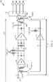
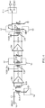
- Appareil (200) comprenant :une voie de transmission comprenant un premier amplificateur (204) et un deuxième amplificateur (206) ; etun transformateur (T2) comprenant un enroulement primaire (T2P) et une enroulement secondaire (T2S), couplé entre la sortie du premier amplificateur (204) et l'entrée du deuxième amplificateur (206), et configuré de manière commutable pour, dans un premier mode, coupler de façon différentielle le premier amplificateur (204) en série avec le deuxième amplificateur (206) et pour, dans un deuxième mode, coupler de façon asymétrique le premier amplificateur (204) pour contourner le deuxième amplificateur (206) via une extrémité de l'enroulement secondaire (T2S) du transformateur (T2) et coupler une autre extrémité de l'enroulement secondaire (T2S) à la masse.
- Appareil (200) selon la revendication 1, comprenant en outre une autre voie de transmission comprenant un troisième amplificateur (212) pour fonctionner dans un troisième mode.
- Appareil (200) selon la revendication 2, comprenant en outre :un premier commutateur (S9) pour coupler la voie de transmission ou l'autre voie de transmission à l'une d'une première borne de bande et d'une deuxième borne de bande ; etun second commutateur (S10) pour coupler la voie de transmission ou l'autre voie de transmission à l'une d'une troisième borne de bande et d'une quatrième borne de bande.
- Appareil (200) selon la revendication 2, dans lequel le premier mode comprend un mode haute puissance, le deuxième mode comprenant un mode puissance moyenne, et le troisième mode comprenant un mode basse puissance.
- Appareil (200) selon la revendication 1, dans lequel la voie de transmission comprend :
un deuxième transformateur (T1) pour recevoir un signal d'entrée asymétrique et acheminer un signal de sortie différentiel vers le premier amplificateur (204), comprenant en outre un troisième transformateur (T3) pour recevoir un signal d'entrée différentiel acheminé depuis le deuxième amplificateur (206) et acheminer un signal asymétrique vers une sortie. - Appareil (200) selon la revendication 1, dans lequel le transformateur (T2) est destiné à recevoir le signal de sortie et est configuré de manière commutable pour acheminer un signal différentiel vers le deuxième amplificateur dans le premier mode ou acheminer un signal asymétrique pour contourner le deuxième amplificateur (206) dans le deuxième mode.
- Appareil (200) selon la revendication 1, comprenant en outre un premier commutateur pour coupler à une sortie du premier amplificateur ou du deuxième amplificateur et pour sélectionner une première bande ou une deuxième bande, et un second commutateur, différent, pour coupler à une sortie du premier amplificateur ou du deuxième amplificateur et pour sélectionner une troisième bande ou une quatrième bande.
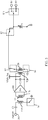
- Procédé (700) comprenant :l'amplification (702) d'un signal avec au moins un premier amplificateur et un deuxième amplificateur et un transformateur (T2) couplé entre la sortie du premier amplificateur et l'entrée du deuxième amplificateur dans chacun d'une pluralité de modes de fonctionnement, le transformateur (T2) couplant de façon différentielle un premier amplificateur (204) en série avec un deuxième amplificateur (206) dans un premier mode de fonctionnement et le transformateur (T2) couplant de façon asymétrique le premier amplificateur (204) pour contourner le deuxième amplificateur (206) via une extrémité de l'enroulement secondaire (T2S) du transformateur (T2) et couplant une autre extrémité de l'enroulement secondaire (T2S) à la masse dans un deuxième mode de fonctionnement ; etl'acheminement (704) du signal amplifié vers une première voie de sortie si l'une d'une première pluralité de bornes de bande est sélectionnée ; etl'acheminement (706) du signal amplifié vers une seconde voie de sortie si l'un d'une seconde pluralité de bornes de bande est sélectionnée.
- Procédé (700) selon la revendication 8, dans lequel l'amplification comprend :l'amplification du signal avec le premier amplificateur (204) et le second amplificateur (206) dans un premier mode de fonctionnement ;l'amplification du signal avec le premier amplificateur dans un deuxième mode de fonctionnement ; etl'amplification du signal avec un troisième amplificateur (212) dans un troisième mode de fonctionnement.
- Procédé (700) selon la revendication 9, comprenant en outre la configuration commutable du transformateur (T2) pour acheminer un signal fourni par le premier amplificateur (204) vers le deuxième amplificateur (206) dans le premier mode de fonctionnement.
- Procédé (700) selon la revendication 9, comprenant en outre la configuration commutable du transformateur (T2) pour acheminer un signal fourni par le premier amplificateur (204) à l'un de la première voie de sortie et de la seconde voie de sortie dans le deuxième mode de fonctionnement.
- Procédé (700) selon la revendication 8, l'amplification comprenant :la conversion d'un signal asymétrique en un signal différentiel au niveau d'un deuxième transformateur (T1) ; etla conversion d'un signal différentiel amplifié en un signal asymétrique au niveau du transformateur (T2).
- Procédé (700) selon la revendication 8, comprenant en outre la fourniture du signal via l'un d'une pluralité de commutateurs sur la base d'une bande sélectionnée, la fourniture comprenant l'une parmi la fourniture du signal via un premier commutateur si l'une parmi une première bande et une deuxième bande est sélectionnée et la fourniture du signal via un second commutateur si l'une parmi une troisième bande et une quatrième bande est sélectionnée.
- Procédé (700) selon la revendication 8, comprenant en outre la fourniture d'une adaptation d'impédance à partir d'une sortie du premier amplificateur vers une entrée du deuxième amplificateur dans une mode haute puissance, dans lequel le premier amplificateur est un amplificateur de commande et le deuxième amplificateur est un amplificateur de puissance.
- Procédé (700) selon la revendication 8, dans lequel un condensateur est accordé pour fournir au moins l'un parmi l'adaptation entre étages et l'adaptation de sortie pour le au moins un amplificateur.
Applications Claiming Priority (2)
| Application Number | Priority Date | Filing Date | Title |
|---|---|---|---|
| US13/720,851 US9160377B2 (en) | 2012-12-19 | 2012-12-19 | Multi-mode multi-band power amplifiers |
| PCT/US2013/076749 WO2014100513A1 (fr) | 2012-12-19 | 2013-12-19 | Amplificateurs de puissance multibande multimode |
Publications (2)
| Publication Number | Publication Date |
|---|---|
| EP2936679A1 EP2936679A1 (fr) | 2015-10-28 |
| EP2936679B1 true EP2936679B1 (fr) | 2018-10-17 |
Family
ID=49956436
Family Applications (1)
| Application Number | Title | Priority Date | Filing Date |
|---|---|---|---|
| EP13821320.2A Active EP2936679B1 (fr) | 2012-12-19 | 2013-12-19 | Amplificateurs de puissance multibande multimode |
Country Status (5)
| Country | Link |
|---|---|
| US (1) | US9160377B2 (fr) |
| EP (1) | EP2936679B1 (fr) |
| JP (1) | JP6017704B2 (fr) |
| CN (1) | CN104854790B (fr) |
| WO (1) | WO2014100513A1 (fr) |
Families Citing this family (34)
| Publication number | Priority date | Publication date | Assignee | Title |
|---|---|---|---|---|
| US9444498B2 (en) * | 2012-12-03 | 2016-09-13 | Broadcom Corporation | Repartitioned transceiver using silicon-on-insulator |
| US9515615B2 (en) | 2013-02-20 | 2016-12-06 | Micro Mobio Corporation | World band radio frequency front end module, system and method thereof |
| US10643962B1 (en) | 2013-02-20 | 2020-05-05 | Micro Mobio Corporation | World band radio frequency front end module, system and method of power sensing thereof |
| US10027287B1 (en) | 2013-02-20 | 2018-07-17 | Micro Mobio Corporation | World band frequency front end module, system and method thereof |
| US9178555B2 (en) * | 2013-02-20 | 2015-11-03 | Micro Mobio Corporation | World band radio frequency front end module, system and method thereof |
| US9425835B2 (en) * | 2013-08-09 | 2016-08-23 | Broadcom Corporation | Transmitter with reduced counter-intermodulation |
| JP6291796B2 (ja) * | 2013-11-08 | 2018-03-14 | 株式会社ソシオネクスト | 増幅器 |
| US9595933B2 (en) * | 2013-12-30 | 2017-03-14 | Lansus Technologies Inc. | Power amplifier device and circuits |
| US9590569B2 (en) * | 2014-05-06 | 2017-03-07 | Skyworks Solutions, Inc. | Systems, circuits and methods related to low power efficiency improvement in multi-mode multi-band power amplifiers |
| US9356560B2 (en) * | 2014-08-01 | 2016-05-31 | Qualcomm Incorporated | Multi-mode integrated power amplifier |
| US9548767B2 (en) | 2014-11-04 | 2017-01-17 | Qualcomm Incorporated | Multi-band amplifier |
| KR102123600B1 (ko) | 2015-05-29 | 2020-06-15 | 삼성전기주식회사 | 프론트 엔드 회로 |
| US9543900B1 (en) | 2015-06-19 | 2017-01-10 | Qualcomm Incorporated | Switchable supply and tunable load impedance power amplifier |
| US10103754B2 (en) * | 2016-07-17 | 2018-10-16 | Skyworks Solutions, Inc. | Architectures and methods related to transmit signal routing with re-use of filters |
| US10177723B2 (en) | 2016-08-30 | 2019-01-08 | Qualcomm Incorporated | Reconfigurable power amplifier |
| US10256783B2 (en) * | 2016-11-29 | 2019-04-09 | Taiwan Semiconductor Manufacturing Co., Ltd. | Dual-mode RF transmission frontend |
| JP2018137566A (ja) * | 2017-02-21 | 2018-08-30 | 株式会社村田製作所 | 電力増幅回路 |
| US10230300B2 (en) * | 2017-04-25 | 2019-03-12 | Cirrus Logic, Inc. | Power converter predriver system with multiple power modes |
| US10110177B1 (en) * | 2017-07-28 | 2018-10-23 | Silicon Laboratories Inc. | Programmable impedance control for a transformer |
| US11476814B2 (en) * | 2018-01-23 | 2022-10-18 | Teknologian tukimuskeskus VTT Oy | Transformer based switches and systems for PALNA transceivers |
| US10333579B1 (en) * | 2018-04-12 | 2019-06-25 | Shenzhen GOODIX Technology Co., Ltd. | Multi-mode configurable transceiver with low voltage switches |
| CN109196783B (zh) * | 2018-04-12 | 2020-04-24 | 深圳市汇顶科技股份有限公司 | 具有低电压开关的多模式可配置的收发器及其配置方法 |
| WO2020036866A1 (fr) * | 2018-08-13 | 2020-02-20 | Skyworks Solutions, Inc. | Amplificateur de puissance push-pull commutable pour ligne de charge |
| WO2020068939A1 (fr) * | 2018-09-26 | 2020-04-02 | Skyworks Solutions, Inc. | Commutation de ligne de charge pour amplificateurs de puissance push-pull |
| JP7275624B2 (ja) * | 2019-02-13 | 2023-05-18 | 株式会社デンソー | 周波数帯域可変高周波増幅器 |
| RU2710292C1 (ru) * | 2019-05-22 | 2019-12-25 | федеральное государственное бюджетное образовательное учреждение высшего образования "Донской государственный технический университет" (ДГТУ | Низкочувствительный активный rc-фильтр второго порядка на основе двух мультидифференциальных операционных усилителей |
| RU2710852C1 (ru) * | 2019-05-23 | 2020-01-14 | федеральное государственное бюджетное образовательное учреждение высшего образования "Донской государственный технический университет" (ДГТУ) | Низкочувствительный arc-фильтр второго порядка на основе двух мультидифференциальных операционных усилителей |
| US11050387B2 (en) * | 2019-09-09 | 2021-06-29 | Texas Instruments Incorporated | Integrated circuit devices with parallel power amplifier output paths |
| RU2720559C1 (ru) * | 2019-11-22 | 2020-05-12 | федеральное государственное бюджетное образовательное учреждение высшего образования "Донской государственный технический университет" (ДГТУ) | Активный rc-фильтр нижних частот с одноэлементной перестройкой частоты полюса на дифференциальном и двух мультидифференциальных операционных усилителях |
| JP2022012549A (ja) | 2020-07-01 | 2022-01-17 | 株式会社村田製作所 | 電力増幅回路 |
| CN112398777B (zh) * | 2020-10-21 | 2023-02-03 | 中交航信(上海)科技有限公司 | 甚高频数据交换系统 |
| US11606109B2 (en) * | 2021-04-22 | 2023-03-14 | Texas Instruments Incorporated | Dynamically configurable transmitter power levels |
| US20230049925A1 (en) * | 2021-08-16 | 2023-02-16 | Qualcomm Incorporated | Multi-mode multi-port driver for transceiver interface |
| WO2023068079A1 (fr) * | 2021-10-22 | 2023-04-27 | 株式会社村田製作所 | Circuit haute-fréquence et dispositif de communication |
Family Cites Families (15)
| Publication number | Priority date | Publication date | Assignee | Title |
|---|---|---|---|---|
| JPH07115331A (ja) * | 1993-10-19 | 1995-05-02 | Mitsubishi Electric Corp | 増幅装置 |
| US6111459A (en) * | 1995-09-29 | 2000-08-29 | Matsushita Electric Industrial Co., Ltd. | Multi mode power amplifier and communication unit |
| JPH09148852A (ja) * | 1995-11-24 | 1997-06-06 | Matsushita Electric Ind Co Ltd | 送信出力可変装置 |
| JP3587346B2 (ja) * | 1998-08-07 | 2004-11-10 | 松下電器産業株式会社 | 無線通信装置および無線通信装置における送信電力制御方法 |
| US6625430B2 (en) * | 1998-12-15 | 2003-09-23 | Ericsson Inc. | Method and apparatus for attaining higher amplifier efficiencies at lower power levels |
| US8130043B2 (en) | 2003-09-25 | 2012-03-06 | Anadigics, Inc. | Multi-stage power amplifier with enhanced efficiency |
| DE10361660A1 (de) | 2003-12-30 | 2005-02-03 | Infineon Technologies Ag | Leistungsverstärkeranordnung und Verfahren zum Verstärken eines Signals |
| US8280325B2 (en) | 2006-06-23 | 2012-10-02 | Broadcom Corporation | Configurable transmitter |
| US7630693B2 (en) * | 2006-11-16 | 2009-12-08 | Freescale Semiconductor, Inc. | Transmitter with improved power efficiency |
| US7952433B2 (en) | 2008-11-25 | 2011-05-31 | Samsung Electro-Mechanics Company | Power amplifiers with discrete power control |
| US8068795B2 (en) * | 2009-03-24 | 2011-11-29 | Freescale Semiconductor, Inc. | RF multiband transmitter with balun |
| US8536950B2 (en) | 2009-08-03 | 2013-09-17 | Qualcomm Incorporated | Multi-stage impedance matching |
| US8149050B2 (en) * | 2009-11-13 | 2012-04-03 | Qualcomm, Incorporated | Cascaded amplifiers with transformer-based bypass mode |
| US7944296B1 (en) | 2010-03-12 | 2011-05-17 | Samsung Electro-Mechanics Company | Low power mode amplification with a transformer output matching and a virtual ground |
| JPWO2012098863A1 (ja) * | 2011-01-20 | 2014-06-09 | パナソニック株式会社 | 高周波電力増幅器 |
-
2012
- 2012-12-19 US US13/720,851 patent/US9160377B2/en active Active
-
2013
- 2013-12-19 EP EP13821320.2A patent/EP2936679B1/fr active Active
- 2013-12-19 JP JP2015549748A patent/JP6017704B2/ja active Active
- 2013-12-19 CN CN201380065958.2A patent/CN104854790B/zh active Active
- 2013-12-19 WO PCT/US2013/076749 patent/WO2014100513A1/fr active Application Filing
Non-Patent Citations (1)
| Title |
|---|
| None * |
Also Published As
| Publication number | Publication date |
|---|---|
| CN104854790A (zh) | 2015-08-19 |
| US9160377B2 (en) | 2015-10-13 |
| JP2016501503A (ja) | 2016-01-18 |
| WO2014100513A1 (fr) | 2014-06-26 |
| EP2936679A1 (fr) | 2015-10-28 |
| JP6017704B2 (ja) | 2016-11-02 |
| CN104854790B (zh) | 2017-06-30 |
| US20150050901A1 (en) | 2015-02-19 |
Similar Documents
| Publication | Publication Date | Title |
|---|---|---|
| EP2936679B1 (fr) | Amplificateurs de puissance multibande multimode | |
| EP2959578B1 (fr) | Amplificateurs équipés de sorties multiples et inductance de contre-réaction configurable | |
| EP3227999B1 (fr) | Amplificateur à bobines d'inductances à triple couplage | |
| US9166852B2 (en) | Low noise amplifiers with transformer-based signal splitting for carrier aggregation | |
| EP2949042B1 (fr) | Amplificateurs avec isolation améliorée | |
| CN102428648B (zh) | 用于功率放大器及其它电路的具有集成的阻抗匹配、功率组合及滤波的输出电路 | |
| US10177722B2 (en) | Carrier aggregation low-noise amplifier with tunable integrated power splitter | |
| US20150194944A1 (en) | Wideband matching network | |
| CN104067513A (zh) | 具有可调谐负载匹配的多模旁路激励放大器 | |
| CN105409116A (zh) | 具有可配置的相互耦合的源极退化电感器的放大器 | |
| US20180048293A1 (en) | Reconfigurable radio frequency (rf) bandstop / intermediate frequency (if) bandpass filter | |
| WO2018031198A1 (fr) | Amplificateur à faible bruit de bande passante à étages multiples | |
| US20210099140A1 (en) | Wide bandwidth radio frequency (rf) amplifier | |
| US20180175798A1 (en) | Area efficient architecture to combine outputs of parallel transmit signal paths | |
| US10122332B2 (en) | Low-noise amplifier with integrated wideband transformer-based power splitter | |
| US20170201408A1 (en) | Wireless receiver for carrier aggregation | |
| US20220302883A1 (en) | Wideband amplifier |
Legal Events
| Date | Code | Title | Description |
|---|---|---|---|
| PUAI | Public reference made under article 153(3) epc to a published international application that has entered the european phase |
Free format text: ORIGINAL CODE: 0009012 |
|
| 17P | Request for examination filed |
Effective date: 20150714 |
|
| AK | Designated contracting states |
Kind code of ref document: A1 Designated state(s): AL AT BE BG CH CY CZ DE DK EE ES FI FR GB GR HR HU IE IS IT LI LT LU LV MC MK MT NL NO PL PT RO RS SE SI SK SM TR |
|
| AX | Request for extension of the european patent |
Extension state: BA ME |
|
| DAX | Request for extension of the european patent (deleted) | ||
| REG | Reference to a national code |
Ref country code: DE Ref legal event code: R079 Ref document number: 602013045333 Country of ref document: DE Free format text: PREVIOUS MAIN CLASS: H03F0003720000 Ipc: H04B0001040000 |
|
| GRAP | Despatch of communication of intention to grant a patent |
Free format text: ORIGINAL CODE: EPIDOSNIGR1 |
|
| RIC1 | Information provided on ipc code assigned before grant |
Ipc: H03F 3/72 20060101ALI20180419BHEP Ipc: H04B 1/04 20060101AFI20180419BHEP Ipc: H03F 1/02 20060101ALI20180419BHEP Ipc: H03H 7/38 20060101ALI20180419BHEP |
|
| INTG | Intention to grant announced |
Effective date: 20180511 |
|
| GRAS | Grant fee paid |
Free format text: ORIGINAL CODE: EPIDOSNIGR3 |
|
| GRAA | (expected) grant |
Free format text: ORIGINAL CODE: 0009210 |
|
| AK | Designated contracting states |
Kind code of ref document: B1 Designated state(s): AL AT BE BG CH CY CZ DE DK EE ES FI FR GB GR HR HU IE IS IT LI LT LU LV MC MK MT NL NO PL PT RO RS SE SI SK SM TR |
|
| REG | Reference to a national code |
Ref country code: GB Ref legal event code: FG4D Ref country code: FR Ref legal event code: PLFP Year of fee payment: 6 |
|
| REG | Reference to a national code |
Ref country code: CH Ref legal event code: EP |
|
| REG | Reference to a national code |
Ref country code: IE Ref legal event code: FG4D |
|
| REG | Reference to a national code |
Ref country code: DE Ref legal event code: R096 Ref document number: 602013045333 Country of ref document: DE Ref country code: AT Ref legal event code: REF Ref document number: 1055192 Country of ref document: AT Kind code of ref document: T Effective date: 20181115 |
|
| REG | Reference to a national code |
Ref country code: NL Ref legal event code: MP Effective date: 20181017 |
|
| REG | Reference to a national code |
Ref country code: LT Ref legal event code: MG4D |
|
| REG | Reference to a national code |
Ref country code: AT Ref legal event code: MK05 Ref document number: 1055192 Country of ref document: AT Kind code of ref document: T Effective date: 20181017 |
|
| PG25 | Lapsed in a contracting state [announced via postgrant information from national office to epo] |
Ref country code: NL Free format text: LAPSE BECAUSE OF FAILURE TO SUBMIT A TRANSLATION OF THE DESCRIPTION OR TO PAY THE FEE WITHIN THE PRESCRIBED TIME-LIMIT Effective date: 20181017 |
|
| PG25 | Lapsed in a contracting state [announced via postgrant information from national office to epo] |
Ref country code: ES Free format text: LAPSE BECAUSE OF FAILURE TO SUBMIT A TRANSLATION OF THE DESCRIPTION OR TO PAY THE FEE WITHIN THE PRESCRIBED TIME-LIMIT Effective date: 20181017 Ref country code: AT Free format text: LAPSE BECAUSE OF FAILURE TO SUBMIT A TRANSLATION OF THE DESCRIPTION OR TO PAY THE FEE WITHIN THE PRESCRIBED TIME-LIMIT Effective date: 20181017 Ref country code: NO Free format text: LAPSE BECAUSE OF FAILURE TO SUBMIT A TRANSLATION OF THE DESCRIPTION OR TO PAY THE FEE WITHIN THE PRESCRIBED TIME-LIMIT Effective date: 20190117 Ref country code: IS Free format text: LAPSE BECAUSE OF FAILURE TO SUBMIT A TRANSLATION OF THE DESCRIPTION OR TO PAY THE FEE WITHIN THE PRESCRIBED TIME-LIMIT Effective date: 20190217 Ref country code: FI Free format text: LAPSE BECAUSE OF FAILURE TO SUBMIT A TRANSLATION OF THE DESCRIPTION OR TO PAY THE FEE WITHIN THE PRESCRIBED TIME-LIMIT Effective date: 20181017 Ref country code: PL Free format text: LAPSE BECAUSE OF FAILURE TO SUBMIT A TRANSLATION OF THE DESCRIPTION OR TO PAY THE FEE WITHIN THE PRESCRIBED TIME-LIMIT Effective date: 20181017 Ref country code: LT Free format text: LAPSE BECAUSE OF FAILURE TO SUBMIT A TRANSLATION OF THE DESCRIPTION OR TO PAY THE FEE WITHIN THE PRESCRIBED TIME-LIMIT Effective date: 20181017 Ref country code: BG Free format text: LAPSE BECAUSE OF FAILURE TO SUBMIT A TRANSLATION OF THE DESCRIPTION OR TO PAY THE FEE WITHIN THE PRESCRIBED TIME-LIMIT Effective date: 20190117 Ref country code: HR Free format text: LAPSE BECAUSE OF FAILURE TO SUBMIT A TRANSLATION OF THE DESCRIPTION OR TO PAY THE FEE WITHIN THE PRESCRIBED TIME-LIMIT Effective date: 20181017 Ref country code: LV Free format text: LAPSE BECAUSE OF FAILURE TO SUBMIT A TRANSLATION OF THE DESCRIPTION OR TO PAY THE FEE WITHIN THE PRESCRIBED TIME-LIMIT Effective date: 20181017 |
|
| PG25 | Lapsed in a contracting state [announced via postgrant information from national office to epo] |
Ref country code: SE Free format text: LAPSE BECAUSE OF FAILURE TO SUBMIT A TRANSLATION OF THE DESCRIPTION OR TO PAY THE FEE WITHIN THE PRESCRIBED TIME-LIMIT Effective date: 20181017 Ref country code: RS Free format text: LAPSE BECAUSE OF FAILURE TO SUBMIT A TRANSLATION OF THE DESCRIPTION OR TO PAY THE FEE WITHIN THE PRESCRIBED TIME-LIMIT Effective date: 20181017 Ref country code: AL Free format text: LAPSE BECAUSE OF FAILURE TO SUBMIT A TRANSLATION OF THE DESCRIPTION OR TO PAY THE FEE WITHIN THE PRESCRIBED TIME-LIMIT Effective date: 20181017 Ref country code: GR Free format text: LAPSE BECAUSE OF FAILURE TO SUBMIT A TRANSLATION OF THE DESCRIPTION OR TO PAY THE FEE WITHIN THE PRESCRIBED TIME-LIMIT Effective date: 20190118 Ref country code: PT Free format text: LAPSE BECAUSE OF FAILURE TO SUBMIT A TRANSLATION OF THE DESCRIPTION OR TO PAY THE FEE WITHIN THE PRESCRIBED TIME-LIMIT Effective date: 20190217 |
|
| REG | Reference to a national code |
Ref country code: DE Ref legal event code: R097 Ref document number: 602013045333 Country of ref document: DE |
|
| PG25 | Lapsed in a contracting state [announced via postgrant information from national office to epo] |
Ref country code: DK Free format text: LAPSE BECAUSE OF FAILURE TO SUBMIT A TRANSLATION OF THE DESCRIPTION OR TO PAY THE FEE WITHIN THE PRESCRIBED TIME-LIMIT Effective date: 20181017 Ref country code: IT Free format text: LAPSE BECAUSE OF FAILURE TO SUBMIT A TRANSLATION OF THE DESCRIPTION OR TO PAY THE FEE WITHIN THE PRESCRIBED TIME-LIMIT Effective date: 20181017 Ref country code: CZ Free format text: LAPSE BECAUSE OF FAILURE TO SUBMIT A TRANSLATION OF THE DESCRIPTION OR TO PAY THE FEE WITHIN THE PRESCRIBED TIME-LIMIT Effective date: 20181017 |
|
| REG | Reference to a national code |
Ref country code: CH Ref legal event code: PL |
|
| PLBE | No opposition filed within time limit |
Free format text: ORIGINAL CODE: 0009261 |
|
| STAA | Information on the status of an ep patent application or granted ep patent |
Free format text: STATUS: NO OPPOSITION FILED WITHIN TIME LIMIT |
|
| PG25 | Lapsed in a contracting state [announced via postgrant information from national office to epo] |
Ref country code: SK Free format text: LAPSE BECAUSE OF FAILURE TO SUBMIT A TRANSLATION OF THE DESCRIPTION OR TO PAY THE FEE WITHIN THE PRESCRIBED TIME-LIMIT Effective date: 20181017 Ref country code: LU Free format text: LAPSE BECAUSE OF NON-PAYMENT OF DUE FEES Effective date: 20181219 Ref country code: SM Free format text: LAPSE BECAUSE OF FAILURE TO SUBMIT A TRANSLATION OF THE DESCRIPTION OR TO PAY THE FEE WITHIN THE PRESCRIBED TIME-LIMIT Effective date: 20181017 Ref country code: EE Free format text: LAPSE BECAUSE OF FAILURE TO SUBMIT A TRANSLATION OF THE DESCRIPTION OR TO PAY THE FEE WITHIN THE PRESCRIBED TIME-LIMIT Effective date: 20181017 Ref country code: RO Free format text: LAPSE BECAUSE OF FAILURE TO SUBMIT A TRANSLATION OF THE DESCRIPTION OR TO PAY THE FEE WITHIN THE PRESCRIBED TIME-LIMIT Effective date: 20181017 Ref country code: MC Free format text: LAPSE BECAUSE OF FAILURE TO SUBMIT A TRANSLATION OF THE DESCRIPTION OR TO PAY THE FEE WITHIN THE PRESCRIBED TIME-LIMIT Effective date: 20181017 |
|
| REG | Reference to a national code |
Ref country code: IE Ref legal event code: MM4A |
|
| 26N | No opposition filed |
Effective date: 20190718 |
|
| REG | Reference to a national code |
Ref country code: BE Ref legal event code: MM Effective date: 20181231 |
|
| PG25 | Lapsed in a contracting state [announced via postgrant information from national office to epo] |
Ref country code: IE Free format text: LAPSE BECAUSE OF NON-PAYMENT OF DUE FEES Effective date: 20181219 Ref country code: SI Free format text: LAPSE BECAUSE OF FAILURE TO SUBMIT A TRANSLATION OF THE DESCRIPTION OR TO PAY THE FEE WITHIN THE PRESCRIBED TIME-LIMIT Effective date: 20181017 |
|
| PG25 | Lapsed in a contracting state [announced via postgrant information from national office to epo] |
Ref country code: BE Free format text: LAPSE BECAUSE OF NON-PAYMENT OF DUE FEES Effective date: 20181231 |
|
| PG25 | Lapsed in a contracting state [announced via postgrant information from national office to epo] |
Ref country code: CH Free format text: LAPSE BECAUSE OF NON-PAYMENT OF DUE FEES Effective date: 20181231 Ref country code: LI Free format text: LAPSE BECAUSE OF NON-PAYMENT OF DUE FEES Effective date: 20181231 |
|
| PG25 | Lapsed in a contracting state [announced via postgrant information from national office to epo] |
Ref country code: MT Free format text: LAPSE BECAUSE OF NON-PAYMENT OF DUE FEES Effective date: 20181219 |
|
| PG25 | Lapsed in a contracting state [announced via postgrant information from national office to epo] |
Ref country code: TR Free format text: LAPSE BECAUSE OF FAILURE TO SUBMIT A TRANSLATION OF THE DESCRIPTION OR TO PAY THE FEE WITHIN THE PRESCRIBED TIME-LIMIT Effective date: 20181017 |
|
| PG25 | Lapsed in a contracting state [announced via postgrant information from national office to epo] |
Ref country code: MK Free format text: LAPSE BECAUSE OF NON-PAYMENT OF DUE FEES Effective date: 20181017 Ref country code: CY Free format text: LAPSE BECAUSE OF FAILURE TO SUBMIT A TRANSLATION OF THE DESCRIPTION OR TO PAY THE FEE WITHIN THE PRESCRIBED TIME-LIMIT Effective date: 20181017 Ref country code: HU Free format text: LAPSE BECAUSE OF FAILURE TO SUBMIT A TRANSLATION OF THE DESCRIPTION OR TO PAY THE FEE WITHIN THE PRESCRIBED TIME-LIMIT; INVALID AB INITIO Effective date: 20131219 |
|
| PGFP | Annual fee paid to national office [announced via postgrant information from national office to epo] |
Ref country code: GB Payment date: 20231108 Year of fee payment: 11 |
|
| PGFP | Annual fee paid to national office [announced via postgrant information from national office to epo] |
Ref country code: FR Payment date: 20231108 Year of fee payment: 11 Ref country code: DE Payment date: 20231108 Year of fee payment: 11 |