EP2936679B1 - Multi-mode multi-band power amplifiers - Google Patents
Multi-mode multi-band power amplifiers Download PDFInfo
- Publication number
- EP2936679B1 EP2936679B1 EP13821320.2A EP13821320A EP2936679B1 EP 2936679 B1 EP2936679 B1 EP 2936679B1 EP 13821320 A EP13821320 A EP 13821320A EP 2936679 B1 EP2936679 B1 EP 2936679B1
- Authority
- EP
- European Patent Office
- Prior art keywords
- amplifier
- transformer
- signal
- band
- mode
- Prior art date
- Legal status (The legal status is an assumption and is not a legal conclusion. Google has not performed a legal analysis and makes no representation as to the accuracy of the status listed.)
- Active
Links
- 238000004804 winding Methods 0.000 claims description 56
- 238000000034 method Methods 0.000 claims description 27
- 239000003990 capacitor Substances 0.000 claims description 22
- 230000008878 coupling Effects 0.000 claims description 14
- 238000010168 coupling process Methods 0.000 claims description 14
- 238000005859 coupling reaction Methods 0.000 claims description 14
- 101100337798 Drosophila melanogaster grnd gene Proteins 0.000 description 15
- 238000004891 communication Methods 0.000 description 7
- 230000008569 process Effects 0.000 description 7
- 238000005516 engineering process Methods 0.000 description 6
- 238000003780 insertion Methods 0.000 description 5
- 230000037431 insertion Effects 0.000 description 5
- 241001125929 Trisopterus luscus Species 0.000 description 4
- 238000013461 design Methods 0.000 description 4
- 230000006870 function Effects 0.000 description 4
- 238000010586 diagram Methods 0.000 description 3
- 230000003287 optical effect Effects 0.000 description 3
- 239000000835 fiber Substances 0.000 description 2
- 230000001939 inductive effect Effects 0.000 description 2
- 230000007774 longterm Effects 0.000 description 2
- 239000002245 particle Substances 0.000 description 2
- 238000012545 processing Methods 0.000 description 2
- 230000001413 cellular effect Effects 0.000 description 1
- 230000000295 complement effect Effects 0.000 description 1
- 238000004590 computer program Methods 0.000 description 1
- 230000003750 conditioning effect Effects 0.000 description 1
- 230000003247 decreasing effect Effects 0.000 description 1
- 230000009977 dual effect Effects 0.000 description 1
- 238000010295 mobile communication Methods 0.000 description 1
- 238000012986 modification Methods 0.000 description 1
- 230000004048 modification Effects 0.000 description 1
- 230000003071 parasitic effect Effects 0.000 description 1
- 230000009467 reduction Effects 0.000 description 1
- 239000000758 substrate Substances 0.000 description 1
- 238000012546 transfer Methods 0.000 description 1
- 230000009466 transformation Effects 0.000 description 1
Images


Classifications
-
- H—ELECTRICITY
- H04—ELECTRIC COMMUNICATION TECHNIQUE
- H04B—TRANSMISSION
- H04B1/00—Details of transmission systems, not covered by a single one of groups H04B3/00 - H04B13/00; Details of transmission systems not characterised by the medium used for transmission
- H04B1/02—Transmitters
- H04B1/04—Circuits
- H04B1/0458—Arrangements for matching and coupling between power amplifier and antenna or between amplifying stages
-
- H—ELECTRICITY
- H03—ELECTRONIC CIRCUITRY
- H03F—AMPLIFIERS
- H03F1/00—Details of amplifiers with only discharge tubes, only semiconductor devices or only unspecified devices as amplifying elements
- H03F1/02—Modifications of amplifiers to raise the efficiency, e.g. gliding Class A stages, use of an auxiliary oscillation
- H03F1/0205—Modifications of amplifiers to raise the efficiency, e.g. gliding Class A stages, use of an auxiliary oscillation in transistor amplifiers
- H03F1/0277—Selecting one or more amplifiers from a plurality of amplifiers
-
- H—ELECTRICITY
- H03—ELECTRONIC CIRCUITRY
- H03F—AMPLIFIERS
- H03F3/00—Amplifiers with only discharge tubes or only semiconductor devices as amplifying elements
- H03F3/72—Gated amplifiers, i.e. amplifiers which are rendered operative or inoperative by means of a control signal
-
- H—ELECTRICITY
- H04—ELECTRIC COMMUNICATION TECHNIQUE
- H04B—TRANSMISSION
- H04B1/00—Details of transmission systems, not covered by a single one of groups H04B3/00 - H04B13/00; Details of transmission systems not characterised by the medium used for transmission
- H04B1/02—Transmitters
- H04B1/04—Circuits
- H04B1/0483—Transmitters with multiple parallel paths
-
- H—ELECTRICITY
- H03—ELECTRONIC CIRCUITRY
- H03F—AMPLIFIERS
- H03F2203/00—Indexing scheme relating to amplifiers with only discharge tubes or only semiconductor devices as amplifying elements covered by H03F3/00
- H03F2203/72—Indexing scheme relating to gated amplifiers, i.e. amplifiers which are rendered operative or inoperative by means of a control signal
- H03F2203/7239—Indexing scheme relating to gated amplifiers, i.e. amplifiers which are rendered operative or inoperative by means of a control signal the gated amplifier being switched on or off by putting into parallel or not, by choosing between amplifiers and shunting lines by one or more switch(es)
-
- H—ELECTRICITY
- H03—ELECTRONIC CIRCUITRY
- H03H—IMPEDANCE NETWORKS, e.g. RESONANT CIRCUITS; RESONATORS
- H03H7/00—Multiple-port networks comprising only passive electrical elements as network components
- H03H7/38—Impedance-matching networks
Landscapes
- Engineering & Computer Science (AREA)
- Computer Networks & Wireless Communication (AREA)
- Signal Processing (AREA)
- Power Engineering (AREA)
- Amplifiers (AREA)
Description
- The present invention relates generally to power amplifiers. More specifically, the present invention relates to methods, systems, and devices for multi-mode, multi-band power amplifiers.
- In a wireless communication system, a transmitter may process (e.g., encode and modulate) data to generate output samples. The transmitter may further condition (e.g., convert to analog, filter, frequency up-convert, and amplify) the output samples to generate an output radio frequency (RF) signal. The transmitter may then transmit the output RF signal via a wireless channel to a receiver. The receiver may receive the transmitted RF signal and perform the complementary processing on the received RF signal. The receiver may condition (e.g., amplify, frequency down-convert, filter, and digitize) the received RF signal to obtain input samples. The receiver may further process (e.g., demodulate and decode) the input samples to recover the transmitted data.
- The transmitter may support multiple modes and multiple frequency bands. Each mode may correspond to a different radio technology, and each frequency band may cover a different range of frequencies. The transmitter may include a number of power amplifiers to support the multiple modes and the multiple bands. For example, each power amplifier may support a specific mode on a specific band. A relatively large number of power amplifiers may then be required for the transmitter, which may increase size and cost of the transmitter.
- A need exists for an enhanced multi-mode, multi-band power amplifier. More specifically, a need exists for increasing power added efficiency and decreasing insertion loss of a multi-mode, multi-band power amplifier.
- Attention is drawn to document
WO 2011/060323 A1 which relates to a transformer based dual gain mode power amplifier arrangement which comprises a driver stage, a power amplifier stage and a bypass path. A switchable inter-stage matching circuit is coupled between the output of the driver stage and the respective inputs of the power amplifier stage and the bypass path. The switchable inter-stage matching circuit comprises a transformer having its primary coil coupled to the output of the driver stage. The secondary coil of the transformer has one terminal coupled to ground via a first switch, while the other terminal is connected to the bypass path. The inter-stage matching circuit comprises furthermore a second switch coupled between the output of the driver stage and the input of the power amplifier stage. In a high gain mode, the first switch is opened while the second switch is closed. Thus, the secondary coil is electrically decoupled from the primary coil during the high gain mode. During the bypass mode, the first switch is closed while the second switch is opened. As a result, the secondary coil provides a signal from the driver stage which signal is coupled via a further matching circuit to the amplifier output terminal. The driver stage and the amplifier stage may be realised as differential amplifier stages with the primary coil being coupled between the differential outputs of the driver stage, while the secondary coil converts the differential signal into a single-ended signal during the bypass mode. - Further attention is drawn to document
DE 103 61 660 A1 which relates to a radio frequency power amplifier which has a number of amplifier stages that are arranged in parallel and which are activated and deactivated by a pair of control units. Impedance matching elements provide a connection to the aerial. - Finally attention is drawn to document
WO 2011/017368 A1 which relates to techniques for performing impedance matching. The apparatus may include an amplifier coupled to first and second matching circuits. The first matching circuit may include multiple stages coupled to a first node and may provide input impedance matching for the amplifier. The second matching circuit may include multiple stages coupled to a second node and may provide output impedance matching for the amplifier. At least one switch may be coupled between the first and second nodes and may bypass or select the amplifier. The apparatus may further include a second amplifier coupled in parallel with the amplifier and further to the matching circuits. The second matching circuit may include a first input stage coupled to the amplifier, a second input stage coupled to the second amplifier, and a second stage coupled to the two input stages via switches. -
-
FIG. 1 is a block diagram of a wireless communication device, according to an exemplary embodiment of the present invention. -
FIG. 2 illustrates a power amplifier module including a plurality of transmit paths. -
FIG. 3 illustrates another power amplifier module configured for operating in one of a plurality of operating modes and one of a plurality of bands, in accordance with an exemplary embodiment of the present invention. -
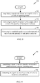
FIG. 4 illustrates the power amplifier module ofFIG. 3 during operation in a high-power mode. -
FIG. 5 illustrates the power amplifier module ofFIG. 3 during operation in a medium-power mode. -
FIG. 6 illustrates the power amplifier module ofFIG. 3 during operation in a low-power mode. -
FIG. 7 is a plot depicting power added efficiency in relation to output power for a conventional amplifier module and the power amplifier module ofFIG. 3 . -
FIG. 8 is a flowchart illustrating a method, according to an exemplary embodiment of the present invention. -
FIG. 9 is a flowchart illustrating another method, according to an exemplary embodiment of the present invention. - The detailed description set forth below in connection with the appended drawings is intended as a description of exemplary embodiments of the present invention and is not intended to represent the only embodiments in which the present invention can be practiced. The term "exemplary" used throughout this description means "serving as an example, instance, or illustration," and should not necessarily be construed as preferred or advantageous over other exemplary embodiments. The detailed description includes specific details for the purpose of providing a thorough understanding of the exemplary embodiments of the invention. It will be apparent to those skilled in the art that the exemplary embodiments of the invention may be practiced without these specific details. In some instances, well-known structures and devices are shown in block diagram form in order to avoid obscuring the novelty of the exemplary embodiments presented herein.
- A multi-mode multi-band power amplifier (PA) module capable of supporting multiple modes and multiple frequency bands is described herein. The PA module may be used for various electronics devices such as wireless communication devices, cellular phones, personal digital assistants (PDAs), handheld devices, wireless modems, laptop computers, cordless phones, Bluetooth devices, consumer electronics devices, etc. For clarity, the use of the PA module in a wireless communication device is described below.
- Exemplary embodiments, as described herein, are directed to an enhanced multi-mode, multi-band power amplifier module. According to one exemplary embodiment, an amplifier module may include a transmit path including a first amplifier and a second amplifier. The amplifier module may also include a transformer coupled between the first amplifier and the second amplifier and switchably configured for coupling the first amplifier in series with the second amplifier in a first mode and coupling the first amplifier to bypass the second amplifier in a second mode.
-
FIG. 1 shows a block diagram of an exemplary design of awireless communication device 50. In this exemplary embodiment,wireless device 50 includes adata processor 52 and atransceiver 56.Transceiver 56 includes atransmitter 58 comprising up-converter circuits 60 and aPA module 62.Transceiver 56 further includes a receiver 64 comprising a front-end module 68 and down-converter circuits 66. In general,wireless device 50 may include any number of transmitters and any number of receivers for any number of communication systems and any number of frequency bands. - In the transmit path,
data processor 52 may process data to be transmitted and provide an output baseband signal totransmitter 58. Withintransmitter 58, up-converter circuits 60 may process (e.g., amplify, filter, and frequency up-convert) the output baseband signal and provide an input RF signal. Up-converter circuits 60 may include amplifiers, filters, mixers, etc.PA module 62 may amplify the input RF signal to obtain the desired output power level and provide an output RF signal, which may be transmitted via anantenna 70.PA module 62 may include driver amplifiers, power amplifiers, switches, etc., as described below. - In the receive path,
antenna 70 may receive RF signals transmitted by base stations and/or other transmitter stations and may provide a received RF signal, which may be routed viaPA module 62 and provided to receiver 64. Within receiver 64, front-end module 68 may process (e.g., amplify and filter) the received RF signal and provide an amplified RF signal. Front-end module 68 may include duplexers, low noise amplifiers (LNA), etc. Down-converter circuits 66 may further process (e.g., frequency down-convert, filter, and amplify) the amplified RF signal and provide an input baseband signal todata processor 52. Down-converter circuits 66 may include mixers, filters, amplifiers, etc.Data processor 52 may further process (e.g., digitize, demodulate, and decode) the input baseband signal to recover transmitted data. - A
control unit 72 may receive control information fromdata processor 52 and may generate controls for the circuits and modules intransmitter 58 and receiver 64.Data processor 52 may also provide controls directly to the circuits and modules intransmitter 58 and receiver 64. In any case, the controls may direct the operation of the circuits and modules to obtain the desired performance. -
FIG. 1 shows an exemplary design oftransmitter 58 and receiver 64. In general, the conditioning of the signals intransmitter 58 and receiver 64 may be performed by one or more stages of amplifiers, filters, mixers, etc. These circuit blocks may be arranged in various configurations. All or a portion oftransmitter 58 and all or a portion of receiver 64 may be implemented on one or more analog integrated circuits (ICs), one or more RF ICs (RFICs), one or more mixed-signal ICs, etc. For example,PA module 62 may be implemented on one RFIC, and up-converter circuits 60 and down-converter circuits 66 may be implemented on another RFIC. -
Data processor 52 may perform various functions forwireless device 50, e.g., processing for data being transmitted or received. Amemory 54 may store program codes and data fordata processor 52.Data processor 52 may be implemented on one or more application specific integrated circuits (ASICs) and/or other ICs. -
Wireless device 50 may support multiple modes and multiple bands.PA module 62 may be designed to support all of the modes and bands supported bywireless device 50. The multiple modes may correspond to different radio technologies such as Code Division Multiple Access (CDMA) IX, Wideband CDMA (WCDMA), Global System for Mobile Communications (GSM), Long Term Evolution (LTE), Wireless Local Area Network (WLAN), etc. Each mode may correspond to a particular radio technology, which may utilize frequency division duplexing (FDD) or time division duplexing (TDD). For FDD, different frequency channels are used for the downlink and uplink, and a duplexer may be used to route an output RF signal from a transmitter to an antenna and to route a received RF signal from the antenna to a receiver. For TDD, the same frequency channel is used for both the downlink and uplink, and a switch may be used to couple the transmitter to the antenna some of the time and to couple the receiver to the antenna some other time. -
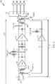
FIG. 2 illustrates apower amplifier module 100.Power amplifier module 100 includes a single-endedinput 102 coupled to a first end of a primary winding TAP of a transformer TA via a capacitor C1. A second end of primary winding TAP of a transformer TA is coupled to a switch S1. A secondary winding TAS of transformer TA is coupled to an input of adriver amplifier 104.Power amplifier module 100 further includes a capacitors C2-C5 and inductors L1-L3. In addition,power amplifier module 100 includes apower amplifier 106 coupled between capacitor C5 and a capacitor C6. Moreover,power amplifier module 100 includes another transformer TB having a primary winding TBP coupled to capacitor C6 and a second winding TBS coupled to each of a switch S2 and a switch S3.Power amplifier module 100 also includes anamplifier 112 coupled between capacitors C7 and C8, and an inductor L4 coupled between an output ofamplifier 112 and a supply voltage VDD_BYP. - Switch S1 of
power amplifier module 100 is configured to couple the second end of primary winding TAP of transformer TA to either a ground voltage GRND or capacitor C7. Further, switch S2 is ofpower amplifier module 100 is configured to couple one end of secondary winding TBS of transformer TB to either ground voltage GRND or capacitor C8. Moreover, switch S3 ofpower amplifier module 100 is configured to couple another end of secondary winding TBS of transformer TB to one of a plurality of ports B1-B4 for selecting a desired frequency band. - During a contemplated operation of power amplifier module 100 (i.e., a high-power mode), switch S1 and switch S2 are coupled to ground voltage GRND, and therefore, a signal received at
input 102 is conveyed throughdriver amplifier 104 andpower amplifier 106 to one of ports B1-B4, depending on a selected frequency band. A high-power path is depicted byarrow 108. During another contemplated operation of power amplifier module 100 (i.e., either a medium-power mode or a low-power mode), switch S1 is coupled to capacitor C7 and switch S2 is coupled to capacitor C8 and, therefore, a signal received atinput 102 bypassesdriver amplifier 104 andpower amplifier 106, and is conveyed throughamplifier 112 to one of ports B1-B4, depending on a selected frequency band. Medium and low-power paths are depicted byarrow 110. - As will be appreciated by a person having ordinary skill in the art, conventional power amplifier architectures may suffer from lower performance as the number of required frequency bands increases. Further, conventional power amplifier architectures may include a first path for high-power operation and a second path, which is used for both medium and low-power modes. However, because the second path supports both medium and low-power modes, neither low-power nor medium-power modes may be optimized. Stated another way, in order to support both medium and low-power modes, the second path includes a trade-off between low-power mode PAE and the output power of the medium-power mode. In addition, multi-port switches of conventional power amplifier architectures (e.g., switch S3 of power amplifier module 100) may have a higher insertion loss as the number of required frequency bands increases.
-
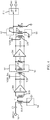
FIG. 3 illustratespower amplifier module 200, according to an exemplary embodiment of the present invention.Power amplifier module 200 includes aninput 202 coupled to a first end of primary winding TIP of a transformer T1 via capacitor C1. A second end of primary winding TIP of a transformer T1 is coupled to a switch S4. Further a secondary winding T1S of transformer T1 is coupled to adriver amplifier 204. It is noted that primary winding TIP of a transformer T1 is configured to receive a single-ended signal frominput 102 and secondary winding T1S of transformer T1 is configured to convey a double-ended signal todriver amplifier 204.Power amplifier module 200 further includes capacitor C2 coupled in parallel with each of an output ofdriver amplifier 204 and a primary winding T2P of a transformer T2. In addition, a center tap of primary winding T2P of transformer T2 is coupled to a supply voltage VDD_DA. -
Power amplifier module 200 also includes capacitors C5 and C6, apower amplifier 206, a transformer T3, and switches S5-S8. As illustrated, a first end of secondary winding T2S of transformer T2 is switchably coupled to either an input of apower amplifier 206 via switch S5 or a secondary winding T3S transformer T3 via switch S5 and switch S7. Further, a second end of secondary winding T2S of transformer T2 is switchably coupled to either an input of apower amplifier 206 via switch S6 or a secondary winding T3S transformer T3 via switch S6 and switch S8. It is noted that switch S5 may couple secondary winding T2S of transformer T2 to eitherpower amplifier 206, switch S7, or ground voltage GRND. Further, switch S6 may couple secondary winding T2S of transformer T2 to eitherpower amplifier 206, switch S8, or ground voltage GRND. Additionally, an output ofpower amplifier 206 is coupled in parallel with capacitor C6 and a primary winding T3P of transformer T3. Furthermore, a center tap of primary winding T3P of transformer T3 is coupled to a supply voltage VDD_PA. -
Power amplifier module 200 further includes capacitors C7-C9,amplifier 212, inductor L4, and switches S9-S11. As an example,amplifier 212 may comprise a low-power amplifier. As depicted, switch S4 is configured to couple the second end of primary winding TIP of transformer T1 to either a ground voltage or capacitor C7, which is coupled to an input ofamplifier 212. Moreover, an output ofamplifier 212 is coupled to capacitor C8, which is further coupled to a supply voltage VDD_BYP via inductor L4. Switch S9 is configured to couple an output ofamplifier 112 to switch S11 and switch S10 is configured to couple the output ofamplifier 112 to switch S12.Power amplifier module 200 further includes a switch S13 for coupling areceiver port 220 to either band port B1 or band port B2, and a switch S14 for coupling areceiver port 222 to either band port B3 or band port B4. - According to various exemplary embodiments of the present invention,
power amplifier module 200 may be configured to operate in one a plurality of modes and in one of a plurality of bands. As described more fully with respect toFIGS. 4-6 , during a high-power mode,power amplifier module 200 may be configured to convey a signal received viainput 102 to one of a plurality of band ports (i.e., one of frequency band ports B1-B4) viadriver amplifier 204 and power amplifier 203. Moreover, during a medium-power mode,power amplifier module 200 may be configured to convey a signal received viainput 102 to one of a plurality of band ports (i.e., one of frequency band ports B1-B4) viadriver amplifier 204. Further, during a low-power mode,power amplifier module 200 may be configured to convey a signal received viainput 102 to one of a plurality of band ports (i.e., one of frequency band ports B1-B4) viaamplifier 212. -
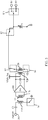
FIG. 4 illustratespower amplifier module 200 configured for operation in a high-power mode. It is noted that in the high-power mode configuration illustrated inFIG. 4 , switch S4 couples one end of primary winding TIP of transformer T1 to ground voltage GRND, switches S5 and S6 couple secondary winding T2S of transformer T2 topower amplifier 206, switch S8 couples one end of secondary winding T3S of transformer T3 to ground voltage GRND, and switch S7 couples another end of secondary winding T3S of transformer T3 to switch S11, which is configured for selecting either a first band port B1 or a second band port B2. - A contemplated operation of
power amplifier module 200 in a high-power mode will now be described. Upon receipt of a signal atinput 202,power amplifier module 200 may convey a single-ended signal to primary winding TIP of transformer T1. Via inductive coupling, as will be appreciated by a person having ordinary skill in the art, a voltage may be induced in secondary winding T1S of transformer T1 and a double-ended signal may be conveyed todriver amplifier 104. After being amplified bydriver amplifier 204, the double-ended signal may be conveyed to transformer T2, which may convey the signal topower amplifier 206. It is noted that transformer T2, which is switchably configured to coupleddriver amplifier 204 topower amplifier 206, may provide impedance matching forpower amplifier 206. Furthermore, capacitor C5 may be tunable as an interstage matching component, and capacitor C9 may be tunable as an output matching component for band tuning. Accordingly, exemplary embodiments of the present invention include transformer-based impedance matching.Power amplifier 206 may amplify the signal and convey a double-ended output that is received by primary winding T3P of transformer T3. Moreover, secondary winding T3S of transformer T3 may convey a single-ended signal to switch S11, which, as noted above, may be configured to select either first band port B1 or second band port B2. - Although
power amplifier module 200 is illustrated inFIG. 4 as being configured for operation in either a first frequency band (i.e., via band port B1) or a second frequency band (i.e., via band port B2), the invention is not so limited. Rather,power amplifier module 200 may be configured for operation in one of any number of bands. For example, with reference toFIG. 3 , in a different configuration, which may enablepower amplifier module 200 to operate in a high-power mode and in either a third band (i.e., via third band port B3) or a fourth band (i.e., via fourth band port B4), switch S4 couples one end of primary winding of primary winding TIP of transformer T1 to ground voltage GRND, switches S5 and S6 couple secondary winding T2S of transformer T2 topower amplifier 206, switch S7 couples one end of secondary winding T3S of transformer T3 to ground voltage GRND, and switch S8 couples another end of secondary winding T3S of transformer T3 to switch S12, which is configured for selecting either third band port B3 or fourth band port B4. -
FIG. 5 illustratespower amplifier module 200 configured for operation in a medium-power mode. It is noted in the medium-power mode configuration illustrated inFIG. 5 , switch S4 couples one end of primary winding of primary winding TIP of transformer T1 to ground voltage GRND, switch S6 couples one end of secondary winding T2S of transformer T2 to ground voltage GRND, and switches S5 and S7 couple another end of secondary winding T2S of transformer T2 to switch S11, which is configured for selecting either a first band port B1 or a second band port B2. - A contemplated operation of
power amplifier module 200 in a medium-power mode will now be described. Upon receipt of a signal atinput 202,power amplifier module 200 may convey a single-ended signal to primary winding TIP of transformer T1. Via inductive coupling, as will be appreciated by a person having ordinary skill in the art, a voltage may be induced in secondary winding T1S of transformer T1 and a double-ended signal may be conveyed todriver amplifier 204. After being amplified bydriver amplifier 204, the double-ended signal may be conveyed to transformer T2, which may convey a single-ended signal to switch S11, which, as noted above, may be configured to select either first band port B1 or second band port B2. With reference toFIGS. 3 and4 , it is noted that, in medium-power mode, transformer T2 is switchably configured to bypasspower amplifier 206. - Although
power amplifier module 200 is illustrated inFIG. 5 as being configured for operation in either a first band (i.e., via band port B1) or a second band (i.e., via band port B2), the invention is not so limited. Rather,power amplifier module 200 may be configured for operation in one of any number of bands. For example, with reference toFIG. 3 , in a different configuration, which may enablepower amplifier module 200 to operate in a medium-power mode and in either a third band (i.e., third band port B3) or a fourth band (i.e., via fourth band port B4), switch S4 couples one end of primary winding of primary winding TIP of transformer T1 to ground voltage GRND, switch S5 couples one end of secondary winding T2S of transformer T2 to ground voltage GRND, and switches S6 and S8 couple another end of secondary winding T2S of transformer T2 to switch S12, which is configured for selecting either third band port B3 or fourth band port B4. -
FIG. 6 illustratespower amplifier module 200 configured for operation in a low-power mode. It is noted that in the low-power mode configuration illustrated inFIG. 5 , switch S4 couples one end of primary winding of primary winding TIP of transformer T1 to amplifier 212 (i.e., via capacitor C7). Further, switches S9-S12 may be configured for coupling an output ofamplifier 212 to one of a plurality of band ports B1-B4. - A contemplated operation of
power amplifier module 200 in a low-power mode will now be described. Upon receipt of a signal atinput 202,power amplifier module 200 may convey a single-ended signal toamplifier 212 via primary winding TIP of transformer T1 and capacitor C7. After being amplified byamplifier 212, the signal may be conveyed to switches S10 and S9. In one configuration (i.e., if either a first band port B1 or a second band port B2 is selected), switch S10 may be coupled to ground voltage GRND and switch S9 may couple the output ofamplifier 212 to switch S11, which, may be configured to select either first band port B1 or second band port B2. In another configuration (i.e., if either a third band port B3 or a fourth band port B4 is selected), switch S9 may be coupled to ground voltage GRND and switch S10 may couple the output ofamplifier 212 to switch S12, which may be configured to select either third band port B3 or fourth band port B4. - The exemplary embodiments of the present invention provide for dedicated transmit paths for each of high, medium, and low-power modes. Accordingly, each path may be optimized accordingly. Further, exemplary embodiments provide for inter-stage impedance matching based on a switchable transformer, which may result in wider bandwidth without adding any devices. Therefore, the output power can be easily tuned to meet long term evolution (LTE) requirements without hurting low-power mode performance. Additionally, exemplary embodiments include multi-port transmitter switch devices (i.e., switches S11 and S12), which can be split into two output ports of a transformer (i.e., transformer T2 or T3), thus resulting in the substantial reduction of insertion loss compared to conventional amplifier switches. It is noted that
receiver switch ports - Each of the high, medium, and low-power modes are implemented in a compact form factor, and, due to the balanced structure, medium and high-power modes mode may be immune to parasitic ground inductance. Additionally, the low-power mode may be optimized for a low quiescent current requirement and medium-power mode may be optimized based on an output power capability of
driver amplifier 204. Further, transmit band ports are split into two branches of an output transformer (i.e., transformer T2 in medium-power mode and transformer T3 in high-power mode). Therefore, insertion loss may be reduced compared to conventional structures and, thus, PAE at high power improves substantially. - With specific reference to
FIG. 3 , the differential design ofpower amplifier 206 may reduce ground inductance and output matching network (OMN) loss due to a higher load line. Further, transformer T3 may provide output matching for multi-band support and may stabilize power combining with smaller devices. In addition, higher load line & smaller transformation ratio may minimize OMN loss. Moreover, transformer T3 may be implemented with a high Q substrate layer. Furthermore, a switchable transformer based antenna switch module (ASM) (i.e., switches S11 and S12 and either transformer T2 or transformer T3) may minimize loss. Moreover,amplifier 212, which is configured for single-ended operation, may minimize quiescent current and may only require a relatively small area. -
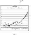
FIG. 7 is a plot 400 depicting power added efficiency (PAE) relative to output power (Pout) for a conventional amplifier module and an amplifier module in accordance with an exemplary embodiment of the present invention. More specifically, waveform 402 depicts PAE versus Pout for a conventional amplifier module and waveform 404 depicts PAE versus Pout for an amplifier module in accordance with an exemplary embodiment of the present invention (e.g., amplifier module 200). As shown in plot 400, PAE in low-power mode (i.e., from 0 dBm to approximately 7 dBm) is higher for waveform 404 due to the optimized device size in a separate path (i.e., the low-power mode transmit path). Further, Pout is higher for waveform 404 in medium-power mode (i.e., from approximately 7 dBm to 17 dBm) due to the optimized device size of a driver amplifier (e.g., driver amplifier 204). In addition, in high-power mode (i.e., from approximately 17 dBm to 29 dBm), waveform 404 has a larger PAE due to less insertion loss from a split switch configuration (i.e., switches S11 and S12 ofmodule 200 ofFIG. 3 compared to switch S3 ofmodule 100 ofFIG. 2 ). -
FIG. 8 is a flowchart illustrating amethod 700, in accordance with one or more exemplary embodiments.Method 700 may include amplifying a signal with at least one amplifier in of a plurality of operating modes (depicted by numeral 702).Method 700 may also include conveying the amplified signal to a first output path if one of a first plurality of band ports is selected (depicted by numeral 704). In addition,method 700 may include conveying the amplified signal to a second output path if one of a second plurality of band ports is selected (depicted by numeral 706). -
FIG. 9 is a flowchart illustrating anothermethod 750, in accordance with one or more exemplary embodiments.Method 750 may include amplifying a signal in one of a plurality of selectable paths based on a selected operating mode (depicted by numeral 752).Method 750 may also include outputting the signal via one of a plurality of switches based on a selected band (depicted by numeral 754). - Those of skill in the art would understand that information and signals may be represented using any of a variety of different technologies and techniques. For example, data, instructions, commands, information, signals, bits, symbols, and chips that may be referenced throughout the above description may be represented by voltages, currents, electromagnetic waves, magnetic fields or particles, optical fields or particles, or any combination thereof.
- Those of skill would further appreciate that the various illustrative logical blocks, modules, circuits, and algorithm steps described in connection with the exemplary embodiments disclosed herein may be implemented as electronic hardware, computer software, or combinations of both. To clearly illustrate this interchangeability of hardware and software, various illustrative components, blocks, modules, circuits, and steps have been described above generally in terms of their functionality. Whether such functionality is implemented as hardware or software depends upon the particular application and design constraints imposed on the overall system. Skilled artisans may implement the described functionality in varying ways for each particular application, but such implementation decisions should not be interpreted as causing a departure from the scope of the exemplary embodiments of the invention.
- The various illustrative logical blocks, modules, and circuits described in connection with the exemplary embodiments disclosed herein may be implemented or performed with a general purpose processor, a Digital Signal Processor (DSP), an Application Specific Integrated Circuit (ASIC), a Field Programmable Gate Array (FPGA) or other programmable logic device, discrete gate or transistor logic, discrete hardware components, or any combination thereof designed to perform the functions described herein. A general purpose processor may be a microprocessor, but in the alternative, the processor may be any conventional processor, controller, microcontroller, or state machine. A processor may also be implemented as a combination of computing devices, e.g., a combination of a DSP and a microprocessor, a plurality of microprocessors, one or more microprocessors in conjunction with a DSP core, or any other such configuration.
- In one or more exemplary embodiments, the functions described may be implemented in hardware, software, firmware, or any combination thereof. If implemented in software, the functions may be stored on or transmitted over as one or more instructions or code on a computer readable medium. Computer readable media includes both computer storage media and communication media including any medium that facilitates transfer of a computer program from one place to another. A storage media may be any available media that can be accessed by a computer. By way of example, and not limitation, such computer readable media can comprise RAM, ROM, EEPROM, CD ROM or other optical disk storage, magnetic disk storage or other magnetic storage devices, or any other medium that can be used to carry or store desired program code in the form of instructions or data structures and that can be accessed by a computer. Also, any connection is properly termed a computer readable medium. For example, if the software is transmitted from a website, server, or other remote source using a coaxial cable, fiber optic cable, twisted pair, digital subscriber line (DSL), or wireless technologies such as infrared, radio, and microwave, then the coaxial cable, fiber optic cable, twisted pair, DSL, or wireless technologies such as infrared, radio, and microwave are included in the definition of medium. Disk and disc, as used herein, includes compact disc (CD), laser disc, optical disc, digital versatile disc (DVD), floppy disk and blu ray disc where disks usually reproduce data magnetically, while discs reproduce data optically with lasers. Combinations of the above should also be included within the scope of computer readable media.
- The previous description of the disclosed exemplary embodiments is provided to enable any person skilled in the art to make or use the present invention. Various modifications to these exemplary embodiments will be readily apparent to those skilled in the art, and the generic principles defined herein may be applied to other embodiments without departing from the scope of the invention. Thus, the present invention is not intended to be limited to the exemplary embodiments shown herein but is to be accorded the widest scope consistent with the principles and novel features disclosed in the appended claims herein.
Claims (15)
- An apparatus (200), comprising:a transmit path including a first amplifier (204) and a second amplifier (206); anda transformer (T2) comprising a primary winding (T2P) and a secondary winding (T2S) and coupled between the output of the first amplifier (204) and the input of the second amplifier (206) and switchably configured to double-endedly couple the first amplifier (204) in series with the second amplifier (206) in a first mode and to single-endedly couple the first amplifier (204) to bypass the second amplifier (206) through one end of the secondary winding (T2S) of the transformer (T2) and to couple another end of the secondary winding (T2S) to ground in a second mode.
- The apparatus (200) of claim 1, further comprising another transmit path including a third amplifier (212) for operating in a third mode.
- The apparatus (200) claim 2, further comprising:a first switch (S9) for coupling either the transmit path or the another transmit path to one of a first band port and a second band port; anda second switch (S10) for coupling either the transmit path or the another transmit path to one of a third band port and a fourth band port.
- The apparatus (200) of claim 2, the first mode comprising a high-power mode, the second mode comprising a medium-power mode, and the third mode comprising a low-power mode.
- The apparatus (200) of claim 1, the transmit path including:
a second transformer (T1) for receiving a single-ended input signal and conveying a double-ended output signal to the first amplifier (204), further including a third transformer (T3) for receiving a double-ended input signal conveyed from the second amplifier (206) and conveying a single-ended signal to an output. - The apparatus (200) of claim 1, the transformer (T2) for receiving the output signal and switchably configured for either conveying a double-ended signal to the second amplifier in the first mode or conveying a single-ended signal to bypass the second amplifier (206) in the second mode.
- The apparatus (200) of claim 1, further comprising a first switch for coupling to an output of either the first amplifier or the second amplifier and for selecting either a first band or a second band and a second, different switch for coupling to an output of either the first amplifier of the second amplifier and for selecting either a third band or a fourth band.
- A method (700), comprising:amplifying (702) a signal with at least a first amplifier and a second amplifier and a transformer (T2) coupled between the output of the first amplifier and the input of the second amplifier in each one of a plurality of operating modes, the transformer (T2) double-endedly coupling a first amplifier (204) in series with a second amplifier (206) in a first operating mode and the transformer (T2) single-endedly coupling the first amplifier (204) to bypass the second amplifier (206) through one end of the secondary winding (T2S) of the transformer (T2) and coupling another end of the secondary winding (T2S) to ground in a second operating mode; andconveying (704) the amplified signal to a first output path if one of a first plurality of band ports is selected; andconveying (706) the amplified signal to a second output path if one of a second plurality of band ports is selected.
- The method (700) of claim 8, the amplifying comprising:
amplifying the signal with the first amplifier (204) and the second amplifier (206) in a first operating mode;amplifying the signal with the first amplifier in the second operating mode; andamplifying the signal with a third amplifier (212) in a third operating mode. - The method (700) of claim 9, further comprising switchably configuring the transformer (T2) to convey a signal output from the first amplifier (204) to the second amplifier (206) in the first operating mode.
- The method (700) of claim 9, further comprising switchably configuring the transformer (T2) to convey a signal output from the first amplifier (204) to one of the first output path and the second output path in the second operating mode.
- The method (700) of claim 8, the amplifying comprising:
converting a single-ended signal to a double-ended signal at a second transformer (T1); and
converting an amplified double-ended signal to a single-ended signal at the transformer (T2). - The method (700) of claim 8, further comprising outputting the signal via one of a plurality of switches based on a selected band, the outputting comprising one of outputting the signal via a first switch if one of a first band and a second band is selected and outputting the signal via a second switch if one of a third band and a fourth band is selected.
- The method (700) of claim 8, further comprising providing impedance matching from an output of the first amplifier to an input of the second amplifier in a high-power mode, wherein the first amplifier is a driver amplifier and the second amplifier is a power amplifier.
- The method (700) of claim 8, tuning a capacitor to provide at least one of interstage matching and output matching for the at least one amplifier.
Applications Claiming Priority (2)
| Application Number | Priority Date | Filing Date | Title |
|---|---|---|---|
| US13/720,851 US9160377B2 (en) | 2012-12-19 | 2012-12-19 | Multi-mode multi-band power amplifiers |
| PCT/US2013/076749 WO2014100513A1 (en) | 2012-12-19 | 2013-12-19 | Multi-mode multi-band power amplifiers |
Publications (2)
| Publication Number | Publication Date |
|---|---|
| EP2936679A1 EP2936679A1 (en) | 2015-10-28 |
| EP2936679B1 true EP2936679B1 (en) | 2018-10-17 |
Family
ID=49956436
Family Applications (1)
| Application Number | Title | Priority Date | Filing Date |
|---|---|---|---|
| EP13821320.2A Active EP2936679B1 (en) | 2012-12-19 | 2013-12-19 | Multi-mode multi-band power amplifiers |
Country Status (5)
| Country | Link |
|---|---|
| US (1) | US9160377B2 (en) |
| EP (1) | EP2936679B1 (en) |
| JP (1) | JP6017704B2 (en) |
| CN (1) | CN104854790B (en) |
| WO (1) | WO2014100513A1 (en) |
Families Citing this family (34)
| Publication number | Priority date | Publication date | Assignee | Title |
|---|---|---|---|---|
| US9444498B2 (en) * | 2012-12-03 | 2016-09-13 | Broadcom Corporation | Repartitioned transceiver using silicon-on-insulator |
| US9178555B2 (en) * | 2013-02-20 | 2015-11-03 | Micro Mobio Corporation | World band radio frequency front end module, system and method thereof |
| US9515615B2 (en) | 2013-02-20 | 2016-12-06 | Micro Mobio Corporation | World band radio frequency front end module, system and method thereof |
| US10643962B1 (en) | 2013-02-20 | 2020-05-05 | Micro Mobio Corporation | World band radio frequency front end module, system and method of power sensing thereof |
| US10027287B1 (en) | 2013-02-20 | 2018-07-17 | Micro Mobio Corporation | World band frequency front end module, system and method thereof |
| US9425835B2 (en) * | 2013-08-09 | 2016-08-23 | Broadcom Corporation | Transmitter with reduced counter-intermodulation |
| JP6291796B2 (en) * | 2013-11-08 | 2018-03-14 | 株式会社ソシオネクスト | amplifier |
| US9595933B2 (en) * | 2013-12-30 | 2017-03-14 | Lansus Technologies Inc. | Power amplifier device and circuits |
| US9590569B2 (en) * | 2014-05-06 | 2017-03-07 | Skyworks Solutions, Inc. | Systems, circuits and methods related to low power efficiency improvement in multi-mode multi-band power amplifiers |
| US9356560B2 (en) * | 2014-08-01 | 2016-05-31 | Qualcomm Incorporated | Multi-mode integrated power amplifier |
| US9548767B2 (en) | 2014-11-04 | 2017-01-17 | Qualcomm Incorporated | Multi-band amplifier |
| KR102123600B1 (en) * | 2015-05-29 | 2020-06-15 | 삼성전기주식회사 | Front end circuit |
| US9543900B1 (en) | 2015-06-19 | 2017-01-10 | Qualcomm Incorporated | Switchable supply and tunable load impedance power amplifier |
| US10103754B2 (en) * | 2016-07-17 | 2018-10-16 | Skyworks Solutions, Inc. | Architectures and methods related to transmit signal routing with re-use of filters |
| US10177723B2 (en) | 2016-08-30 | 2019-01-08 | Qualcomm Incorporated | Reconfigurable power amplifier |
| US10256783B2 (en) * | 2016-11-29 | 2019-04-09 | Taiwan Semiconductor Manufacturing Co., Ltd. | Dual-mode RF transmission frontend |
| JP2018137566A (en) * | 2017-02-21 | 2018-08-30 | 株式会社村田製作所 | Power amplifier circuit |
| US10230300B2 (en) * | 2017-04-25 | 2019-03-12 | Cirrus Logic, Inc. | Power converter predriver system with multiple power modes |
| US10110177B1 (en) * | 2017-07-28 | 2018-10-23 | Silicon Laboratories Inc. | Programmable impedance control for a transformer |
| US11476814B2 (en) * | 2018-01-23 | 2022-10-18 | Teknologian tukimuskeskus VTT Oy | Transformer based switches and systems for PALNA transceivers |
| CN109196783B (en) * | 2018-04-12 | 2020-04-24 | 深圳市汇顶科技股份有限公司 | Multi-mode configurable transceiver with low voltage switch and method of configuring the same |
| US10333579B1 (en) * | 2018-04-12 | 2019-06-25 | Shenzhen GOODIX Technology Co., Ltd. | Multi-mode configurable transceiver with low voltage switches |
| TWI820181B (en) * | 2018-08-13 | 2023-11-01 | 美商天工方案公司 | Loadline switchable push/pull power amplifier |
| US11671061B2 (en) * | 2018-09-26 | 2023-06-06 | Skyworks Solutions, Inc. | Load-line switching for push-pull power amplifiers |
| JP7275624B2 (en) * | 2019-02-13 | 2023-05-18 | 株式会社デンソー | Frequency band variable high frequency amplifier |
| RU2710292C1 (en) * | 2019-05-22 | 2019-12-25 | федеральное государственное бюджетное образовательное учреждение высшего образования "Донской государственный технический университет" (ДГТУ | Low-sensitivity active rc-filter of second order based on two multi-differential operational amplifiers |
| RU2710852C1 (en) * | 2019-05-23 | 2020-01-14 | федеральное государственное бюджетное образовательное учреждение высшего образования "Донской государственный технический университет" (ДГТУ) | Low-sensitivity second-order arc filter based on two multi-differential operational amplifiers |
| US11050387B2 (en) * | 2019-09-09 | 2021-06-29 | Texas Instruments Incorporated | Integrated circuit devices with parallel power amplifier output paths |
| RU2720559C1 (en) * | 2019-11-22 | 2020-05-12 | федеральное государственное бюджетное образовательное учреждение высшего образования "Донской государственный технический университет" (ДГТУ) | Active rc-low-pass filter with single-element frequency tuning of the pole on the differential and two multi-differential operational amplifiers |
| CN112398777B (en) * | 2020-10-21 | 2023-02-03 | 中交航信(上海)科技有限公司 | Very high frequency data exchange system |
| US11606109B2 (en) * | 2021-04-22 | 2023-03-14 | Texas Instruments Incorporated | Dynamically configurable transmitter power levels |
| US20230049925A1 (en) * | 2021-08-16 | 2023-02-16 | Qualcomm Incorporated | Multi-mode multi-port driver for transceiver interface |
| WO2023068079A1 (en) * | 2021-10-22 | 2023-04-27 | 株式会社村田製作所 | High frequency circuit, and communication device |
| US20230170926A1 (en) * | 2021-11-30 | 2023-06-01 | Raytheon Company | Differential probe with single transceiver antenna |
Family Cites Families (15)
| Publication number | Priority date | Publication date | Assignee | Title |
|---|---|---|---|---|
| JPH07115331A (en) * | 1993-10-19 | 1995-05-02 | Mitsubishi Electric Corp | Amplifying device |
| DE69630512T2 (en) * | 1995-09-29 | 2004-05-06 | Matsushita Electric Industrial Co., Ltd., Kadoma | POWER AMPLIFIER AND COMMUNICATION DEVICE |
| JPH09148852A (en) * | 1995-11-24 | 1997-06-06 | Matsushita Electric Ind Co Ltd | Transmission output variable device |
| JP3587346B2 (en) * | 1998-08-07 | 2004-11-10 | 松下電器産業株式会社 | Wireless communication device and transmission power control method in wireless communication device |
| US6625430B2 (en) * | 1998-12-15 | 2003-09-23 | Ericsson Inc. | Method and apparatus for attaining higher amplifier efficiencies at lower power levels |
| US8130043B2 (en) | 2003-09-25 | 2012-03-06 | Anadigics, Inc. | Multi-stage power amplifier with enhanced efficiency |
| DE10361660A1 (en) | 2003-12-30 | 2005-02-03 | Infineon Technologies Ag | Power signal amplifier for use in mobile radio frequency equipment is based on multiple amplifier stages in parallel |
| US8280325B2 (en) | 2006-06-23 | 2012-10-02 | Broadcom Corporation | Configurable transmitter |
| US7630693B2 (en) * | 2006-11-16 | 2009-12-08 | Freescale Semiconductor, Inc. | Transmitter with improved power efficiency |
| US7952433B2 (en) | 2008-11-25 | 2011-05-31 | Samsung Electro-Mechanics Company | Power amplifiers with discrete power control |
| US8068795B2 (en) * | 2009-03-24 | 2011-11-29 | Freescale Semiconductor, Inc. | RF multiband transmitter with balun |
| US8536950B2 (en) | 2009-08-03 | 2013-09-17 | Qualcomm Incorporated | Multi-stage impedance matching |
| US8149050B2 (en) | 2009-11-13 | 2012-04-03 | Qualcomm, Incorporated | Cascaded amplifiers with transformer-based bypass mode |
| US7944296B1 (en) | 2010-03-12 | 2011-05-17 | Samsung Electro-Mechanics Company | Low power mode amplification with a transformer output matching and a virtual ground |
| JPWO2012098863A1 (en) * | 2011-01-20 | 2014-06-09 | パナソニック株式会社 | High frequency power amplifier |
-
2012
- 2012-12-19 US US13/720,851 patent/US9160377B2/en active Active
-
2013
- 2013-12-19 WO PCT/US2013/076749 patent/WO2014100513A1/en active Application Filing
- 2013-12-19 EP EP13821320.2A patent/EP2936679B1/en active Active
- 2013-12-19 CN CN201380065958.2A patent/CN104854790B/en active Active
- 2013-12-19 JP JP2015549748A patent/JP6017704B2/en active Active
Non-Patent Citations (1)
| Title |
|---|
| None * |
Also Published As
| Publication number | Publication date |
|---|---|
| CN104854790A (en) | 2015-08-19 |
| US9160377B2 (en) | 2015-10-13 |
| CN104854790B (en) | 2017-06-30 |
| US20150050901A1 (en) | 2015-02-19 |
| JP2016501503A (en) | 2016-01-18 |
| JP6017704B2 (en) | 2016-11-02 |
| EP2936679A1 (en) | 2015-10-28 |
| WO2014100513A1 (en) | 2014-06-26 |
Similar Documents
| Publication | Publication Date | Title |
|---|---|---|
| EP2936679B1 (en) | Multi-mode multi-band power amplifiers | |
| EP2959578B1 (en) | Amplifiers with multiple outputs and configurable degeneration inductor | |
| EP3227999B1 (en) | Amplifier with triple-coupled inductors | |
| US9166852B2 (en) | Low noise amplifiers with transformer-based signal splitting for carrier aggregation | |
| EP2949042B1 (en) | Amplifiers with improved isolation | |
| CN102428648B (en) | Output circuit with integrated impedance matching, power combining and filtering for power amplifiers and other circuits | |
| US10177722B2 (en) | Carrier aggregation low-noise amplifier with tunable integrated power splitter | |
| US20150194944A1 (en) | Wideband matching network | |
| CN104067513A (en) | Multi-mode bypass driver amplifier with tunable load matching | |
| CN105409116A (en) | Amplifiers with configurable mutually-coupled source degeneration inductors | |
| US20180048293A1 (en) | Reconfigurable radio frequency (rf) bandstop / intermediate frequency (if) bandpass filter | |
| WO2018031198A1 (en) | Multi-stage bandpass low-noise amplifier | |
| US20210099140A1 (en) | Wide bandwidth radio frequency (rf) amplifier | |
| US20180175798A1 (en) | Area efficient architecture to combine outputs of parallel transmit signal paths | |
| US10122332B2 (en) | Low-noise amplifier with integrated wideband transformer-based power splitter | |
| US20170201408A1 (en) | Wireless receiver for carrier aggregation | |
| US20220302883A1 (en) | Wideband amplifier |
Legal Events
| Date | Code | Title | Description |
|---|---|---|---|
| PUAI | Public reference made under article 153(3) epc to a published international application that has entered the european phase |
Free format text: ORIGINAL CODE: 0009012 |
|
| 17P | Request for examination filed |
Effective date: 20150714 |
|
| AK | Designated contracting states |
Kind code of ref document: A1 Designated state(s): AL AT BE BG CH CY CZ DE DK EE ES FI FR GB GR HR HU IE IS IT LI LT LU LV MC MK MT NL NO PL PT RO RS SE SI SK SM TR |
|
| AX | Request for extension of the european patent |
Extension state: BA ME |
|
| DAX | Request for extension of the european patent (deleted) | ||
| REG | Reference to a national code |
Ref country code: DE Ref legal event code: R079 Ref document number: 602013045333 Country of ref document: DE Free format text: PREVIOUS MAIN CLASS: H03F0003720000 Ipc: H04B0001040000 |
|
| GRAP | Despatch of communication of intention to grant a patent |
Free format text: ORIGINAL CODE: EPIDOSNIGR1 |
|
| RIC1 | Information provided on ipc code assigned before grant |
Ipc: H03F 3/72 20060101ALI20180419BHEP Ipc: H04B 1/04 20060101AFI20180419BHEP Ipc: H03F 1/02 20060101ALI20180419BHEP Ipc: H03H 7/38 20060101ALI20180419BHEP |
|
| INTG | Intention to grant announced |
Effective date: 20180511 |
|
| GRAS | Grant fee paid |
Free format text: ORIGINAL CODE: EPIDOSNIGR3 |
|
| GRAA | (expected) grant |
Free format text: ORIGINAL CODE: 0009210 |
|
| AK | Designated contracting states |
Kind code of ref document: B1 Designated state(s): AL AT BE BG CH CY CZ DE DK EE ES FI FR GB GR HR HU IE IS IT LI LT LU LV MC MK MT NL NO PL PT RO RS SE SI SK SM TR |
|
| REG | Reference to a national code |
Ref country code: GB Ref legal event code: FG4D Ref country code: FR Ref legal event code: PLFP Year of fee payment: 6 |
|
| REG | Reference to a national code |
Ref country code: CH Ref legal event code: EP |
|
| REG | Reference to a national code |
Ref country code: IE Ref legal event code: FG4D |
|
| REG | Reference to a national code |
Ref country code: DE Ref legal event code: R096 Ref document number: 602013045333 Country of ref document: DE Ref country code: AT Ref legal event code: REF Ref document number: 1055192 Country of ref document: AT Kind code of ref document: T Effective date: 20181115 |
|
| REG | Reference to a national code |
Ref country code: NL Ref legal event code: MP Effective date: 20181017 |
|
| REG | Reference to a national code |
Ref country code: LT Ref legal event code: MG4D |
|
| REG | Reference to a national code |
Ref country code: AT Ref legal event code: MK05 Ref document number: 1055192 Country of ref document: AT Kind code of ref document: T Effective date: 20181017 |
|
| PG25 | Lapsed in a contracting state [announced via postgrant information from national office to epo] |
Ref country code: NL Free format text: LAPSE BECAUSE OF FAILURE TO SUBMIT A TRANSLATION OF THE DESCRIPTION OR TO PAY THE FEE WITHIN THE PRESCRIBED TIME-LIMIT Effective date: 20181017 |
|
| PG25 | Lapsed in a contracting state [announced via postgrant information from national office to epo] |
Ref country code: ES Free format text: LAPSE BECAUSE OF FAILURE TO SUBMIT A TRANSLATION OF THE DESCRIPTION OR TO PAY THE FEE WITHIN THE PRESCRIBED TIME-LIMIT Effective date: 20181017 Ref country code: AT Free format text: LAPSE BECAUSE OF FAILURE TO SUBMIT A TRANSLATION OF THE DESCRIPTION OR TO PAY THE FEE WITHIN THE PRESCRIBED TIME-LIMIT Effective date: 20181017 Ref country code: NO Free format text: LAPSE BECAUSE OF FAILURE TO SUBMIT A TRANSLATION OF THE DESCRIPTION OR TO PAY THE FEE WITHIN THE PRESCRIBED TIME-LIMIT Effective date: 20190117 Ref country code: IS Free format text: LAPSE BECAUSE OF FAILURE TO SUBMIT A TRANSLATION OF THE DESCRIPTION OR TO PAY THE FEE WITHIN THE PRESCRIBED TIME-LIMIT Effective date: 20190217 Ref country code: FI Free format text: LAPSE BECAUSE OF FAILURE TO SUBMIT A TRANSLATION OF THE DESCRIPTION OR TO PAY THE FEE WITHIN THE PRESCRIBED TIME-LIMIT Effective date: 20181017 Ref country code: PL Free format text: LAPSE BECAUSE OF FAILURE TO SUBMIT A TRANSLATION OF THE DESCRIPTION OR TO PAY THE FEE WITHIN THE PRESCRIBED TIME-LIMIT Effective date: 20181017 Ref country code: LT Free format text: LAPSE BECAUSE OF FAILURE TO SUBMIT A TRANSLATION OF THE DESCRIPTION OR TO PAY THE FEE WITHIN THE PRESCRIBED TIME-LIMIT Effective date: 20181017 Ref country code: BG Free format text: LAPSE BECAUSE OF FAILURE TO SUBMIT A TRANSLATION OF THE DESCRIPTION OR TO PAY THE FEE WITHIN THE PRESCRIBED TIME-LIMIT Effective date: 20190117 Ref country code: HR Free format text: LAPSE BECAUSE OF FAILURE TO SUBMIT A TRANSLATION OF THE DESCRIPTION OR TO PAY THE FEE WITHIN THE PRESCRIBED TIME-LIMIT Effective date: 20181017 Ref country code: LV Free format text: LAPSE BECAUSE OF FAILURE TO SUBMIT A TRANSLATION OF THE DESCRIPTION OR TO PAY THE FEE WITHIN THE PRESCRIBED TIME-LIMIT Effective date: 20181017 |
|
| PG25 | Lapsed in a contracting state [announced via postgrant information from national office to epo] |
Ref country code: SE Free format text: LAPSE BECAUSE OF FAILURE TO SUBMIT A TRANSLATION OF THE DESCRIPTION OR TO PAY THE FEE WITHIN THE PRESCRIBED TIME-LIMIT Effective date: 20181017 Ref country code: RS Free format text: LAPSE BECAUSE OF FAILURE TO SUBMIT A TRANSLATION OF THE DESCRIPTION OR TO PAY THE FEE WITHIN THE PRESCRIBED TIME-LIMIT Effective date: 20181017 Ref country code: AL Free format text: LAPSE BECAUSE OF FAILURE TO SUBMIT A TRANSLATION OF THE DESCRIPTION OR TO PAY THE FEE WITHIN THE PRESCRIBED TIME-LIMIT Effective date: 20181017 Ref country code: GR Free format text: LAPSE BECAUSE OF FAILURE TO SUBMIT A TRANSLATION OF THE DESCRIPTION OR TO PAY THE FEE WITHIN THE PRESCRIBED TIME-LIMIT Effective date: 20190118 Ref country code: PT Free format text: LAPSE BECAUSE OF FAILURE TO SUBMIT A TRANSLATION OF THE DESCRIPTION OR TO PAY THE FEE WITHIN THE PRESCRIBED TIME-LIMIT Effective date: 20190217 |
|
| REG | Reference to a national code |
Ref country code: DE Ref legal event code: R097 Ref document number: 602013045333 Country of ref document: DE |
|
| PG25 | Lapsed in a contracting state [announced via postgrant information from national office to epo] |
Ref country code: DK Free format text: LAPSE BECAUSE OF FAILURE TO SUBMIT A TRANSLATION OF THE DESCRIPTION OR TO PAY THE FEE WITHIN THE PRESCRIBED TIME-LIMIT Effective date: 20181017 Ref country code: IT Free format text: LAPSE BECAUSE OF FAILURE TO SUBMIT A TRANSLATION OF THE DESCRIPTION OR TO PAY THE FEE WITHIN THE PRESCRIBED TIME-LIMIT Effective date: 20181017 Ref country code: CZ Free format text: LAPSE BECAUSE OF FAILURE TO SUBMIT A TRANSLATION OF THE DESCRIPTION OR TO PAY THE FEE WITHIN THE PRESCRIBED TIME-LIMIT Effective date: 20181017 |
|
| REG | Reference to a national code |
Ref country code: CH Ref legal event code: PL |
|
| PLBE | No opposition filed within time limit |
Free format text: ORIGINAL CODE: 0009261 |
|
| STAA | Information on the status of an ep patent application or granted ep patent |
Free format text: STATUS: NO OPPOSITION FILED WITHIN TIME LIMIT |
|
| PG25 | Lapsed in a contracting state [announced via postgrant information from national office to epo] |
Ref country code: SK Free format text: LAPSE BECAUSE OF FAILURE TO SUBMIT A TRANSLATION OF THE DESCRIPTION OR TO PAY THE FEE WITHIN THE PRESCRIBED TIME-LIMIT Effective date: 20181017 Ref country code: LU Free format text: LAPSE BECAUSE OF NON-PAYMENT OF DUE FEES Effective date: 20181219 Ref country code: SM Free format text: LAPSE BECAUSE OF FAILURE TO SUBMIT A TRANSLATION OF THE DESCRIPTION OR TO PAY THE FEE WITHIN THE PRESCRIBED TIME-LIMIT Effective date: 20181017 Ref country code: EE Free format text: LAPSE BECAUSE OF FAILURE TO SUBMIT A TRANSLATION OF THE DESCRIPTION OR TO PAY THE FEE WITHIN THE PRESCRIBED TIME-LIMIT Effective date: 20181017 Ref country code: RO Free format text: LAPSE BECAUSE OF FAILURE TO SUBMIT A TRANSLATION OF THE DESCRIPTION OR TO PAY THE FEE WITHIN THE PRESCRIBED TIME-LIMIT Effective date: 20181017 Ref country code: MC Free format text: LAPSE BECAUSE OF FAILURE TO SUBMIT A TRANSLATION OF THE DESCRIPTION OR TO PAY THE FEE WITHIN THE PRESCRIBED TIME-LIMIT Effective date: 20181017 |
|
| REG | Reference to a national code |
Ref country code: IE Ref legal event code: MM4A |
|
| 26N | No opposition filed |
Effective date: 20190718 |
|
| REG | Reference to a national code |
Ref country code: BE Ref legal event code: MM Effective date: 20181231 |
|
| PG25 | Lapsed in a contracting state [announced via postgrant information from national office to epo] |
Ref country code: IE Free format text: LAPSE BECAUSE OF NON-PAYMENT OF DUE FEES Effective date: 20181219 Ref country code: SI Free format text: LAPSE BECAUSE OF FAILURE TO SUBMIT A TRANSLATION OF THE DESCRIPTION OR TO PAY THE FEE WITHIN THE PRESCRIBED TIME-LIMIT Effective date: 20181017 |
|
| PG25 | Lapsed in a contracting state [announced via postgrant information from national office to epo] |
Ref country code: BE Free format text: LAPSE BECAUSE OF NON-PAYMENT OF DUE FEES Effective date: 20181231 |
|
| PG25 | Lapsed in a contracting state [announced via postgrant information from national office to epo] |
Ref country code: CH Free format text: LAPSE BECAUSE OF NON-PAYMENT OF DUE FEES Effective date: 20181231 Ref country code: LI Free format text: LAPSE BECAUSE OF NON-PAYMENT OF DUE FEES Effective date: 20181231 |
|
| PG25 | Lapsed in a contracting state [announced via postgrant information from national office to epo] |
Ref country code: MT Free format text: LAPSE BECAUSE OF NON-PAYMENT OF DUE FEES Effective date: 20181219 |
|
| PG25 | Lapsed in a contracting state [announced via postgrant information from national office to epo] |
Ref country code: TR Free format text: LAPSE BECAUSE OF FAILURE TO SUBMIT A TRANSLATION OF THE DESCRIPTION OR TO PAY THE FEE WITHIN THE PRESCRIBED TIME-LIMIT Effective date: 20181017 |
|
| PG25 | Lapsed in a contracting state [announced via postgrant information from national office to epo] |
Ref country code: MK Free format text: LAPSE BECAUSE OF NON-PAYMENT OF DUE FEES Effective date: 20181017 Ref country code: CY Free format text: LAPSE BECAUSE OF FAILURE TO SUBMIT A TRANSLATION OF THE DESCRIPTION OR TO PAY THE FEE WITHIN THE PRESCRIBED TIME-LIMIT Effective date: 20181017 Ref country code: HU Free format text: LAPSE BECAUSE OF FAILURE TO SUBMIT A TRANSLATION OF THE DESCRIPTION OR TO PAY THE FEE WITHIN THE PRESCRIBED TIME-LIMIT; INVALID AB INITIO Effective date: 20131219 |
|
| PGFP | Annual fee paid to national office [announced via postgrant information from national office to epo] |
Ref country code: GB Payment date: 20231108 Year of fee payment: 11 |
|
| PGFP | Annual fee paid to national office [announced via postgrant information from national office to epo] |
Ref country code: FR Payment date: 20231108 Year of fee payment: 11 Ref country code: DE Payment date: 20231108 Year of fee payment: 11 |