US10027287B1 - World band frequency front end module, system and method thereof - Google Patents
World band frequency front end module, system and method thereof Download PDFInfo
- Publication number
- US10027287B1 US10027287B1 US15/369,856 US201615369856A US10027287B1 US 10027287 B1 US10027287 B1 US 10027287B1 US 201615369856 A US201615369856 A US 201615369856A US 10027287 B1 US10027287 B1 US 10027287B1
- Authority
- US
- United States
- Prior art keywords
- power amplifier
- module
- ghz
- broadband
- world band
- Prior art date
- Legal status (The legal status is an assumption and is not a legal conclusion. Google has not performed a legal analysis and makes no representation as to the accuracy of the status listed.)
- Active
Links
Images


Classifications
-
- H—ELECTRICITY
- H03—ELECTRONIC CIRCUITRY
- H03F—AMPLIFIERS
- H03F1/00—Details of amplifiers with only discharge tubes, only semiconductor devices or only unspecified devices as amplifying elements
- H03F1/52—Circuit arrangements for protecting such amplifiers
- H03F1/526—Circuit arrangements for protecting such amplifiers protecting by using redundant amplifiers
-
- H—ELECTRICITY
- H03—ELECTRONIC CIRCUITRY
- H03F—AMPLIFIERS
- H03F1/00—Details of amplifiers with only discharge tubes, only semiconductor devices or only unspecified devices as amplifying elements
- H03F1/56—Modifications of input or output impedances, not otherwise provided for
-
- H—ELECTRICITY
- H03—ELECTRONIC CIRCUITRY
- H03F—AMPLIFIERS
- H03F3/00—Amplifiers with only discharge tubes or only semiconductor devices as amplifying elements
- H03F3/189—High frequency amplifiers, e.g. radio frequency amplifiers
- H03F3/19—High frequency amplifiers, e.g. radio frequency amplifiers with semiconductor devices only
- H03F3/195—High frequency amplifiers, e.g. radio frequency amplifiers with semiconductor devices only in integrated circuits
-
- H—ELECTRICITY
- H03—ELECTRONIC CIRCUITRY
- H03F—AMPLIFIERS
- H03F3/00—Amplifiers with only discharge tubes or only semiconductor devices as amplifying elements
- H03F3/20—Power amplifiers, e.g. Class B amplifiers, Class C amplifiers
- H03F3/24—Power amplifiers, e.g. Class B amplifiers, Class C amplifiers of transmitter output stages
- H03F3/245—Power amplifiers, e.g. Class B amplifiers, Class C amplifiers of transmitter output stages with semiconductor devices only
-
- H—ELECTRICITY
- H03—ELECTRONIC CIRCUITRY
- H03F—AMPLIFIERS
- H03F3/00—Amplifiers with only discharge tubes or only semiconductor devices as amplifying elements
- H03F3/72—Gated amplifiers, i.e. amplifiers which are rendered operative or inoperative by means of a control signal
-
- H—ELECTRICITY
- H04—ELECTRIC COMMUNICATION TECHNIQUE
- H04B—TRANSMISSION
- H04B1/00—Details of transmission systems, not covered by a single one of groups H04B3/00 - H04B13/00; Details of transmission systems not characterised by the medium used for transmission
- H04B1/02—Transmitters
- H04B1/04—Circuits
-
- H—ELECTRICITY
- H03—ELECTRONIC CIRCUITRY
- H03F—AMPLIFIERS
- H03F2200/00—Indexing scheme relating to amplifiers
- H03F2200/111—Indexing scheme relating to amplifiers the amplifier being a dual or triple band amplifier, e.g. 900 and 1800 MHz, e.g. switched or not switched, simultaneously or not
-
- H—ELECTRICITY
- H03—ELECTRONIC CIRCUITRY
- H03F—AMPLIFIERS
- H03F2200/00—Indexing scheme relating to amplifiers
- H03F2200/447—Indexing scheme relating to amplifiers the amplifier being protected to temperature influence
-
- H—ELECTRICITY
- H03—ELECTRONIC CIRCUITRY
- H03F—AMPLIFIERS
- H03F2200/00—Indexing scheme relating to amplifiers
- H03F2200/451—Indexing scheme relating to amplifiers the amplifier being a radio frequency amplifier
-
- H—ELECTRICITY
- H03—ELECTRONIC CIRCUITRY
- H03F—AMPLIFIERS
- H03F2200/00—Indexing scheme relating to amplifiers
- H03F2200/468—Indexing scheme relating to amplifiers the temperature being sensed
-
- H—ELECTRICITY
- H03—ELECTRONIC CIRCUITRY
- H03F—AMPLIFIERS
- H03F2203/00—Indexing scheme relating to amplifiers with only discharge tubes or only semiconductor devices as amplifying elements covered by H03F3/00
- H03F2203/72—Indexing scheme relating to gated amplifiers, i.e. amplifiers which are rendered operative or inoperative by means of a control signal
- H03F2203/7209—Indexing scheme relating to gated amplifiers, i.e. amplifiers which are rendered operative or inoperative by means of a control signal the gated amplifier being switched from a first band to a second band
-
- H—ELECTRICITY
- H04—ELECTRIC COMMUNICATION TECHNIQUE
- H04B—TRANSMISSION
- H04B1/00—Details of transmission systems, not covered by a single one of groups H04B3/00 - H04B13/00; Details of transmission systems not characterised by the medium used for transmission
- H04B1/02—Transmitters
- H04B1/04—Circuits
- H04B2001/0408—Circuits with power amplifiers
Definitions
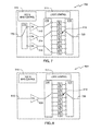
- FIG. 1C is a block diagram of an exemplary wireless communication system of a mobile device showing an RF Front End containing the World Band Amplifiers or World Band RFFE Modules disclosed herein.
- FIG. 4 is a block diagram illustrating a World Band RF Front End (RFFE) Module that operates in the 698-915 MHz, 1.7-2.1 GHz, 2.3 to 2.7 GHz and 3.3 to 3.8 GHz ranges.
- RFFE World Band RF Front End
- FIG. 10 is a block diagram illustrating an embodiment of the World Band RFFE Module which features mode control for linear and saturated operation.
- FIG. 13 is an exploded view of a multichip module which illustrates a typical construction of a World Band RFFE Module.
- FIG. 4 discloses the World Band RFFE Module 400 and method which is an enhanced version of the World Band Power Amplifier 300 of FIG. 3 which also incorporates a plurality of filters 410 which are integrated into the same package as the power amplifiers ( 302 , 304 , and 306 ), switch module 318 , Vcc & Bias Control circuit 310 and Logic Control 311 .
- the World Band RFFE Module 400 can be used in a transmitter/receiver front end system and configured as disclosed in FIG. 1E .
- the DC/DC converter 1240 a can be integrated inside the World Band RFFE Module 1200 or can be a device external to the World Band RFFE Module 1200 .
- Reference numeral 1250 indicates a circuit which can have linear and saturated mode control and power amplifier protection circuit.
- the World Band RFFE Module 1200 can be used in a transmitter/receiver front end system and configured as disclosed in FIG. 1E .
Abstract
The present disclosure relates to a World Band Radio Frequency Power Amplifier and a World Band Radio Frequency Front End Module. The World Band Power Amplifier can contain at least one broadband power amplifier connected to a switch which can direct an RF input signal to a plurality of transmission paths, each transmission path configured for a different frequency. The World Band RFFE Module is more integrated version of the World Band Power Amplifier that can contain broadband RF PA(s), switches, logic controls, filters, duplexers and other active and passive components. The module may also include a thermal protection system capable of effecting operation of the broadband power amplifier.
Description
This application is a continuation-in-part of U.S. patent application Ser. No. 14/930,632, filed Nov. 2, 2015, which claims the benefit of U.S. patent application Ser. No. 13/918,964, filed Jun. 16, 2013, which claims the benefit of U.S. Provisional Patent Application Ser. No. 61/766,889, filed Feb. 20, 2013; the aforementioned applications being incorporated by reference in their entirety for all purposes.
The present disclosure relates generally to mobile devices and, in particular, in one or more embodiments, the present disclosure relates to amplifiers and front end modules capable of communicating in a plurality of frequency bands and accompanying methods thereof.
Radio frequency (RF) transmission of an electrical signal requires corresponding power amplification for the intended transmission. RF signals typically have a frequency spectrum that can range from several Megahertz (MHZ) to tens of Gigahertz (GHZ) and higher. A major component of the cellular phone is the RF power amplifier. A linear RF power amplifier (PA) is conventionally in the form of a semiconductor Monolithic Microwave Integrated Circuit (MMIC) and can be made using Gallium Arsenide (GaAs), Silicon Germanium (SiGe), Complementary Metal-Oxide-Semiconductor (CMOS), Silicon on Insulator (SOI) and the like. The RF PA and other active and passive components, such as baseband, transceiver, filters, switches, are typically assembled on a printed circuit board (PCB). With the proliferation and introduction of new wireless communication standards (Long Term Evolution (LTE)/Long Term Evolution-Advanced (LTE-A), Super Wi-Fi, etc.) and new communication frequency bands (B40, B41, B17, B12, etc.), wireless communication devices (phones, personal digital assistants (PDA's), tablets, laptops, and the like) must be capable of accessing wireless services through multiple standards and multiple frequency bands.
In current wireless device designs that support multiple frequencies and multiple wireless standards the cost, the size and the complexity of wireless devices can be problematic.
As aspects of embodiments disclosed herein include: an integrated module for use in a radio frequency (RF) front end system comprising: a first broadband power amplifier configured to amplify an RF signal; and a thermal protection system capable of effecting operation of the broadband power amplifier.
Further aspects of embodiments disclosed herein include: an integrated module for use in a radio frequency (RF) front end system comprising: a first broadband power amplifier configured to amplify an RF signal; and a voltage regulator coupled to a temperature sensor and a Vcc and Bias Controller, wherein the voltage regulator is configured to bias the Vcc and Bias Controller to enable and disable operation of the broadband power amplifier based on the temperature sensor output.
Further aspects of embodiments disclosed herein include a method of protecting a broadband power amplifier in an integrated module by disabling operation of amplifier at a predetermined temperature: amplifying an radio frequency (RF) signal using the broadband power amplifier; and disabling operation of the amplifier at a predetermined temperature.
The present disclosure provides a detailed description of a World Band RF Power Amplifier (“World Band Power Amplifier”) and a World Band Radio Frequency Front End Module (“World Band RFFE Module”) and accompanying methods thereof. The World Band Power Amplifier can contain at least one broadband power amplifier connected to a switch which can direct an RF input signal to a plurality of transmission paths, each transmission path configured for a different frequency. The World Band RFFE Module is more integrated version of the World Band Power Amplifier that can contain broadband RF PA(s), switches, logic controls, filters, duplexers and other active and passive components. As new wireless frequency bands and wireless standards are being introduced and are being combined with previous wireless bands in a single device, the RF complexity and cost inside mobile devices is becoming greater while the devices are becoming smaller and cheaper. Portable devices such as laptop personal computers, tablets, and cellular phones with wireless communication capability are being developed with multiple bands and multiple standards in ever decreasing size and complexity for convenience of use. Correspondingly, the electrical components thereof must also decrease in size while covering a plurality of bands and providing effective radio transmission performance. However, the substantially high RF complexity associated with wireless RF systems increases the difficulty of miniaturization of the transmission components. For example, each band supported by the communication device would require a separate RF PA and in some cases each standard would require an additional PA's which in turn raises the overall cost. The World Band Power Amplifier and World Band RFFE Module disclosed herein solves this problem by introducing broadband amplifiers that can cover multiple bands (e.g., 698 MHz to 3.8 GHz) and multiple standards (e.g., 2G, 3G, 4G, etc.) and can contain other passive and active components such as switches, filters and/or duplexers to reduce the overall size of the RF front end.
In an alternative embodiment to module 2400, the power amplifier 314 may be redundant to power amplifier 312. When the temperature sensor determines that the temperature in the module as reached a certain threshold value, power amplifier 312 may be shut off and power amplifier 314 will take over operation until (and if) power amplifier 312 is able to be activated again.
Although FIGS. 22-25 show only one temperature sensor 2208, each of the embodiments could have a plurality of temperature sensors coupled to the voltage regulator. In some embodiments, each power amplifier would have its own temperature sensor monitoring the environment around that particular power amplifier.
In this disclosure, devices that are described as in “communication” with each other or “coupled” to each other need not be in continuous communication with each other or in direct physical contact, unless expressly specified otherwise. On the contrary, such devices need only transmit to each other as necessary or desirable, and may actually refrain from exchanging data most of the time. For example, a machine in communication with or coupled with another machine via the Internet may not transmit data to the other machine for long period of time (e.g. weeks at a time). In addition, devices that are in communication with or coupled with each other may communicate directly or indirectly through one or more intermediaries.
Accompanying each of the embodiments disclosed herein is an associated method. Although process (or method) steps may be described or claimed in a particular sequential order, such processes may be configured to work in different orders. In other words, any sequence or order of steps that may be explicitly described or claimed does not necessarily indicate a requirement that the steps be performed in that order unless specifically indicated. Further, some steps may be performed simultaneously despite being described or implied as occurring non-simultaneously (e.g., because one step is described after the other step) unless specifically indicated. Moreover, the illustration of a process by its depiction in a drawing does not imply that the illustrated process is exclusive of other variations and modifications thereto, does not imply that the illustrated process or any of its steps are necessary to the embodiment(s), and does not imply that the illustrated process is preferred.
Further, the foregoing description and embodiments have been presented for purposes of illustration and description and are not intended to be exhaustive or to limit the embodiments in any sense to the precise form disclosed. Many modifications and variations are possible in light of the above teaching. The embodiments were chosen and described to best explain the principles of the disclosure and its practical application to thereby enable others skilled in the art to best use the various embodiments disclosed herein and with various modifications suited to the particular use contemplated. Also, particular aspects or features of the following disclosure may be described with reference to one or more particular embodiments and/or drawings, it should be understood that such features are not limited to usage in the one or more particular embodiments or drawings with reference to which they are described, unless expressly specified otherwise. The functionality and/or the features of the embodiments that are described may be alternatively embodied by one or more other devices which are described but are not explicitly described as having such functionality/features. The actual scope of the invention is to be defined by the following claims.
Claims (8)
1. A method of protecting a first broadband power amplifier in an integrated broadband power amplifier module by disabling operation of the first broadband power amplifier at a predetermined temperature:
amplifying a first radio frequency (RF) signal using the first broadband power amplifier;
sensing the temperature inside the broadband power amplifier module using a first temperature sensor;
enabling and disabling operation of the first broadband power amplifier based on the output of the first temperature sensor; and
a second broadband power amplifier capable of amplifying a second RF signal;
a second temperature sensor output capable of effecting operation of the second broadband amplifier; and
wherein the second broadband amplifier operates when the first broadband amplifier is disabled.
2. The method of claim 1 , wherein the first broadband power amplifier and the temperature sensor are in a single die.
3. The method of claim 1 , further comprising:
coupling the first RF signal through a first switch module to one of a plurality of transmission paths wherein each of said transmission paths are configured to transmit a different frequency band.
4. The module of claim 1 , wherein the first broadband amplifier operates in the millimeter wave band.
5. The module of claim 1 , wherein the first broadband power amplifier in the centimeter wave band.
6. The module of claim 1 , wherein the first broadband power amplifier operates in the approximately 17 GHz to 100 GHz range.
7. The module of claim 1 , wherein the first broadband power amplifier operates in the approximately 2.1 GHz to 7 GHz range.
8. The method of claim 1 , further comprising:
effecting operation of the second broadband power amplifier through a second temperature sensor.
Priority Applications (2)
| Application Number | Priority Date | Filing Date | Title |
|---|---|---|---|
| US15/369,856 US10027287B1 (en) | 2013-02-20 | 2016-12-05 | World band frequency front end module, system and method thereof |
| US16/521,524 US10643962B1 (en) | 2013-02-20 | 2019-07-24 | World band radio frequency front end module, system and method of power sensing thereof |
Applications Claiming Priority (4)
| Application Number | Priority Date | Filing Date | Title |
|---|---|---|---|
| US201361766889P | 2013-02-20 | 2013-02-20 | |
| US13/918,964 US9178555B2 (en) | 2013-02-20 | 2013-06-16 | World band radio frequency front end module, system and method thereof |
| US14/930,632 US9515615B2 (en) | 2013-02-20 | 2015-11-02 | World band radio frequency front end module, system and method thereof |
| US15/369,856 US10027287B1 (en) | 2013-02-20 | 2016-12-05 | World band frequency front end module, system and method thereof |
Related Parent Applications (1)
| Application Number | Title | Priority Date | Filing Date |
|---|---|---|---|
| US14/930,632 Continuation-In-Part US9515615B2 (en) | 2013-02-20 | 2015-11-02 | World band radio frequency front end module, system and method thereof |
Related Child Applications (1)
| Application Number | Title | Priority Date | Filing Date |
|---|---|---|---|
| US201816036929A Continuation-In-Part | 2013-02-20 | 2018-07-16 |
Publications (1)
| Publication Number | Publication Date |
|---|---|
| US10027287B1 true US10027287B1 (en) | 2018-07-17 |
Family
ID=62837298
Family Applications (1)
| Application Number | Title | Priority Date | Filing Date |
|---|---|---|---|
| US15/369,856 Active US10027287B1 (en) | 2013-02-20 | 2016-12-05 | World band frequency front end module, system and method thereof |
Country Status (1)
| Country | Link |
|---|---|
| US (1) | US10027287B1 (en) |
Cited By (11)
| Publication number | Priority date | Publication date | Assignee | Title |
|---|---|---|---|---|
| US20190222238A1 (en) * | 2016-06-25 | 2019-07-18 | Vanchip (Tianjin) Technology Co., Ltd. | Radio frequency front-end transmission method and transmission module, chip, and communications terminal |
| US20190326940A1 (en) * | 2016-04-09 | 2019-10-24 | Skyworks Solutions, Inc. | Multiplexing architectures for wireless applications |
| US10643962B1 (en) * | 2013-02-20 | 2020-05-05 | Micro Mobio Corporation | World band radio frequency front end module, system and method of power sensing thereof |
| US10700717B1 (en) * | 2019-03-19 | 2020-06-30 | Samsung Electro-Mechanics Co., Ltd. | Band selection switch circuit and amplifier |
| US20200211998A1 (en) * | 2018-12-28 | 2020-07-02 | Murata Manufacturing Co., Ltd. | Radio-frequency module and communication device |
| US11038546B2 (en) | 2019-09-02 | 2021-06-15 | Samsung Electronics Co., Ltd. | Electronic device including a temperature sensor connected to a power amplifier and a controller to control an input power based on a temperature of the power amplifier detected by the temperature sensor |
| US20210344327A1 (en) * | 2016-12-21 | 2021-11-04 | Skyworks Solutions, Inc. | Acoustic wave filter with temperature sensor |
| EP3906615A4 (en) * | 2019-03-29 | 2022-03-09 | Samsung Electronics Co., Ltd. | Voltage protection circuit to prevent power amplifier burnout, and electronic device having the same |
| WO2022055164A1 (en) * | 2020-09-11 | 2022-03-17 | 삼성전자 주식회사 | Electronic device for operating antenna module and method for controlling same |
| US11476824B2 (en) * | 2020-07-09 | 2022-10-18 | Hewlett Packard Enterprise Development Lp | Selective filtering for continuous 5 GHz and 6 GHz operation of a network device |
| EP4283866A1 (en) * | 2022-05-26 | 2023-11-29 | Qorvo US, Inc. | Power protection loop for amplifier chain elements |
Citations (22)
| Publication number | Priority date | Publication date | Assignee | Title |
|---|---|---|---|---|
| US5973557A (en) | 1996-10-18 | 1999-10-26 | Matsushita Electric Industrial Co., Ltd. | High efficiency linear power amplifier of plural frequency bands and high efficiency power amplifier |
| US20040232982A1 (en) | 2002-07-19 | 2004-11-25 | Ikuroh Ichitsubo | RF front-end module for wireless communication devices |
| US20090180403A1 (en) | 2008-01-11 | 2009-07-16 | Bogdan Tudosoiu | Multi-band and multi-mode radio frequency front-end module architecture |
| US20100091752A1 (en) | 2006-12-19 | 2010-04-15 | Shigeru Kemmochi | High frequency circuit, high frequency component and communication device |
| US20100156537A1 (en) * | 2006-05-17 | 2010-06-24 | Dishop Steven M | Solid-state rf power amplifier for radio transmitters |
| US20100291888A1 (en) | 2009-05-12 | 2010-11-18 | Qualcomm Incorporated | Multi-mode multi-band power amplifier module |
| US20110222443A1 (en) | 2010-03-12 | 2011-09-15 | Rf Micro Devices, Inc. | Lte-advanced (4g) front end radio architecture |
| US20120049953A1 (en) | 2010-08-25 | 2012-03-01 | Rf Micro Devices, Inc. | Multi-mode/multi-band power management system |
| US20120313710A1 (en) * | 2011-06-07 | 2012-12-13 | Hull Jr William P | Performance optimization of power amplifier |
| US20130051284A1 (en) | 2011-08-23 | 2013-02-28 | Rf Micro Devices, Inc. | Carrier aggregation radio system |
| US8441320B2 (en) * | 2010-12-13 | 2013-05-14 | Marvell World Trade Ltd. | Cancelation of gain change due to amplifier self-heating |
| US20130328723A1 (en) | 2008-08-14 | 2013-12-12 | Theodore S. Rappaport | Steerable Antenna Device |
| US20130336181A1 (en) | 2012-06-18 | 2013-12-19 | Rf Micro Devices, Inc. | Dual antenna integrated carrier aggregation front end solution |
| US20140002187A1 (en) * | 2012-06-28 | 2014-01-02 | Skyworks Solutions, Inc. | Integrated rf front end system |
| US20140015603A1 (en) | 2012-07-13 | 2014-01-16 | Amalfi Semiconductor, Inc. | Multi-Band/Multi-Mode Power Amplifier with Signal Path Hardware Sharing |
| US20140024322A1 (en) | 2012-07-18 | 2014-01-23 | Rf Micro Devices, Inc. | Radio front end having reduced diversity switch linearity requirement |
| US8699974B2 (en) | 2011-08-24 | 2014-04-15 | Aviacomm Inc. | Wideband transmitter front-end |
| US20140169243A1 (en) | 2012-12-18 | 2014-06-19 | Rf Micro Devices, Inc. | Mobile communication circuitry for three or more antennas |
| US20140333382A1 (en) * | 2010-03-25 | 2014-11-13 | Llyod L. Lautzenhiser | Method and system for providing automatic gate bias and bias sequencing for field effect transistors |
| US20140368277A1 (en) * | 2013-06-13 | 2014-12-18 | Advanced Semiconductor Engineering Inc. | Radio frequency power amplifier and electronic system |
| US20150050901A1 (en) | 2012-12-19 | 2015-02-19 | Qualcomm Incorporated | Multi-mode multi-band power amplifiers |
| US9712261B2 (en) * | 2013-08-15 | 2017-07-18 | Silicon Laboratories Inc. | Apparatus and method of background temperature calibration |
-
2016
- 2016-12-05 US US15/369,856 patent/US10027287B1/en active Active
Patent Citations (22)
| Publication number | Priority date | Publication date | Assignee | Title |
|---|---|---|---|---|
| US5973557A (en) | 1996-10-18 | 1999-10-26 | Matsushita Electric Industrial Co., Ltd. | High efficiency linear power amplifier of plural frequency bands and high efficiency power amplifier |
| US20040232982A1 (en) | 2002-07-19 | 2004-11-25 | Ikuroh Ichitsubo | RF front-end module for wireless communication devices |
| US20100156537A1 (en) * | 2006-05-17 | 2010-06-24 | Dishop Steven M | Solid-state rf power amplifier for radio transmitters |
| US20100091752A1 (en) | 2006-12-19 | 2010-04-15 | Shigeru Kemmochi | High frequency circuit, high frequency component and communication device |
| US20090180403A1 (en) | 2008-01-11 | 2009-07-16 | Bogdan Tudosoiu | Multi-band and multi-mode radio frequency front-end module architecture |
| US20130328723A1 (en) | 2008-08-14 | 2013-12-12 | Theodore S. Rappaport | Steerable Antenna Device |
| US20100291888A1 (en) | 2009-05-12 | 2010-11-18 | Qualcomm Incorporated | Multi-mode multi-band power amplifier module |
| US20110222443A1 (en) | 2010-03-12 | 2011-09-15 | Rf Micro Devices, Inc. | Lte-advanced (4g) front end radio architecture |
| US20140333382A1 (en) * | 2010-03-25 | 2014-11-13 | Llyod L. Lautzenhiser | Method and system for providing automatic gate bias and bias sequencing for field effect transistors |
| US20120049953A1 (en) | 2010-08-25 | 2012-03-01 | Rf Micro Devices, Inc. | Multi-mode/multi-band power management system |
| US8441320B2 (en) * | 2010-12-13 | 2013-05-14 | Marvell World Trade Ltd. | Cancelation of gain change due to amplifier self-heating |
| US20120313710A1 (en) * | 2011-06-07 | 2012-12-13 | Hull Jr William P | Performance optimization of power amplifier |
| US20130051284A1 (en) | 2011-08-23 | 2013-02-28 | Rf Micro Devices, Inc. | Carrier aggregation radio system |
| US8699974B2 (en) | 2011-08-24 | 2014-04-15 | Aviacomm Inc. | Wideband transmitter front-end |
| US20130336181A1 (en) | 2012-06-18 | 2013-12-19 | Rf Micro Devices, Inc. | Dual antenna integrated carrier aggregation front end solution |
| US20140002187A1 (en) * | 2012-06-28 | 2014-01-02 | Skyworks Solutions, Inc. | Integrated rf front end system |
| US20140015603A1 (en) | 2012-07-13 | 2014-01-16 | Amalfi Semiconductor, Inc. | Multi-Band/Multi-Mode Power Amplifier with Signal Path Hardware Sharing |
| US20140024322A1 (en) | 2012-07-18 | 2014-01-23 | Rf Micro Devices, Inc. | Radio front end having reduced diversity switch linearity requirement |
| US20140169243A1 (en) | 2012-12-18 | 2014-06-19 | Rf Micro Devices, Inc. | Mobile communication circuitry for three or more antennas |
| US20150050901A1 (en) | 2012-12-19 | 2015-02-19 | Qualcomm Incorporated | Multi-mode multi-band power amplifiers |
| US20140368277A1 (en) * | 2013-06-13 | 2014-12-18 | Advanced Semiconductor Engineering Inc. | Radio frequency power amplifier and electronic system |
| US9712261B2 (en) * | 2013-08-15 | 2017-07-18 | Silicon Laboratories Inc. | Apparatus and method of background temperature calibration |
Cited By (13)
| Publication number | Priority date | Publication date | Assignee | Title |
|---|---|---|---|---|
| US10643962B1 (en) * | 2013-02-20 | 2020-05-05 | Micro Mobio Corporation | World band radio frequency front end module, system and method of power sensing thereof |
| US20190326940A1 (en) * | 2016-04-09 | 2019-10-24 | Skyworks Solutions, Inc. | Multiplexing architectures for wireless applications |
| US20190222238A1 (en) * | 2016-06-25 | 2019-07-18 | Vanchip (Tianjin) Technology Co., Ltd. | Radio frequency front-end transmission method and transmission module, chip, and communications terminal |
| US20210344327A1 (en) * | 2016-12-21 | 2021-11-04 | Skyworks Solutions, Inc. | Acoustic wave filter with temperature sensor |
| US11476226B2 (en) * | 2018-12-28 | 2022-10-18 | Murata Manufacturing Co., Ltd. | Radio-frequency module and communication device |
| US20200211998A1 (en) * | 2018-12-28 | 2020-07-02 | Murata Manufacturing Co., Ltd. | Radio-frequency module and communication device |
| US10700717B1 (en) * | 2019-03-19 | 2020-06-30 | Samsung Electro-Mechanics Co., Ltd. | Band selection switch circuit and amplifier |
| EP3906615A4 (en) * | 2019-03-29 | 2022-03-09 | Samsung Electronics Co., Ltd. | Voltage protection circuit to prevent power amplifier burnout, and electronic device having the same |
| US11843398B2 (en) | 2019-03-29 | 2023-12-12 | Samsung Electronics Co., Ltd | Voltage protection circuit to prevent power amplifier burnout, and electronic device having the same |
| US11038546B2 (en) | 2019-09-02 | 2021-06-15 | Samsung Electronics Co., Ltd. | Electronic device including a temperature sensor connected to a power amplifier and a controller to control an input power based on a temperature of the power amplifier detected by the temperature sensor |
| US11476824B2 (en) * | 2020-07-09 | 2022-10-18 | Hewlett Packard Enterprise Development Lp | Selective filtering for continuous 5 GHz and 6 GHz operation of a network device |
| WO2022055164A1 (en) * | 2020-09-11 | 2022-03-17 | 삼성전자 주식회사 | Electronic device for operating antenna module and method for controlling same |
| EP4283866A1 (en) * | 2022-05-26 | 2023-11-29 | Qorvo US, Inc. | Power protection loop for amplifier chain elements |
Similar Documents
| Publication | Publication Date | Title |
|---|---|---|
| US10027287B1 (en) | World band frequency front end module, system and method thereof | |
| US10643962B1 (en) | World band radio frequency front end module, system and method of power sensing thereof | |
| US9178555B2 (en) | World band radio frequency front end module, system and method thereof | |
| US9515615B2 (en) | World band radio frequency front end module, system and method thereof | |
| KR101788396B1 (en) | Multi-band device with reduced band loading | |
| US11881822B2 (en) | Power amplifier module | |
| US11451248B2 (en) | Front-end systems with a shared back switch | |
| US10461785B2 (en) | Apparatus and methods for front-end systems with reactive loopback | |
| US20180294569A1 (en) | Radio-frequency module with integrated shield layer antenna and integrated cavity-based antenna | |
| CN105099484A (en) | Global frequency range RFFE module and system thereof | |
| US20210152195A1 (en) | Radio frequency module and communication device | |
| US11742337B2 (en) | Radio-frequency module and communication device | |
| US20040201423A1 (en) | Handset radiofrequency front end module in fine pitch quad flat no lead (FQFP-N) package | |
| US20190028137A1 (en) | Radio-frequency (rf) connectors with integrated radio-frequency device | |
| US20210399423A1 (en) | Radio-frequency module with integrated conformal shield antenna | |
| US11418225B2 (en) | Radio frequency module and communication device | |
| US20180294558A1 (en) | Radio-frequency module with integrated conformal shield antenna | |
| KR100519817B1 (en) | Dual band cdma transceiver complex module | |
| KR101119384B1 (en) | Intergrated tramsmission module in the radio transmitter-receiver | |
| Kaho et al. | Quad-band receiver front-end module using SiGe BiCMOS MMICs and LTCC triplexer | |
| US9209507B1 (en) | Monolithic wideband high power termination element |
Legal Events
| Date | Code | Title | Description |
|---|---|---|---|
| STCF | Information on status: patent grant |
Free format text: PATENTED CASE |
|
| FEPP | Fee payment procedure |
Free format text: MAINTENANCE FEE REMINDER MAILED (ORIGINAL EVENT CODE: REM.); ENTITY STATUS OF PATENT OWNER: SMALL ENTITY |
|
| FEPP | Fee payment procedure |
Free format text: SURCHARGE FOR LATE PAYMENT, SMALL ENTITY (ORIGINAL EVENT CODE: M2554); ENTITY STATUS OF PATENT OWNER: SMALL ENTITY |
|
| MAFP | Maintenance fee payment |
Free format text: PAYMENT OF MAINTENANCE FEE, 4TH YR, SMALL ENTITY (ORIGINAL EVENT CODE: M2551); ENTITY STATUS OF PATENT OWNER: SMALL ENTITY Year of fee payment: 4 |