EP2930583A2 - Erzeugungsschaltkreis einer bezugsspannung - Google Patents
Erzeugungsschaltkreis einer bezugsspannung Download PDFInfo
- Publication number
- EP2930583A2 EP2930583A2 EP15160418.8A EP15160418A EP2930583A2 EP 2930583 A2 EP2930583 A2 EP 2930583A2 EP 15160418 A EP15160418 A EP 15160418A EP 2930583 A2 EP2930583 A2 EP 2930583A2
- Authority
- EP
- European Patent Office
- Prior art keywords
- transistor
- current source
- current
- reference voltage
- circuit
- Prior art date
- Legal status (The legal status is an assumption and is not a legal conclusion. Google has not performed a legal analysis and makes no representation as to the accuracy of the status listed.)
- Granted
Links
- 238000005516 engineering process Methods 0.000 description 8
- 239000006185 dispersion Substances 0.000 description 1
- 230000000694 effects Effects 0.000 description 1
- 238000004519 manufacturing process Methods 0.000 description 1
Images


Classifications
-
- G—PHYSICS
- G05—CONTROLLING; REGULATING
- G05F—SYSTEMS FOR REGULATING ELECTRIC OR MAGNETIC VARIABLES
- G05F3/00—Non-retroactive systems for regulating electric variables by using an uncontrolled element, or an uncontrolled combination of elements, such element or such combination having self-regulating properties
- G05F3/02—Regulating voltage or current
- G05F3/08—Regulating voltage or current wherein the variable is DC
- G05F3/10—Regulating voltage or current wherein the variable is DC using uncontrolled devices with non-linear characteristics
- G05F3/16—Regulating voltage or current wherein the variable is DC using uncontrolled devices with non-linear characteristics being semiconductor devices
-
- G—PHYSICS
- G05—CONTROLLING; REGULATING
- G05F—SYSTEMS FOR REGULATING ELECTRIC OR MAGNETIC VARIABLES
- G05F3/00—Non-retroactive systems for regulating electric variables by using an uncontrolled element, or an uncontrolled combination of elements, such element or such combination having self-regulating properties
- G05F3/02—Regulating voltage or current
- G05F3/08—Regulating voltage or current wherein the variable is DC
- G05F3/10—Regulating voltage or current wherein the variable is DC using uncontrolled devices with non-linear characteristics
- G05F3/16—Regulating voltage or current wherein the variable is DC using uncontrolled devices with non-linear characteristics being semiconductor devices
- G05F3/20—Regulating voltage or current wherein the variable is DC using uncontrolled devices with non-linear characteristics being semiconductor devices using diode- transistor combinations
- G05F3/26—Current mirrors
-
- G—PHYSICS
- G05—CONTROLLING; REGULATING
- G05F—SYSTEMS FOR REGULATING ELECTRIC OR MAGNETIC VARIABLES
- G05F3/00—Non-retroactive systems for regulating electric variables by using an uncontrolled element, or an uncontrolled combination of elements, such element or such combination having self-regulating properties
- G05F3/02—Regulating voltage or current
- G05F3/08—Regulating voltage or current wherein the variable is DC
- G05F3/10—Regulating voltage or current wherein the variable is DC using uncontrolled devices with non-linear characteristics
- G05F3/16—Regulating voltage or current wherein the variable is DC using uncontrolled devices with non-linear characteristics being semiconductor devices
- G05F3/20—Regulating voltage or current wherein the variable is DC using uncontrolled devices with non-linear characteristics being semiconductor devices using diode- transistor combinations
- G05F3/26—Current mirrors
- G05F3/267—Current mirrors using both bipolar and field-effect technology
-
- G—PHYSICS
- G05—CONTROLLING; REGULATING
- G05F—SYSTEMS FOR REGULATING ELECTRIC OR MAGNETIC VARIABLES
- G05F3/00—Non-retroactive systems for regulating electric variables by using an uncontrolled element, or an uncontrolled combination of elements, such element or such combination having self-regulating properties
- G05F3/02—Regulating voltage or current
- G05F3/08—Regulating voltage or current wherein the variable is DC
- G05F3/10—Regulating voltage or current wherein the variable is DC using uncontrolled devices with non-linear characteristics
- G05F3/16—Regulating voltage or current wherein the variable is DC using uncontrolled devices with non-linear characteristics being semiconductor devices
- G05F3/20—Regulating voltage or current wherein the variable is DC using uncontrolled devices with non-linear characteristics being semiconductor devices using diode- transistor combinations
- G05F3/30—Regulators using the difference between the base-emitter voltages of two bipolar transistors operating at different current densities
Definitions
- the present application relates to a circuit for generating a reference voltage under a supply voltage of less than 1 V.
- the input of the follower assembly is connected to the collector of the transistor Q1 and its output is connected by a resistor optional R2 at the base of transistor Q2.
- a resistive divider bridge composed of resistors R3 and R4 in series is connected between the output terminal of the follower assembly 3 and the ground GND. The midpoint of this divider bridge is connected to the base of transistor Q1.
- the resistor R4 is connected between the base of the transistor Q1 and the ground GND.
- the current mirror composed of the MOS transistors M1 and M2 causes the two transistors Q1 and Q2 to receive the same collector current.
- V OUT V BE ⁇ 1 * R 4 / R 3 + kT / q * ln p 2
- V BE1 denotes the base-emitter voltage of the transistor Q1
- k denotes the Boltzmann constant
- q denotes the charge of the electron
- T denotes the temperature in Kelvin
- 1 ) denotes the natural logarithm of the ratio. of surface p 2
- the follower assembly 3 is composed of a current source 4 and a MOS transistor M3.
- the gate of the transistor M3 corresponds to the input of the follower assembly 3 and the source of the MOS transistor M3 corresponds to the output of the follower assembly 3.
- the follower assembly sends the voltage present on its input to its output and supplies the current required for the controlling the bases of the transistors Q1 and Q2 and the resistor R4. This circuit has an infinite input impedance, and no current flows in the gate of the MOS transistor M3.
- the base currents of the transistors Q1 and Q2 are equal (thanks to the two transistors M1 and M2 mounted in current mirror).
- Resistor R2 is added to cancel the effect of the base currents on the reference voltage. The compensation will be optimal if the resistance values R2 and R3 are equal.
- V DD V OUT + V BE ⁇ 2 + R ⁇ 2 * I b ⁇ 2 + V 4 , where V OUT is the reference voltage generated by the circuit, V BE2 is the base-emitter voltage of transistor Q2, and V 4 is the voltage drop across the current source 4.
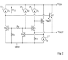
- a resistor R5 is connected between the base of the transistor Q3 and the ground GND.
- a resistor R6 is connected between the collector of transistor Q4 and the base of transistor Q3.
- a bipolar transistor Q7 is connected between the terminal V DD and the emitter of the transistor Q5.
- the base of transistor Q7 is connected to the collector of transistor Q3.
- the point of connection of the emitters of transistors Q5 and Q7 constitutes the output V OUT of the circuit.
- Transistors Q3 and Q5 receive the same collector current I 1 .
- V DD V OUT + V BE ⁇ 7 + V 11 , where V OUT is the reference voltage generated by the circuit, V BE7 is the base-emitter voltage of transistor Q7 and V 11 is the voltage drop across current source 11.
- the supply voltages of the circuits of figures 1 and 2 are greater than or equal to 1 V.
- an embodiment provides a reference voltage generating circuit comprising between first and second terminals for applying a supply voltage: a first current source in series with a first bipolar transistor; a second current source in series with a first resistive element, the connection point between the second current source and the first resistive element being connected to the base of the first bipolar transistor; a third current source in series with a second bipolar transistor, the third current source being in current mirror with the first current source; a second resistive element between the base of the second bipolar transistor and the connection point between the second current source and the first resistive element; and a fourth current source in series with a third resistive element, the connection point between the fourth current source and the third resistive element defining a third terminal providing the reference voltage, the fourth current source being in current mirror with the second source of current.
- a fifth current source is connected between the first terminal and the third terminal, and a fourth resistive element is connected in series with the second bipolar transistor, the fifth current source being in current mirror with the first Power source.
- the current sources are formed of MOS transistors.
- the collector surface of the second bipolar transistor is greater than the collector surface of the first bipolar transistor.
- PMOS transistor will be called P-channel MOS transistors.
- the current mirror composed of transistors M4 and M6 causes transistors Q8 and Q9 to receive equal collector currents I c8 and I c9 .
- the circuit is designed so that the transistor M5 is in saturation mode.
- V DD V BE ⁇ 8 + V M ⁇ 5
- V BE8 is the base-emitter voltage of transistor Q8
- V M5 is the drain-source voltage of transistor M5.
- the base-emitter voltage of a bipolar transistor is of the order of 0.8 V and the drain-source voltage of a saturation MOS transistor is of the order
- the transistor M7 operates in linear mode when the reference voltage V OUT is lower than the voltage V BE8 (0.8 V). For a supply voltage of 0.9 V, it is therefore possible to set the reference voltage V OUT in a range from 0.1 V to 0.8 V.
- V OUT R ⁇ 10 * I M ⁇ 7 , where I M7 is the current in resistor R10. Since the transistors M5 and M7 are mounted in a current mirror, the current I M7 is the copy of the current I M5 .
- V OUT R ⁇ 10 * V BE ⁇ 8 / R ⁇ 8 + 2 * kT / q * R ⁇ 9 * ln p 9
- this circuit can generate a reference voltage V OUT of between 0.1 V and 0.8 V.
- the reference voltage V OUT depends on the base current I b9 of transistor Q9.
- the gain ⁇ varies with the temperature and the manufacturing dispersions. Currents I c8 and I c9 vary accordingly.
- the voltage V BE8 varies according to the current Ic8.
- the voltage V OUT depends on V BE8 .
- the variation of the gain ⁇ of the transistor Q9 therefore degrades the accuracy of the reference voltage V OUT generated.
- the voltage V OUT varies by approximately 2%.
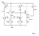
- the figure 4 illustrates another exemplary embodiment of a reference voltage generation circuit presenting the advantages of the embodiment of the figure 3 while avoiding the possible variation of V OUT with the gain ⁇ .
- This circuit includes the elements of the circuit of the figure 3 designated by the same references.
- a resistor R11 is placed between the emitter of transistor Q9 and the ground GND and a PMOS transistor M10 is connected between the supply voltage V DD and the drain of the transistor M7.
- the source of the transistor M10 is connected to the voltage V DD .
- the transistor M10 is mounted in current mirror with the transistors M4 and M6.
- V DD V BE ⁇ 8 + V M ⁇ 5 ,
- I R10 is the current in resistor R10 and I M10 is the drain current of transistor M10.
- the transistors M4, M6 and M10 being mounted in current mirror, the currents I c8 , I c9 and I M10 are equal. Since the transistors M5 and M7 are mounted in a current mirror, the currents I M5 and I M7 are equal.
- V E .DELTA.V BE - R ⁇ 9 * I b ⁇ 9
- I vs ⁇ 9 .DELTA.V BE / R ⁇ 11 - Ib ⁇ 9 * 1 + R ⁇ 9 / R ⁇ 11 .
- I R ⁇ 10 V BE ⁇ 8 / R ⁇ 8 + 2 * I b ⁇ 9 + .DELTA.V BE / R ⁇ 11 - Ib ⁇ 9 * 1 + R ⁇ 9 / R ⁇ 11 .
- I R10 V BE ⁇ 8 / R ⁇ 8 + .DELTA.V BE / R ⁇ 11
- V OUT R ⁇ 10 * V BE ⁇ 8 / R ⁇ 8 + kT / q * R ⁇ 9 * ln p 9
- the current I c9 no longer depends on the gain ⁇ , unlike the case of the circuit of the figure 3 .
- the voltage V BE8 is no longer affected by the variation of the gain ⁇ and since the voltage V OUT depends on V BE8 , the accuracy of the voltage V OUT is no longer affected by the gain ⁇ .
- An advantage of such a circuit is that any gain variation ⁇ of the transistor Q9 does not affect the accuracy of the reference voltage VOUT.
- resistance has been used here to denote the elements R1 to R11, it will be noted that these elements may consist of any resistive element such as a resistance-connected MOS transistor.
- the values of the resistances can be between 1 and 100 k ⁇ , for example 50 k ⁇ .
Landscapes
- Engineering & Computer Science (AREA)
- Physics & Mathematics (AREA)
- Microelectronics & Electronic Packaging (AREA)
- Nonlinear Science (AREA)
- Electromagnetism (AREA)
- General Physics & Mathematics (AREA)
- Radar, Positioning & Navigation (AREA)
- Automation & Control Theory (AREA)
- Power Engineering (AREA)
- Control Of Electrical Variables (AREA)
Applications Claiming Priority (1)
| Application Number | Priority Date | Filing Date | Title |
|---|---|---|---|
| FR1453014A FR3019660A1 (fr) | 2014-04-04 | 2014-04-04 | Circuit de generation d'une tension de reference |
Publications (3)
| Publication Number | Publication Date |
|---|---|
| EP2930583A2 true EP2930583A2 (de) | 2015-10-14 |
| EP2930583A3 EP2930583A3 (de) | 2015-12-16 |
| EP2930583B1 EP2930583B1 (de) | 2019-01-30 |
Family
ID=51225684
Family Applications (1)
| Application Number | Title | Priority Date | Filing Date |
|---|---|---|---|
| EP15160418.8A Active EP2930583B1 (de) | 2014-04-04 | 2015-03-23 | Erzeugungsschaltkreis einer bezugsspannung |
Country Status (3)
| Country | Link |
|---|---|
| US (1) | US9588538B2 (de) |
| EP (1) | EP2930583B1 (de) |
| FR (1) | FR3019660A1 (de) |
Citations (2)
| Publication number | Priority date | Publication date | Assignee | Title |
|---|---|---|---|---|
| US7408400B1 (en) | 2006-08-16 | 2008-08-05 | National Semiconductor Corporation | System and method for providing a low voltage bandgap reference circuit |
| FR2969328A1 (fr) | 2010-12-17 | 2012-06-22 | St Microelectronics Sa | Circuit de generation d'une tension de reference sous une faible tension d'alimentation |
Family Cites Families (9)
| Publication number | Priority date | Publication date | Assignee | Title |
|---|---|---|---|---|
| US4157493A (en) * | 1977-09-02 | 1979-06-05 | National Semiconductor Corporation | Delta VBE generator circuit |
| US4590419A (en) * | 1984-11-05 | 1986-05-20 | General Motors Corporation | Circuit for generating a temperature-stabilized reference voltage |
| US5349286A (en) * | 1993-06-18 | 1994-09-20 | Texas Instruments Incorporated | Compensation for low gain bipolar transistors in voltage and current reference circuits |
| JP3586073B2 (ja) | 1997-07-29 | 2004-11-10 | 株式会社東芝 | 基準電圧発生回路 |
| US6002243A (en) * | 1998-09-02 | 1999-12-14 | Texas Instruments Incorporated | MOS circuit stabilization of bipolar current mirror collector voltages |
| WO2006038057A1 (en) * | 2004-10-08 | 2006-04-13 | Freescale Semiconductor, Inc | Reference circuit |
| JP2009098802A (ja) | 2007-10-15 | 2009-05-07 | Toshiba Corp | 基準電圧発生回路 |
| TWI337694B (en) * | 2007-12-06 | 2011-02-21 | Ind Tech Res Inst | Bandgap reference circuit |
| TWI399631B (zh) * | 2010-01-12 | 2013-06-21 | Richtek Technology Corp | 可快速啟動的低電壓能隙參考電壓產生器 |
-
2014
- 2014-04-04 FR FR1453014A patent/FR3019660A1/fr active Pending
-
2015
- 2015-03-23 EP EP15160418.8A patent/EP2930583B1/de active Active
- 2015-03-31 US US14/675,309 patent/US9588538B2/en active Active
Patent Citations (2)
| Publication number | Priority date | Publication date | Assignee | Title |
|---|---|---|---|---|
| US7408400B1 (en) | 2006-08-16 | 2008-08-05 | National Semiconductor Corporation | System and method for providing a low voltage bandgap reference circuit |
| FR2969328A1 (fr) | 2010-12-17 | 2012-06-22 | St Microelectronics Sa | Circuit de generation d'une tension de reference sous une faible tension d'alimentation |
Also Published As
| Publication number | Publication date |
|---|---|
| EP2930583A3 (de) | 2015-12-16 |
| FR3019660A1 (fr) | 2015-10-09 |
| US20150286238A1 (en) | 2015-10-08 |
| EP2930583B1 (de) | 2019-01-30 |
| US9588538B2 (en) | 2017-03-07 |
Similar Documents
| Publication | Publication Date | Title |
|---|---|---|
| FR2912013A1 (fr) | Dispositif de generation de courant de polarisation ayant un coefficient de temperature ajustable. | |
| US9092044B2 (en) | Low voltage, low power bandgap circuit | |
| TWI694321B (zh) | 提供可調恆定電流之電流電路 | |
| TWI859269B (zh) | 參考電壓電路 | |
| DE19804747A1 (de) | Bandabstandsbezugsschaltung und Verfahren | |
| TW200941184A (en) | Operational amplifier, temperature-independent system and bandgap reference circuit | |
| JP2008516328A (ja) | 基準回路 | |
| US20140247034A1 (en) | Low supply voltage bandgap reference circuit and method | |
| US7589580B2 (en) | Reference current generating method and current reference circuit | |
| FR3071318A1 (fr) | Detection de perturbations d'une tension continue | |
| US6388507B1 (en) | Voltage to current converter with variation-free MOS resistor | |
| EP2067090B1 (de) | Spannungsreferenz-elektronikschaltung | |
| JP2004086750A (ja) | バンドギャップ回路 | |
| CN101213740A (zh) | 与温度无关的放大器偏移修整电路 | |
| CN100464275C (zh) | 调整bgr电路的方法及bgr电路 | |
| JP2021125091A (ja) | 基準電圧回路 | |
| EP2930583B1 (de) | Erzeugungsschaltkreis einer bezugsspannung | |
| US6771055B1 (en) | Bandgap using lateral PNPs | |
| US7253677B1 (en) | Bias circuit for compensating fluctuation of supply voltage | |
| US20120153997A1 (en) | Circuit for Generating a Reference Voltage Under a Low Power Supply Voltage | |
| TW202046041A (zh) | 電壓產生器 | |
| US5864230A (en) | Variation-compensated bias current generator | |
| JP4517062B2 (ja) | 定電圧発生回路 | |
| JPH11194841A (ja) | フローティング基準電圧を用いたシャント電圧レギュレータ | |
| CN116069100A (zh) | 带隙基准电路、芯片及电子设备 |
Legal Events
| Date | Code | Title | Description |
|---|---|---|---|
| PUAI | Public reference made under article 153(3) epc to a published international application that has entered the european phase |
Free format text: ORIGINAL CODE: 0009012 |
|
| 17P | Request for examination filed |
Effective date: 20150323 |
|
| AK | Designated contracting states |
Kind code of ref document: A2 Designated state(s): AL AT BE BG CH CY CZ DE DK EE ES FI FR GB GR HR HU IE IS IT LI LT LU LV MC MK MT NL NO PL PT RO RS SE SI SK SM TR |
|
| AX | Request for extension of the european patent |
Extension state: BA ME |
|
| PUAL | Search report despatched |
Free format text: ORIGINAL CODE: 0009013 |
|
| AK | Designated contracting states |
Kind code of ref document: A3 Designated state(s): AL AT BE BG CH CY CZ DE DK EE ES FI FR GB GR HR HU IE IS IT LI LT LU LV MC MK MT NL NO PL PT RO RS SE SI SK SM TR |
|
| AX | Request for extension of the european patent |
Extension state: BA ME |
|
| RIC1 | Information provided on ipc code assigned before grant |
Ipc: G05F 3/30 20060101AFI20151106BHEP |
|
| REG | Reference to a national code |
Ref country code: DE Ref legal event code: R079 Ref document number: 602015023864 Country of ref document: DE Free format text: PREVIOUS MAIN CLASS: G05F0003300000 Ipc: G05F0003260000 |
|
| GRAP | Despatch of communication of intention to grant a patent |
Free format text: ORIGINAL CODE: EPIDOSNIGR1 |
|
| STAA | Information on the status of an ep patent application or granted ep patent |
Free format text: STATUS: GRANT OF PATENT IS INTENDED |
|
| RIC1 | Information provided on ipc code assigned before grant |
Ipc: G05F 3/30 20060101ALI20180925BHEP Ipc: G05F 3/26 20060101AFI20180925BHEP |
|
| INTG | Intention to grant announced |
Effective date: 20181017 |
|
| GRAS | Grant fee paid |
Free format text: ORIGINAL CODE: EPIDOSNIGR3 |
|
| GRAA | (expected) grant |
Free format text: ORIGINAL CODE: 0009210 |
|
| STAA | Information on the status of an ep patent application or granted ep patent |
Free format text: STATUS: THE PATENT HAS BEEN GRANTED |
|
| AK | Designated contracting states |
Kind code of ref document: B1 Designated state(s): AL AT BE BG CH CY CZ DE DK EE ES FI FR GB GR HR HU IE IS IT LI LT LU LV MC MK MT NL NO PL PT RO RS SE SI SK SM TR |
|
| REG | Reference to a national code |
Ref country code: GB Ref legal event code: FG4D Free format text: NOT ENGLISH |
|
| REG | Reference to a national code |
Ref country code: CH Ref legal event code: EP |
|
| REG | Reference to a national code |
Ref country code: AT Ref legal event code: REF Ref document number: 1093761 Country of ref document: AT Kind code of ref document: T Effective date: 20190215 |
|
| REG | Reference to a national code |
Ref country code: IE Ref legal event code: FG4D Free format text: LANGUAGE OF EP DOCUMENT: FRENCH |
|
| REG | Reference to a national code |
Ref country code: DE Ref legal event code: R096 Ref document number: 602015023864 Country of ref document: DE |
|
| REG | Reference to a national code |
Ref country code: LT Ref legal event code: MG4D |
|
| REG | Reference to a national code |
Ref country code: NL Ref legal event code: MP Effective date: 20190130 |
|
| PG25 | Lapsed in a contracting state [announced via postgrant information from national office to epo] |
Ref country code: PL Free format text: LAPSE BECAUSE OF FAILURE TO SUBMIT A TRANSLATION OF THE DESCRIPTION OR TO PAY THE FEE WITHIN THE PRESCRIBED TIME-LIMIT Effective date: 20190130 Ref country code: LT Free format text: LAPSE BECAUSE OF FAILURE TO SUBMIT A TRANSLATION OF THE DESCRIPTION OR TO PAY THE FEE WITHIN THE PRESCRIBED TIME-LIMIT Effective date: 20190130 Ref country code: FI Free format text: LAPSE BECAUSE OF FAILURE TO SUBMIT A TRANSLATION OF THE DESCRIPTION OR TO PAY THE FEE WITHIN THE PRESCRIBED TIME-LIMIT Effective date: 20190130 Ref country code: NO Free format text: LAPSE BECAUSE OF FAILURE TO SUBMIT A TRANSLATION OF THE DESCRIPTION OR TO PAY THE FEE WITHIN THE PRESCRIBED TIME-LIMIT Effective date: 20190430 Ref country code: PT Free format text: LAPSE BECAUSE OF FAILURE TO SUBMIT A TRANSLATION OF THE DESCRIPTION OR TO PAY THE FEE WITHIN THE PRESCRIBED TIME-LIMIT Effective date: 20190530 Ref country code: SE Free format text: LAPSE BECAUSE OF FAILURE TO SUBMIT A TRANSLATION OF THE DESCRIPTION OR TO PAY THE FEE WITHIN THE PRESCRIBED TIME-LIMIT Effective date: 20190130 Ref country code: ES Free format text: LAPSE BECAUSE OF FAILURE TO SUBMIT A TRANSLATION OF THE DESCRIPTION OR TO PAY THE FEE WITHIN THE PRESCRIBED TIME-LIMIT Effective date: 20190130 Ref country code: NL Free format text: LAPSE BECAUSE OF FAILURE TO SUBMIT A TRANSLATION OF THE DESCRIPTION OR TO PAY THE FEE WITHIN THE PRESCRIBED TIME-LIMIT Effective date: 20190130 |
|
| REG | Reference to a national code |
Ref country code: AT Ref legal event code: MK05 Ref document number: 1093761 Country of ref document: AT Kind code of ref document: T Effective date: 20190130 |
|
| PG25 | Lapsed in a contracting state [announced via postgrant information from national office to epo] |
Ref country code: GR Free format text: LAPSE BECAUSE OF FAILURE TO SUBMIT A TRANSLATION OF THE DESCRIPTION OR TO PAY THE FEE WITHIN THE PRESCRIBED TIME-LIMIT Effective date: 20190501 Ref country code: HR Free format text: LAPSE BECAUSE OF FAILURE TO SUBMIT A TRANSLATION OF THE DESCRIPTION OR TO PAY THE FEE WITHIN THE PRESCRIBED TIME-LIMIT Effective date: 20190130 Ref country code: BG Free format text: LAPSE BECAUSE OF FAILURE TO SUBMIT A TRANSLATION OF THE DESCRIPTION OR TO PAY THE FEE WITHIN THE PRESCRIBED TIME-LIMIT Effective date: 20190430 Ref country code: IS Free format text: LAPSE BECAUSE OF FAILURE TO SUBMIT A TRANSLATION OF THE DESCRIPTION OR TO PAY THE FEE WITHIN THE PRESCRIBED TIME-LIMIT Effective date: 20190530 Ref country code: LV Free format text: LAPSE BECAUSE OF FAILURE TO SUBMIT A TRANSLATION OF THE DESCRIPTION OR TO PAY THE FEE WITHIN THE PRESCRIBED TIME-LIMIT Effective date: 20190130 Ref country code: RS Free format text: LAPSE BECAUSE OF FAILURE TO SUBMIT A TRANSLATION OF THE DESCRIPTION OR TO PAY THE FEE WITHIN THE PRESCRIBED TIME-LIMIT Effective date: 20190130 |
|
| PG25 | Lapsed in a contracting state [announced via postgrant information from national office to epo] |
Ref country code: MC Free format text: LAPSE BECAUSE OF FAILURE TO SUBMIT A TRANSLATION OF THE DESCRIPTION OR TO PAY THE FEE WITHIN THE PRESCRIBED TIME-LIMIT Effective date: 20190130 Ref country code: AL Free format text: LAPSE BECAUSE OF FAILURE TO SUBMIT A TRANSLATION OF THE DESCRIPTION OR TO PAY THE FEE WITHIN THE PRESCRIBED TIME-LIMIT Effective date: 20190130 Ref country code: EE Free format text: LAPSE BECAUSE OF FAILURE TO SUBMIT A TRANSLATION OF THE DESCRIPTION OR TO PAY THE FEE WITHIN THE PRESCRIBED TIME-LIMIT Effective date: 20190130 Ref country code: IT Free format text: LAPSE BECAUSE OF FAILURE TO SUBMIT A TRANSLATION OF THE DESCRIPTION OR TO PAY THE FEE WITHIN THE PRESCRIBED TIME-LIMIT Effective date: 20190130 Ref country code: DK Free format text: LAPSE BECAUSE OF FAILURE TO SUBMIT A TRANSLATION OF THE DESCRIPTION OR TO PAY THE FEE WITHIN THE PRESCRIBED TIME-LIMIT Effective date: 20190130 Ref country code: RO Free format text: LAPSE BECAUSE OF FAILURE TO SUBMIT A TRANSLATION OF THE DESCRIPTION OR TO PAY THE FEE WITHIN THE PRESCRIBED TIME-LIMIT Effective date: 20190130 Ref country code: SK Free format text: LAPSE BECAUSE OF FAILURE TO SUBMIT A TRANSLATION OF THE DESCRIPTION OR TO PAY THE FEE WITHIN THE PRESCRIBED TIME-LIMIT Effective date: 20190130 Ref country code: CZ Free format text: LAPSE BECAUSE OF FAILURE TO SUBMIT A TRANSLATION OF THE DESCRIPTION OR TO PAY THE FEE WITHIN THE PRESCRIBED TIME-LIMIT Effective date: 20190130 |
|
| REG | Reference to a national code |
Ref country code: CH Ref legal event code: PL Ref country code: DE Ref legal event code: R097 Ref document number: 602015023864 Country of ref document: DE |
|
| PG25 | Lapsed in a contracting state [announced via postgrant information from national office to epo] |
Ref country code: SM Free format text: LAPSE BECAUSE OF FAILURE TO SUBMIT A TRANSLATION OF THE DESCRIPTION OR TO PAY THE FEE WITHIN THE PRESCRIBED TIME-LIMIT Effective date: 20190130 Ref country code: LU Free format text: LAPSE BECAUSE OF NON-PAYMENT OF DUE FEES Effective date: 20190323 |
|
| REG | Reference to a national code |
Ref country code: BE Ref legal event code: MM Effective date: 20190331 |
|
| PLBE | No opposition filed within time limit |
Free format text: ORIGINAL CODE: 0009261 |
|
| STAA | Information on the status of an ep patent application or granted ep patent |
Free format text: STATUS: NO OPPOSITION FILED WITHIN TIME LIMIT |
|
| GBPC | Gb: european patent ceased through non-payment of renewal fee |
Effective date: 20190430 |
|
| PG25 | Lapsed in a contracting state [announced via postgrant information from national office to epo] |
Ref country code: AT Free format text: LAPSE BECAUSE OF FAILURE TO SUBMIT A TRANSLATION OF THE DESCRIPTION OR TO PAY THE FEE WITHIN THE PRESCRIBED TIME-LIMIT Effective date: 20190130 |
|
| 26N | No opposition filed |
Effective date: 20191031 |
|
| PG25 | Lapsed in a contracting state [announced via postgrant information from national office to epo] |
Ref country code: GB Free format text: LAPSE BECAUSE OF NON-PAYMENT OF DUE FEES Effective date: 20190430 Ref country code: LI Free format text: LAPSE BECAUSE OF NON-PAYMENT OF DUE FEES Effective date: 20190331 Ref country code: IE Free format text: LAPSE BECAUSE OF NON-PAYMENT OF DUE FEES Effective date: 20190323 Ref country code: CH Free format text: LAPSE BECAUSE OF NON-PAYMENT OF DUE FEES Effective date: 20190331 |
|
| PG25 | Lapsed in a contracting state [announced via postgrant information from national office to epo] |
Ref country code: SI Free format text: LAPSE BECAUSE OF FAILURE TO SUBMIT A TRANSLATION OF THE DESCRIPTION OR TO PAY THE FEE WITHIN THE PRESCRIBED TIME-LIMIT Effective date: 20190130 Ref country code: BE Free format text: LAPSE BECAUSE OF NON-PAYMENT OF DUE FEES Effective date: 20190331 |
|
| PG25 | Lapsed in a contracting state [announced via postgrant information from national office to epo] |
Ref country code: TR Free format text: LAPSE BECAUSE OF FAILURE TO SUBMIT A TRANSLATION OF THE DESCRIPTION OR TO PAY THE FEE WITHIN THE PRESCRIBED TIME-LIMIT Effective date: 20190130 |
|
| PG25 | Lapsed in a contracting state [announced via postgrant information from national office to epo] |
Ref country code: MT Free format text: LAPSE BECAUSE OF FAILURE TO SUBMIT A TRANSLATION OF THE DESCRIPTION OR TO PAY THE FEE WITHIN THE PRESCRIBED TIME-LIMIT Effective date: 20190130 |
|
| PG25 | Lapsed in a contracting state [announced via postgrant information from national office to epo] |
Ref country code: CY Free format text: LAPSE BECAUSE OF FAILURE TO SUBMIT A TRANSLATION OF THE DESCRIPTION OR TO PAY THE FEE WITHIN THE PRESCRIBED TIME-LIMIT Effective date: 20190130 |
|
| PG25 | Lapsed in a contracting state [announced via postgrant information from national office to epo] |
Ref country code: HU Free format text: LAPSE BECAUSE OF FAILURE TO SUBMIT A TRANSLATION OF THE DESCRIPTION OR TO PAY THE FEE WITHIN THE PRESCRIBED TIME-LIMIT; INVALID AB INITIO Effective date: 20150323 |
|
| PG25 | Lapsed in a contracting state [announced via postgrant information from national office to epo] |
Ref country code: MK Free format text: LAPSE BECAUSE OF FAILURE TO SUBMIT A TRANSLATION OF THE DESCRIPTION OR TO PAY THE FEE WITHIN THE PRESCRIBED TIME-LIMIT Effective date: 20190130 |
|
| REG | Reference to a national code |
Ref country code: DE Ref legal event code: R081 Ref document number: 602015023864 Country of ref document: DE Owner name: STMICROELECTRONICS INTERNATIONAL N.V., PLAN-LE, CH Free format text: FORMER OWNERS: STMICROELECTRONICS PVT. LTD., GREATER NOIDA, UTTAR PRADESH, IN; STMICROELECTRONICS SA, MONTROUGE, FR |
|
| REG | Reference to a national code |
Ref country code: DE Ref legal event code: R081 Ref document number: 602015023864 Country of ref document: DE Owner name: STMICROELECTRONICS INTERNATIONAL N.V., PLAN-LE, CH Free format text: FORMER OWNERS: STMICROELECTRONICS INTERNATIONAL N.V., PLAN-LES-OUATES, GENF, CH; STMICROELECTRONICS PVT. LTD., GREATER NOIDA, UTTAR PRADESH, IN |
|
| PGFP | Annual fee paid to national office [announced via postgrant information from national office to epo] |
Ref country code: DE Payment date: 20250218 Year of fee payment: 11 |
|
| PGFP | Annual fee paid to national office [announced via postgrant information from national office to epo] |
Ref country code: FR Payment date: 20250219 Year of fee payment: 11 |