EP2929545B1 - Herstellung durchsichtiger vorrichtungen auf oberflächen - Google Patents
Herstellung durchsichtiger vorrichtungen auf oberflächen Download PDFInfo
- Publication number
- EP2929545B1 EP2929545B1 EP13860119.0A EP13860119A EP2929545B1 EP 2929545 B1 EP2929545 B1 EP 2929545B1 EP 13860119 A EP13860119 A EP 13860119A EP 2929545 B1 EP2929545 B1 EP 2929545B1
- Authority
- EP
- European Patent Office
- Prior art keywords
- contacts
- edges
- graphene film
- forming
- substrate
- Prior art date
- Legal status (The legal status is an assumption and is not a legal conclusion. Google has not performed a legal analysis and makes no representation as to the accuracy of the status listed.)
- Active
Links
Images




Classifications
-
- H—ELECTRICITY
- H01—ELECTRIC ELEMENTS
- H01Q—ANTENNAS, i.e. RADIO AERIALS
- H01Q1/00—Details of, or arrangements associated with, antennas
- H01Q1/36—Structural form of radiating elements, e.g. cone, spiral, umbrella; Particular materials used therewith
- H01Q1/38—Structural form of radiating elements, e.g. cone, spiral, umbrella; Particular materials used therewith formed by a conductive layer on an insulating support
-
- H—ELECTRICITY
- H10—SEMICONDUCTOR DEVICES; ELECTRIC SOLID-STATE DEVICES NOT OTHERWISE PROVIDED FOR
- H10K—ORGANIC ELECTRIC SOLID-STATE DEVICES
- H10K85/00—Organic materials used in the body or electrodes of devices covered by this subclass
- H10K85/20—Carbon compounds, e.g. carbon nanotubes or fullerenes
-
- H—ELECTRICITY
- H01—ELECTRIC ELEMENTS
- H01G—CAPACITORS; CAPACITORS, RECTIFIERS, DETECTORS, SWITCHING DEVICES, LIGHT-SENSITIVE OR TEMPERATURE-SENSITIVE DEVICES OF THE ELECTROLYTIC TYPE
- H01G13/00—Apparatus specially adapted for manufacturing capacitors; Processes specially adapted for manufacturing capacitors not provided for in groups H01G4/00 - H01G11/00
-
- H—ELECTRICITY
- H01—ELECTRIC ELEMENTS
- H01Q—ANTENNAS, i.e. RADIO AERIALS
- H01Q1/00—Details of, or arrangements associated with, antennas
- H01Q1/12—Supports; Mounting means
- H01Q1/1271—Supports; Mounting means for mounting on windscreens
-
- H—ELECTRICITY
- H01—ELECTRIC ELEMENTS
- H01Q—ANTENNAS, i.e. RADIO AERIALS
- H01Q1/00—Details of, or arrangements associated with, antennas
- H01Q1/27—Adaptation for use in or on movable bodies
- H01Q1/28—Adaptation for use in or on aircraft, missiles, satellites, or balloons
-
- H—ELECTRICITY
- H01—ELECTRIC ELEMENTS
- H01Q—ANTENNAS, i.e. RADIO AERIALS
- H01Q1/00—Details of, or arrangements associated with, antennas
- H01Q1/27—Adaptation for use in or on movable bodies
- H01Q1/32—Adaptation for use in or on road or rail vehicles
-
- H—ELECTRICITY
- H01—ELECTRIC ELEMENTS
- H01Q—ANTENNAS, i.e. RADIO AERIALS
- H01Q13/00—Waveguide horns or mouths; Slot antennas; Leaky-waveguide antennas; Equivalent structures causing radiation along the transmission path of a guided wave
- H01Q13/10—Resonant slot antennas
-
- H—ELECTRICITY
- H01—ELECTRIC ELEMENTS
- H01Q—ANTENNAS, i.e. RADIO AERIALS
- H01Q9/00—Electrically-short antennas having dimensions not more than twice the operating wavelength and consisting of conductive active radiating elements
- H01Q9/04—Resonant antennas
- H01Q9/0407—Substantially flat resonant element parallel to ground plane, e.g. patch antenna
-
- H—ELECTRICITY
- H05—ELECTRIC TECHNIQUES NOT OTHERWISE PROVIDED FOR
- H05K—PRINTED CIRCUITS; CASINGS OR CONSTRUCTIONAL DETAILS OF ELECTRIC APPARATUS; MANUFACTURE OF ASSEMBLAGES OF ELECTRICAL COMPONENTS
- H05K1/00—Printed circuits
- H05K1/02—Details
- H05K1/0274—Optical details, e.g. printed circuits comprising integral optical means
-
- H—ELECTRICITY
- H05—ELECTRIC TECHNIQUES NOT OTHERWISE PROVIDED FOR
- H05K—PRINTED CIRCUITS; CASINGS OR CONSTRUCTIONAL DETAILS OF ELECTRIC APPARATUS; MANUFACTURE OF ASSEMBLAGES OF ELECTRICAL COMPONENTS
- H05K1/00—Printed circuits
- H05K1/02—Details
- H05K1/09—Use of materials for the conductive, e.g. metallic pattern
-
- H—ELECTRICITY
- H05—ELECTRIC TECHNIQUES NOT OTHERWISE PROVIDED FOR
- H05K—PRINTED CIRCUITS; CASINGS OR CONSTRUCTIONAL DETAILS OF ELECTRIC APPARATUS; MANUFACTURE OF ASSEMBLAGES OF ELECTRICAL COMPONENTS
- H05K1/00—Printed circuits
- H05K1/02—Details
- H05K1/09—Use of materials for the conductive, e.g. metallic pattern
- H05K1/092—Dispersed materials, e.g. conductive pastes or inks
- H05K1/097—Inks comprising nanoparticles and specially adapted for being sintered at low temperature
-
- H—ELECTRICITY
- H05—ELECTRIC TECHNIQUES NOT OTHERWISE PROVIDED FOR
- H05K—PRINTED CIRCUITS; CASINGS OR CONSTRUCTIONAL DETAILS OF ELECTRIC APPARATUS; MANUFACTURE OF ASSEMBLAGES OF ELECTRICAL COMPONENTS
- H05K1/00—Printed circuits
- H05K1/18—Printed circuits structurally associated with non-printed electric components
- H05K1/181—Printed circuits structurally associated with non-printed electric components associated with surface mounted components
-
- H—ELECTRICITY
- H05—ELECTRIC TECHNIQUES NOT OTHERWISE PROVIDED FOR
- H05K—PRINTED CIRCUITS; CASINGS OR CONSTRUCTIONAL DETAILS OF ELECTRIC APPARATUS; MANUFACTURE OF ASSEMBLAGES OF ELECTRICAL COMPONENTS
- H05K3/00—Apparatus or processes for manufacturing printed circuits
- H05K3/02—Apparatus or processes for manufacturing printed circuits in which the conductive material is applied to the surface of the insulating support and is thereafter removed from such areas of the surface which are not intended for current conducting or shielding
- H05K3/06—Apparatus or processes for manufacturing printed circuits in which the conductive material is applied to the surface of the insulating support and is thereafter removed from such areas of the surface which are not intended for current conducting or shielding the conductive material being removed chemically or electrolytically, e.g. by photo-etch process
- H05K3/067—Etchants
-
- H—ELECTRICITY
- H05—ELECTRIC TECHNIQUES NOT OTHERWISE PROVIDED FOR
- H05K—PRINTED CIRCUITS; CASINGS OR CONSTRUCTIONAL DETAILS OF ELECTRIC APPARATUS; MANUFACTURE OF ASSEMBLAGES OF ELECTRICAL COMPONENTS
- H05K3/00—Apparatus or processes for manufacturing printed circuits
- H05K3/46—Manufacturing multilayer circuits
- H05K3/4644—Manufacturing multilayer circuits by building the multilayer layer by layer, i.e. build-up multilayer circuits
-
- H—ELECTRICITY
- H10—SEMICONDUCTOR DEVICES; ELECTRIC SOLID-STATE DEVICES NOT OTHERWISE PROVIDED FOR
- H10K—ORGANIC ELECTRIC SOLID-STATE DEVICES
- H10K71/00—Manufacture or treatment specially adapted for the organic devices covered by this subclass
- H10K71/10—Deposition of organic active material
-
- H—ELECTRICITY
- H05—ELECTRIC TECHNIQUES NOT OTHERWISE PROVIDED FOR
- H05K—PRINTED CIRCUITS; CASINGS OR CONSTRUCTIONAL DETAILS OF ELECTRIC APPARATUS; MANUFACTURE OF ASSEMBLAGES OF ELECTRICAL COMPONENTS
- H05K2201/00—Indexing scheme relating to printed circuits covered by H05K1/00
- H05K2201/02—Fillers; Particles; Fibers; Reinforcement materials
- H05K2201/0203—Fillers and particles
- H05K2201/0242—Shape of an individual particle
- H05K2201/026—Nanotubes or nanowires
-
- H—ELECTRICITY
- H05—ELECTRIC TECHNIQUES NOT OTHERWISE PROVIDED FOR
- H05K—PRINTED CIRCUITS; CASINGS OR CONSTRUCTIONAL DETAILS OF ELECTRIC APPARATUS; MANUFACTURE OF ASSEMBLAGES OF ELECTRICAL COMPONENTS
- H05K3/00—Apparatus or processes for manufacturing printed circuits
- H05K3/02—Apparatus or processes for manufacturing printed circuits in which the conductive material is applied to the surface of the insulating support and is thereafter removed from such areas of the surface which are not intended for current conducting or shielding
- H05K3/06—Apparatus or processes for manufacturing printed circuits in which the conductive material is applied to the surface of the insulating support and is thereafter removed from such areas of the surface which are not intended for current conducting or shielding the conductive material being removed chemically or electrolytically, e.g. by photo-etch process
Definitions
- the present technology relates generally to integration and formation of optically transparent active and passive devices in or on surfaces.
- antennas may be found on vehicles or aircrafts.
- Several requirements are needed to meet antenna design constraints, including bandwidth and size.
- antennas require adequate space to ensure optimal operation and performance.
- Designing antennas for vehicle or aircraft has been difficult, as the design and aerodynamic constraints for such vehicles, make the space for an antenna limited. Accordingly, it would be practical and economic to use existing space on vehicles or aircrafts to design antennas to avoid space restrictions.
- One example of a usable surface would be the glass surfaces on such vehicles.
- Some examples include H. J. Song, T. Y. Hsu, D. F. Sievenpiper, H. P. Hsu, J. Schaffner, and E. Yasan, "A Method for Improving the Efficiency of Transparent Film Antennas," IEEE Antennas and Wireless Propag. Lett., Vol. 7, 2008, pp. 753-756 ; J. Hautcoeur, F. Colombel, X. Castel, M. Himdi, and E. M.
- optically transparent transistors have been described by A. Suresh, P. Wellenius, V. Baliga, H. Luo, L. M. Lunardi, and J. Muth, "Fast All-transparent Integrated Circuits Based On Indium Gallium Zinc Oxide Thin-film Transistors," IEEE Electron Device Letts," Vol. 31, No. 4, April 2010, pp. 317-319 ; C.-T. Lee, W.-M. Shien, H.-Y. Lee, "Zno:Al Based Transparent Thin Film Transistors," Proceedings of the 21st Annual Meeting of the IEEE Lasers and Electro-Optics Society, 2008 LEOS, Acapulco, Nov. 9-18, 2008, pg. 65 ; and S.
- Document KR20120130149A discloses a transistor with silver film contacts on a graphene surface
- WO2011106730A2 discloses the use of silver nano-wires in transistors.
- the invention proposes a device and methods of forming an electrical device, as defined in the independent claims 1, 2 and 7.
- a silver nanowire (Ag NW) film may be configured as a transparent conductor for antennas and/or as interconnects for passive circuit components, such as capacitors, inductors, or resistors. Ag NW may also be used as transmission lines and/or interconnect overlays for devices.
- a graphene film may also be configured as an active channel material for making active RF devices, such as amplifiers and switches.
- an RF front end may include components for receiving and/or transmitting, an antenna interface, a low noise amplifier or an interface to a digital baseband system, such as an analog to digital converter.
- a surface for antennas and RF circuits enables reconfigurable antennas and RF active circuits to be integrated directly into or on the glass located around the vehicles, aircraft, buildings, and other structures or electronic devices.
- the disclosed methods may expand antenna design space to any glass on or around automobiles and aircraft.
- Various optically transparent RF structures, components and antennas may be formed into window glass and other glass structures.
- the disclosed structures may lead to lower cost monolithic fabrication in which optically transparent passive and active structures are formed on an integrated circuit or chip.
- the use of monolithic fabrication may form complete receivers on glass.
- the demodulated signal output interface, e.g., interconnects and/or wiring, for a vehicle or aircraft may be configured for low frequencies.
- the disclosed structures may also serve as a solar reflective film that leads to a reduction of a thermal load of a vehicle, such as automotive vehicles.
- Other suitable applications may include millimeter wave phased array antennas embedded in or on glass and active electromagnetic (EM) shielding.
- EM active electromagnetic
- optically transparent RF components and RF front ends in/on optically non-opaque glass or plexiglass or any similar optically transparent host may be achieved for flat or curved surfaces.
- An optically transparent host platform or surface, such as glass, may be used as a substrate for either an antenna or RF components/circuits.
- customized RF-functionality such as radio frequency selectivity, amplification, switching, and/or mixing, may be embedded in or on the optically transparent host platform.
- the disclosed antennas operate at microwave frequencies. In other embodiments, the dimensions of the antenna may be modified to support or operate at other frequencies.
- an optically transparent diversity antenna(s) may be integrated in or on the host platform or surface by integrating optically transparent switch(es) and antenna(s).
- a diversity antenna may include two or more antennas configured to receive at least two incoherent signals.
- An optically transparent, tunable frequency selective surface may be integrated in or on the optically transparent platform with optically transparent frequency tuning components and circuits, such as a graphene metal insulator semiconductor (MIS) varactors or other MIS structures.
- MIS graphene metal insulator semiconductor
- an increase in effective conductivity of Ag NW antennas, transmission lines, or interconnects may be achieved by embedding a thin conductor, e.g., less than 10-12 micron wide conductor having a high conductivity of about 10 7 S/m, along an edge of the antennas, transmission lines, or interconnects.
- a thin conductor e.g., less than 10-12 micron wide conductor having a high conductivity of about 10 7 S/m.
- Suitable materials for the thin conductors may include gold, copper or similar material. Currents in the thin conductor may flow along the edges due to skin effects.
- the present invention proposes to increase effective conductivity of Ag NW conductors by selectively controlling local conductivity of the Ag NW conductors.
- the areas of high density current flows, such as along edges of a conductor or a slot, may be maintained by applying a high conductivity conductor, such as gold.
- Conductivity of the embedded conductive lines may be about at least an order of magnitude more than that of a lossy transparent conductor to increase the effective conductivity.
- an increase in local conductivity may be achieved by selectively doping the local areas of graphene or transparent conductors.
- An increase in local conductivity may be achieved by selectively increasing a density of Ag NW or controlling a number of graphene layers or thickness of the transparent conductor films in selected local areas.
- a graphene resistor is provided with resistance control by controlling 1) defects in graphene, 2) doping in graphene, or 3) a number of graphene layers.
- the local selective conductive control methods may be applied to increase an effective conductivity or decrease in effective resistance of lossy conductors, such as transparent or opaque conductors.
- the methods may also apply to any RF and non-RF structures including transmission lines in any configuration, e.g. a co-planar waveguide (CPW), microstrip, and/or strip, antennas or any radiating structures in any configurations, and/or interconnects and pads in any configurations.
- the described methods may provide Ag NW as transparent interconnects for active RF devices, e.g., transistors, diodes, Ag NW antennas, or Ag NW transmission lines, such as CPW, microstrip, or strip lines.
- Transparent active devices on a substrate may require desired electrical, thermal, or mechanical properties.
- graphene is used as an optically transparent material and may include (1) high channel mobility, e.g., >1000cm 2 /Vs, (2) high flexibility to enable transfer of the graphene film to curved surfaces, or (3) a high thermal conductivity providing sufficient thermal dissipation capability on glass.
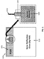
- FIG. 1 illustrates a passive RF structure 105 and an component 140 integrated onto a substrate in an embodiment 100.
- the passive RF structure 105 such as a Frequency Selective Surface (FSS)
- FSS Frequency Selective Surface
- the substrate 110 may be made of glass.
- a portion of the substrate 110 may also be coated with Ag NW for use as a solar reflective glass.
- An Ag NW film may be used as a transparent conductor for the component 140 or as an interconnect for passive circuit components.
- a graphene film may be used as transparent active channel material for making active RF devices, for example, a transistor.
- the component 140 may include a data out or intermediate frequency (IF) out port and a graphene low noise amplifier 130.
- IF intermediate frequency
- FIGs 2(a)-2(c) illustrate coplanar waveguide (CPW) fed slot antennas in various examples, whereby Figure 2(b) more closely corresponds to the invention.
- an antenna 200 is shown as an ideal reference antenna and includes a perfect electrical conductor (PEC) 225 and regions of glass 210 and 215.
- a PEC may be a conductor that does not produce losses and used to model antenna 200.
- Gold or copper may be in a realization of the antenna200.
- a realized gain may be approximately 2.7 dBi.
- the antenna 200 further includes an antenna feed point 205.
- the antenna may have a width of about 7.4mm and height of about 4.3mm.
- the antenna 200 may be configured with other heights and widths depending on the application.
- Figure 2(b) illustrates an antenna 240 similar to antenna 200 including a portion 255 formed from Ag NW in place of the PEC with a metal edge 250 formed along a slot.
- Figure 2(c) shows an antenna 251 similar to antenna 240 without the metal edge 250.
- Figure 2(d) illustrates a table 260 of electromagnetic simulation results in terms of antenna gain for the CPW fed slot antennas of Figures 2(a)-2(c) .
- Full electromagnetic simulation of the Ag NW antenna shows broadband performance at around 24 GHz with a maximum gain of better than 0dBi at 24 GHz.
- the antenna 240, 251 may be formed from copper or suitable conducting material.
- An Ag NW antenna may be formed as follows. Ag NW in a solution form may be applied or formed onto a host platform or surface. The Ag NW may be sprayed or spin coated on a glass substrate, such as a Pyrex® glass, or similar substrate. The Ag NW coated glass substrate may then be treated with acid to remove any oxidation layer and to enhance conductivity. A capping layer of aluminum oxide (Al 2 O 3 ), silicon dioxide (SiO 2 ), hafnium oxide (HfO 2 ), or any dielectric metal oxide may then be formed or applied to the Ag NW coated glass by atomic layer deposition (ALD), which is then followed by suitable lithography, etching and/or cleaning processes to pattern antennas, wires and interconnects. The capping layer may be applied to or formed on the Ag NW coated glass using spin coating, spray deposition, or chemical vapor deposition (CVD).
- ALD atomic layer deposition
- the Ag NW coated glass may be etched prior to coating with a dielectric material.
- the etchant may be an acid-based etchant, and may be used without dilution.
- An example of a suitable etchant may be found under the trade name Nickel etchant TFB available from the Transcnc Company, Inc., and may have chemical components including 15-20% nitric acid, less than one percent potassium perfluoroalkyl sulfonate, and water.
- a CPW fed slot type of Ag NW antenna may be designed and fabricated on glass for 24 GHz frequency band. Other suitable antenna designs may also be supported to achieve different frequency ranges.
- an antenna efficiency of about 50% or greater with transparent conductors having an optical transmittance of about 70% or more due to low conductivity (or equivalently a high sheet resistance) may be achieved.
- an Ag NW may be formed as the transparent conductor material for the antenna and graphene may be formed as a transparent active channel for the RF circuits due to electrical, thermal and/or mechanical properties.
- Ag NW film with the sheet resistance of less than 10 ohm/square at 85% optical transmission, and graphene having the sheet resistance of 50 ⁇ /sq at 50% optical transmittance may be used.
- efficiency of antennas or passive RF structures or interconnects made of Ag NW film may be increased by selectively enhancing the conductivity at edges of antenna radiator(s) or passive RF structures, including transmission lines or interconnects by embedding or adding thin strips, e.g. less than 10-12 microns, of higher conductivity metal where the currents are concentrated.
- the strips may be added or embedded near or around edge 250. This selective conductivity control approach may be also facilitated by selectively controlling the Ag NW layer density.
- the selective conductivity control method may improve a gain of the 50 ⁇ /sq transparent conductor antenna with 90% optical transmittance from -8.1dBi to -2.4dBi. It has also been determined that for a 120 micron long CPW line made from Ag NW having a sheet resistance of 5 ohm/sq, embedding 6 micrometer wide metal conductors along the edges of CPW line reduces a transmission loss from -0.88dB to - 0.025dB, as shown in Fig. 2(b) . An increase in antenna gain may also be obtained by integrating a transparent transistor amplifier with the antenna in the monolithic fabrication process, which may form an active antenna. Other RF functionality such as switching and mixing may be fabricated into the RF substrate in a similar manner.
- Figures 3(a)-3(c) illustrate cross-sectional views of optically transparent components in various embodiments.
- an optically transparent passive resistor 310, inductor 320, and/or capacitor 330 components may be formed.
- the passive components may use Ag NW for transparent interconnects.
- the resistor 310 may be formed on a glass substrate 315 with a layer of Ag NW 300 on a portion of the substrate 315.
- Graphene 305 may be used as a resistance material for the resistor and a desired resistance may be obtained by introducing controlled defects e.g. holes, slots, or similar structures, in the graphene, by controlling doping in graphene or controlling a number of graphene layers, controlling a width and/or length of the Graphene.
- Figure 3(b) shows an inductor 320 formed on a glass substrate 325 and a layer of Ag NW 323 on a portion of the substrate 325.
- the inductor 320 may be formed made from Ag NW using general spiral geometry. In one embodiment, the inductor may be formed by an etching process.
- Figure 3(c) shows a capacitor 330 which may be formed using silicon nitride (SiNx) or hafnium oxide (HfO 2 ) as a transparent dielectric material with Ag NW as ohmic contacts. Embedding of thin conductors to Ag NW may be applied when forming the passive components in order to increase effective conductivity of the Ag NW.
- Graphene may be grown on silicon (Si) and silicon carbide (SiC) wafer.
- the graphene film may be transferred onto a glass or transparent substrate or surface.
- the graphene film may be physically transferred onto a glass or transparent substrate by using a thermal release tape as a transfer medium.
- the graphene film may also be transferred using other known methods.
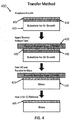
- Figure 4 illustrates a method of transferring graphene using a thermal release tape in an embodiment 400.
- the graphene layer 405 may be grown on a copper catalyst 410 on a substrate for graphene growth 415.
- a thermal release tape 420 may be applied to the graphene 405.
- the tape 420 may be peeled from the substrate in a conventional manner and applied to a substrate made from glass 430. Heat may be applied to the tape 420 at a suitable temperature to transfer the graphene to the glass substrate 430.
- One suitable temperature may be about 150°C.
- Figures 5(a)-5(b) illustrate an example of a fully transparent transistor that may be formed using graphene as an active channel layer and Ag NW as source and drain interconnect metal on top of a thin Ti/Au ohmic contact metal.
- Thin copper, Indium-tin Oxide (ITO) or Indium-zinc Oxide (IZO) may be used as optically transparent gate metal.
- the gate metal may have a thickness of tens of nanometers.
- Figures 5(a)-5(b) illustrate cross-sectional views of an optically transparent Field Effect Transistor (FET) in an embodiment.
- FET Field Effect Transistor
- FIG. 5(a) a cross-sectional view of the bottom-gate FET 510 having a source 504 and a drain 502, each formed from Ag NW and a layer of graphene 506 513 formed on a portion of an insulator 508.
- the FET 510 may also include a gate 513 and a substrate 515.
- Figure 5(b) shows a cross-sectional view of a top-gate FET 520 including a source 514 and a drain 512, each formed from Ag NW.
- the FET 520 further includes a gate 516 formed on at least a portion of an insulator 518.
- a layer of graphene 521 is configured between the insulator 518 and a substrate 525.
- Figure 6 illustrates a cross-sectional view of an optically transparent graphene active RF device 615 integrated with optically transparent passive RF structures in an embodiment 600.
- the active RF structure 615 may be monolithically fabricated on a transparent substrate or substantially transparent substrate 625.
- the graphene active device 615 may represent the device shown in Figures 5(a)-(b) .
- a graphene layer 610 may be optionally left on top of an Ag NW layer 605 to provide mechanical strength, thermal management, or a resistance to abrasion.
- the structure 600 may also include an Ag NW antenna 620, one or more slots 622, which may be configured as part of the CPW-fed slot antenna structure, and one or more thin metal lines 621.
- Active RF circuits generally require a thermal management capability.
- carbon-based graphene e.g., 4840-5300 W/mK may be used to provide thermal dissipation of active RF circuits on or in the glass substrate.
- an apparatus, system, and/or method are described to enable optically transparent reconfigurable integrated electrical components, such as antennas and RF circuits to be associated with an optically transparent host platform, such as glass.
- an Ag NW film may be configured as a transparent conductor for antennas and/or as interconnects for passive circuit components, such as capacitors or resistors. Ag NW may also be used as transmission lines and/or interconnect overlays for devices.
- a graphene film may also be configured as active channel material for making active RF devices, such as amplifiers and switches.
Landscapes
- Engineering & Computer Science (AREA)
- Microelectronics & Electronic Packaging (AREA)
- Manufacturing & Machinery (AREA)
- Chemical & Material Sciences (AREA)
- Power Engineering (AREA)
- Nanotechnology (AREA)
- Materials Engineering (AREA)
- Dispersion Chemistry (AREA)
- Astronomy & Astrophysics (AREA)
- Aviation & Aerospace Engineering (AREA)
- General Physics & Mathematics (AREA)
- Remote Sensing (AREA)
- Physics & Mathematics (AREA)
- Thin Film Transistor (AREA)
- Details Of Aerials (AREA)
Claims (13)
- Verfahren zur Bildung einer elektrischen Vorrichtung, wobei das Verfahren folgendes umfasst:Empfangen eines der folgenden: eines im Wesentlichen transparenten oder eines transparenten Substrats (525); undAusbilden eines Graphenfilms (521) auf einem Teil des Substrats (525);wobei das Verfahren dadurch gekennzeichnet ist, dass es ferner folgendes umfasst:Ausbilden einer Mehrzahl von Kontakten (512, 514) aus Silbernanodrähten auf einem Teil des Graphenfilms (521); wobei die Ränder der Kontakte eine erhöhte Leitfähigkeit aufweisen;wobei das Ausbilden einer Mehrzahl von Kontakten (502, 504; 512, 514) mit Rändern mit erhöhter Leitfähigkeit das Einbetten oder Hinzufügen dünner Streifen aus Metall mit hoher Leitfähigkeit an den Rändern der Kontakte umfasst; oder das selektive Erhöhen der Dichte von Silbernanodrähten an den Rändern der Kontakte.
- Verfahren zur Bildung einer elektrischen Vorrichtung, wobei das Verfahren folgendes umfasst:Empfangen eines der folgenden: eines im Wesentlichen transparenten oder eines transparenten Substrats (515);Ausbilden einer Gate-Elektrode (513) auf einem Teil des Substrats (515);Ausbilden eines Isolators (508) über der Gate-Elektrode (513); undAusbilden eines Graphenfilms (506) auf einem Teil des Isolators (508);wobei das Verfahren dadurch gekennzeichnet ist, dass es ferner folgendes umfasst:Ausbilden einer Mehrzahl von Kontakten (502, 504) aus Silbernanodrähten auf einem Teil des Graphenfilms (506); wobei die Ränder der Kontakte eine erhöhte Leitfähigkeit aufweisen;wobei das Ausbilden einer Mehrzahl von Kontakten (502, 504; 512, 514) mit Rändern mit erhöhter Leitfähigkeit das Einbetten oder Hinzufügen dünner Streifen aus Metall mit hoher Leitfähigkeit an den Rändern der Kontakte umfasst; oder das selektive Erhöhen der Dichte von Silbernanodrähten an den Rändern der Kontakte.
- Verfahren nach Anspruch 1 oder 2, wobei das Verfahren das Ausbilden der Mehrzahl von Kontakten (502, 504; 512, 514) auf einem dünnen Ti/Au ohmschen Kontaktmetall auf dem Teil des Graphenfilms (506; 521) umfasst.
- Verfahren nach Anspruch 1, wobei dieses ferner das Bereitstellen eines Gates (513; 516) umfasst, das aus einem der folgenden besteht: Gold, Kupfer, Indiumzinnoxid (ITO) und Indiumzinkoxid (IZO).
- Verfahren nach Anspruch 1, wobei dieses ferner das Bilden eines der folgenden umfasst: einer Antenne, einer frequenzselektiven Oberfläche, eines Widerstands, Kondensators und Induktors aus Silbernanodraht.
- Verfahren nach Anspruch 1, wobei dieses ferner folgendes umfasst:Bilden eines Isolators (518) über einem Teil des Graphenfilms (521); undBilden eines Gates (516) auf einem Teil des Isolators (518).
- Vorrichtung (510; 520), die folgendes umfasst:ein im Wesentlichen transparentes oder ein transparentes Substrat (515);eine Gate-Elektrode (513; 516); undeinen Graphenfilm (506; 521);wobei die Vorrichtung dadurch gekennzeichnet ist, dass sie ferner folgendes umfasst:eine Mehrzahl von Kontakten (502, 504; 512, 514), die aus Silbernanodrähten auf einem Teil des Graphenfilms (506; 521) ausgebildet sind, wobei die Ränder der Kontakte eine erhöhte Leitfähigkeit aufweisen,wobei das Ausbilden einer Mehrzahl von Kontakten (502, 504; 512, 514) mit Rändern mit erhöhter Leitfähigkeit das Einbetten oder Hinzufügen dünner Streifen aus Metall mit hoher Leitfähigkeit an den Rändern der Kontakte umfasst; oder das selektive Erhöhen der Dichte von Silbernanodrähten an den Rändern der Kontakte.
- Vorrichtung nach Anspruch 7, wobei die Ränder der Kontakte mit erhöhter Leitfähigkeit dünne Streifen aus einem Metall mit höherer Leitfähigkeit umfassen, die eingebettet oder hinzugefügt sind an den Rändern der Kontakte; oder Ränder mit selektiv erhöhter Dichte der Silbernanodrähte.
- Vorrichtung nach Anspruch 7,
wobei die Mehrzahl von Kontakten (502, 504; 512, 514) auf einem dünnen Ti/Au ohmschen Kontaktmetall ausgebildet ist, das auf dem Teil des Graphenfilms (506; 521) ausgebildet ist. - Vorrichtung nach Anspruch 7, wobei:die Gate-Elektrode (513) auf einem Teil des Substrats (515) ausgebildet ist; undein Isolator (508) über der Gate-Elektrode (513) ausgebildet ist;der Graphenfilm (506) auf einem Teil des Isolators (508) ausgebildet ist.
- Vorrichtung nach Anspruch 10,
wobei die Mehrzahl von Silbernanodrahtkontakten (502, 504) auf dem Graphenfilm (506) einen Source- und einen Drain-Anschluss eines Bottom-Gate-FET (510) bildet, mit der Gate-Elektrode (513) als Gate und dem Graphenfilm (506) als aktive Kanalschicht. - Vorrichtung nach Anspruch 7, wobei:der Graphenfilm (521) auf einem Teil des Substrats (525) ausgebildet ist;ein Isolator (518) über dem Graphenfilm (521) ausgebildet ist; unddie Gate-Elektrode (516) über einem Teil des Isolators (518) ausgebildet ist.
- Vorrichtung nach Anspruch 12,
wobei die Mehrzahl von Silbernanodrahtkontakten (512, 514) auf dem Graphenfilm (521) einen Source- und einen Drain-Anschluss eines Top-Gate-FET (520) bildet, mit der Gate-Elektrode (516) als Gate und dem Graphenfilm (521) als aktive Kanalschicht.
Applications Claiming Priority (2)
| Application Number | Priority Date | Filing Date | Title |
|---|---|---|---|
| US13/707,373 US8941095B2 (en) | 2012-12-06 | 2012-12-06 | Methods for integrating and forming optically transparent devices on surfaces |
| PCT/US2013/069317 WO2014088759A1 (en) | 2012-12-06 | 2013-11-08 | Forming transparent devices on surfaces |
Publications (3)
| Publication Number | Publication Date |
|---|---|
| EP2929545A1 EP2929545A1 (de) | 2015-10-14 |
| EP2929545A4 EP2929545A4 (de) | 2016-08-03 |
| EP2929545B1 true EP2929545B1 (de) | 2020-09-23 |
Family
ID=50879962
Family Applications (1)
| Application Number | Title | Priority Date | Filing Date |
|---|---|---|---|
| EP13860119.0A Active EP2929545B1 (de) | 2012-12-06 | 2013-11-08 | Herstellung durchsichtiger vorrichtungen auf oberflächen |
Country Status (4)
| Country | Link |
|---|---|
| US (2) | US8941095B2 (de) |
| EP (1) | EP2929545B1 (de) |
| CN (1) | CN104685578B (de) |
| WO (1) | WO2014088759A1 (de) |
Families Citing this family (35)
| Publication number | Priority date | Publication date | Assignee | Title |
|---|---|---|---|---|
| US9252252B2 (en) * | 2012-05-23 | 2016-02-02 | Ecole polytechnique fédérale de Lausanne (EPFL) | Ambipolar silicon nanowire field effect transistor |
| US10620431B2 (en) * | 2013-01-29 | 2020-04-14 | The Trustees Of Columbia University In The City Of New York | System, method and computer-accessible medium for depth of field imaging for three-dimensional sensing utilizing a spatial light modulator microscope arrangement |
| US9640680B1 (en) | 2013-02-19 | 2017-05-02 | Hrl Laboratories, Llc | Wide-band transparent electrical contacts and interconnects for FPAS and a method of making the same |
| US9548415B1 (en) | 2013-02-19 | 2017-01-17 | Hrl Laboratories, Llc | All-wavelength (VIS-LWIR) transparent electrical contacts and interconnects and methods of making them |
| CN104092013B (zh) * | 2014-07-18 | 2016-04-27 | 桂林电子科技大学 | 基于石墨烯的频率可重构天线 |
| US10825417B2 (en) | 2015-04-10 | 2020-11-03 | Ossia Inc. | Wirelessly powered electronic display apparatuses |
| KR20170141663A (ko) * | 2015-04-16 | 2017-12-26 | 바스프 에스이 | 패터닝된 투명 전도성 필름 및 이러한 패터닝된 투명 전도성 필름의 제조 방법 |
| CN105094231B (zh) * | 2015-07-28 | 2019-03-01 | 京东方科技集团股份有限公司 | 一种显示屏和便携设备 |
| US10446907B2 (en) * | 2016-02-16 | 2019-10-15 | GM Global Technology Operations LLC | Impedance surface treatment for mitigating surface waves and improving gain of antennas on glass |
| CN106229626A (zh) * | 2016-09-12 | 2016-12-14 | 深圳市金诺和信通讯有限公司 | 具有天线功能的透明面板、显示屏组件及无线通信设备 |
| CN111164828B (zh) | 2017-10-05 | 2021-12-03 | 伊斯曼柯达公司 | 透明天线 |
| US10847887B2 (en) | 2017-10-05 | 2020-11-24 | Eastman Kodak Company | Method for fabricating a transparent antenna |
| US10524356B2 (en) | 2017-10-05 | 2019-12-31 | Eastman Kodak Company | Transparent antenna |
| US10396061B1 (en) * | 2018-03-22 | 2019-08-27 | International Business Machines Corporation | Transparent electronics for invisible smart dust applications |
| CN108963448B (zh) * | 2018-06-26 | 2020-08-11 | 东南大学 | 一种光透明及频率可重构天线的加工方法 |
| WO2020061234A1 (en) * | 2018-09-19 | 2020-03-26 | Akash Systems, Inc. | Systems and methods for satellite communication |
| US11271303B2 (en) * | 2019-01-03 | 2022-03-08 | Boe Technology Group Co., Ltd. | Antenna, smart window, and method of fabricating antenna |
| CN112088464B (zh) * | 2019-03-18 | 2025-03-21 | Ask工业股份公司 | 带有集成加热器的天线的车辆后窗的制造方法 |
| CN110048224B (zh) | 2019-03-28 | 2021-05-11 | Oppo广东移动通信有限公司 | 天线模组和电子设备 |
| CN110021812B (zh) | 2019-04-08 | 2021-04-13 | Oppo广东移动通信有限公司 | 天线组件及电子设备 |
| CN110034388B (zh) * | 2019-04-18 | 2024-02-06 | 浙江清华柔性电子技术研究院 | 天线制备方法及具有其的天线 |
| CN112234362B (zh) | 2019-06-30 | 2022-03-01 | Oppo广东移动通信有限公司 | 壳体组件、天线组件及电子设备 |
| CN112235449B (zh) | 2019-06-30 | 2022-01-04 | Oppo广东移动通信有限公司 | 壳体组件、天线组件及电子设备 |
| EP3761450A1 (de) | 2019-06-30 | 2021-01-06 | Guangdong Oppo Mobile Telecommunications Corp., Ltd. | Gehäuseanordnung und elektronische vorrichtungen |
| CN110400775A (zh) * | 2019-07-10 | 2019-11-01 | 深圳市华星光电半导体显示技术有限公司 | 柔性阵列基板的制作方法及柔性阵列基板和柔性显示装置 |
| IT201900020838A1 (it) * | 2019-11-13 | 2021-05-13 | Wireless Network Sites Tech Srl | Corpo Illuminante con Antenne e Scambiatori di Calore Trasparenti |
| TWI719840B (zh) | 2019-11-15 | 2021-02-21 | 符仙瓊 | 應用於建築部件以增加射頻訊號穿透率之介電體結構及其設置方法 |
| CN112186363A (zh) * | 2020-09-24 | 2021-01-05 | 武汉汉烯科技有限公司 | 一种柔性宏观石墨烯频率选择表面 |
| US11563190B2 (en) * | 2020-12-09 | 2023-01-24 | Huawei Technologies Co., Ltd. | Graphene-based photodetector |
| CN115693111B (zh) * | 2021-07-26 | 2025-10-24 | 华为技术有限公司 | 一种电子设备 |
| JP7765040B2 (ja) * | 2021-12-21 | 2025-11-06 | 国立大学法人東北大学 | アンテナモジュールおよびその製造方法 |
| WO2024044047A1 (en) | 2022-08-25 | 2024-02-29 | Eastman Kodak Company | Heated planar antenna |
| US12311637B2 (en) | 2022-11-04 | 2025-05-27 | Agc Automotive Americas Co. | Laminated glazing assembly including an antenna assembly |
| JP2024176869A (ja) * | 2023-06-09 | 2024-12-19 | 国立大学法人東北大学 | 集積回路及びその製造方法 |
| WO2025253410A1 (en) * | 2024-06-07 | 2025-12-11 | Saint-Gobain Glass France | Automobile glazing |
Family Cites Families (19)
| Publication number | Priority date | Publication date | Assignee | Title |
|---|---|---|---|---|
| WO2006091823A2 (en) | 2005-02-25 | 2006-08-31 | The Regents Of The University Of California | Electronic devices with carbon nanotube components |
| CN101180765B (zh) | 2005-04-01 | 2013-06-05 | 日本写真印刷株式会社 | 显示器用透明天线和带天线的显示器用透光性构件以及带天线的壳体用构件 |
| US7289073B2 (en) | 2005-08-19 | 2007-10-30 | Gm Global Technology Operations, Inc. | Method for improving the efficiency of transparent thin film antennas and antennas made by such method |
| US7233296B2 (en) | 2005-08-19 | 2007-06-19 | Gm Global Technology Operations, Inc. | Transparent thin film antenna |
| GB0720268D0 (en) * | 2007-10-17 | 2007-11-28 | Pilkington Group Ltd | Glazing |
| US20110170330A1 (en) | 2008-09-23 | 2011-07-14 | National University Of Singapore | Graphene Memory Cell and Fabrication Methods Thereof |
| US8106838B2 (en) * | 2009-02-05 | 2012-01-31 | Research In Motion Limited | Mobile wireless communications device having diversity antenna system and related methods |
| US9012044B2 (en) * | 2009-08-03 | 2015-04-21 | 3M Innovative Properties Company | Process for forming optically clear conductive metal or metal alloy thin films and films made therefrom |
| KR101154347B1 (ko) | 2009-08-24 | 2012-06-13 | 한양대학교 산학협력단 | 그래핀 박막과 나노 입자를 이용한 광검출기 및 그 제조 방법 |
| JP2011066829A (ja) * | 2009-09-18 | 2011-03-31 | Panasonic Corp | 通信モジュール、通信装置 |
| EP2539904A4 (de) * | 2010-02-27 | 2018-01-10 | Innova Dynamics, Inc. | Strukturen mit in den oberflächen eingebetteten zusatzstoffen und herstellungsverfahren dafür |
| CN102823009B (zh) * | 2010-03-04 | 2015-09-16 | 佛罗里达大学研究基金会公司 | 包括电渗透源极层的半导体设备及其制造方法 |
| WO2011150321A1 (en) * | 2010-05-28 | 2011-12-01 | Massachusetts Institute Of Technology | Photon detector based on superconducting nanowires |
| US8952863B2 (en) | 2010-12-17 | 2015-02-10 | Nokia Corporation | Strain-tunable antenna and associated methods |
| WO2012112818A2 (en) * | 2011-02-16 | 2012-08-23 | The Regents Of The University Of California | Interpenetrating networks of crystalline carbon and nano-scale electroactive materials |
| US8692230B2 (en) | 2011-03-29 | 2014-04-08 | University Of Southern California | High performance field-effect transistors |
| WO2013003638A2 (en) * | 2011-06-28 | 2013-01-03 | Arjun Daniel Srinivas | Transparent conductors incorporating additives and related manufacturing methods |
| JP5583097B2 (ja) * | 2011-09-27 | 2014-09-03 | 株式会社東芝 | 透明電極積層体 |
| KR20120130149A (ko) * | 2012-10-26 | 2012-11-29 | 숭실대학교산학협력단 | 플렉시블 전계효과 트랜지스터 및 이의 제조 방법 |
-
2012
- 2012-12-06 US US13/707,373 patent/US8941095B2/en active Active
-
2013
- 2013-11-08 WO PCT/US2013/069317 patent/WO2014088759A1/en not_active Ceased
- 2013-11-08 CN CN201380051014.XA patent/CN104685578B/zh active Active
- 2013-11-08 EP EP13860119.0A patent/EP2929545B1/de active Active
-
2014
- 2014-12-04 US US14/560,888 patent/US9231213B2/en not_active Expired - Fee Related
Non-Patent Citations (1)
| Title |
|---|
| None * |
Also Published As
| Publication number | Publication date |
|---|---|
| US20140158987A1 (en) | 2014-06-12 |
| CN104685578A (zh) | 2015-06-03 |
| EP2929545A4 (de) | 2016-08-03 |
| CN104685578B (zh) | 2017-07-14 |
| EP2929545A1 (de) | 2015-10-14 |
| US9231213B2 (en) | 2016-01-05 |
| US20150084002A1 (en) | 2015-03-26 |
| US8941095B2 (en) | 2015-01-27 |
| WO2014088759A1 (en) | 2014-06-12 |
Similar Documents
| Publication | Publication Date | Title |
|---|---|---|
| EP2929545B1 (de) | Herstellung durchsichtiger vorrichtungen auf oberflächen | |
| Green et al. | Optically transparent antennas and filters: A smart city concept to alleviate infrastructure and network capacity challenges | |
| US8872725B1 (en) | Electronically-tunable flexible low profile microwave antenna | |
| US12068726B2 (en) | Monolithic microwave integrated circuit front-end module | |
| WO2006105510A1 (en) | Antenna-system using complement ary metal oxide semiconductor techniques | |
| Tong | Advanced materials and components for 5G and beyond | |
| Upadhyay et al. | A 60-GHz on-chip monopole antenna using silicon technology | |
| Karacolak et al. | Silicon carbide (SiC) antennas for high-temperature and high-power applications | |
| US9881883B2 (en) | Electronic device with microfilm antenna and related methods | |
| Borah et al. | A review on optically transparent antenna | |
| Vasu Babu et al. | Design and analysis of frequency selective surface for gain enhancement in terahertz applications | |
| US10056340B1 (en) | Flexible electronic circuit and method for manufacturing same | |
| Yang et al. | MEMS-loaded millimeter wave frequency reconfigurable quasi-Yagi dipole antenna | |
| Reddy et al. | A triple band flexible antenna using multi-layer graphene patch and polymer substrate | |
| Aliakbari et al. | On channel gain performance of car roof-glass embedded 5G antenna | |
| Ekke et al. | Gain enhancement of Microstrip patch Antenna Array by using substrate integrated waveguide for wireless communication system | |
| CN207705378U (zh) | 一种天线结构及电子设备 | |
| WO2025046878A1 (en) | Reconfigurable intelligent surface module and method of manufacturing thereof | |
| Geng et al. | Transparent power divider based on metal mesh and ITO composite structure | |
| Babu et al. | Design and Analysis of Frequency | |
| Jun et al. | A simple broadband stacked quasi-Yagi antenna | |
| Biglarbegian et al. | A 60 GHz on-chip slot antenna in silicon integrated passive device technology | |
| Emhemmed et al. | Integrated micromachined millimeter wave patch antenna | |
| Shafai et al. | Reduction of ohmic loss in planar circuits and antennas using laminated conductors | |
| CN120637825A (zh) | 一种基于氧化铪铁电电容的高性能毫米波传输线型移相器 |
Legal Events
| Date | Code | Title | Description |
|---|---|---|---|
| PUAI | Public reference made under article 153(3) epc to a published international application that has entered the european phase |
Free format text: ORIGINAL CODE: 0009012 |
|
| 17P | Request for examination filed |
Effective date: 20150629 |
|
| AK | Designated contracting states |
Kind code of ref document: A1 Designated state(s): AL AT BE BG CH CY CZ DE DK EE ES FI FR GB GR HR HU IE IS IT LI LT LU LV MC MK MT NL NO PL PT RO RS SE SI SK SM TR |
|
| AX | Request for extension of the european patent |
Extension state: BA ME |
|
| DAX | Request for extension of the european patent (deleted) | ||
| REG | Reference to a national code |
Ref country code: DE Ref legal event code: R079 Ref document number: 602013072829 Country of ref document: DE Free format text: PREVIOUS MAIN CLASS: H01B0005140000 Ipc: H01Q0001120000 |
|
| RA4 | Supplementary search report drawn up and despatched (corrected) |
Effective date: 20160630 |
|
| RIC1 | Information provided on ipc code assigned before grant |
Ipc: H05K 1/09 20060101ALI20160624BHEP Ipc: H01Q 1/28 20060101ALI20160624BHEP Ipc: H05K 1/18 20060101ALI20160624BHEP Ipc: H05K 1/02 20060101ALI20160624BHEP Ipc: H05K 3/06 20060101ALI20160624BHEP Ipc: H01Q 1/38 20060101ALI20160624BHEP Ipc: H01Q 1/32 20060101ALI20160624BHEP Ipc: H01Q 1/12 20060101AFI20160624BHEP Ipc: H01L 51/00 20060101ALI20160624BHEP Ipc: H01Q 13/10 20060101ALI20160624BHEP Ipc: H05K 3/46 20060101ALI20160624BHEP Ipc: H01Q 9/04 20060101ALI20160624BHEP Ipc: H01G 13/00 20130101ALI20160624BHEP |
|
| GRAP | Despatch of communication of intention to grant a patent |
Free format text: ORIGINAL CODE: EPIDOSNIGR1 |
|
| STAA | Information on the status of an ep patent application or granted ep patent |
Free format text: STATUS: GRANT OF PATENT IS INTENDED |
|
| INTG | Intention to grant announced |
Effective date: 20200415 |
|
| GRAS | Grant fee paid |
Free format text: ORIGINAL CODE: EPIDOSNIGR3 |
|
| GRAA | (expected) grant |
Free format text: ORIGINAL CODE: 0009210 |
|
| STAA | Information on the status of an ep patent application or granted ep patent |
Free format text: STATUS: THE PATENT HAS BEEN GRANTED |
|
| AK | Designated contracting states |
Kind code of ref document: B1 Designated state(s): AL AT BE BG CH CY CZ DE DK EE ES FI FR GB GR HR HU IE IS IT LI LT LU LV MC MK MT NL NO PL PT RO RS SE SI SK SM TR |
|
| REG | Reference to a national code |
Ref country code: GB Ref legal event code: FG4D |
|
| REG | Reference to a national code |
Ref country code: CH Ref legal event code: EP |
|
| REG | Reference to a national code |
Ref country code: IE Ref legal event code: FG4D |
|
| REG | Reference to a national code |
Ref country code: AT Ref legal event code: REF Ref document number: 1317313 Country of ref document: AT Kind code of ref document: T Effective date: 20201015 Ref country code: DE Ref legal event code: R096 Ref document number: 602013072829 Country of ref document: DE |
|
| PG25 | Lapsed in a contracting state [announced via postgrant information from national office to epo] |
Ref country code: BG Free format text: LAPSE BECAUSE OF FAILURE TO SUBMIT A TRANSLATION OF THE DESCRIPTION OR TO PAY THE FEE WITHIN THE PRESCRIBED TIME-LIMIT Effective date: 20201223 Ref country code: HR Free format text: LAPSE BECAUSE OF FAILURE TO SUBMIT A TRANSLATION OF THE DESCRIPTION OR TO PAY THE FEE WITHIN THE PRESCRIBED TIME-LIMIT Effective date: 20200923 Ref country code: SE Free format text: LAPSE BECAUSE OF FAILURE TO SUBMIT A TRANSLATION OF THE DESCRIPTION OR TO PAY THE FEE WITHIN THE PRESCRIBED TIME-LIMIT Effective date: 20200923 Ref country code: GR Free format text: LAPSE BECAUSE OF FAILURE TO SUBMIT A TRANSLATION OF THE DESCRIPTION OR TO PAY THE FEE WITHIN THE PRESCRIBED TIME-LIMIT Effective date: 20201224 Ref country code: NO Free format text: LAPSE BECAUSE OF FAILURE TO SUBMIT A TRANSLATION OF THE DESCRIPTION OR TO PAY THE FEE WITHIN THE PRESCRIBED TIME-LIMIT Effective date: 20201223 Ref country code: FI Free format text: LAPSE BECAUSE OF FAILURE TO SUBMIT A TRANSLATION OF THE DESCRIPTION OR TO PAY THE FEE WITHIN THE PRESCRIBED TIME-LIMIT Effective date: 20200923 |
|
| REG | Reference to a national code |
Ref country code: AT Ref legal event code: MK05 Ref document number: 1317313 Country of ref document: AT Kind code of ref document: T Effective date: 20200923 |
|
| PG25 | Lapsed in a contracting state [announced via postgrant information from national office to epo] |
Ref country code: RS Free format text: LAPSE BECAUSE OF FAILURE TO SUBMIT A TRANSLATION OF THE DESCRIPTION OR TO PAY THE FEE WITHIN THE PRESCRIBED TIME-LIMIT Effective date: 20200923 Ref country code: LV Free format text: LAPSE BECAUSE OF FAILURE TO SUBMIT A TRANSLATION OF THE DESCRIPTION OR TO PAY THE FEE WITHIN THE PRESCRIBED TIME-LIMIT Effective date: 20200923 |
|
| REG | Reference to a national code |
Ref country code: NL Ref legal event code: MP Effective date: 20200923 |
|
| REG | Reference to a national code |
Ref country code: LT Ref legal event code: MG4D |
|
| PG25 | Lapsed in a contracting state [announced via postgrant information from national office to epo] |
Ref country code: CZ Free format text: LAPSE BECAUSE OF FAILURE TO SUBMIT A TRANSLATION OF THE DESCRIPTION OR TO PAY THE FEE WITHIN THE PRESCRIBED TIME-LIMIT Effective date: 20200923 Ref country code: EE Free format text: LAPSE BECAUSE OF FAILURE TO SUBMIT A TRANSLATION OF THE DESCRIPTION OR TO PAY THE FEE WITHIN THE PRESCRIBED TIME-LIMIT Effective date: 20200923 Ref country code: SM Free format text: LAPSE BECAUSE OF FAILURE TO SUBMIT A TRANSLATION OF THE DESCRIPTION OR TO PAY THE FEE WITHIN THE PRESCRIBED TIME-LIMIT Effective date: 20200923 Ref country code: RO Free format text: LAPSE BECAUSE OF FAILURE TO SUBMIT A TRANSLATION OF THE DESCRIPTION OR TO PAY THE FEE WITHIN THE PRESCRIBED TIME-LIMIT Effective date: 20200923 Ref country code: NL Free format text: LAPSE BECAUSE OF FAILURE TO SUBMIT A TRANSLATION OF THE DESCRIPTION OR TO PAY THE FEE WITHIN THE PRESCRIBED TIME-LIMIT Effective date: 20200923 Ref country code: LT Free format text: LAPSE BECAUSE OF FAILURE TO SUBMIT A TRANSLATION OF THE DESCRIPTION OR TO PAY THE FEE WITHIN THE PRESCRIBED TIME-LIMIT Effective date: 20200923 Ref country code: PT Free format text: LAPSE BECAUSE OF FAILURE TO SUBMIT A TRANSLATION OF THE DESCRIPTION OR TO PAY THE FEE WITHIN THE PRESCRIBED TIME-LIMIT Effective date: 20210125 |
|
| PG25 | Lapsed in a contracting state [announced via postgrant information from national office to epo] |
Ref country code: ES Free format text: LAPSE BECAUSE OF FAILURE TO SUBMIT A TRANSLATION OF THE DESCRIPTION OR TO PAY THE FEE WITHIN THE PRESCRIBED TIME-LIMIT Effective date: 20200923 Ref country code: AT Free format text: LAPSE BECAUSE OF FAILURE TO SUBMIT A TRANSLATION OF THE DESCRIPTION OR TO PAY THE FEE WITHIN THE PRESCRIBED TIME-LIMIT Effective date: 20200923 Ref country code: AL Free format text: LAPSE BECAUSE OF FAILURE TO SUBMIT A TRANSLATION OF THE DESCRIPTION OR TO PAY THE FEE WITHIN THE PRESCRIBED TIME-LIMIT Effective date: 20200923 Ref country code: IS Free format text: LAPSE BECAUSE OF FAILURE TO SUBMIT A TRANSLATION OF THE DESCRIPTION OR TO PAY THE FEE WITHIN THE PRESCRIBED TIME-LIMIT Effective date: 20210123 Ref country code: PL Free format text: LAPSE BECAUSE OF FAILURE TO SUBMIT A TRANSLATION OF THE DESCRIPTION OR TO PAY THE FEE WITHIN THE PRESCRIBED TIME-LIMIT Effective date: 20200923 |
|
| REG | Reference to a national code |
Ref country code: DE Ref legal event code: R097 Ref document number: 602013072829 Country of ref document: DE |
|
| PG25 | Lapsed in a contracting state [announced via postgrant information from national office to epo] |
Ref country code: MC Free format text: LAPSE BECAUSE OF FAILURE TO SUBMIT A TRANSLATION OF THE DESCRIPTION OR TO PAY THE FEE WITHIN THE PRESCRIBED TIME-LIMIT Effective date: 20200923 Ref country code: SK Free format text: LAPSE BECAUSE OF FAILURE TO SUBMIT A TRANSLATION OF THE DESCRIPTION OR TO PAY THE FEE WITHIN THE PRESCRIBED TIME-LIMIT Effective date: 20200923 |
|
| REG | Reference to a national code |
Ref country code: CH Ref legal event code: PL |
|
| PG25 | Lapsed in a contracting state [announced via postgrant information from national office to epo] |
Ref country code: LU Free format text: LAPSE BECAUSE OF NON-PAYMENT OF DUE FEES Effective date: 20201108 |
|
| PLBE | No opposition filed within time limit |
Free format text: ORIGINAL CODE: 0009261 |
|
| STAA | Information on the status of an ep patent application or granted ep patent |
Free format text: STATUS: NO OPPOSITION FILED WITHIN TIME LIMIT |
|
| REG | Reference to a national code |
Ref country code: BE Ref legal event code: MM Effective date: 20201130 |
|
| GBPC | Gb: european patent ceased through non-payment of renewal fee |
Effective date: 20201223 |
|
| PG25 | Lapsed in a contracting state [announced via postgrant information from national office to epo] |
Ref country code: SI Free format text: LAPSE BECAUSE OF FAILURE TO SUBMIT A TRANSLATION OF THE DESCRIPTION OR TO PAY THE FEE WITHIN THE PRESCRIBED TIME-LIMIT Effective date: 20200923 Ref country code: LI Free format text: LAPSE BECAUSE OF NON-PAYMENT OF DUE FEES Effective date: 20201130 Ref country code: CH Free format text: LAPSE BECAUSE OF NON-PAYMENT OF DUE FEES Effective date: 20201130 Ref country code: DK Free format text: LAPSE BECAUSE OF FAILURE TO SUBMIT A TRANSLATION OF THE DESCRIPTION OR TO PAY THE FEE WITHIN THE PRESCRIBED TIME-LIMIT Effective date: 20200923 |
|
| 26N | No opposition filed |
Effective date: 20210624 |
|
| PG25 | Lapsed in a contracting state [announced via postgrant information from national office to epo] |
Ref country code: FR Free format text: LAPSE BECAUSE OF NON-PAYMENT OF DUE FEES Effective date: 20201123 Ref country code: IE Free format text: LAPSE BECAUSE OF NON-PAYMENT OF DUE FEES Effective date: 20201108 Ref country code: IT Free format text: LAPSE BECAUSE OF FAILURE TO SUBMIT A TRANSLATION OF THE DESCRIPTION OR TO PAY THE FEE WITHIN THE PRESCRIBED TIME-LIMIT Effective date: 20200923 |
|
| PG25 | Lapsed in a contracting state [announced via postgrant information from national office to epo] |
Ref country code: GB Free format text: LAPSE BECAUSE OF NON-PAYMENT OF DUE FEES Effective date: 20201223 |
|
| PG25 | Lapsed in a contracting state [announced via postgrant information from national office to epo] |
Ref country code: IS Free format text: LAPSE BECAUSE OF FAILURE TO SUBMIT A TRANSLATION OF THE DESCRIPTION OR TO PAY THE FEE WITHIN THE PRESCRIBED TIME-LIMIT Effective date: 20210123 Ref country code: TR Free format text: LAPSE BECAUSE OF FAILURE TO SUBMIT A TRANSLATION OF THE DESCRIPTION OR TO PAY THE FEE WITHIN THE PRESCRIBED TIME-LIMIT Effective date: 20200923 Ref country code: MT Free format text: LAPSE BECAUSE OF FAILURE TO SUBMIT A TRANSLATION OF THE DESCRIPTION OR TO PAY THE FEE WITHIN THE PRESCRIBED TIME-LIMIT Effective date: 20200923 Ref country code: CY Free format text: LAPSE BECAUSE OF FAILURE TO SUBMIT A TRANSLATION OF THE DESCRIPTION OR TO PAY THE FEE WITHIN THE PRESCRIBED TIME-LIMIT Effective date: 20200923 |
|
| PG25 | Lapsed in a contracting state [announced via postgrant information from national office to epo] |
Ref country code: MK Free format text: LAPSE BECAUSE OF FAILURE TO SUBMIT A TRANSLATION OF THE DESCRIPTION OR TO PAY THE FEE WITHIN THE PRESCRIBED TIME-LIMIT Effective date: 20200923 |
|
| PG25 | Lapsed in a contracting state [announced via postgrant information from national office to epo] |
Ref country code: BE Free format text: LAPSE BECAUSE OF NON-PAYMENT OF DUE FEES Effective date: 20201130 |
|
| P01 | Opt-out of the competence of the unified patent court (upc) registered |
Effective date: 20230523 |
|
| PGFP | Annual fee paid to national office [announced via postgrant information from national office to epo] |
Ref country code: DE Payment date: 20251128 Year of fee payment: 13 |