EP2929398B9 - Reflective optical element for euv lithography and method of manufacturing a reflective optical element - Google Patents
Reflective optical element for euv lithography and method of manufacturing a reflective optical element Download PDFInfo
- Publication number
- EP2929398B9 EP2929398B9 EP13811826.0A EP13811826A EP2929398B9 EP 2929398 B9 EP2929398 B9 EP 2929398B9 EP 13811826 A EP13811826 A EP 13811826A EP 2929398 B9 EP2929398 B9 EP 2929398B9
- Authority
- EP
- European Patent Office
- Prior art keywords
- thickness
- capping layer
- optical element
- reflective optical
- phase
- Prior art date
- Legal status (The legal status is an assumption and is not a legal conclusion. Google has not performed a legal analysis and makes no representation as to the accuracy of the status listed.)
- Active
Links
Images


Classifications
-
- G—PHYSICS
- G03—PHOTOGRAPHY; CINEMATOGRAPHY; ANALOGOUS TECHNIQUES USING WAVES OTHER THAN OPTICAL WAVES; ELECTROGRAPHY; HOLOGRAPHY
- G03F—PHOTOMECHANICAL PRODUCTION OF TEXTURED OR PATTERNED SURFACES, e.g. FOR PRINTING, FOR PROCESSING OF SEMICONDUCTOR DEVICES; MATERIALS THEREFOR; ORIGINALS THEREFOR; APPARATUS SPECIALLY ADAPTED THEREFOR
- G03F7/00—Photomechanical, e.g. photolithographic, production of textured or patterned surfaces, e.g. printing surfaces; Materials therefor, e.g. comprising photoresists; Apparatus specially adapted therefor
- G03F7/70—Microphotolithographic exposure; Apparatus therefor
- G03F7/70058—Mask illumination systems
- G03F7/702—Reflective illumination, i.e. reflective optical elements other than folding mirrors, e.g. extreme ultraviolet [EUV] illumination systems
-
- B—PERFORMING OPERATIONS; TRANSPORTING
- B82—NANOTECHNOLOGY
- B82Y—SPECIFIC USES OR APPLICATIONS OF NANOSTRUCTURES; MEASUREMENT OR ANALYSIS OF NANOSTRUCTURES; MANUFACTURE OR TREATMENT OF NANOSTRUCTURES
- B82Y10/00—Nanotechnology for information processing, storage or transmission, e.g. quantum computing or single electron logic
-
- G—PHYSICS
- G02—OPTICS
- G02B—OPTICAL ELEMENTS, SYSTEMS OR APPARATUS
- G02B17/00—Systems with reflecting surfaces, with or without refracting elements
- G02B17/02—Catoptric systems, e.g. image erecting and reversing system
- G02B17/06—Catoptric systems, e.g. image erecting and reversing system using mirrors only, i.e. having only one curved mirror
- G02B17/0647—Catoptric systems, e.g. image erecting and reversing system using mirrors only, i.e. having only one curved mirror using more than three curved mirrors
- G02B17/0663—Catoptric systems, e.g. image erecting and reversing system using mirrors only, i.e. having only one curved mirror using more than three curved mirrors off-axis or unobscured systems in which not all of the mirrors share a common axis of rotational symmetry, e.g. at least one of the mirrors is warped, tilted or decentered with respect to the other elements
-
- G—PHYSICS
- G02—OPTICS
- G02B—OPTICAL ELEMENTS, SYSTEMS OR APPARATUS
- G02B27/00—Optical systems or apparatus not provided for by any of the groups G02B1/00 - G02B26/00, G02B30/00
- G02B27/10—Beam splitting or combining systems
- G02B27/1006—Beam splitting or combining systems for splitting or combining different wavelengths
- G02B27/102—Beam splitting or combining systems for splitting or combining different wavelengths for generating a colour image from monochromatic image signal sources
- G02B27/1026—Beam splitting or combining systems for splitting or combining different wavelengths for generating a colour image from monochromatic image signal sources for use with reflective spatial light modulators
- G02B27/1033—Beam splitting or combining systems for splitting or combining different wavelengths for generating a colour image from monochromatic image signal sources for use with reflective spatial light modulators having a single light modulator for all colour channels
-
- G—PHYSICS
- G02—OPTICS
- G02B—OPTICAL ELEMENTS, SYSTEMS OR APPARATUS
- G02B5/00—Optical elements other than lenses
- G02B5/08—Mirrors
- G02B5/0816—Multilayer mirrors, i.e. having two or more reflecting layers
-
- G—PHYSICS
- G02—OPTICS
- G02B—OPTICAL ELEMENTS, SYSTEMS OR APPARATUS
- G02B5/00—Optical elements other than lenses
- G02B5/08—Mirrors
- G02B5/0891—Ultraviolet [UV] mirrors
-
- G—PHYSICS
- G03—PHOTOGRAPHY; CINEMATOGRAPHY; ANALOGOUS TECHNIQUES USING WAVES OTHER THAN OPTICAL WAVES; ELECTROGRAPHY; HOLOGRAPHY
- G03F—PHOTOMECHANICAL PRODUCTION OF TEXTURED OR PATTERNED SURFACES, e.g. FOR PRINTING, FOR PROCESSING OF SEMICONDUCTOR DEVICES; MATERIALS THEREFOR; ORIGINALS THEREFOR; APPARATUS SPECIALLY ADAPTED THEREFOR
- G03F7/00—Photomechanical, e.g. photolithographic, production of textured or patterned surfaces, e.g. printing surfaces; Materials therefor, e.g. comprising photoresists; Apparatus specially adapted therefor
- G03F7/70—Microphotolithographic exposure; Apparatus therefor
- G03F7/70216—Mask projection systems
- G03F7/70308—Optical correction elements, filters or phase plates for manipulating imaging light, e.g. intensity, wavelength, polarisation, phase or image shift
-
- G—PHYSICS
- G03—PHOTOGRAPHY; CINEMATOGRAPHY; ANALOGOUS TECHNIQUES USING WAVES OTHER THAN OPTICAL WAVES; ELECTROGRAPHY; HOLOGRAPHY
- G03F—PHOTOMECHANICAL PRODUCTION OF TEXTURED OR PATTERNED SURFACES, e.g. FOR PRINTING, FOR PROCESSING OF SEMICONDUCTOR DEVICES; MATERIALS THEREFOR; ORIGINALS THEREFOR; APPARATUS SPECIALLY ADAPTED THEREFOR
- G03F7/00—Photomechanical, e.g. photolithographic, production of textured or patterned surfaces, e.g. printing surfaces; Materials therefor, e.g. comprising photoresists; Apparatus specially adapted therefor
- G03F7/70—Microphotolithographic exposure; Apparatus therefor
- G03F7/70216—Mask projection systems
- G03F7/70316—Details of optical elements, e.g. of Bragg reflectors, extreme ultraviolet [EUV] multilayer or bilayer mirrors or diffractive optical elements
-
- G—PHYSICS
- G03—PHOTOGRAPHY; CINEMATOGRAPHY; ANALOGOUS TECHNIQUES USING WAVES OTHER THAN OPTICAL WAVES; ELECTROGRAPHY; HOLOGRAPHY
- G03F—PHOTOMECHANICAL PRODUCTION OF TEXTURED OR PATTERNED SURFACES, e.g. FOR PRINTING, FOR PROCESSING OF SEMICONDUCTOR DEVICES; MATERIALS THEREFOR; ORIGINALS THEREFOR; APPARATUS SPECIALLY ADAPTED THEREFOR
- G03F7/00—Photomechanical, e.g. photolithographic, production of textured or patterned surfaces, e.g. printing surfaces; Materials therefor, e.g. comprising photoresists; Apparatus specially adapted therefor
- G03F7/70—Microphotolithographic exposure; Apparatus therefor
- G03F7/708—Construction of apparatus, e.g. environment aspects, hygiene aspects or materials
- G03F7/70908—Hygiene, e.g. preventing apparatus pollution, mitigating effect of pollution or removing pollutants from apparatus
- G03F7/70916—Pollution mitigation, i.e. mitigating effect of contamination or debris, e.g. foil traps
-
- G—PHYSICS
- G03—PHOTOGRAPHY; CINEMATOGRAPHY; ANALOGOUS TECHNIQUES USING WAVES OTHER THAN OPTICAL WAVES; ELECTROGRAPHY; HOLOGRAPHY
- G03F—PHOTOMECHANICAL PRODUCTION OF TEXTURED OR PATTERNED SURFACES, e.g. FOR PRINTING, FOR PROCESSING OF SEMICONDUCTOR DEVICES; MATERIALS THEREFOR; ORIGINALS THEREFOR; APPARATUS SPECIALLY ADAPTED THEREFOR
- G03F7/00—Photomechanical, e.g. photolithographic, production of textured or patterned surfaces, e.g. printing surfaces; Materials therefor, e.g. comprising photoresists; Apparatus specially adapted therefor
- G03F7/70—Microphotolithographic exposure; Apparatus therefor
- G03F7/708—Construction of apparatus, e.g. environment aspects, hygiene aspects or materials
- G03F7/7095—Materials, e.g. materials for housing, stage or other support having particular properties, e.g. weight, strength, conductivity, thermal expansion coefficient
- G03F7/70958—Optical materials or coatings, e.g. with particular transmittance, reflectance or anti-reflection properties
-
- G—PHYSICS
- G21—NUCLEAR PHYSICS; NUCLEAR ENGINEERING
- G21K—TECHNIQUES FOR HANDLING PARTICLES OR IONISING RADIATION NOT OTHERWISE PROVIDED FOR; IRRADIATION DEVICES; GAMMA RAY OR X-RAY MICROSCOPES
- G21K1/00—Arrangements for handling particles or ionising radiation, e.g. focusing or moderating
- G21K1/06—Arrangements for handling particles or ionising radiation, e.g. focusing or moderating using diffraction, refraction or reflection, e.g. monochromators
- G21K1/062—Devices having a multilayer structure
Definitions
- the invention relates to a reflective optical element of an optical system for EUV lithography as well as to a method of manufacturing a reflective optical element of an optical system for EUV lithography.
- Microlithography is used for producing microstructured components, such as, for example, integrated circuits or LCDs.
- the microlithography process is carried out in a so-called projection exposure apparatus comprising an illumination device and a projection lens.
- a substrate e.g. a silicon wafer
- a light-sensitive layer photoresist
- EUV extreme ultraviolet
- the ultraviolet wavelength range for example with wavelengths between approximately 5 nm and 20 nm in particular, it is no longer possible to work in transmission with lens-like elements, but rather illumination lenses or projection lenses or else masks made of reflective optical elements with reflection coatings matched to the respective operating wavelength are designed on the basis of multilayer systems.
- EUV extreme ultraviolet
- Multilayer systems are alternately applied sub-layers of a material with a higher real part of the refractive index at the operating wavelength (also referred to as a spacer) and a material with a slower real part of the refractive index at the operating wavelength (also referred to as an absorber), with an absorber/spacer pair forming a stack with a specific period thickness, with the period thickness equaling the sum of the thicknesses of the individual sub-layers forming a stack.
- a crystal is simulated in a certain way, the lattice planes of which correspond to the absorber sub-layers at which Bragg reflection occurs.
- a stack can have one or more additional sub-layers in addition to the absorber sub-layer and the spacer sub-layer.
- these additional sub-layers can be employed to avoid chemical mixing between the absorber and spacer material, or else to create a stack which is particularly stable against thermal influences (for example when heating the mirror by light in the infrared wavelength range).
- EUV multillayer systems are disclosed in EP 1 291 680 A2 , EP 2 053 463 A1 and US 2010/195075 A1 .
- the optical systems of the projection exposure apparatuses must ensure a wavefront aberration which is as small as possible.
- a method of manufacturing a reflective optical element of an optical system for EUV lithography comprising a multilayer system for reflecting an incident electromagnetic wave having an operating wavelength in the EUV range, the reflected wave having a phase ⁇ , and a capping layer made from a capping layer material, wherein the method comprises the following steps:
- the phase ⁇ of the reflected electromagnetic wave can be influenced by the thickness d of a capping layer which is applied on the vacuum side to the multilayer system.
- the phase ⁇ of the reflected wave to a first approximation changes linearly with increasing capping layer thickness in some thickness regions, while the phase of the reflected wave to a first approximation remains substantially constant in other capping layer thickness regions.
- the thickness of the capping layer (which varies if a thickness profile is created in said capping layer) is selected in such a way that it is situated in a thickness region in which the phase ⁇ varies particularly strongly.
- the "linearity-region" in the dependency "phase of reflected wave vs. thickness of capping layer” (“ ⁇ vs. d-curve”) extends across an interval of values of the capping layer thickness d larger than 1 nm, particularly larger than 2nm, more particularly larger than 4nm. Furthermore, in embodiments of the disclosure, the "linearity-region” in the dependency "phase of reflected wave vs. thickness of capping layer” (“ ⁇ vs. d-curve”) extends across an interval of values of the phase of the reflected wave larger than 0.5nm, particular larger than 1nm.
- the difference between the maximum thickness and the minimum thickness in the thickness profile being created in the capping layer can e.g. be at least 0.2nm, particularly at least 0.5nm, more particularly at least 1 nm, and more particularly at least 1.5nm.
- the wording that in the "linearity-region” the phase of the reflected wave varies "substantially linearly” with the thickness of the capping layer is to be understood such that this linearity-region preferably also comprises regions in the dependency "phase of reflected wave vs. thickness of capping layer" (" ⁇ vs. d-curve") in which said dependency deviates from an exact linear dependency by not more than ⁇ 15%, particularly by not more than ⁇ 10%, more particularly by not more than ⁇ 5% (referred to the respective value according to the exact linear dependency/approximation).
- the proposed selection of the capping layer thicknesses renders it possible that already the local removal of the smallest amounts of capping layer can correct the wavefront aberration generated there. According to an aspect of the disclosure, during the mass production of such reflective optical elements this can render the undertaking of a correction possible, despite increasing manufacturing tolerances, such that all reflective optical elements have a substantially equal resultant phase ⁇ of the reflected electromagnetic wave at the operating wavelength.
- the thickness of the capping layer can be specifically modified as desired in order to at least partially compensate for a wavefront aberrations being present in the remaining optical systems, or - with other words - to achieve, by introducing a thickness variation or a wavefront correction, respectively, at the surface of a specific reflective optical element, a wavefront correction of the whole optical system.
- the present disclosure in particular comprises the concept to provide, in a reflective optical element having a targeted thickness modification or variation of its capping layer for the aim of at least partial compensation for wavefront aberrations being present in the remaining optical system, the capping layer in such a way that both the maximum thickness and the minimum thickness in the thickness profile being provided for said wavefront aberration compensation are between the "linearity borders" of the " ⁇ vs. d"-curve, i.e. in the region where the phase of the wave being reflected at the element varies substantially linearly with the thickness of the capping layer.
- the invention also takes into account the fact that a conventional wavefront correction approach using lenses, namely to first determine the wavefront aberration based on non-coated lens elements followed by a demounting of the non-coated lens elements, a figure correction and a layer deposition on these elements is not possible here, since non-coated mirror substrates do not exhibit a significant reflectivity for EUV-wavelengths.
- high reflecting (HR-)layers which are time-consuming in the manufacturing process, significantly contribute, due to their lateral variations in layer thickness, to the wavefront aberrations of EUV projection objectives.
- the capping layer can consist of a single sub-layer made of one material or else of a sub-layer system.
- the capping layer particularly preferably is a sub-layer made of ruthenium.
- Further suitable capping layer materials include e.g. rhodium or silicon nitride.
- ruthenium, rhodium or silicon nitride as capping layer leads not only to sufficiently extensive thickness regions of the capping layer, in which phase plateaus are formed, between which thickness regions with strongly decreasing phase ⁇ are formed. For the multilayer system lying therebelow, these materials were moreover found to be efficient protection against oxidation by hydrogen in the residual-gas atmosphere during the EUV lithography operation or against carbon-containing contamination.
- said step of creating a thickness profile in said capping layer is performed such that a wavefront aberration in said optical system is at least partially compensated by said reflective optical element.
- said step of creating a thickness profile in said capping layer is performed such that the variation in the phase ⁇ relative to the variation in the capping layer thickness d is greater than 25%, in particular greater than 35%, more particularly, greater than 40%. What this renders possible is that, even in the case of relatively large wavefront aberrations, a correction can already be carried out by removing small amounts of capping layer.
- said dependency is such that the phase ⁇ initially remains substantially constant in said dependency until a thickness d1 is reached, decreases between the thickness d1 and a further thickness d2, with d1 ⁇ d2, and remains substantially constant at a thickness greater than d2, wherein said step of creating a thickness profile in said capping layer is performed such that the resulting thicknesses d of the capping layer meet the condition d1 ⁇ d ⁇ d2.
- the invention also relates to a method of manufacturing a reflective optical element of an optical system for EUV lithography, said reflective optical element comprising a multilayer system for reflecting an incident electromagnetic wave having an operating wavelength in the EUV range, and a capping layer made from a capping layer material, wherein the method comprises the following steps:
- the disclosure also comprises the concept of adapting the layer thickness of the cap layer such that the reflectivity remains substantially constant over the whole region of thickness values that may be obtained in the ICA-correction process.
- a reduction of the absolute value of reflectivity across the mirror may be deliberately accepted.
- said step of creating a thickness profile in said capping layer is performed such that both the maximum thickness and the minimum thickness in the thickness profile are in the region from 1 nm to 4 nm.
- the capping layer material comprises ruthenium, rhodium or silicon nitride.
- the multilayer system has alternately arranged sub-layers made of silicon and molybdenum.
- the invention also relates to a reflective optical element for EUV lithography, characterized in that it is manufactured using a method as described above.
- the invention also relates to a reflective optical element for EUV lithography, comprising:
- said capping layer has a variation in the capping layer thickness such that the variation in the phase ⁇ relative to said variation in the capping layer thickness is greater than 35%, more particularly, greater than 40%.
- the invention also relates to an optical system for EUV lithography, comprising a reflective optical element as described above.
- the optical system is embodied as a projection system.
- Good imaging qualities by means of which the structures on a mask or a reticle are imaged on an object to be exposed, for example on a wafer, are important, particularly in projection systems in an EUV lithography device.
- a high imaging quality can be ensured.
- the parameter P(M) is also further discussed below.
- the reflective optical element is arranged close to a field plane of the optical system. It was found to be advantageous if the reflective optical element has a near-field arrangement in the optical system, particularly in a projection system. In the case of near-field optical elements, variations in the wavefront reflected thereon have a particularly strong effect.
- the capping layer thickness d particularly preferably lies in the range between approximately 1 nm and 10 nm, more particularly in the range from 1 nm to 4 nm. In this range, a region with strongly decreasing phase ⁇ can be formed between two phase plateaus, depending on the capping layer thickness. At the same time, the capping layer thickness is preferably sufficiently small so as not to have to accept excessively large drops in the reflectivity of the reflective optical element due to absorption in the capping layer.
- said dependency according to which the phase of the reflected wave varies with the thickness of the capping layer is such that the phase ⁇ initially remains substantially constant said dependency until a thickness d1 is reached, decreases between the thickness d1 and a further thickness d2, with d1 ⁇ d2, and remains substantially constant at a thickness greater than d2, wherein the thickness d of the capping layer (which varies if a thickness profile is created in the capping layer) is selected in such a way that it lies in the range between (d1+d2)/2 and d2.
- the thickness d can particularly lie between (d1+3*d2)/4 and d2.
- the multilayer system advantageously has alternately arranged sub-layers made of silicon and molybdenum.
- Multilayer systems based on silicon and molybdenum are particularly suitable for operating wavelengths in the range between 12.5 nm and 15 nm.
- the thickness of the sub-layer of the multilayer system adjoining the capping layer is selected in such a way that the reflectivity varies by less than 10%, particularly less than 5%, more particularly preferably less than 1%, over a region of values of the capping layer thickness d that is as large as possible, in particular over an interval of values of the capping layer thickness d larger than 1 nm, particularly larger than 2nm, more particularly larger than 4nm.
- the relative variation in the reflectivity compared to the maximum reflectivity that can be achieved in the relevant region. This selection of the sub-layer thickness reduces the risk of having to accept variations in the reflectivity which are too large when carrying out corrections of wavefront aberrations by virtue of removing capping layer.
- more than one sub-layer of the multilayer system can be varied in terms of the thickness thereof or this variation can be applied to the sub-layer lying below the sub-layer adjoining the capping layer or to an even deeper lying sub-layer in place of said sub-layer adjoining the capping layer.
- This likewise applies to the reflective optical elements referred to above.
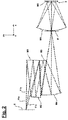
- Fig. 1 depicts, in an exemplary and very schematic manner, a lithographic projection exposure apparatus 1 with UV or EUV radiation.
- the projection exposure apparatus 1 has a light source 2. Illumination light 3 emerges from the light source, with the illumination light 3 being guided to an object field 5a in an object plane 5 using an illumination system 4 with optical elements not depicted here.
- a reticle 6 Arranged in the object plane 5 is a reticle 6 having a structure which, as image field, should be imaged on an object 9 arranged in the image plane 8.
- the object 9 to be exposed is a wafer which is held in the image plane 8 with the aid of an object holder 10.
- the object field in the object plane 5 is imaged on the wafer 9 in the image plane 8 using the projection system 7.
- a beam 3a emanating from the object plane 5 enters the projection system 7 and, as a beam 3b emerging from the projection system 7, impinges on the wafer 9 in the image plane with the desired linear magnification.
- the projection exposure apparatus 1 is a scanner-type apparatus. Both the reticle 6 and the object 9 are scanned in the y-direction during the operation of the projection exposure apparatus 1.
- Both one or else more mirrors of the illumination system 4 and, in particular, of the projection system 7 and also the reticle 6 can be a reflective optical element for an operating wavelength in the ultraviolet to extreme ultraviolet wavelength range.
- this can be a reflective optical element for EUV lithography, comprising a multilayer system for an operating wavelength in the extreme ultraviolet wavelength range, at which an incident electromagnetic wave at the operating wavelength can be reflected, the reflected wave having a phase ⁇ , and a capping layer with a thickness d, with the phase ⁇ varying depending on the thickness d, in which the phase variation relative to the capping layer thickness variation is greater than 25%, preferably greater than 40%.
- this can also be a reflective optical element for EUV lithography, comprising a multilayer system for an operating wavelength in the extreme ultraviolet wavelength range, at which an incident electromagnetic wave at the operating wavelength can be reflected, the reflected wave having a phase ⁇ , and a capping layer with a thickness d, with the phase ⁇ varying depending on the thickness d in such a way that the phase ⁇ initially remains substantially constant until a thickness d1 is reached, decreases between the thickness d1 and a further thickness d2, with d1 ⁇ d2, and remains substantially constant at a thickness greater than d2, in which the thickness d is selected in such a way that d1 ⁇ d ⁇ d2.
- Fig. 2 depicts, in an exemplary and schematic manner, an embodiment of the projection system 7 from Fig. 1 , which has six mirrors M1 to M6. Depending on the projection system, that can also be more or less than six mirrors. Depicted in Fig. 2 is the beam path of a central sub-beam 11 b and two sub-beams 11 a,c at the edge of an overall beam, which emanate from the object field in the object plane 5 and are imaged in the image field in the image plane 8 by means of the six mirrors M1 to M6.
- the mirrors M1 to M4 image the object plane 5 in an intermediate image plane 8'.
- the sub-beams 11 a-c cross at one point in the intermediate plane 8'.
- D(CR) 0 by definition.
- the value of the parameter P then equals 1. Accordingly, an optical element is arranged in the proximity of a pupil plane if P has a value close to 1.
- D(SA) 0 since the beam emanating from the field point of the object plane 5 collapses to a point at said location.
- the value of the parameter P then likewise is 0. Accordingly, an optical element is arranged in the proximity of a field plane if P has a value close to 0.
- a pupil plane of Fig. 2 Arranged centered in a pupil plane of Fig. 2 is an obscuration stop (not depicted). Using this, the sub-beams assigned to the central through-holes in the mirrors M5, M6 are obscured. The mirror M6, which together with the mirror M5 images the intermediate image field in the intermediate image plane 8' in the image plane 8, is arranged in the proximity of a further pupil plane.
- the embodiment of the projection system depicted in Fig. 2 is a system with central pupil obscuration.
- Each of the mirrors M1 to M6 can be one of the reflective optical elements described herein.
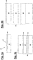
- Fig. 3a-c schematically depict the design of a reflective optical element 20.
- a substrate 22 Applied to a substrate 22 is a multilayer system 23, which substantially forms the reflective surface 21 (see Fig. 3a).
- Fig. 3b schematically shows the overarching structure of the multilayer system 23.
- the multilayer system 23 was produced by successive coating of a substrate 22 with different materials with different complex refractive indices.
- a capping layer 25 which can be made of several different material sub-layers, for protection against external influences such as e.g. contamination was additionally applied to the multilayer system 23.
- the thickness of the capping layer 25 can preferably be selected in such a way that, in the case of variations about this thickness, the variation in the phase ⁇ of the wave reflected at the reflective optical element 20 is as high as possible, in particular greater than 25%, preferably greater than 40%, relative to the variation in the thickness of the capping layer 25.
- the multilayer system 23 substantially consists of multiply repeating stacks 24, the structure of which is depicted schematically in Fig. 3c for a preferred embodiment and the thickness of which is also referred to as period thickness.
- the substantial sub-layers of a stack 24, which, in particular, by the multiple repetition of the stack 24, lead to sufficiently high reflection at an operating wavelength, are the so-called spacer sub-layers 26 made of a material with a higher real part of the refractive index and the so-called absorber sub-layers 27 made of a material with a lower real part of the refractive index.
- a crystal is simulated in a certain way, with the absorber sub-layers 27 corresponding to the lattice planes within the crystal, which have a distance from one another defined by the respective spacer sub-layers 26 and at which reflection of incident ultraviolet or, in particular, extreme ultraviolet radiation occurs.
- the thicknesses of the sub-layers are selected in such a way that, at a specific operating wavelength, the radiation reflected at each absorber sub-layer 27 interferes constructively in order thereby to achieve a high reflectivity of the reflective optical element. In so doing, the reflectivity obeys the Bragg condition and is therefore dependent not only on the wavelength but also on the angle of incidence.
- EUV lithography work is preferably done at e.g. wavelengths between 12 nm and 15 nm. In this wavelength range, it is possible to obtain particularly high reflectivities using multilayer systems on the basis of molybdenum as absorber material and silicon as spacer material. By way of example, at a wavelength of 13.5 nm, reflectivities in the region of up to 75% are theoretically possible. In so doing, use can be made, for example, of 50 to 60 stacks with a thickness of approximately 7 nm and a ratio of absorber sub-layer thickness to stack thickness of approximately 0.4.
- the thicknesses of the individual sub-layers 26, 27, 28 and also of the repeating stacks 24, i.e. the period thicknesses, can be constant over the entire multilayer system or else can vary, depending on what reflection profile is intended to be achieved.
- multilayer systems can be optimized for specific wavelengths, at which the maximum reflectivity and/or the reflected bandwidth is greater than at other wavelengths.
- the corresponding reflective optical element 20 is used, e.g. in EUV lithography, which is why this wavelength, for which the reflective optical element 20 was optimized, is also referred to as operating wavelength.
- multilayer systems can also be designed for other wavelengths up into the x-ray range or into the UV range.
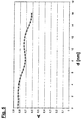
- Fig. 4a and 4b show the dependence of the phase ⁇ of a reflected electromagnetic wave on the capping layer thickness d.
- the reflective optical element is a standard multilayer system on the basis of alternately arranged sub-layers made of molybdenum as absorber and silicon as spacer, designed for an operating wavelength of 13.5 nm.
- the reflective optical element has a capping layer made of ruthenium with a thickness d.
- the behavior of the phase ⁇ of the electromagnetic wave, reflected at the optical element, with a wavelength of 13.5 nm compared to the incident electromagnetic wave was examined for various capping layer thicknesses of ruthenium between 0.5 nm and 21 nm.
- This phase difference is specified in units of nanometer (nm).
- Fig. 4a depicts the whole thickness range from 0.5 nm to 21 nm.
- Fig. 4b depicts, in slightly magnified fashion, the thickness range from 0.5 nm to 12 nm. Plateaus are formed in the thickness ranges 0.5 to 2.0 nm, 6.5 to 9.5 nm and 15.0 to 17.5 nm, in which the phase ⁇ is dependent only to a very small extent on the changing capping layer thickness d and can be considered to be substantially constant. In the remaining thickness ranges, the phase ⁇ to a first approximation changes linearly with the increasing capping layer thickness d. In particular, in the region between the plateaus, the variation in the phase ⁇ is greater than 25% of the change in the capping layer thickness.
- the phase difference in the thickness range from 2.0 nm to 6.5 nm changes from approximately 0.1 nm to approximately 1.5 nm, i.e. by more than 35%.
- the phase difference changes by approximately 1.4 nm, i.e. by more than 32%.
- the capping layer thickness d should be selected during the production thereof in such a way that it is situated between two plateau-like thickness regions.
- the capping layer thickness is preferably selected in such a way that it is closer to the upper edge of the respective thickness value range from d1 to d2 in order, where necessary, also to be able to correct relatively large wavefront aberrations.
- the thickness d of the capping layer is selected in such a way that it lies in the range between (d1+d2)/2 and d2; the thickness d is particularly preferably selected in such a way that it lies between (d1 +3*d2)/4 and d2.
- Fig. 5 shows the amplitude A of the reflected wave depending on the thickness of the capping layer for the reflective optical element from Fig. 4a,b and, in this case too, the fact that this is a superposition of individual partial waves and the fact that absorption takes place both within the multilayer system and in the capping layer were taken into account.
- the amplitude A drops from a value of more than 0.8 to slightly above 0.7.
- the reflectivity of the reflective optical element is calculated from the square of the amplitude A.
- the thickness range between 2 nm and 6 nm is preferred for the capping layer compared to the thickness between 10 nm and 15 nm. This is because significant drops in reflectivity are to be expected in the higher capping layer thickness range compared to the range between 2 nm and 6 nm.
- Fig. 6a,b depict the dependence of the reflectivity over a capping layer thickness range from 0 nm to 15 nm ( Fig. 6a ) and from 0 to 4 nm ( Fig. 6b ) for two different reflective optical elements.
- the dashed curve in Fig. 6a,b corresponds to the reflective optical element from Fig. 4a,b and 5 .
- the uppermost silicon sub-layer of the multilayer system was selected to be thinner by half in the reflective optical element corresponding to the solid curve in Fig. 6a ,b. As a result of this, the position of the reflectivity plateau shifts to higher capping layer thicknesses.
- the variation in the reflectivity in the range from 1 nm to 3 nm relative to the maximum reflectivity achievable in this range is less than 1.6%, i.e. significantly less than 10%, for the reflective optical element in accordance with the solid curve in Fig. 6a ,b.
- the thickness d of the capping layer is selected in such a way that it lies in the range between (d1+d2)/2 and d2; the thickness d is particularly preferably selected in such a way that it lies between (d1+3*d2)/4 and d2.
- the position and extent of the plateaus and the steep region in the phase difference profile can also be influenced in a targeted manner by the selection of the material or materials in the capping layer.
- Fig. 7a-c show schematic illustrations to explain a concept of creating a thickness profile in the capping layer in consideration of the standing wave field.
- Fig. 7a shows a standard capping layer 75 (which can e.g. be made of Ruthenium (Ru) and may have a thickness of e.g. 1.5nm to 2nm) deposited on a diffusion-barrier layer 78 as well as a multilayer system 73 of Mo-layers and Si-layers on a substrate 72.
- the layer stack is optimized in such a way that the standing wave field created by the multilayer system 73 has a maximum (denoted as "A" in Fig. 7a-c ) just at the (vacuum) interface to the capping layer 75.
- the thickness of the last silicon layer 74 in the multilayer system 73 is adapted in such a way a maximum in reflectivity is achieved.
- the capping layer 85 is initially enhanced in order to still provide, after the creation of a thickness profile as shown in Fig. 7c , the minimum required thickness of the capping layer 85.
- the capping layer 85 is initially enhanced in order to still provide, after the creation of a thickness profile as shown in Fig. 7c , the minimum required thickness of the capping layer 85.
- plateau-region in the dependency of the reflectivity vs in order to obtain the before-described plateau-region in the dependency of the reflectivity vs.
- the thicknesses of the last silicon layer 84 in the multilayer system 83 and of the capping layer 85 are selected such that, in average, the (vacuum) interface to the capping layer 85 is at the same position where it would be for the "standard cap” of Fig. 7a , i.e. such that the standing wave field created by the multilayer system 83 has a maximum (denoted as "A") just at this vacuum interface.
Landscapes
- Physics & Mathematics (AREA)
- General Physics & Mathematics (AREA)
- Engineering & Computer Science (AREA)
- Optics & Photonics (AREA)
- Health & Medical Sciences (AREA)
- Epidemiology (AREA)
- Public Health (AREA)
- Environmental & Geological Engineering (AREA)
- Life Sciences & Earth Sciences (AREA)
- Atmospheric Sciences (AREA)
- Chemical & Material Sciences (AREA)
- Nanotechnology (AREA)
- Spectroscopy & Molecular Physics (AREA)
- General Engineering & Computer Science (AREA)
- High Energy & Nuclear Physics (AREA)
- Crystallography & Structural Chemistry (AREA)
- Theoretical Computer Science (AREA)
- Mathematical Physics (AREA)
- Exposure And Positioning Against Photoresist Photosensitive Materials (AREA)
- Exposure Of Semiconductors, Excluding Electron Or Ion Beam Exposure (AREA)
- Optical Elements Other Than Lenses (AREA)
- Lenses (AREA)
Applications Claiming Priority (3)
| Application Number | Priority Date | Filing Date | Title |
|---|---|---|---|
| US201261734183P | 2012-12-06 | 2012-12-06 | |
| DE102012222466.1A DE102012222466A1 (de) | 2012-12-06 | 2012-12-06 | Reflektives optisches Element für die EUV-Lithographie |
| PCT/EP2013/075620 WO2014086905A1 (en) | 2012-12-06 | 2013-12-05 | Reflective optical element for euv lithography and method of manufacturing a reflective optical element |
Publications (3)
| Publication Number | Publication Date |
|---|---|
| EP2929398A1 EP2929398A1 (en) | 2015-10-14 |
| EP2929398B1 EP2929398B1 (en) | 2016-11-23 |
| EP2929398B9 true EP2929398B9 (en) | 2017-03-22 |
Family
ID=50778061
Family Applications (1)
| Application Number | Title | Priority Date | Filing Date |
|---|---|---|---|
| EP13811826.0A Active EP2929398B9 (en) | 2012-12-06 | 2013-12-05 | Reflective optical element for euv lithography and method of manufacturing a reflective optical element |
Country Status (6)
Families Citing this family (5)
| Publication number | Priority date | Publication date | Assignee | Title |
|---|---|---|---|---|
| DE102016212373A1 (de) * | 2016-07-07 | 2018-01-11 | Carl Zeiss Smt Gmbh | Optisches System, insbesondere für eine mikrolithographische Projektionsbelichtungsanlage |
| US10468149B2 (en) * | 2017-02-03 | 2019-11-05 | Globalfoundries Inc. | Extreme ultraviolet mirrors and masks with improved reflectivity |
| JP2021071543A (ja) | 2019-10-29 | 2021-05-06 | ギガフォトン株式会社 | 極端紫外光集光ミラー、極端紫外光生成装置、及び電子デバイスの製造方法 |
| DE102020203286A1 (de) * | 2020-03-13 | 2021-09-16 | 3D Global Holding Gmbh | Lentikularlinsen-Baugruppe zum Anbringen an einer Anzeigefläche |
| KR20240115334A (ko) * | 2022-04-01 | 2024-07-25 | 에이지씨 가부시키가이샤 | 반사형 마스크 블랭크, 반사형 마스크, 반사형 마스크 블랭크의 제조 방법 및 반사형 마스크의 제조 방법 |
Family Cites Families (16)
| Publication number | Priority date | Publication date | Assignee | Title |
|---|---|---|---|---|
| TWI267704B (en) * | 1999-07-02 | 2006-12-01 | Asml Netherlands Bv | Capping layer for EUV optical elements |
| EP1291680A2 (en) * | 2001-08-27 | 2003-03-12 | Nikon Corporation | Multilayer-film mirrors for use in extreme UV optical systems, and methods for manufacturing such mirrors exhibiting improved wave aberrations |
| DE10209493B4 (de) | 2002-03-07 | 2007-03-22 | Carl Zeiss Smt Ag | Verfahren zur Vermeidung von Kontamination auf optischen Elementen, Vorrichtung zur Regelung von Kontamination auf optischen Elementen und EUV-Lithographievorrichtung |
| DE10309084A1 (de) * | 2003-03-03 | 2004-09-16 | Carl Zeiss Smt Ag | Reflektives optisches Element und EUV-Lithographiegerät |
| JP4521753B2 (ja) * | 2003-03-19 | 2010-08-11 | Hoya株式会社 | 反射型マスクの製造方法及び半導体装置の製造方法 |
| EP1930771A1 (en) | 2006-12-04 | 2008-06-11 | Carl Zeiss SMT AG | Projection objectives having mirror elements with reflective coatings |
| JP5194547B2 (ja) * | 2007-04-26 | 2013-05-08 | 凸版印刷株式会社 | 極端紫外線露光用マスク及びマスクブランク |
| CN101836163B (zh) | 2007-08-20 | 2012-06-27 | 卡尔蔡司Smt有限责任公司 | 包括具有反射涂层的镜元件的投射物镜 |
| EP2053463B1 (en) * | 2007-10-23 | 2011-06-08 | Imec | Detection of contamination in EUV systems |
| JP5590044B2 (ja) * | 2009-12-09 | 2014-09-17 | 旭硝子株式会社 | Euvリソグラフィ用光学部材 |
| EP2511944A4 (en) * | 2009-12-09 | 2014-09-03 | Asahi Glass Co Ltd | A SUBSTRATE ESTABLISHED WITH A REFLECTIVE LAYER FOR EUV LITHOGRAPHY, REFLECTING MASK ROLLING FOR EUV LITHOGRAPHY, REFLECTIVE MASK FOR EUV LITHOGRAPHY, AND METHOD FOR PRODUCING THE SUBSTRATE EQUIPPED WITH A REFLECTIVE LAYER |
| DE102009054986B4 (de) * | 2009-12-18 | 2015-11-12 | Carl Zeiss Smt Gmbh | Reflektive Maske für die EUV-Lithographie |
| CN103229248B (zh) | 2010-09-27 | 2016-10-12 | 卡尔蔡司Smt有限责任公司 | 反射镜,包含这种反射镜的投射物镜,以及包含这种投射物镜的用于微光刻的投射曝光设备 |
| DE102010041502A1 (de) * | 2010-09-28 | 2012-03-29 | Carl Zeiss Smt Gmbh | Spiegel, Projektionsobjektiv mit einem solchen Spiegel und Projektionsbelichtungs-anlage für die Mikrolithographie mit einem solchen Projektionsobjektiv |
| DE102011076011A1 (de) * | 2011-05-18 | 2012-11-22 | Carl Zeiss Smt Gmbh | Reflektives optisches Element und optisches System für die EUV-Lithographie |
| DE102012222451A1 (de) | 2012-12-06 | 2014-06-26 | Carl Zeiss Smt Gmbh | Reflektives optisches Element für die EUV-Lithographie |
-
2012
- 2012-12-06 DE DE102012222466.1A patent/DE102012222466A1/de not_active Ceased
-
2013
- 2013-12-05 JP JP2015546004A patent/JP6309535B2/ja active Active
- 2013-12-05 KR KR1020157017603A patent/KR102127230B1/ko active Active
- 2013-12-05 EP EP13811826.0A patent/EP2929398B9/en active Active
- 2013-12-05 WO PCT/EP2013/075620 patent/WO2014086905A1/en active Application Filing
-
2015
- 2015-06-05 US US14/732,248 patent/US9606446B2/en not_active Expired - Fee Related
Also Published As
| Publication number | Publication date |
|---|---|
| JP6309535B2 (ja) | 2018-04-18 |
| EP2929398B1 (en) | 2016-11-23 |
| JP2016500449A (ja) | 2016-01-12 |
| US20150316851A1 (en) | 2015-11-05 |
| KR20150092240A (ko) | 2015-08-12 |
| DE102012222466A1 (de) | 2014-06-12 |
| US9606446B2 (en) | 2017-03-28 |
| WO2014086905A1 (en) | 2014-06-12 |
| EP2929398A1 (en) | 2015-10-14 |
| KR102127230B1 (ko) | 2020-07-07 |
Similar Documents
| Publication | Publication Date | Title |
|---|---|---|
| EP2583138B1 (en) | Mask for euv lithography, euv lithography system and method for optimising the imaging of a mask | |
| US7771898B2 (en) | Multilayer mirror, evaluation method, exposure apparatus, device manufacturing method | |
| EP2513721B1 (en) | Reflective mask for euv lithography | |
| US8937709B2 (en) | Reflective optical element for EUV lithography | |
| US9606446B2 (en) | Reflective optical element for EUV lithography and method of manufacturing a reflective optical element | |
| TWI440900B (zh) | 多層鏡及微影投影裝置 | |
| US8848167B2 (en) | Optical element for UV or EUV lithography with coatings having optimized stress and thickness | |
| WO2007043414A1 (ja) | 多層膜反射鏡、多層膜反射鏡の製造方法、光学系、露光装置及びデバイスの製造方法 | |
| US20040002009A1 (en) | Re-usable extreme ultraviolet lithography multilayer mask blank | |
| WO2007100144A1 (en) | Measurement apparatus, exposure apparatus having the same, and device manufacturing method | |
| EP1775604B1 (en) | Multilayer mirror manufacturing method, optical system manufacturing method, exposure apparatus, and device manufacturing method | |
| EP1536284A1 (en) | Phase shift mask and production method therefor and production method for semiconductor device | |
| TWI452440B (zh) | 多層鏡及微影裝置 | |
| WO2008080534A1 (en) | Catadioptric projection objective with tilted deflecting mirrors, projection exposure apparatus, projection exposure method, and mirror | |
| US20090075179A1 (en) | Extreme ultraviolet (euv) mask protection against inspection laser damage | |
| CN116745702A (zh) | 用于调节光学系统、特别是用于微光刻的光学系统的方法 | |
| JP2006194764A (ja) | 多層膜反射鏡および露光装置 | |
| WO2024027999A1 (en) | Reflective member for euv lithography | |
| JP2023546667A (ja) | Euvスペクトル範囲用の2値強度マスク | |
| JP2007059743A (ja) | 多層膜反射鏡および露光装置 |
Legal Events
| Date | Code | Title | Description |
|---|---|---|---|
| PUAI | Public reference made under article 153(3) epc to a published international application that has entered the european phase |
Free format text: ORIGINAL CODE: 0009012 |
|
| 17P | Request for examination filed |
Effective date: 20150611 |
|
| AK | Designated contracting states |
Kind code of ref document: A1 Designated state(s): AL AT BE BG CH CY CZ DE DK EE ES FI FR GB GR HR HU IE IS IT LI LT LU LV MC MK MT NL NO PL PT RO RS SE SI SK SM TR |
|
| AX | Request for extension of the european patent |
Extension state: BA ME |
|
| DAX | Request for extension of the european patent (deleted) | ||
| RIC1 | Information provided on ipc code assigned before grant |
Ipc: G03F 7/20 20060101AFI20160714BHEP Ipc: G21K 1/06 20060101ALI20160714BHEP Ipc: B82Y 10/00 20110101ALI20160714BHEP Ipc: G02B 5/08 20060101ALI20160714BHEP Ipc: G03F 1/22 20120101ALI20160714BHEP Ipc: G02B 17/06 20060101ALI20160714BHEP Ipc: G02B 27/10 20060101ALI20160714BHEP |
|
| GRAP | Despatch of communication of intention to grant a patent |
Free format text: ORIGINAL CODE: EPIDOSNIGR1 |
|
| INTG | Intention to grant announced |
Effective date: 20160822 |
|
| GRAS | Grant fee paid |
Free format text: ORIGINAL CODE: EPIDOSNIGR3 |
|
| GRAA | (expected) grant |
Free format text: ORIGINAL CODE: 0009210 |
|
| AK | Designated contracting states |
Kind code of ref document: B1 Designated state(s): AL AT BE BG CH CY CZ DE DK EE ES FI FR GB GR HR HU IE IS IT LI LT LU LV MC MK MT NL NO PL PT RO RS SE SI SK SM TR |
|
| REG | Reference to a national code |
Ref country code: GB Ref legal event code: FG4D |
|
| REG | Reference to a national code |
Ref country code: CH Ref legal event code: EP |
|
| REG | Reference to a national code |
Ref country code: IE Ref legal event code: FG4D |
|
| REG | Reference to a national code |
Ref country code: AT Ref legal event code: REF Ref document number: 848449 Country of ref document: AT Kind code of ref document: T Effective date: 20161215 |
|
| REG | Reference to a national code |
Ref country code: DE Ref legal event code: R096 Ref document number: 602013014539 Country of ref document: DE |
|
| REG | Reference to a national code |
Ref country code: NL Ref legal event code: FP |
|
| PG25 | Lapsed in a contracting state [announced via postgrant information from national office to epo] |
Ref country code: LV Free format text: LAPSE BECAUSE OF FAILURE TO SUBMIT A TRANSLATION OF THE DESCRIPTION OR TO PAY THE FEE WITHIN THE PRESCRIBED TIME-LIMIT Effective date: 20161123 |
|
| REG | Reference to a national code |
Ref country code: LT Ref legal event code: MG4D |
|
| REG | Reference to a national code |
Ref country code: AT Ref legal event code: MK05 Ref document number: 848449 Country of ref document: AT Kind code of ref document: T Effective date: 20161123 |
|
| PG25 | Lapsed in a contracting state [announced via postgrant information from national office to epo] |
Ref country code: NO Free format text: LAPSE BECAUSE OF FAILURE TO SUBMIT A TRANSLATION OF THE DESCRIPTION OR TO PAY THE FEE WITHIN THE PRESCRIBED TIME-LIMIT Effective date: 20170223 Ref country code: GR Free format text: LAPSE BECAUSE OF FAILURE TO SUBMIT A TRANSLATION OF THE DESCRIPTION OR TO PAY THE FEE WITHIN THE PRESCRIBED TIME-LIMIT Effective date: 20170224 Ref country code: LT Free format text: LAPSE BECAUSE OF FAILURE TO SUBMIT A TRANSLATION OF THE DESCRIPTION OR TO PAY THE FEE WITHIN THE PRESCRIBED TIME-LIMIT Effective date: 20161123 Ref country code: SE Free format text: LAPSE BECAUSE OF FAILURE TO SUBMIT A TRANSLATION OF THE DESCRIPTION OR TO PAY THE FEE WITHIN THE PRESCRIBED TIME-LIMIT Effective date: 20161123 |
|
| PG25 | Lapsed in a contracting state [announced via postgrant information from national office to epo] |
Ref country code: BE Free format text: LAPSE BECAUSE OF NON-PAYMENT OF DUE FEES Effective date: 20161231 Ref country code: PT Free format text: LAPSE BECAUSE OF FAILURE TO SUBMIT A TRANSLATION OF THE DESCRIPTION OR TO PAY THE FEE WITHIN THE PRESCRIBED TIME-LIMIT Effective date: 20170323 Ref country code: FI Free format text: LAPSE BECAUSE OF FAILURE TO SUBMIT A TRANSLATION OF THE DESCRIPTION OR TO PAY THE FEE WITHIN THE PRESCRIBED TIME-LIMIT Effective date: 20161123 Ref country code: AT Free format text: LAPSE BECAUSE OF FAILURE TO SUBMIT A TRANSLATION OF THE DESCRIPTION OR TO PAY THE FEE WITHIN THE PRESCRIBED TIME-LIMIT Effective date: 20161123 Ref country code: ES Free format text: LAPSE BECAUSE OF FAILURE TO SUBMIT A TRANSLATION OF THE DESCRIPTION OR TO PAY THE FEE WITHIN THE PRESCRIBED TIME-LIMIT Effective date: 20161123 Ref country code: PL Free format text: LAPSE BECAUSE OF FAILURE TO SUBMIT A TRANSLATION OF THE DESCRIPTION OR TO PAY THE FEE WITHIN THE PRESCRIBED TIME-LIMIT Effective date: 20161123 Ref country code: RS Free format text: LAPSE BECAUSE OF FAILURE TO SUBMIT A TRANSLATION OF THE DESCRIPTION OR TO PAY THE FEE WITHIN THE PRESCRIBED TIME-LIMIT Effective date: 20161123 Ref country code: HR Free format text: LAPSE BECAUSE OF FAILURE TO SUBMIT A TRANSLATION OF THE DESCRIPTION OR TO PAY THE FEE WITHIN THE PRESCRIBED TIME-LIMIT Effective date: 20161123 |
|
| PG25 | Lapsed in a contracting state [announced via postgrant information from national office to epo] |
Ref country code: DK Free format text: LAPSE BECAUSE OF FAILURE TO SUBMIT A TRANSLATION OF THE DESCRIPTION OR TO PAY THE FEE WITHIN THE PRESCRIBED TIME-LIMIT Effective date: 20161123 Ref country code: EE Free format text: LAPSE BECAUSE OF FAILURE TO SUBMIT A TRANSLATION OF THE DESCRIPTION OR TO PAY THE FEE WITHIN THE PRESCRIBED TIME-LIMIT Effective date: 20161123 Ref country code: RO Free format text: LAPSE BECAUSE OF FAILURE TO SUBMIT A TRANSLATION OF THE DESCRIPTION OR TO PAY THE FEE WITHIN THE PRESCRIBED TIME-LIMIT Effective date: 20161123 Ref country code: SK Free format text: LAPSE BECAUSE OF FAILURE TO SUBMIT A TRANSLATION OF THE DESCRIPTION OR TO PAY THE FEE WITHIN THE PRESCRIBED TIME-LIMIT Effective date: 20161123 Ref country code: CZ Free format text: LAPSE BECAUSE OF FAILURE TO SUBMIT A TRANSLATION OF THE DESCRIPTION OR TO PAY THE FEE WITHIN THE PRESCRIBED TIME-LIMIT Effective date: 20161123 |
|
| REG | Reference to a national code |
Ref country code: CH Ref legal event code: PL |
|
| REG | Reference to a national code |
Ref country code: DE Ref legal event code: R097 Ref document number: 602013014539 Country of ref document: DE |
|
| PG25 | Lapsed in a contracting state [announced via postgrant information from national office to epo] |
Ref country code: BG Free format text: LAPSE BECAUSE OF FAILURE TO SUBMIT A TRANSLATION OF THE DESCRIPTION OR TO PAY THE FEE WITHIN THE PRESCRIBED TIME-LIMIT Effective date: 20170223 Ref country code: SM Free format text: LAPSE BECAUSE OF FAILURE TO SUBMIT A TRANSLATION OF THE DESCRIPTION OR TO PAY THE FEE WITHIN THE PRESCRIBED TIME-LIMIT Effective date: 20161123 Ref country code: IT Free format text: LAPSE BECAUSE OF FAILURE TO SUBMIT A TRANSLATION OF THE DESCRIPTION OR TO PAY THE FEE WITHIN THE PRESCRIBED TIME-LIMIT Effective date: 20161123 Ref country code: BE Free format text: LAPSE BECAUSE OF FAILURE TO SUBMIT A TRANSLATION OF THE DESCRIPTION OR TO PAY THE FEE WITHIN THE PRESCRIBED TIME-LIMIT Effective date: 20161123 |
|
| PG25 | Lapsed in a contracting state [announced via postgrant information from national office to epo] |
Ref country code: MC Free format text: LAPSE BECAUSE OF FAILURE TO SUBMIT A TRANSLATION OF THE DESCRIPTION OR TO PAY THE FEE WITHIN THE PRESCRIBED TIME-LIMIT Effective date: 20161123 |
|
| PLBE | No opposition filed within time limit |
Free format text: ORIGINAL CODE: 0009261 |
|
| REG | Reference to a national code |
Ref country code: FR Ref legal event code: ST Effective date: 20170831 |
|
| STAA | Information on the status of an ep patent application or granted ep patent |
Free format text: STATUS: NO OPPOSITION FILED WITHIN TIME LIMIT |
|
| REG | Reference to a national code |
Ref country code: IE Ref legal event code: MM4A |
|
| PG25 | Lapsed in a contracting state [announced via postgrant information from national office to epo] |
Ref country code: LI Free format text: LAPSE BECAUSE OF NON-PAYMENT OF DUE FEES Effective date: 20161231 Ref country code: CH Free format text: LAPSE BECAUSE OF NON-PAYMENT OF DUE FEES Effective date: 20161231 Ref country code: FR Free format text: LAPSE BECAUSE OF NON-PAYMENT OF DUE FEES Effective date: 20170123 Ref country code: LU Free format text: LAPSE BECAUSE OF NON-PAYMENT OF DUE FEES Effective date: 20161205 |
|
| 26N | No opposition filed |
Effective date: 20170824 |
|
| PG25 | Lapsed in a contracting state [announced via postgrant information from national office to epo] |
Ref country code: SI Free format text: LAPSE BECAUSE OF FAILURE TO SUBMIT A TRANSLATION OF THE DESCRIPTION OR TO PAY THE FEE WITHIN THE PRESCRIBED TIME-LIMIT Effective date: 20161123 Ref country code: IE Free format text: LAPSE BECAUSE OF NON-PAYMENT OF DUE FEES Effective date: 20161205 |
|
| PG25 | Lapsed in a contracting state [announced via postgrant information from national office to epo] |
Ref country code: HU Free format text: LAPSE BECAUSE OF FAILURE TO SUBMIT A TRANSLATION OF THE DESCRIPTION OR TO PAY THE FEE WITHIN THE PRESCRIBED TIME-LIMIT; INVALID AB INITIO Effective date: 20131205 |
|
| PG25 | Lapsed in a contracting state [announced via postgrant information from national office to epo] |
Ref country code: MK Free format text: LAPSE BECAUSE OF FAILURE TO SUBMIT A TRANSLATION OF THE DESCRIPTION OR TO PAY THE FEE WITHIN THE PRESCRIBED TIME-LIMIT Effective date: 20161123 Ref country code: CY Free format text: LAPSE BECAUSE OF FAILURE TO SUBMIT A TRANSLATION OF THE DESCRIPTION OR TO PAY THE FEE WITHIN THE PRESCRIBED TIME-LIMIT Effective date: 20161123 Ref country code: IS Free format text: LAPSE BECAUSE OF FAILURE TO SUBMIT A TRANSLATION OF THE DESCRIPTION OR TO PAY THE FEE WITHIN THE PRESCRIBED TIME-LIMIT Effective date: 20161123 |
|
| GBPC | Gb: european patent ceased through non-payment of renewal fee |
Effective date: 20171205 |
|
| PG25 | Lapsed in a contracting state [announced via postgrant information from national office to epo] |
Ref country code: MT Free format text: LAPSE BECAUSE OF NON-PAYMENT OF DUE FEES Effective date: 20161205 |
|
| PG25 | Lapsed in a contracting state [announced via postgrant information from national office to epo] |
Ref country code: TR Free format text: LAPSE BECAUSE OF FAILURE TO SUBMIT A TRANSLATION OF THE DESCRIPTION OR TO PAY THE FEE WITHIN THE PRESCRIBED TIME-LIMIT Effective date: 20161123 |
|
| PG25 | Lapsed in a contracting state [announced via postgrant information from national office to epo] |
Ref country code: GB Free format text: LAPSE BECAUSE OF NON-PAYMENT OF DUE FEES Effective date: 20171205 |
|
| PG25 | Lapsed in a contracting state [announced via postgrant information from national office to epo] |
Ref country code: AL Free format text: LAPSE BECAUSE OF FAILURE TO SUBMIT A TRANSLATION OF THE DESCRIPTION OR TO PAY THE FEE WITHIN THE PRESCRIBED TIME-LIMIT Effective date: 20161123 |
|
| P01 | Opt-out of the competence of the unified patent court (upc) registered |
Effective date: 20230525 |
|
| PGFP | Annual fee paid to national office [announced via postgrant information from national office to epo] |
Ref country code: NL Payment date: 20231220 Year of fee payment: 11 Ref country code: DE Payment date: 20231214 Year of fee payment: 11 |
|
| REG | Reference to a national code |
Ref country code: DE Ref legal event code: R119 Ref document number: 602013014539 Country of ref document: DE |
|
| REG | Reference to a national code |
Ref country code: NL Ref legal event code: MM Effective date: 20250101 |