EP2928265B1 - Induktionsheizvorrichtung und induktionskochfeld - Google Patents
Induktionsheizvorrichtung und induktionskochfeld Download PDFInfo
- Publication number
- EP2928265B1 EP2928265B1 EP15161492.2A EP15161492A EP2928265B1 EP 2928265 B1 EP2928265 B1 EP 2928265B1 EP 15161492 A EP15161492 A EP 15161492A EP 2928265 B1 EP2928265 B1 EP 2928265B1
- Authority
- EP
- European Patent Office
- Prior art keywords
- pole
- supply
- heating device
- induction heating
- circuit
- Prior art date
- Legal status (The legal status is an assumption and is not a legal conclusion. Google has not performed a legal analysis and makes no representation as to the accuracy of the status listed.)
- Active
Links
- 230000006698 induction Effects 0.000 title claims description 76
- 238000010438 heat treatment Methods 0.000 title claims description 36
- 239000003990 capacitor Substances 0.000 claims description 16
- 239000002241 glass-ceramic Substances 0.000 claims description 3
- 230000003213 activating effect Effects 0.000 claims description 2
- 230000008901 benefit Effects 0.000 description 4
- 230000010355 oscillation Effects 0.000 description 4
- 238000010411 cooking Methods 0.000 description 2
- 230000005347 demagnetization Effects 0.000 description 2
- 230000003534 oscillatory effect Effects 0.000 description 2
- 230000004913 activation Effects 0.000 description 1
- 238000000576 coating method Methods 0.000 description 1
- 230000009849 deactivation Effects 0.000 description 1
- 230000005284 excitation Effects 0.000 description 1
- 230000006870 function Effects 0.000 description 1
- 230000004044 response Effects 0.000 description 1
Images

Classifications
-
- H—ELECTRICITY
- H05—ELECTRIC TECHNIQUES NOT OTHERWISE PROVIDED FOR
- H05B—ELECTRIC HEATING; ELECTRIC LIGHT SOURCES NOT OTHERWISE PROVIDED FOR; CIRCUIT ARRANGEMENTS FOR ELECTRIC LIGHT SOURCES, IN GENERAL
- H05B6/00—Heating by electric, magnetic or electromagnetic fields
- H05B6/02—Induction heating
- H05B6/06—Control, e.g. of temperature, of power
- H05B6/062—Control, e.g. of temperature, of power for cooking plates or the like
-
- H—ELECTRICITY
- H05—ELECTRIC TECHNIQUES NOT OTHERWISE PROVIDED FOR
- H05B—ELECTRIC HEATING; ELECTRIC LIGHT SOURCES NOT OTHERWISE PROVIDED FOR; CIRCUIT ARRANGEMENTS FOR ELECTRIC LIGHT SOURCES, IN GENERAL
- H05B2213/00—Aspects relating both to resistive heating and to induction heating, covered by H05B3/00 and H05B6/00
- H05B2213/03—Heating plates made out of a matrix of heating elements that can define heating areas adapted to cookware randomly placed on the heating plate
Definitions
- the invention relates to an induction heating device, in particular for an induction hob, with a number of resonant circuits, each resonant circuit having a first pole and a second pole and an induction coil for heating.
- the invention further relates to an induction hob with such induction heating device.
- Generic induction heaters are used to heat hotplates of an induction hob.
- a respective induction coil is then arranged below a hob plate of an induction hob and can electromagnetically transmit energy to a cookware, which is on the hob plate by swinging in a known manner.
- a generic induction heating device is in the document DE 10017176 A1 shown.
- a respective resonant circuit is operated by two respective supply transistors, which apply a pole of the resonant circuit to alternating potentials.
- the resonant circuit is thus excited to oscillate, and the induction coil can transmit energy in the manner described above.
- a high component demand arises on supply transistors, in particular when many resonant circuits are used. This is particularly the case when the induction heating is used for surface cooking, so can supply cookware at any point on a cooktop plate with energy.
- a high component requirement arises for driver stages for driving the supply transistors.
- the US 4,241,250 shows a similar induction heating device with a plurality of resonant circuits, wherein in each resonant circuit, an induction coil is provided for heating an induction hob.
- an AC voltage source is provided, and the entire induction heater has the structure of a bridge rectifier, as is known for induction heaters.
- the invention has for its object to provide an induction heater, which has a lower component requirements, especially in a high number of resonant circuits, as well as to provide an induction hob with such an improved induction heating.
- the invention relates to an induction heating device with a number of resonant circuits, each having a first pole and a second pole, each resonant circuit having an induction coil for heating or induction heating coil. Furthermore, it has a supply line, with which the respective first poles of the oscillating circuits are connected, as well as a first supply transistor and a second supply transistor, each having a first pole and a second pole.
- the first pole of the first supply transistor is connected to a source of an intermediate circuit voltage
- the second pole of the first supply transistor and the first pole of the second supply transistor are connected to the supply line.
- the second pole of the second supply transistor is connected to a reference terminal.
- each resonant circuit is associated with a switching transistor and wherein the first pole of the switching transistor is connected to the second pole of the resonant circuit and the second pole of the switching transistor is connected to the reference terminal
- each diodes or freewheeling diodes each having a first pole and a second pole, wherein each oscillating circuit is associated with a freewheeling diode.
- the first pole of the freewheeling diode is connected to the source and the second pole of the freewheeling diode is connected to the second pole of the respective resonant circuit.
- the induction heating device In the case of the induction heating device according to the invention, only one switching transistor is required per resonant circuit, whereas the two supply transistors act simultaneously for all oscillatory circuits. Already from a number of four resonant circuits thus results in a savings in the total number of transistors required. Especially with higher numbers of resonant circuits, the number of required transistors is reduced considerably. It should also be mentioned that cheaper driver components can be used for the supply transistors since, in contrast to the prior art, the respective resonant circuit instead of an active transistor has a passive freewheeling diode which does not require a driver stage.
- the supply line and other connections in the induction heating device can be realized, for example, by conductive coatings of a circuit board, by wires, lines or other current-carrying elements.
- the reference terminal is preferably a ground terminal, which can for example produce a ground, preferably a common ground.
- the supply transistors serve to provide an alternating voltage for all resonant circuits simultaneously. This not only saves the number of components, it also ensures that all resonant circuits are excited identically. This can be avoided unwanted noise.
- the supply transistors are typically designed with sufficient capacity to supply them accordingly when operating all oscillating circuits. For example, they can each have a power of a few kW.
- the switching transistors serve to switch the respective resonant circuit to which the switching transistor is connected on and off. When the respective switching transistor is turned on, the respective resonant circuit is in operation. If the respective switching transistor is switched non-conductive, the resonant circuit is not in operation. This allows a separate control of all resonant circuits of the induction heater.
- the switching transistors are preferably controlled by a respective switching driver circuit, which is designed to switch the respective switching transistor for activating the resonant circuit to turn on and switch to disable the resonant circuit non-conductive.
- a respective switching driver circuit which is designed to switch the respective switching transistor for activating the resonant circuit to turn on and switch to disable the resonant circuit non-conductive.
- a respective driver circuit is adapted to switch the switching transistor pulsed conductive, wherein a duty cycle is set in response to a desired power output of the resonant circuit.
- a pulsed drive as described can be used with a certain duty cycle, allowing virtually infinite adjustability.
- the driver circuits are preferably connected to a control device which is designed to generate an alternating voltage on the supply line by means of the supply transistors and / or to activate and deactivate oscillating circuits by means of the switching transistors and / or to adjust their power output.
- a control device can be embodied, for example, as a computer, as a microprocessor, as a microcontroller, as a programmable logic controller (PLC) or in another manner. It may comprise, for example, processor means and memory means, wherein instructions are stored in the memory means, in the execution of which the processor behaves in a defined manner.
- PLC programmable logic controller
- the control device enables overall control of the system and the execution of the functions already described above by means of only one device. It should be understood, however, that the controller may also be split, for example, into a part that controls the supply transistors and another part that controls the switching transistors.
- a respective resonant circuit has exactly one induction coil and one capacitor connected thereto. This corresponds to a simple embodiment of a resonant circuit.
- the induction coil and the capacitor are connected according to the invention in series. As a result, a series resonant circuit is formed.
- the induction coil is connected to the supply line and the capacitor is connected to the first pole of the resonant circuit associated switching transistor. This arrangement has proven to be advantageous.
- a diode or the aforementioned freewheeling diode is looped between the second pole of a respective resonant circuit and the source of the intermediate circuit voltage, whose anode is connected to the second pole of the resonant circuit.
- the first supply transistor and the second supply transistor together form a half-bridge. This corresponds to a proven design for generating an alternating potential.
- the source of the intermediate circuit voltage preferably has a pulsed voltage source and a DC link capacitor.
- a pulsed voltage source may, for example, comprise means for rectifying a mains voltage.
- the DC link capacitor ensures that the voltage is smoothed.
- the supply transistors and / or the switching transistors are formed as IGBT transistors. These have proven to be advantageous for the present application.
- the induction heating on at least four resonant circuits is mathematically an advantage in the number of required components to record.
- oscillating circuits for example at least ten oscillating circuits.
- the invention further relates to an induction hob with a hob plate, preferably made of glass ceramic, and arranged under the cooktop plate according to the invention induction heating device, as described above.
- the advantages for an induction hob described with reference to the hob plate according to the invention can be utilized. there can be used on all described with reference to the induction heater and variants variants. Illustrated benefits apply accordingly.
- the induction hob is designed as ceremoniesnindutationskochfeld.
- Suchêtnindutationskochfelder usually require a very large number of resonant circuits, which results in a particularly high saving of components by the embodiment of the invention just in this case.
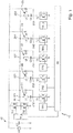
- the respective first poles 211, 221, 231, 241, 251 of the oscillating circuits 21, 22, 23, 24, 25 are all connected to a common supply line 30. This provides a common, alternating supply voltage for all resonant circuits 21, 22, 23, 24, 25 ready.
- the supply line 30 is connected to a first supply transistor TV1 and a second supply transistor TV2.
- the first supply transistor TV1 is connected at its pole 30 opposite the supply line to a source 40 of an intermediate circuit voltage which provides a rectified and smoothed voltage.
- the second supply transistor TV2 is connected to the supply line 30 opposite pole to the ground terminal.
- the two supply transistors TV1, TV2 are connected to a supply driver circuit TR_V, which alternately turns them on and off in an alternating manner. This means that always one of two supply transistors TV1, TV2 is conductive and the other is non-conductive. This generates a continuously changing potential at the supply line 30, which is suitable for the operation of the oscillating circuits 21, 22, 23, 24, 25, ie for their excitation.
- the supply transistors TV1, TV2 are driven with a frequency which corresponds to the resonant frequency of the oscillating circuits 21, 22, 23, 24, 25. This resonance frequency is advantageously identical in all oscillating circuits 21, 22, 23, 24, 25.
- the source 40 of the intermediate circuit voltage has a pulsed voltage source U1 and a DC link capacitor CZ.
- the pulsed voltage source U1 supplies a rectified, but not yet smoothed pulsating voltage.
- the DC link capacitor CZ smoothes this voltage, so that applied to the connected pole of the first supply transistor TV1 a smoothed voltage.
- diodes or freewheeling diodes D1, D2, D3, D4, Dn are also connected with their respective cathode to the source 40 of the intermediate circuit voltage.
- This voltage spikes which can occur in particular when switching off a respective switching transistor T1, T2, T3, T4, Tn due to the demagnetization of the coil can be derived and recycled in an advantageous manner. They are thus available again for operation of the induction heating device 10 and do not damage a component.
- the supply driver circuit TR_V and the switch driver circuits TR1, TR2, TR3, TR4, TR_n are connected to an electronic controller 50 which receives instructions for operating the induction heater 10 from a user in a manner not shown but known in the art. Accordingly, the supply driver circuit TR_V and the switch drive circuits TR1, TR2, TR3, TR4, TR_n are driven such that the transistors TV1, TV2, T1, T2, T3, T4, Tn are switched to provide the desired power output to the inductors L1, Generate L2, L3, L4, Ln. In particular, for this purpose, the switching driver circuits TR1, TR2, TR3, TR4, TR_n are driven such that they switch the switching transistors T1, T2, T3, T4, Tn pulsed conductive. The desired power output can be adjusted by the duty cycle.
- Fig. 2 shows an induction hob 100 with a hob plate 110 made of glass ceramic and an induction heater 10.
- the induction heater 10 is designed as that which in Fig. 1 is shown and described in connection with this figure. At individual components are in Fig. 2 however, only the inductors L1, L2, L3, L4, Ln are shown, while the other components are not explicitly shown.
- the induction coils L1, L2, L3, L4, Ln are arranged directly below the hob plate 110 and thus can be used for heating a set up on the hob plate 110 cookware.
- the induction hob 100 can be advantageously equipped with means not shown for detecting a pot position on the hob plate 110, so that only those induction coils L1, L2, L3, L4, Ln are operated, which is actually a pot or other cookware. This energy can be saved and the cooking comfort can be increased because a cookware can be placed anywhere.
Landscapes
- Physics & Mathematics (AREA)
- Electromagnetism (AREA)
- Induction Heating Cooking Devices (AREA)
- General Induction Heating (AREA)
Priority Applications (1)
| Application Number | Priority Date | Filing Date | Title |
|---|---|---|---|
| PL15161492T PL2928265T3 (pl) | 2014-04-03 | 2015-03-27 | Indukcyjne urządzenie grzewcze i indukcyjna płyta grzewcza |
Applications Claiming Priority (1)
| Application Number | Priority Date | Filing Date | Title |
|---|---|---|---|
| DE102014206458.9A DE102014206458A1 (de) | 2014-04-03 | 2014-04-03 | Induktionsheizvorrichtung und Induktionskochfeld |
Publications (2)
| Publication Number | Publication Date |
|---|---|
| EP2928265A1 EP2928265A1 (de) | 2015-10-07 |
| EP2928265B1 true EP2928265B1 (de) | 2019-01-09 |
Family
ID=52807643
Family Applications (1)
| Application Number | Title | Priority Date | Filing Date |
|---|---|---|---|
| EP15161492.2A Active EP2928265B1 (de) | 2014-04-03 | 2015-03-27 | Induktionsheizvorrichtung und induktionskochfeld |
Country Status (5)
| Country | Link |
|---|---|
| EP (1) | EP2928265B1 (es) |
| DE (1) | DE102014206458A1 (es) |
| ES (1) | ES2715448T3 (es) |
| PL (1) | PL2928265T3 (es) |
| TR (1) | TR201901346T4 (es) |
Families Citing this family (7)
| Publication number | Priority date | Publication date | Assignee | Title |
|---|---|---|---|---|
| ES2673131B1 (es) | 2016-12-19 | 2019-03-28 | Bsh Electrodomesticos Espana Sa | Dispositivo de aparato domestico de coccion por induccion con una matriz de elementos de calentamiento |
| DE102017211099A1 (de) * | 2017-06-29 | 2019-01-03 | E.G.O. Elektro-Gerätebau GmbH | Induktionskochvorrichtung und Verfahren zur Ansteuerung einer Induktionskochvorrichtung |
| KR102034798B1 (ko) | 2018-01-08 | 2019-10-21 | 엘지전자 주식회사 | 제어 알고리즘이 개선된 유도 가열 장치 |
| US20190327793A1 (en) * | 2018-04-23 | 2019-10-24 | Whirlpool Corporation | System and method for controlling induction heating devices with series connected switching devices |
| KR102626705B1 (ko) | 2018-10-10 | 2024-01-17 | 엘지전자 주식회사 | 스위치 스트레스 저감 구조가 개선된 유도 가열 장치 |
| EP4106491A1 (en) * | 2021-06-15 | 2022-12-21 | Aktiebolaget Electrolux | Induction cooking appliance |
| EP4106490A1 (en) * | 2021-06-15 | 2022-12-21 | Aktiebolaget Electrolux | Induction cooking appliance |
Family Cites Families (8)
| Publication number | Priority date | Publication date | Assignee | Title |
|---|---|---|---|---|
| US4241250A (en) * | 1979-06-25 | 1980-12-23 | General Electric Company | Induction cooking system |
| DE19654269C2 (de) * | 1995-12-27 | 2000-02-17 | Lg Electronics Inc | Induktionskochgerät |
| FR2792157B1 (fr) | 1999-04-09 | 2001-07-27 | Jaeger Regulation | Table de cuisson par induction comportant des foyers a induction alimentes par des generateurs |
| ES2353890B1 (es) * | 2008-12-19 | 2012-01-26 | Bsh Electrodomesticos España, S.A. | Campo de cocción con al menos tres zonas de calentamiento. |
| ES2355453B1 (es) * | 2008-12-19 | 2012-02-23 | Bsh Electrodomesticos España, S.A. | Campo de cocción con una pluralidad de elementos de calentamiento. |
| CN102282910B (zh) * | 2009-03-06 | 2013-08-28 | 三菱电机株式会社 | 感应加热烹调器 |
| FR2954661A1 (fr) * | 2009-12-23 | 2011-06-24 | Jaeger | Inducteurs sur phases equilibrees |
| TWI465218B (zh) * | 2011-09-05 | 2014-12-21 | Delta Electronics Inc | 具分時控制功能之電磁爐具架構及其操作方法 |
-
2014
- 2014-04-03 DE DE102014206458.9A patent/DE102014206458A1/de not_active Ceased
-
2015
- 2015-03-27 EP EP15161492.2A patent/EP2928265B1/de active Active
- 2015-03-27 TR TR2019/01346T patent/TR201901346T4/tr unknown
- 2015-03-27 ES ES15161492T patent/ES2715448T3/es active Active
- 2015-03-27 PL PL15161492T patent/PL2928265T3/pl unknown
Non-Patent Citations (1)
| Title |
|---|
| None * |
Also Published As
| Publication number | Publication date |
|---|---|
| PL2928265T3 (pl) | 2019-07-31 |
| DE102014206458A1 (de) | 2015-10-08 |
| ES2715448T3 (es) | 2019-06-04 |
| EP2928265A1 (de) | 2015-10-07 |
| TR201901346T4 (tr) | 2019-02-21 |
Similar Documents
| Publication | Publication Date | Title |
|---|---|---|
| EP2928265B1 (de) | Induktionsheizvorrichtung und induktionskochfeld | |
| EP1935213B1 (de) | Verfahren zum betrieb einer induktionsheizeinrichtung | |
| EP2380395B1 (de) | Kochfeld mit wenigstens drei heizzonen | |
| DE102004003126B4 (de) | Ansteuerungsverfahren für Heizelemente und Vorrichtung | |
| DE2535637A1 (de) | Induktionsheizvorrichtung | |
| WO2010069883A1 (de) | Induktionskochfeld und verfahren zum betreiben eines induktionskochfelds | |
| EP2095686A1 (de) | Heizvorrichtungsschaltung | |
| EP2469970B1 (de) | Gargerätevorrichtung | |
| EP2506663A1 (de) | Gargerätevorrichtung | |
| EP2520131B1 (de) | Gargerätevorrichtung | |
| EP2384083A1 (de) | Schaltungsanordnung für ein Induktionskochgerät, Verfahren zum Betreiben der Schaltungsanordnung und Induktionskochgerät | |
| EP2506665A2 (de) | Gargerätevorrichtung | |
| DE19708335A1 (de) | Heizleistungsregulierung für Induktionskochherd | |
| EP2506664B1 (de) | Gargerätevorrichtung | |
| DE102013207786A1 (de) | Hausgeräteinduktionsheizvorrichtung | |
| EP2548407B1 (de) | Kochmuldenvorrichtung | |
| EP3422815B1 (de) | Induktionskochvorrichtung und verfahren zur ansteuerung einer induktionskochvorrichtung | |
| EP2469971A1 (de) | Gargerätevorrichtung | |
| DE102005038525A1 (de) | Induktionskocheinrichtung mit einstellbarer Heizleistung | |
| EP2550841B1 (de) | Kochmuldenvorrichtung | |
| EP2506670B1 (de) | Induktionsheizvorrichtung | |
| DE102013221145B4 (de) | Induktionsheizeinrichtung | |
| DE112015001830T5 (de) | Induktions-Heizeinrichtung | |
| EP2876974B1 (de) | Gargerätevorrichtung | |
| EP4042834A1 (de) | Gargerätevorrichtung |
Legal Events
| Date | Code | Title | Description |
|---|---|---|---|
| PUAI | Public reference made under article 153(3) epc to a published international application that has entered the european phase |
Free format text: ORIGINAL CODE: 0009012 |
|
| AK | Designated contracting states |
Kind code of ref document: A1 Designated state(s): AL AT BE BG CH CY CZ DE DK EE ES FI FR GB GR HR HU IE IS IT LI LT LU LV MC MK MT NL NO PL PT RO RS SE SI SK SM TR |
|
| AX | Request for extension of the european patent |
Extension state: BA ME |
|
| 17P | Request for examination filed |
Effective date: 20160330 |
|
| RBV | Designated contracting states (corrected) |
Designated state(s): AL AT BE BG CH CY CZ DE DK EE ES FI FR GB GR HR HU IE IS IT LI LT LU LV MC MK MT NL NO PL PT RO RS SE SI SK SM TR |
|
| GRAP | Despatch of communication of intention to grant a patent |
Free format text: ORIGINAL CODE: EPIDOSNIGR1 |
|
| STAA | Information on the status of an ep patent application or granted ep patent |
Free format text: STATUS: GRANT OF PATENT IS INTENDED |
|
| INTG | Intention to grant announced |
Effective date: 20180724 |
|
| GRAS | Grant fee paid |
Free format text: ORIGINAL CODE: EPIDOSNIGR3 |
|
| GRAA | (expected) grant |
Free format text: ORIGINAL CODE: 0009210 |
|
| STAA | Information on the status of an ep patent application or granted ep patent |
Free format text: STATUS: THE PATENT HAS BEEN GRANTED |
|
| AK | Designated contracting states |
Kind code of ref document: B1 Designated state(s): AL AT BE BG CH CY CZ DE DK EE ES FI FR GB GR HR HU IE IS IT LI LT LU LV MC MK MT NL NO PL PT RO RS SE SI SK SM TR |
|
| REG | Reference to a national code |
Ref country code: GB Ref legal event code: FG4D Free format text: NOT ENGLISH |
|
| REG | Reference to a national code |
Ref country code: CH Ref legal event code: EP Ref country code: AT Ref legal event code: REF Ref document number: 1088948 Country of ref document: AT Kind code of ref document: T Effective date: 20190115 |
|
| REG | Reference to a national code |
Ref country code: IE Ref legal event code: FG4D Free format text: LANGUAGE OF EP DOCUMENT: GERMAN |
|
| REG | Reference to a national code |
Ref country code: DE Ref legal event code: R096 Ref document number: 502015007572 Country of ref document: DE |
|
| REG | Reference to a national code |
Ref country code: NL Ref legal event code: MP Effective date: 20190109 |
|
| REG | Reference to a national code |
Ref country code: LT Ref legal event code: MG4D |
|
| REG | Reference to a national code |
Ref country code: ES Ref legal event code: FG2A Ref document number: 2715448 Country of ref document: ES Kind code of ref document: T3 Effective date: 20190604 |
|
| PG25 | Lapsed in a contracting state [announced via postgrant information from national office to epo] |
Ref country code: NL Free format text: LAPSE BECAUSE OF FAILURE TO SUBMIT A TRANSLATION OF THE DESCRIPTION OR TO PAY THE FEE WITHIN THE PRESCRIBED TIME-LIMIT Effective date: 20190109 |
|
| PG25 | Lapsed in a contracting state [announced via postgrant information from national office to epo] |
Ref country code: FI Free format text: LAPSE BECAUSE OF FAILURE TO SUBMIT A TRANSLATION OF THE DESCRIPTION OR TO PAY THE FEE WITHIN THE PRESCRIBED TIME-LIMIT Effective date: 20190109 Ref country code: LT Free format text: LAPSE BECAUSE OF FAILURE TO SUBMIT A TRANSLATION OF THE DESCRIPTION OR TO PAY THE FEE WITHIN THE PRESCRIBED TIME-LIMIT Effective date: 20190109 Ref country code: SE Free format text: LAPSE BECAUSE OF FAILURE TO SUBMIT A TRANSLATION OF THE DESCRIPTION OR TO PAY THE FEE WITHIN THE PRESCRIBED TIME-LIMIT Effective date: 20190109 Ref country code: NO Free format text: LAPSE BECAUSE OF FAILURE TO SUBMIT A TRANSLATION OF THE DESCRIPTION OR TO PAY THE FEE WITHIN THE PRESCRIBED TIME-LIMIT Effective date: 20190409 Ref country code: PT Free format text: LAPSE BECAUSE OF FAILURE TO SUBMIT A TRANSLATION OF THE DESCRIPTION OR TO PAY THE FEE WITHIN THE PRESCRIBED TIME-LIMIT Effective date: 20190509 |
|
| PG25 | Lapsed in a contracting state [announced via postgrant information from national office to epo] |
Ref country code: GR Free format text: LAPSE BECAUSE OF FAILURE TO SUBMIT A TRANSLATION OF THE DESCRIPTION OR TO PAY THE FEE WITHIN THE PRESCRIBED TIME-LIMIT Effective date: 20190410 Ref country code: RS Free format text: LAPSE BECAUSE OF FAILURE TO SUBMIT A TRANSLATION OF THE DESCRIPTION OR TO PAY THE FEE WITHIN THE PRESCRIBED TIME-LIMIT Effective date: 20190109 Ref country code: BG Free format text: LAPSE BECAUSE OF FAILURE TO SUBMIT A TRANSLATION OF THE DESCRIPTION OR TO PAY THE FEE WITHIN THE PRESCRIBED TIME-LIMIT Effective date: 20190409 Ref country code: IS Free format text: LAPSE BECAUSE OF FAILURE TO SUBMIT A TRANSLATION OF THE DESCRIPTION OR TO PAY THE FEE WITHIN THE PRESCRIBED TIME-LIMIT Effective date: 20190509 Ref country code: HR Free format text: LAPSE BECAUSE OF FAILURE TO SUBMIT A TRANSLATION OF THE DESCRIPTION OR TO PAY THE FEE WITHIN THE PRESCRIBED TIME-LIMIT Effective date: 20190109 Ref country code: LV Free format text: LAPSE BECAUSE OF FAILURE TO SUBMIT A TRANSLATION OF THE DESCRIPTION OR TO PAY THE FEE WITHIN THE PRESCRIBED TIME-LIMIT Effective date: 20190109 |
|
| REG | Reference to a national code |
Ref country code: DE Ref legal event code: R097 Ref document number: 502015007572 Country of ref document: DE |
|
| PG25 | Lapsed in a contracting state [announced via postgrant information from national office to epo] |
Ref country code: AL Free format text: LAPSE BECAUSE OF FAILURE TO SUBMIT A TRANSLATION OF THE DESCRIPTION OR TO PAY THE FEE WITHIN THE PRESCRIBED TIME-LIMIT Effective date: 20190109 Ref country code: MC Free format text: LAPSE BECAUSE OF FAILURE TO SUBMIT A TRANSLATION OF THE DESCRIPTION OR TO PAY THE FEE WITHIN THE PRESCRIBED TIME-LIMIT Effective date: 20190109 Ref country code: EE Free format text: LAPSE BECAUSE OF FAILURE TO SUBMIT A TRANSLATION OF THE DESCRIPTION OR TO PAY THE FEE WITHIN THE PRESCRIBED TIME-LIMIT Effective date: 20190109 Ref country code: DK Free format text: LAPSE BECAUSE OF FAILURE TO SUBMIT A TRANSLATION OF THE DESCRIPTION OR TO PAY THE FEE WITHIN THE PRESCRIBED TIME-LIMIT Effective date: 20190109 Ref country code: RO Free format text: LAPSE BECAUSE OF FAILURE TO SUBMIT A TRANSLATION OF THE DESCRIPTION OR TO PAY THE FEE WITHIN THE PRESCRIBED TIME-LIMIT Effective date: 20190109 Ref country code: SK Free format text: LAPSE BECAUSE OF FAILURE TO SUBMIT A TRANSLATION OF THE DESCRIPTION OR TO PAY THE FEE WITHIN THE PRESCRIBED TIME-LIMIT Effective date: 20190109 Ref country code: CZ Free format text: LAPSE BECAUSE OF FAILURE TO SUBMIT A TRANSLATION OF THE DESCRIPTION OR TO PAY THE FEE WITHIN THE PRESCRIBED TIME-LIMIT Effective date: 20190109 |
|
| REG | Reference to a national code |
Ref country code: CH Ref legal event code: PL |
|
| PLBE | No opposition filed within time limit |
Free format text: ORIGINAL CODE: 0009261 |
|
| STAA | Information on the status of an ep patent application or granted ep patent |
Free format text: STATUS: NO OPPOSITION FILED WITHIN TIME LIMIT |
|
| PG25 | Lapsed in a contracting state [announced via postgrant information from national office to epo] |
Ref country code: SM Free format text: LAPSE BECAUSE OF FAILURE TO SUBMIT A TRANSLATION OF THE DESCRIPTION OR TO PAY THE FEE WITHIN THE PRESCRIBED TIME-LIMIT Effective date: 20190109 Ref country code: LU Free format text: LAPSE BECAUSE OF NON-PAYMENT OF DUE FEES Effective date: 20190327 |
|
| REG | Reference to a national code |
Ref country code: BE Ref legal event code: MM Effective date: 20190331 |
|
| 26N | No opposition filed |
Effective date: 20191010 |
|
| GBPC | Gb: european patent ceased through non-payment of renewal fee |
Effective date: 20190409 |
|
| PG25 | Lapsed in a contracting state [announced via postgrant information from national office to epo] |
Ref country code: GB Free format text: LAPSE BECAUSE OF NON-PAYMENT OF DUE FEES Effective date: 20190409 Ref country code: CH Free format text: LAPSE BECAUSE OF NON-PAYMENT OF DUE FEES Effective date: 20190331 Ref country code: LI Free format text: LAPSE BECAUSE OF NON-PAYMENT OF DUE FEES Effective date: 20190331 Ref country code: IE Free format text: LAPSE BECAUSE OF NON-PAYMENT OF DUE FEES Effective date: 20190327 |
|
| PG25 | Lapsed in a contracting state [announced via postgrant information from national office to epo] |
Ref country code: BE Free format text: LAPSE BECAUSE OF NON-PAYMENT OF DUE FEES Effective date: 20190331 Ref country code: SI Free format text: LAPSE BECAUSE OF FAILURE TO SUBMIT A TRANSLATION OF THE DESCRIPTION OR TO PAY THE FEE WITHIN THE PRESCRIBED TIME-LIMIT Effective date: 20190109 |
|
| PG25 | Lapsed in a contracting state [announced via postgrant information from national office to epo] |
Ref country code: MT Free format text: LAPSE BECAUSE OF FAILURE TO SUBMIT A TRANSLATION OF THE DESCRIPTION OR TO PAY THE FEE WITHIN THE PRESCRIBED TIME-LIMIT Effective date: 20190109 |
|
| REG | Reference to a national code |
Ref country code: AT Ref legal event code: MM01 Ref document number: 1088948 Country of ref document: AT Kind code of ref document: T Effective date: 20200327 |
|
| PG25 | Lapsed in a contracting state [announced via postgrant information from national office to epo] |
Ref country code: CY Free format text: LAPSE BECAUSE OF FAILURE TO SUBMIT A TRANSLATION OF THE DESCRIPTION OR TO PAY THE FEE WITHIN THE PRESCRIBED TIME-LIMIT Effective date: 20190109 |
|
| PG25 | Lapsed in a contracting state [announced via postgrant information from national office to epo] |
Ref country code: HU Free format text: LAPSE BECAUSE OF FAILURE TO SUBMIT A TRANSLATION OF THE DESCRIPTION OR TO PAY THE FEE WITHIN THE PRESCRIBED TIME-LIMIT; INVALID AB INITIO Effective date: 20150327 |
|
| PG25 | Lapsed in a contracting state [announced via postgrant information from national office to epo] |
Ref country code: AT Free format text: LAPSE BECAUSE OF NON-PAYMENT OF DUE FEES Effective date: 20200327 |
|
| PGFP | Annual fee paid to national office [announced via postgrant information from national office to epo] |
Ref country code: TR Payment date: 20220321 Year of fee payment: 8 Ref country code: PL Payment date: 20220317 Year of fee payment: 8 Ref country code: FR Payment date: 20220323 Year of fee payment: 8 |
|
| PG25 | Lapsed in a contracting state [announced via postgrant information from national office to epo] |
Ref country code: MK Free format text: LAPSE BECAUSE OF FAILURE TO SUBMIT A TRANSLATION OF THE DESCRIPTION OR TO PAY THE FEE WITHIN THE PRESCRIBED TIME-LIMIT Effective date: 20190109 |
|
| PGFP | Annual fee paid to national office [announced via postgrant information from national office to epo] |
Ref country code: IT Payment date: 20220331 Year of fee payment: 8 Ref country code: ES Payment date: 20220420 Year of fee payment: 8 |
|
| PG25 | Lapsed in a contracting state [announced via postgrant information from national office to epo] |
Ref country code: FR Free format text: LAPSE BECAUSE OF NON-PAYMENT OF DUE FEES Effective date: 20230331 |
|
| PG25 | Lapsed in a contracting state [announced via postgrant information from national office to epo] |
Ref country code: IT Free format text: LAPSE BECAUSE OF NON-PAYMENT OF DUE FEES Effective date: 20230327 |
|
| PGFP | Annual fee paid to national office [announced via postgrant information from national office to epo] |
Ref country code: DE Payment date: 20240321 Year of fee payment: 10 |
|
| REG | Reference to a national code |
Ref country code: ES Ref legal event code: FD2A Effective date: 20240528 |
|
| PG25 | Lapsed in a contracting state [announced via postgrant information from national office to epo] |
Ref country code: ES Free format text: LAPSE BECAUSE OF NON-PAYMENT OF DUE FEES Effective date: 20230328 |
|
| PG25 | Lapsed in a contracting state [announced via postgrant information from national office to epo] |
Ref country code: ES Free format text: LAPSE BECAUSE OF NON-PAYMENT OF DUE FEES Effective date: 20230328 |
|
| PG25 | Lapsed in a contracting state [announced via postgrant information from national office to epo] |
Ref country code: PL Free format text: LAPSE BECAUSE OF NON-PAYMENT OF DUE FEES Effective date: 20230327 |
|
| PG25 | Lapsed in a contracting state [announced via postgrant information from national office to epo] |
Ref country code: PL Free format text: LAPSE BECAUSE OF NON-PAYMENT OF DUE FEES Effective date: 20230327 |