EP2927982B1 - Organic light-emitting device including flexible substrate, and method for manufacturing same - Google Patents
Organic light-emitting device including flexible substrate, and method for manufacturing same Download PDFInfo
- Publication number
- EP2927982B1 EP2927982B1 EP13857827.3A EP13857827A EP2927982B1 EP 2927982 B1 EP2927982 B1 EP 2927982B1 EP 13857827 A EP13857827 A EP 13857827A EP 2927982 B1 EP2927982 B1 EP 2927982B1
- Authority
- EP
- European Patent Office
- Prior art keywords
- substrate
- emitting device
- organic light
- light emitting
- plastic substrate
- Prior art date
- Legal status (The legal status is an assumption and is not a legal conclusion. Google has not performed a legal analysis and makes no representation as to the accuracy of the status listed.)
- Active
Links
Images


Classifications
-
- H—ELECTRICITY
- H10—SEMICONDUCTOR DEVICES; ELECTRIC SOLID-STATE DEVICES NOT OTHERWISE PROVIDED FOR
- H10K—ORGANIC ELECTRIC SOLID-STATE DEVICES
- H10K71/00—Manufacture or treatment specially adapted for the organic devices covered by this subclass
-
- H—ELECTRICITY
- H10—SEMICONDUCTOR DEVICES; ELECTRIC SOLID-STATE DEVICES NOT OTHERWISE PROVIDED FOR
- H10K—ORGANIC ELECTRIC SOLID-STATE DEVICES
- H10K71/00—Manufacture or treatment specially adapted for the organic devices covered by this subclass
- H10K71/80—Manufacture or treatment specially adapted for the organic devices covered by this subclass using temporary substrates
-
- B—PERFORMING OPERATIONS; TRANSPORTING
- B32—LAYERED PRODUCTS
- B32B—LAYERED PRODUCTS, i.e. PRODUCTS BUILT-UP OF STRATA OF FLAT OR NON-FLAT, e.g. CELLULAR OR HONEYCOMB, FORM
- B32B17/00—Layered products essentially comprising sheet glass, or glass, slag, or like fibres
- B32B17/06—Layered products essentially comprising sheet glass, or glass, slag, or like fibres comprising glass as the main or only constituent of a layer, next to another layer of a specific material
- B32B17/10—Layered products essentially comprising sheet glass, or glass, slag, or like fibres comprising glass as the main or only constituent of a layer, next to another layer of a specific material of synthetic resin
-
- B—PERFORMING OPERATIONS; TRANSPORTING
- B32—LAYERED PRODUCTS
- B32B—LAYERED PRODUCTS, i.e. PRODUCTS BUILT-UP OF STRATA OF FLAT OR NON-FLAT, e.g. CELLULAR OR HONEYCOMB, FORM
- B32B27/00—Layered products comprising a layer of synthetic resin
- B32B27/28—Layered products comprising a layer of synthetic resin comprising synthetic resins not wholly covered by any one of the sub-groups B32B27/30 - B32B27/42
- B32B27/281—Layered products comprising a layer of synthetic resin comprising synthetic resins not wholly covered by any one of the sub-groups B32B27/30 - B32B27/42 comprising polyimides
-
- B—PERFORMING OPERATIONS; TRANSPORTING
- B32—LAYERED PRODUCTS
- B32B—LAYERED PRODUCTS, i.e. PRODUCTS BUILT-UP OF STRATA OF FLAT OR NON-FLAT, e.g. CELLULAR OR HONEYCOMB, FORM
- B32B7/00—Layered products characterised by the relation between layers; Layered products characterised by the relative orientation of features between layers, or by the relative values of a measurable parameter between layers, i.e. products comprising layers having different physical, chemical or physicochemical properties; Layered products characterised by the interconnection of layers
- B32B7/04—Interconnection of layers
- B32B7/06—Interconnection of layers permitting easy separation
-
- H—ELECTRICITY
- H10—SEMICONDUCTOR DEVICES; ELECTRIC SOLID-STATE DEVICES NOT OTHERWISE PROVIDED FOR
- H10K—ORGANIC ELECTRIC SOLID-STATE DEVICES
- H10K50/00—Organic light-emitting devices
- H10K50/80—Constructional details
- H10K50/84—Passivation; Containers; Encapsulations
-
- H—ELECTRICITY
- H10—SEMICONDUCTOR DEVICES; ELECTRIC SOLID-STATE DEVICES NOT OTHERWISE PROVIDED FOR
- H10K—ORGANIC ELECTRIC SOLID-STATE DEVICES
- H10K71/00—Manufacture or treatment specially adapted for the organic devices covered by this subclass
- H10K71/50—Forming devices by joining two substrates together, e.g. lamination techniques
-
- H—ELECTRICITY
- H10—SEMICONDUCTOR DEVICES; ELECTRIC SOLID-STATE DEVICES NOT OTHERWISE PROVIDED FOR
- H10K—ORGANIC ELECTRIC SOLID-STATE DEVICES
- H10K77/00—Constructional details of devices covered by this subclass and not covered by groups H10K10/80, H10K30/80, H10K50/80 or H10K59/80
- H10K77/10—Substrates, e.g. flexible substrates
- H10K77/111—Flexible substrates
-
- H—ELECTRICITY
- H10—SEMICONDUCTOR DEVICES; ELECTRIC SOLID-STATE DEVICES NOT OTHERWISE PROVIDED FOR
- H10K—ORGANIC ELECTRIC SOLID-STATE DEVICES
- H10K2102/00—Constructional details relating to the organic devices covered by this subclass
- H10K2102/301—Details of OLEDs
- H10K2102/311—Flexible OLED
-
- H—ELECTRICITY
- H10—SEMICONDUCTOR DEVICES; ELECTRIC SOLID-STATE DEVICES NOT OTHERWISE PROVIDED FOR
- H10K—ORGANIC ELECTRIC SOLID-STATE DEVICES
- H10K2102/00—Constructional details relating to the organic devices covered by this subclass
- H10K2102/301—Details of OLEDs
- H10K2102/351—Thickness
-
- H—ELECTRICITY
- H10—SEMICONDUCTOR DEVICES; ELECTRIC SOLID-STATE DEVICES NOT OTHERWISE PROVIDED FOR
- H10K—ORGANIC ELECTRIC SOLID-STATE DEVICES
- H10K50/00—Organic light-emitting devices
- H10K50/80—Constructional details
- H10K50/85—Arrangements for extracting light from the devices
-
- H—ELECTRICITY
- H10—SEMICONDUCTOR DEVICES; ELECTRIC SOLID-STATE DEVICES NOT OTHERWISE PROVIDED FOR
- H10K—ORGANIC ELECTRIC SOLID-STATE DEVICES
- H10K59/00—Integrated devices, or assemblies of multiple devices, comprising at least one organic light-emitting element covered by group H10K50/00
- H10K59/80—Constructional details
- H10K59/87—Passivation; Containers; Encapsulations
- H10K59/873—Encapsulations
-
- H—ELECTRICITY
- H10—SEMICONDUCTOR DEVICES; ELECTRIC SOLID-STATE DEVICES NOT OTHERWISE PROVIDED FOR
- H10K—ORGANIC ELECTRIC SOLID-STATE DEVICES
- H10K59/00—Integrated devices, or assemblies of multiple devices, comprising at least one organic light-emitting element covered by group H10K50/00
- H10K59/80—Constructional details
- H10K59/875—Arrangements for extracting light from the devices
-
- Y—GENERAL TAGGING OF NEW TECHNOLOGICAL DEVELOPMENTS; GENERAL TAGGING OF CROSS-SECTIONAL TECHNOLOGIES SPANNING OVER SEVERAL SECTIONS OF THE IPC; TECHNICAL SUBJECTS COVERED BY FORMER USPC CROSS-REFERENCE ART COLLECTIONS [XRACs] AND DIGESTS
- Y02—TECHNOLOGIES OR APPLICATIONS FOR MITIGATION OR ADAPTATION AGAINST CLIMATE CHANGE
- Y02E—REDUCTION OF GREENHOUSE GAS [GHG] EMISSIONS, RELATED TO ENERGY GENERATION, TRANSMISSION OR DISTRIBUTION
- Y02E10/00—Energy generation through renewable energy sources
- Y02E10/50—Photovoltaic [PV] energy
- Y02E10/549—Organic PV cells
-
- Y—GENERAL TAGGING OF NEW TECHNOLOGICAL DEVELOPMENTS; GENERAL TAGGING OF CROSS-SECTIONAL TECHNOLOGIES SPANNING OVER SEVERAL SECTIONS OF THE IPC; TECHNICAL SUBJECTS COVERED BY FORMER USPC CROSS-REFERENCE ART COLLECTIONS [XRACs] AND DIGESTS
- Y02—TECHNOLOGIES OR APPLICATIONS FOR MITIGATION OR ADAPTATION AGAINST CLIMATE CHANGE
- Y02P—CLIMATE CHANGE MITIGATION TECHNOLOGIES IN THE PRODUCTION OR PROCESSING OF GOODS
- Y02P70/00—Climate change mitigation technologies in the production process for final industrial or consumer products
- Y02P70/50—Manufacturing or production processes characterised by the final manufactured product
Definitions
- the present application relates to an organic light emitting device including a flexible substrate and a preparing method thereof.
- An organic light emitting device is formed by two opposing electrodes and organic material thin films having a plurality of layers having semiconductor-like properties interposed therebetween.
- the organic light emitting device having the aforementioned configuration uses a phenomenon in which electric energy is converted into light energy by using an organic material, that is, an organic light emitting phenomenon. Specifically, when voltage is applied between two electrodes in a structure in which an organic material layer is disposed between an anode and a cathode, holes from the anode and electrons from the cathode are injected into the organic material layer. When the injected holes and electrons meet each other, an exciton is formed, and the exciton falls down to a bottom state again to emit light.
- the organic light emitting device In the aforementioned organic light emitting device, light generated from the organic material layer is emitted through a light-transmitting electrode, and the organic light emitting device may be typically classified into a top emission type, a bottom-emission type, and a dual emission type. In the case of the top emission or bottom emission type, one of two electrodes needs to be a light transmitting electrode, and in the case of the dual emission type, all the two electrodes need to be light transmitting electrodes.
- the element In order to use the organic light emitting device as lighting, the element needs to be driven at high brightness unlike the existing natural color display, and constant brightness needs to be maintained like the existing lighting.
- constant brightness In order to sufficiently improve the brightness of the organic light emitting device, light emission needs to be implemented in a large area, and in order to implement light emission in the large area, a high driving current needs to be used.
- the aforementioned high current needs to be uniformly injected into the device having the large area.
- KR 2012 0100274 A describes a manufacturing method comprising a step of providing the carrier substrate, a step of forming a sacrificial layer on a fullerene (fullerene group) on an upper carrier substrate or a polyimide resin including the fluoro group, a step of forming a flexible substrate on a sacrificial layer, a step of forming a display device on the flexible substrate and a step of separating the flexible substrate which includes from the sacrificial layer the display device.
- US 2008/0053604 A1 describes a method including the steps of preparing a carrier substrate; stacking an adhesive layer on the carrier substrate, and stacking a flexible substrate having at least one image display device on the adhesive layer using a laminating or pressing method.
- the flexible substrate is easily fabricated without modification of conventional mass production equipment for fabricating a display, and thereby a lightweight, thin, and compact flexible display can be realized.
- US 2011/0003442 A1 describes a method for making a flexible semiconductor device including the following steps: A rigid substrate is provided. A flexible substrate is provided, and placed on the rigid substrate. A semiconductor device is directly fromed on the flexible substrate using a semiconductor process. After the rigid substrate is removed, the flexible semiconductor device is formed.
- US 2012/0171454 A1 relates to a glass/resin laminate containing for example an organic EL element on a glass substrate and a resin layer, in which the resin layer contains a polyimide obtained by condensation-polymerization of an aromatic diamine having a benzoxazole structure with an aromatic tetracarboxylic anhydride, the difference in the average linear expansion coefficient at 25 to 300° C between the glass substrate and the resin layer is from -100 ⁇ 10 7 to +100 ⁇ 10 7 /°C, and at least one outermost layer of the laminate is the glass substrate.
- the resin layer contains a polyimide obtained by condensation-polymerization of an aromatic diamine having a benzoxazole structure with an aromatic tetracarboxylic anhydride, the difference in the average linear expansion coefficient at 25 to 300° C between the glass substrate and the resin layer is from -100 ⁇ 10 7 to +100 ⁇ 10 7 /°C, and at least one outermost layer of the laminate is the glass substrate.
- US 2011/0291544 A1 describes a gas barrier substrate including a first gas barrier layer, a substrate, and a second gas barrier layer on which an OLED is provided.
- the first gas barrier layer has a central bonding surface bonded with the substrate and a peripheral boding surface surrounding the central bonding surface.
- the second gas barrier layer entirely covers the substrate and the first gas barrier layer.
- the second gas barrier layer is bonded with the substrate and the peripheral boding surface of the first gas barrier layer, wherein a minimum distance from an edge ofthe substrate to an edge of tlie first gas barrier layer is greater than a thickness of the first gas barrier layer.
- CN 102 629 593 describes a method for manufacturing a flexible electronic device including forming a first layer on a substrate to define a first area and a second area surrounding the first area such that the substrate is exposed at least partially in the first area and the first layer is in the second area, forming a second layer on the first area and the first layer over the second area such that an adhesion force between the second layer and the substrate in the first area is weaker than that between the second and first layers in the second area, forming an electronic device layer (EDL) on the second layer over the first area, the EDL defining a boundary projectively within the first area, and separating the EDL from the substrate by cutting through the first and second layers along a contour within the first area but not less than the boundary.
- EDL electronic device layer
- the present invention provides a method of preparing a flexible organic light emitting device according to claim 1.
- a flexible organic light emitting including: a polyimide layer; a plastic substrate formed on the polyimide layer; and an organic light emitting device formed on the plastic substrate is described.
- a flexible organic light emitting device including: a plastic substrate: and an organic light emitting device formed on the plastic substrate, in which a silane coupling agent is included in at least one portion of a lower surface of the plastic substrate.
- the process of preparing the organic light emitting device on the plastic substrate is the same as the process of preparing the organic light emitting device on the glass substrate, so that it is possible to apply the existing process as it is, and the plastic substrate is freely detachable.
- Polyimide has an advantage in that synthesis thereof is easy, is usable for fabricating a thin film, and does not require a bridge group for hardening.
- polyimide is widely applied to a semiconductor material, such as an LCD, a PDP, and an OLED, as an integration material. Further, many researches for using polyimide to a light and flexible plastic display substrate have been conducted, complementing disadvantages of heaviness and fragility of a glass substrate which has been used in a display field.
- an organic light emitting device including a polyimide film requires a process of forming a polyimide film on a glass substrate, forming an organic light emitting device on the polyimide film, and then separating the organic light emitting device including the polyimide film from the glass substrate.
- a detaching technique of separating the organic light emitting device including the polyimide film from the glass substrate without a modification is significant.
- a surface treatment with a silane coupling agent, corona, plasma, and the like needs to be performed on the glass substrate in order to enhance adhesion between the glass substrate and the polyimide film.
- a sacrificial layer is formed under the polyimide film, or the polyimide film is separated by irradiating laser, UV, or the like.
- Japanese Patent Application Laid-Open No. 2011-142168 discloses a method of manufacturing an electronic device, including: adding an adhesive only on a peripheral region of a region of a non-flexible substrate onto which a flexible film is attached; attaching the flexible film onto the non-flexible substrate and forming a device on the flexible film; and cutting the flexible film on which the device is formed, and peeling off the flexible film from the non-flexible substrate.
- the adhesive is added only on the peripheral region of the region of the non-flexible substrate onto which the flexible film is attached, a warp phenomenon may be generated along a vacant space formed between the non-flexible substrate and the flexible film, and thus it is difficult to form a large area organic light emitting device.
- the purpose of the present application is to provide a method of preparing an organic light emitting device, by which it is possible to decrease process costs by simplifying a preparing process, it is possible to manufacture the organic light emitting device having a large area, and the organic light emitting device may include a substrate having a flexible property.
- a method of preparing a flexible organic light emitting device according to an invenitve exemplary embodiment of the present application comprises the method steps according to claim 1.
- step 1) is a step of forming the polyimide layer on the carrier substrate.
- the material known in the art may be used as the carrier substrate. More particularly, a glass substrate, a metal substrate, a plastic substrate, and the like may be used as the carrier substrate, but the carrier substrate is not limited thereto.
- the thickness of the carrier substrate may be from 0.5 mm to 0.7 mm, but is not limited thereto.
- the polyimide layer may be formed by using a method known in the art. More particularly, the polyimide layer may be formed by a process of laminating a polyimide film on a carrier substrate, and may be formed by coating a polyamic acid composition on a carrier substrate and hardening the polyamic acid composition. Further, the polyimide layer may be formed by screen-printing polyimide, but is not limited thereto.
- the polyimide layer has excellent chemical resistance and heat resistance, so that the polyimide layer may be advantageous for a photo process performed when the organic light emitting device is manufactured later.
- Step 1) may additionally include a step of patterning the polyimide layer, as long as the polyimide layer is formed only on a region of the carrier substrate on which the organic light emitting device is formed later.
- step 2) is a step of forming the plastic substrate on the carrier substrate and the polyimide layer, wherein the plastic substrate has a wider area than that of the polyimide layer of step 1) .
- the method further includes a step of adding adhesion between the carrier substrate and the plastic substrate, and between the polyimide layer and the plastic substrate of step 2).
- a silane coupling agent surface treatment method, a corona surface treatment method, or a plasma surface treatment method is used on the carrier substrate and the polyimide layer.
- the surface treatment may be performed on an entire upper portion of the carrier substrate and the polyimide layer. The purpose of the surface treatment is to enhance adhesion between the carrier substrate and the plastic substrate.
- the plastic substrate may be selected from the group consisting of polyethylene terephthalate (PET), polyester, polycarbonate (PC), polyimide (PI), polyethylene naphthalate (PEN), polyether ether ketone (PEEK), polyarylate (PAR), polycylicolefin (PCO), polynorbornene, polyethersulphone (PEL), and cycloolefin polymer (COP), but is not limited thereto.
- PET polyethylene terephthalate
- PC polycarbonate
- PI polyimide
- PEN polyethylene naphthalate
- PEEK polyether ether ketone
- PAR polyarylate
- PCO polycylicolefin
- PEL polynorbornene
- PEL polyethersulphone
- COP cycloolefin polymer
- step 2) may be performed by a process of laminating the plastic substrate on the carrier substrate and the polyimide layer.
- step 2) may be performed by a process of coating the polyamic acid composition on the carrier substrate and the polyimide layer and hardening the polyamic acid composition to form a polyimide film.
- FIG. 1 schematically illustrates a method of laminating the polyimide film on photosensitive polyimide below.
- the plastic substrate has a larger area than that of the polyimide layer. Further, the plastic substrate may have the same area as that of the glass substrate, but is not limited thereto. In a region of a lower portion of the plastic substrate having no polyimide layer, the plastic substrate may be directly and strongly attached to the surface treated carrier substrate, and the plastic substrate may be relatively weakly attached to the surface treated polyimide layer. The plastic substrate and the surface treated polyimide layer are relatively weakly attached to each other, so that it is possible to easily the like later. Particularly, a region of an edge region, which corresponds to a border region of the carrier substrate, having a width of 5 to 10 mm may be strongly attached with the surface treated carrier substrate and the plastic substrate.
- the plastic substrate may be directly and strongly attached to the surface treated carrier substrate, so that it is possible to sufficiently endure a photo process, a depositing process, and the like performed when the organic light emitting device is formed later, and an adhesive property may be maintained even at a high temperature of 250°C or higher.
- step 3) is a step of forming the organic light emitting device on the plastic substrate.
- the organic light emitting device may include an anode, one or more organic material layer, and a cathode.
- the anode may be formed of one or more selected from magnesium, calcium, sodium, potassium, titanium, indium, yttrium, lithium, gadolinium, aluminum, platinum, gold, tungsten, tantalum, copper, silver, tin and lead.
- the anode may also be formed of a transparent conductive oxide.
- the transparent conductive oxide may be at least one oxide selected from indium (In), tin (Sn), zinc (Zn), gallium (Ga), cerium (Ce), cadmium (Cd), magnesium (Mg), beryllium (Be), silver (Ag), molybdenum (Mo), vanadium (V), copper (Cu), iridium (Ir), rhodium (Rh), ruthenium (Ru), tungsten (W), cobalt (Co), nickel (Ni), manganese (Mn), aluminum (Al) and lanthanum (La).
- the anode may be formed by using any one physical vapor deposition (PVD) selected from sputtering, E-beam evaporation, thermal evaporation, laser molecular beam epitaxy (L-MBE) and pulsed laser deposition (PLD); any one chemical vapor deposition selected from thermal chemical vapor deposition, plasma-enhanced chemical vapor deposition (PECVD), light chemical vapor deposition, laser chemical vapor deposition, metal-organic chemical vapor deposition (MOCVD) and hydride vapor phase epitaxy (HVPE); or atomic layer deposition (ALD).
- PVD physical vapor deposition
- PECVD plasma-enhanced chemical vapor deposition
- MOCVD metal-organic chemical vapor deposition
- HVPE hydride vapor phase epitaxy
- ALD atomic layer deposition
- auxiliary electrode may be additionally included in order to improve the resistance of the anode.
- the auxiliary electrode may be formed of one or more selected from the group consisting of conducting sealants and metals through a depositing process or a printing process. More particularly, the auxiliary electrode may include Cr, Mo, Al, Cu, an alloy thereof and the like, but is not limited thereto.
- An insulating layer may be additionally included on the auxiliary electrode.
- the insulating layer may be formed by using a material and a method known in the art. More particularly, the insulating layer may be formed by using a general photoresist material; polyimide; polyacryl; silicon nitride; silicon oxide; aluminum oxide; aluminum nitride; alkali metal oxide; alkaline earth metal oxide, and the like, but is not limited thereto.
- a thickness of the insulating layer may be from 10 nm to 10 ⁇ m, but is not limited thereto.
- the organic material layer may be manufactured with fewer layers by using various polymer materials by a solvent process, for example, a spin coating method, a dip coating method, a doctor blading method, a screen printing method, an inkjet printing method, a thermal transfer method, or the like, other than a deposition method.
- a solvent process for example, a spin coating method, a dip coating method, a doctor blading method, a screen printing method, an inkjet printing method, a thermal transfer method, or the like, other than a deposition method.
- the organic material layer may have a laminate structure that includes a light emitting layer, and includes one or more selected from a hole injection layer, a hole transport layer, an electron transport layer, and an electron injection layer.
- the hole injection material include a metal, such as vanadium, chromium, copper, zinc and gold, or alloys thereof; a metal oxide, such as zinc oxide, indium oxide, indium tin oxide (ITO) and indium zinc oxide (120); a combination of metal and oxide, such as ZnO : Al or SnO2 : Sb; an electrically conductive polymer, such as poly(3-methylthiophene), poly[3,4-(ethylene-1,2-dioxy)thiophene](PEDT), polypyrrole and polyaniline, and the like, but are not limited thereto.
- the electron injection material As a material capable of forming the electron injection layer, a material having a small work function is generally preferred such that electrons are easily injected into the organic material layer.
- the electron injection material include a metal, such as magnesium, calcium, sodium, potassium, titanium, indium, yttrium, lithium, gadolinium, aluminum, silver, tin and lead, or alloys thereof; a multi-layered material, such as LiF/Al or LiO2/Al, and the like, and the same material as that of the hole injection electrode may be used as the electron injection material, but the electron injection material is not limited thereto.
- a material capable of forming the light emitting a material that is capable of emitting light in a visible ray region by receiving holes from the hole transport layer and electrons from the electron transport layer, respectively, and combining the holes and the electrons, and a material having high quantum efficiency for fluorescence or phosphorescence is preferable.
- Specific examples thereof include 8-hydroxy-quincline- aluminum complex (Alq3); carbazole-based compounds; dimerized styryl compounds; BAIq; 10-hydroxybenzoquinoline- metal compounds; benzoxazole-based, benzthiazole-based and benzimidazole-based compounds; poly(p-phenylenevinylene)(PPV)-based polymers; spiro compounds; polyfluorene and rubrene; phosphorescence host CBP[[4,4'-bis(9-carbazolyl)biphenyl] and the like, but are not limited thereto.
- Alq3 8-hydroxy-quincline- aluminum complex
- carbazole-based compounds dimerized styryl compounds
- BAIq 10-hydroxybenzoquinoline- metal compounds
- benzoxazole-based, benzthiazole-based and benzimidazole-based compounds poly(p-phenylenevinylene)(PPV)-based polymers
- spiro compounds polyflu
- the light emitting material may additionally include a phosphorescent dopant or fluorescent dopant in order to improve fluorescent or phosphorescent characteristics.
- a phosphorescent dopant or fluorescent dopant include ir(ppy)(3) [fac tris(2-phenylpyridine) iridium], F2lrpic [iridium(III)bis(4,6,-di-fluorophenyl-pyridinato-N,C2) picolinate] or the like.
- the fluorescent dopant those known in the art may be used.
- a material capable of forming the electron transport layer a material capable of receiving electrons from the electron injection layer well and transporting the electrons to the light emitting layer, and having high mobility to electrons is suitable.
- Specific examples thereof include Al complexes of 8-hydroxyquinoline; complexes including Alq3; organic radical compounds; hydroxyflavone-metal complexes; and the like, but are not limited thereto.
- the cathode may include at least one of Al, Ag, Ca, Mg, Au, Mo, Ir, Cr, Ti, Pd, and an alloy thereof, but is not limited thereto.
- FIG. 2 schematically illustrates a cross section of the organic light emitting device formed on the plastic substrate.
- a step of encapsulating the organic light emitting device may be additionally included after step 3).
- the purpose of the encapsulation is to prevent foreign substances, such as oxygen and moisture, from permeating into the organic light emitting device, and may be performed by using a material, a method, and the like known in the art.
- the encapsulation process may be performed by forming a sealing part covering an external side of the organic light emitting device.
- the sealing part may seal the organic light emitting device while covering the external side of the organic light emitting device, a material thereof is not particularly limited.
- the sealing part may be formed by compressing the external side of the organic light emitting device with a sealing film, or depositing a metal or a metal oxide, or may be formed by coating and hardening a resin composition.
- the sealing part may be formed by depositing a metal or a metal oxide by an atomic layer deposition method.
- the formed metal layer or metal oxide layer may be a structure having two or more layers.
- Step 4) is a step of separating the carrier substrate.
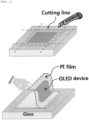
- a specific separation method may include a method of separating the carrier substrate, the polyimide layer, and the like by using a knife, laser, and the like, but is not limited thereto.
- FIG. 3 schematically illustrates a method of separating the carrier substrate below.
- the present application provides an organic light emitting device manufactured by the method of preparing the organic light emitting device.
- a flexible organic light emitting device may include: a polyimide layer; a plastic substrate formed on the polyimide layer; and an organic light emitting device formed on the plastic substrate.
- a silane coupling agent may be additionally included at least one portion between the polyimide layer and the plastic substrate.
- the silane coupling agent may serve to improve adhesion between the polyimide layer and the plastic substrate.
- a flexible organic light emitting device may include: a plastic substrate; and an organic light emitting device formed on the plastic substrate, and a silane coupling agent is included in at least one portion of a lower surface of the plastic substrate.
- the flexible organic light emitting device may include a light extraction structure. More particularly, a light extraction layer may be additionally included between the plastic substrate and the organic light emitting device.
- the light extraction layer has a structure capable of inducing light scattering, and improving light extraction efficiency of the organic light emitting device
- the light extraction layer is not particularly limited. More particularly, the light extraction layer may have a structure in which scattering particles are dispersed in a binder.
- the light extraction layer may be directly formed on a base member by a method, such as spin coating, bar coating, slit coating, and the like, or may be formed by a method of preparing the layer in a film form to be attached onto the base member.
- a planarization layer may be additionally included on the light extraction layer.
- a display device may include an organic light emitting device.
- the organic light emitting device may serve as a pixel or a backlight. Those known in the art may be applied to other configurations of the display device.
- a lighting device may include an organic light emitting device.
- the organic light emitting device serves as a light emitting part.
- Those known in the art may be applied to other configurations necessary for the lighting device.
Landscapes
- Engineering & Computer Science (AREA)
- Manufacturing & Machinery (AREA)
- Physics & Mathematics (AREA)
- Optics & Photonics (AREA)
- Electroluminescent Light Sources (AREA)
Description
- The present application relates to an organic light emitting device including a flexible substrate and a preparing method thereof.
- An organic light emitting device is formed by two opposing electrodes and organic material thin films having a plurality of layers having semiconductor-like properties interposed therebetween. The organic light emitting device having the aforementioned configuration uses a phenomenon in which electric energy is converted into light energy by using an organic material, that is, an organic light emitting phenomenon. Specifically, when voltage is applied between two electrodes in a structure in which an organic material layer is disposed between an anode and a cathode, holes from the anode and electrons from the cathode are injected into the organic material layer. When the injected holes and electrons meet each other, an exciton is formed, and the exciton falls down to a bottom state again to emit light.
- In the aforementioned organic light emitting device, light generated from the organic material layer is emitted through a light-transmitting electrode, and the organic light emitting device may be typically classified into a top emission type, a bottom-emission type, and a dual emission type. In the case of the top emission or bottom emission type, one of two electrodes needs to be a light transmitting electrode, and in the case of the dual emission type, all the two electrodes need to be light transmitting electrodes.
- In respect to the aforementioned organic light emitting device, many studies have been concentrated since Kodak Co., Ltd. announced that when a multilayer structure is used, the element may be driven at low voltage, and recently, a natural color display using the organic light emitting device is attached to a mobile phone and commercialized.
- Further, as recent studies on the organic light emitting device using a phosphorescent material instead of an existing fluorescent material have been conducted, efficiency has been rapidly improved, and it is also expected that the element would be able to replace a known lighting in the near future.
- In order to use the organic light emitting device as lighting, the element needs to be driven at high brightness unlike the existing natural color display, and constant brightness needs to be maintained like the existing lighting. In order to sufficiently improve the brightness of the organic light emitting device, light emission needs to be implemented in a large area, and in order to implement light emission in the large area, a high driving current needs to be used. In addition, in order to maintain the constant brightness in the large area, the aforementioned high current needs to be uniformly injected into the device having the large area.
-
KR 2012 0100274 A -
US 2008/0053604 A1 describes a method including the steps of preparing a carrier substrate; stacking an adhesive layer on the carrier substrate, and stacking a flexible substrate having at least one image display device on the adhesive layer using a laminating or pressing method. Thus, the flexible substrate is easily fabricated without modification of conventional mass production equipment for fabricating a display, and thereby a lightweight, thin, and compact flexible display can be realized. -
US 2011/0003442 A1 describes a method for making a flexible semiconductor device including the following steps: A rigid substrate is provided. A flexible substrate is provided, and placed on the rigid substrate. A semiconductor device is directly fromed on the flexible substrate using a semiconductor process. After the rigid substrate is removed, the flexible semiconductor device is formed. -
US 2012/0171454 A1 relates to a glass/resin laminate containing for example an organic EL element on a glass substrate and a resin layer, in which the resin layer contains a polyimide obtained by condensation-polymerization of an aromatic diamine having a benzoxazole structure with an aromatic tetracarboxylic anhydride, the difference in the average linear expansion coefficient at 25 to 300° C between the glass substrate and the resin layer is from -100×107 to +100×107/°C, and at least one outermost layer of the laminate is the glass substrate. -
US 2011/0291544 A1 describes a gas barrier substrate including a first gas barrier layer, a substrate, and a second gas barrier layer on which an OLED is provided. The first gas barrier layer has a central bonding surface bonded with the substrate and a peripheral boding surface surrounding the central bonding surface. The second gas barrier layer entirely covers the substrate and the first gas barrier layer. The second gas barrier layer is bonded with the substrate and the peripheral boding surface of the first gas barrier layer, wherein a minimum distance from an edge ofthe substrate to an edge of tlie first gas barrier layer is greater than a thickness of the first gas barrier layer. -
CN 102 629 593 describes a method for manufacturing a flexible electronic device including forming a first layer on a substrate to define a first area and a second area surrounding the first area such that the substrate is exposed at least partially in the first area and the first layer is in the second area, forming a second layer on the first area and the first layer over the second area such that an adhesion force between the second layer and the substrate in the first area is weaker than that between the second and first layers in the second area, forming an electronic device layer (EDL) on the second layer over the first area, the EDL defining a boundary projectively within the first area, and separating the EDL from the substrate by cutting through the first and second layers along a contour within the first area but not less than the boundary. - It is necessary to conduct researches on an organic light emitting device, of which process costs may be reduced by simplifying a preparing process, and which includes a substrate having a flexible property in this art.
- Accordingly, the present invention provides a method of preparing a flexible organic light emitting device according to claim 1.
- Further, a flexible organic light emitting device manufactured by the method of preparing the organic light emitting device is described.
- Further, a flexible organic light emitting is described including: a polyimide layer; a plastic substrate formed on the polyimide layer; and an organic light emitting device formed on the plastic substrate is described.
- Further, a flexible organic light emitting device, is described including: a plastic substrate: and an organic light emitting device formed on the plastic substrate, in which a silane coupling agent is included in at least one portion of a lower surface of the plastic substrate.
- Further, a display device including the flexible organic light emitting device is described.
- Further, a lighting device including the flexible organic light emitting device is described.
- According to the present application, it is possible to provide a method of preparing an organic light emitting device, of which process costs may be reduced by simplifying a preparing process, and which includes a substrate having a flexible property.
- Further, according to the present application, the process of preparing the organic light emitting device on the plastic substrate is the same as the process of preparing the organic light emitting device on the glass substrate, so that it is possible to apply the existing process as it is, and the plastic substrate is freely detachable.
-
-
FIG. 1 is a diagram schematically illustrating an inventive method of laminating a plastic substrate on a polyimide layer as an exemplary embodiment of the present application. -
FIG. 2 is a diagram schematically illustrating a cross section of an organic light emitting device formed on the plastic substrate. as an exemplary embodiment of the present application. -
FIG. 3 is a diagram schematically illustrating a preferred method of separating a carrier substrate as an exemplary embodiment of the present application. - Lightness and compactness of a product have recently become significant in a display field, but a currently used glass substrate is disadvantageously heavy, easily fragile, and difficult in a continuous process. Accordingly, researches on application of a plastic substrate, which is light, flexible, and available for a continuous process, instead of the glass substrate, to a mobile phone, a notebook computer, and a PDA, and the like have been actively conducted.
- Polyimide has an advantage in that synthesis thereof is easy, is usable for fabricating a thin film, and does not require a bridge group for hardening. Recently, according to lightness and precision of an electronic product, polyimide is widely applied to a semiconductor material, such as an LCD, a PDP, and an OLED, as an integration material. Further, many researches for using polyimide to a light and flexible plastic display substrate have been conducted, complementing disadvantages of heaviness and fragility of a glass substrate which has been used in a display field.
- In the related art, an organic light emitting device including a polyimide film requires a process of forming a polyimide film on a glass substrate, forming an organic light emitting device on the polyimide film, and then separating the organic light emitting device including the polyimide film from the glass substrate. In this case, a detaching technique of separating the organic light emitting device including the polyimide film from the glass substrate without a modification is significant.
- In general, since the polyimide film formed on the glass substrate has poor adhesion, a surface treatment with a silane coupling agent, corona, plasma, and the like needs to be performed on the glass substrate in order to enhance adhesion between the glass substrate and the polyimide film. However, there may be a problem in that it is difficult to separate the polyimide film formed on the surface-treated glass substrate later. Accordingly, in the related art, a sacrificial layer is formed under the polyimide film, or the polyimide film is separated by irradiating laser, UV, or the like.
- Further,
Japanese Patent Application Laid-Open No. 2011-142168 - Accordingly, the purpose of the present application is to provide a method of preparing an organic light emitting device, by which it is possible to decrease process costs by simplifying a preparing process, it is possible to manufacture the organic light emitting device having a large area, and the organic light emitting device may include a substrate having a flexible property.
- A method of preparing a flexible organic light emitting device according to an invenitve exemplary embodiment of the present application comprises the method steps according to claim 1.
- In the present application, step 1) is a step of forming the polyimide layer on the carrier substrate. The material known in the art may be used as the carrier substrate. More particularly, a glass substrate, a metal substrate, a plastic substrate, and the like may be used as the carrier substrate, but the carrier substrate is not limited thereto.
- The thickness of the carrier substrate may be from 0.5 mm to 0.7 mm, but is not limited thereto.
- The polyimide layer may be formed by using a method known in the art. More particularly, the polyimide layer may be formed by a process of laminating a polyimide film on a carrier substrate, and may be formed by coating a polyamic acid composition on a carrier substrate and hardening the polyamic acid composition. Further, the polyimide layer may be formed by screen-printing polyimide, but is not limited thereto.
- The polyimide layer has excellent chemical resistance and heat resistance, so that the polyimide layer may be advantageous for a photo process performed when the organic light emitting device is manufactured later.
- Step 1) may additionally include a step of patterning the polyimide layer, as long as the polyimide layer is formed only on a region of the carrier substrate on which the organic light emitting device is formed later.
- In the present application, step 2) is a step of forming the plastic substrate on the carrier substrate and the polyimide layer, wherein the plastic substrate has a wider area than that of the polyimide layer of step 1) .
- The method further includes a step of adding adhesion between the carrier substrate and the plastic substrate, and between the polyimide layer and the plastic substrate of step 2). In the step of adding the adhesion, a silane coupling agent surface treatment method, a corona surface treatment method, or a plasma surface treatment method is used on the carrier substrate and the polyimide layer. The surface treatment may be performed on an entire upper portion of the carrier substrate and the polyimide layer. The purpose of the surface treatment is to enhance adhesion between the carrier substrate and the plastic substrate.
- The plastic substrate may be selected from the group consisting of polyethylene terephthalate (PET), polyester, polycarbonate (PC), polyimide (PI), polyethylene naphthalate (PEN), polyether ether ketone (PEEK), polyarylate (PAR), polycylicolefin (PCO), polynorbornene, polyethersulphone (PEL), and cycloolefin polymer (COP), but is not limited thereto.
- More particularly, step 2) may be performed by a process of laminating the plastic substrate on the carrier substrate and the polyimide layer.
- Further, step 2) may be performed by a process of coating the polyamic acid composition on the carrier substrate and the polyimide layer and hardening the polyamic acid composition to form a polyimide film.
-
FIG. 1 schematically illustrates a method of laminating the polyimide film on photosensitive polyimide below. - The plastic substrate has a larger area than that of the polyimide layer. Further, the plastic substrate may have the same area as that of the glass substrate, but is not limited thereto. In a region of a lower portion of the plastic substrate having no polyimide layer, the plastic substrate may be directly and strongly attached to the surface treated carrier substrate, and the plastic substrate may be relatively weakly attached to the surface treated polyimide layer. The plastic substrate and the surface treated polyimide layer are relatively weakly attached to each other, so that it is possible to easily the like later. Particularly, a region of an edge region, which corresponds to a border region of the carrier substrate, having a width of 5 to 10 mm may be strongly attached with the surface treated carrier substrate and the plastic substrate.
- Further, in the region of the lower portion of the plastic substrate having no polyimide layer, the plastic substrate may be directly and strongly attached to the surface treated carrier substrate, so that it is possible to sufficiently endure a photo process, a depositing process, and the like performed when the organic light emitting device is formed later, and an adhesive property may be maintained even at a high temperature of 250°C or higher.
- In the present application, step 3) is a step of forming the organic light emitting device on the plastic substrate. The organic light emitting device may include an anode, one or more organic material layer, and a cathode.
- The anode may be formed of one or more selected from magnesium, calcium, sodium, potassium, titanium, indium, yttrium, lithium, gadolinium, aluminum, platinum, gold, tungsten, tantalum, copper, silver, tin and lead.
- In addition, the anode may also be formed of a transparent conductive oxide. Here, the transparent conductive oxide may be at least one oxide selected from indium (In), tin (Sn), zinc (Zn), gallium (Ga), cerium (Ce), cadmium (Cd), magnesium (Mg), beryllium (Be), silver (Ag), molybdenum (Mo), vanadium (V), copper (Cu), iridium (Ir), rhodium (Rh), ruthenium (Ru), tungsten (W), cobalt (Co), nickel (Ni), manganese (Mn), aluminum (Al) and lanthanum (La).
- The anode may be formed by using any one physical vapor deposition (PVD) selected from sputtering, E-beam evaporation, thermal evaporation, laser molecular beam epitaxy (L-MBE) and pulsed laser deposition (PLD); any one chemical vapor deposition selected from thermal chemical vapor deposition, plasma-enhanced chemical vapor deposition (PECVD), light chemical vapor deposition, laser chemical vapor deposition, metal-organic chemical vapor deposition (MOCVD) and hydride vapor phase epitaxy (HVPE); or atomic layer deposition (ALD).
- An auxiliary electrode may be additionally included in order to improve the resistance of the anode. The auxiliary electrode may be formed of one or more selected from the group consisting of conducting sealants and metals through a depositing process or a printing process. More particularly, the auxiliary electrode may include Cr, Mo, Al, Cu, an alloy thereof and the like, but is not limited thereto.
- An insulating layer may be additionally included on the auxiliary electrode. The insulating layer may be formed by using a material and a method known in the art. More particularly, the insulating layer may be formed by using a general photoresist material; polyimide; polyacryl; silicon nitride; silicon oxide; aluminum oxide; aluminum nitride; alkali metal oxide; alkaline earth metal oxide, and the like, but is not limited thereto. A thickness of the insulating layer may be from 10 nm to 10 µm, but is not limited thereto.
- Specific materials and formation methods for the organic material layer are not particularly limited, and materials and formation methods widely known in the art may be used.
- The organic material layer may be manufactured with fewer layers by using various polymer materials by a solvent process, for example, a spin coating method, a dip coating method, a doctor blading method, a screen printing method, an inkjet printing method, a thermal transfer method, or the like, other than a deposition method.
- The organic material layer may have a laminate structure that includes a light emitting layer, and includes one or more selected from a hole injection layer, a hole transport layer, an electron transport layer, and an electron injection layer.
- As a material capable of forming the hole injection layer, a material having a large work function is generally preferred such that the injection of holes into the organic material layer may be facilitated. Specific examples of the hole injection material include a metal, such as vanadium, chromium, copper, zinc and gold, or alloys thereof; a metal oxide, such as zinc oxide, indium oxide, indium tin oxide (ITO) and indium zinc oxide (120); a combination of metal and oxide, such as ZnO : Al or SnO2 : Sb; an electrically conductive polymer, such as poly(3-methylthiophene), poly[3,4-(ethylene-1,2-dioxy)thiophene](PEDT), polypyrrole and polyaniline, and the like, but are not limited thereto.
- As a material capable of forming the electron injection layer, a material having a small work function is generally preferred such that electrons are easily injected into the organic material layer. Specific examples of the electron injection material include a metal, such as magnesium, calcium, sodium, potassium, titanium, indium, yttrium, lithium, gadolinium, aluminum, silver, tin and lead, or alloys thereof; a multi-layered material, such as LiF/Al or LiO2/Al, and the like, and the same material as that of the hole injection electrode may be used as the electron injection material, but the electron injection material is not limited thereto.
- As layer a material capable of forming the light emitting, a material that is capable of emitting light in a visible ray region by receiving holes from the hole transport layer and electrons from the electron transport layer, respectively, and combining the holes and the electrons, and a material having high quantum efficiency for fluorescence or phosphorescence is preferable. Specific examples thereof include 8-hydroxy-quincline- aluminum complex (Alq3); carbazole-based compounds; dimerized styryl compounds; BAIq; 10-hydroxybenzoquinoline- metal compounds; benzoxazole-based, benzthiazole-based and benzimidazole-based compounds; poly(p-phenylenevinylene)(PPV)-based polymers; spiro compounds; polyfluorene and rubrene; phosphorescence host CBP[[4,4'-bis(9-carbazolyl)biphenyl] and the like, but are not limited thereto.
- Further, the light emitting material may additionally include a phosphorescent dopant or fluorescent dopant in order to improve fluorescent or phosphorescent characteristics. Specific examples of the phosphorescent dopant include ir(ppy)(3) [fac tris(2-phenylpyridine) iridium], F2lrpic [iridium(III)bis(4,6,-di-fluorophenyl-pyridinato-N,C2) picolinate] or the like. As the fluorescent dopant, those known in the art may be used.
- As a material capable of forming the electron transport layer, a material capable of receiving electrons from the electron injection layer well and transporting the electrons to the light emitting layer, and having high mobility to electrons is suitable. Specific examples thereof include Al complexes of 8-hydroxyquinoline; complexes including Alq3; organic radical compounds; hydroxyflavone-metal complexes; and the like, but are not limited thereto.
- The cathode may include at least one of Al, Ag, Ca, Mg, Au, Mo, Ir, Cr, Ti, Pd, and an alloy thereof, but is not limited thereto.
-
FIG. 2 schematically illustrates a cross section of the organic light emitting device formed on the plastic substrate. - A step of encapsulating the organic light emitting device may be additionally included after step 3). The purpose of the encapsulation is to prevent foreign substances, such as oxygen and moisture, from permeating into the organic light emitting device, and may be performed by using a material, a method, and the like known in the art.
- The encapsulation process may be performed by forming a sealing part covering an external side of the organic light emitting device.
- If the sealing part may seal the organic light emitting device while covering the external side of the organic light emitting device, a material thereof is not particularly limited. For example, the sealing part may be formed by compressing the external side of the organic light emitting device with a sealing film, or depositing a metal or a metal oxide, or may be formed by coating and hardening a resin composition.
- Further, the sealing part may be formed by depositing a metal or a metal oxide by an atomic layer deposition method. Here, the formed metal layer or metal oxide layer may be a structure having two or more layers.
- Step 4) is a step of separating the carrier substrate.
- In the related art, it is difficult to separate a polyimide film formed on a surface treated carrier substrate, so that a sacrificial layer is formed under the polyimide film, or the polyimide film is separated by irradiating laser, UV, or the like. However, in the present application, in the region of the lower portion of the plastic substrate having no polyimide layer, the plastic substrate is directly and strongly attached to the surface treated carrier substrate, and the plastic substrate is relatively weakly attached to the surface treated polyimide layer by using the patterned polyimide layer, so that it is possible to easily separate the carrier substrate, the polyimide layer, and the like. A specific separation method may include a method of separating the carrier substrate, the polyimide layer, and the like by using a knife, laser, and the like, but is not limited thereto.
-
FIG. 3 schematically illustrates a method of separating the carrier substrate below. - Further, the present application provides an organic light emitting device manufactured by the method of preparing the organic light emitting device.
- Further, a flexible organic light emitting device may include: a polyimide layer; a plastic substrate formed on the polyimide layer; and an organic light emitting device formed on the plastic substrate.
- In the present application, a silane coupling agent may be additionally included at least one portion between the polyimide layer and the plastic substrate. The silane coupling agent may serve to improve adhesion between the polyimide layer and the plastic substrate.
- Further, a flexible organic light emitting device according may include: a plastic substrate; and an organic light emitting device formed on the plastic substrate, and a silane coupling agent is included in at least one portion of a lower surface of the plastic substrate.
- In a flexible organic light emitting device, contents of the polyimide layer, the plastic substrate, the organic light emitting device, and the like are the same as those in the above description, so that detailed descriptions thereof will be omitted.
- The flexible organic light emitting device may include a light extraction structure. More particularly, a light extraction layer may be additionally included between the plastic substrate and the organic light emitting device.
- If the light extraction layer has a structure capable of inducing light scattering, and improving light extraction efficiency of the organic light emitting device, the light extraction layer is not particularly limited. More particularly, the light extraction layer may have a structure in which scattering particles are dispersed in a binder.
- Further, the light extraction layer may be directly formed on a base member by a method, such as spin coating, bar coating, slit coating, and the like, or may be formed by a method of preparing the layer in a film form to be attached onto the base member.
- Further, a planarization layer may be additionally included on the light extraction layer.
- A display device may include an organic light emitting device. In the display device, the organic light emitting device may serve as a pixel or a backlight. Those known in the art may be applied to other configurations of the display device.
- A lighting device may include an organic light emitting device. In the lighting device, the organic light emitting device serves as a light emitting part. Those known in the art may be applied to other configurations necessary for the lighting device.
- As described above, according to the present application, it is possible to provide a method for preparing a flexible organic light emitting device, of which process costs may be reduced by simplifying a preparing process, and includes a substrate having a flexible property.
Claims (11)
- A method for preparing a flexible organic light emitting device, comprising:1) forming a polyimide layer only on a region of a carrier substrate on which the organic light emitting device is formed later;2) adding adhesion between the carrier substrate and a plastic substrate, and between the polyimide layer and the plastic substrate and forming the plastic substrate on the carrier substrate and the polyimide layer,
wherein the plastic substrate of step 2) has a wider area than that of the polyimide layer of step 1),3) forming an organic light emitting device on the plastic substrate; and4) characterized by separating the carrier substrate and the polyimide layer from the plastic substrate and in that adding of the adhesion in step 2) uses a silane coupling agent surface treatment method, a corona surface treatment method, or a plasma surface treatment method on the carrier substrate and the polyimide layer. - The method of claim 1, wherein the polyimide layer of step 1) is formed by coating and hardening a polyamic acid composition.
- The method of claim 1, wherein the carrier substrate is a glass substrate, a metal substrate, or a plastic substrate.
- The method of claim 1, wherein a thickness of the carrier substrate is from 0.5 to 0.7 mm.
- The method of claim 1, wherein step 2) is performed by a process of laminating the plastic substrate on the carrier substrate and the polyimide layer.
- The method of claim 1, wherein the plastic substrate is selected from the group consisting of polyethylene terephthalate (PET), polyester, polycarbonate (PC), polyimide (PI), polyethylene naphthalate (PEN), polyether ether ketone (PEEK), polyarylate (PAR), polycyclicolefin (PCO), polynorbornene, polyethersulphone (PES), and cycloolefin polymer (COP).
- The method of claim 1, wherein the plastic substrate includes a polyimide film, and step 2) is performed by a process of a coating polyamic acid composition on the carrier substrate and the polyimide layer and hardening the polyamic acid composition to form the polyimide film.
- The method of claim 1, wherein the plastic substrate of step 2) has the same area as that of the carrier substrate.
- The method of claim 1, further comprising:
encapsulating the organic light emitting device after step 3). - The method of claim 1, wherein a method of separating the carrier substrate of step 4) uses a knife or laser.
- The method of claim 1, further comprising:
removing the polyimide layer simultaneously with or after step 4) .
Applications Claiming Priority (2)
| Application Number | Priority Date | Filing Date | Title |
|---|---|---|---|
| KR20120138336 | 2012-11-30 | ||
| PCT/KR2013/010398 WO2014084529A1 (en) | 2012-11-30 | 2013-11-15 | Organic light-emitting device including flexible substrate, and method for manufacturing same |
Publications (3)
| Publication Number | Publication Date |
|---|---|
| EP2927982A1 EP2927982A1 (en) | 2015-10-07 |
| EP2927982A4 EP2927982A4 (en) | 2016-12-07 |
| EP2927982B1 true EP2927982B1 (en) | 2024-05-08 |
Family
ID=50828109
Family Applications (1)
| Application Number | Title | Priority Date | Filing Date |
|---|---|---|---|
| EP13857827.3A Active EP2927982B1 (en) | 2012-11-30 | 2013-11-15 | Organic light-emitting device including flexible substrate, and method for manufacturing same |
Country Status (7)
| Country | Link |
|---|---|
| US (1) | US9871228B2 (en) |
| EP (1) | EP2927982B1 (en) |
| JP (1) | JP6417330B2 (en) |
| KR (1) | KR101445044B1 (en) |
| CN (1) | CN104854722B (en) |
| TW (1) | TWI523295B (en) |
| WO (1) | WO2014084529A1 (en) |
Families Citing this family (32)
| Publication number | Priority date | Publication date | Assignee | Title |
|---|---|---|---|---|
| KR102361966B1 (en) | 2013-12-02 | 2022-02-14 | 가부시키가이샤 한도오따이 에네루기 켄큐쇼 | Display device and method for manufacturing the same |
| KR102312462B1 (en) * | 2014-07-17 | 2021-10-13 | 아사히 가세이 가부시키가이샤 | Resin precursor, resin composition containing same, polyimide resin membrane, resin film, and method for producing same |
| CN104362263A (en) * | 2014-10-31 | 2015-02-18 | 华南理工大学 | Flexible membrane liner and substrate separation process for producing flexible display device |
| KR101661619B1 (en) | 2014-11-05 | 2016-09-30 | 율촌화학 주식회사 | Gas inducing adhesive film, flexible display including thereof, and method of manufacturing flexible display device using thereof |
| KR20160064747A (en) * | 2014-11-28 | 2016-06-08 | 동우 화인켐 주식회사 | Touch sensor associated with upper plate of lcd panel |
| CN105789440A (en) * | 2014-12-23 | 2016-07-20 | 深圳Tcl工业研究院有限公司 | Composite substrate for fabricating flexible display, fabrication method of composite substrate and fabrication method of active matrix/organic light emitting diode (AMOLED) |
| TWI542923B (en) * | 2015-03-09 | 2016-07-21 | 友達光電股份有限公司 | Flexible display panel and manufacturing method thereof |
| JP6735554B2 (en) * | 2015-12-10 | 2020-08-05 | エルジー ディスプレイ カンパニー リミテッド | Flexible organic EL display device and manufacturing method thereof |
| US10586817B2 (en) | 2016-03-24 | 2020-03-10 | Semiconductor Energy Laboratory Co., Ltd. | Semiconductor device, manufacturing method thereof, and separation apparatus |
| US10003023B2 (en) | 2016-04-15 | 2018-06-19 | Semiconductor Energy Laboratory Co., Ltd. | Display device and electronic device |
| US10185190B2 (en) | 2016-05-11 | 2019-01-22 | Semiconductor Energy Laboratory Co., Ltd. | Display device, module, and electronic device |
| KR20230106750A (en) | 2016-07-29 | 2023-07-13 | 가부시키가이샤 한도오따이 에네루기 켄큐쇼 | Separation method, display device, display module, and electronic device |
| TWI753868B (en) | 2016-08-05 | 2022-02-01 | 日商半導體能源研究所股份有限公司 | Peeling method, display device, display module and electronic device |
| TW201808628A (en) | 2016-08-09 | 2018-03-16 | 半導體能源研究所股份有限公司 | Semiconductor device manufacturing method |
| TWI730017B (en) | 2016-08-09 | 2021-06-11 | 日商半導體能源研究所股份有限公司 | Manufacturing method of display device, display device, display module and electronic device |
| TWI629770B (en) * | 2016-08-09 | 2018-07-11 | Usun Technology Co., Ltd. | Method for separating flexible display from carrier substrate |
| JP6981812B2 (en) | 2016-08-31 | 2021-12-17 | 株式会社半導体エネルギー研究所 | Manufacturing method of semiconductor device |
| KR102425705B1 (en) | 2016-08-31 | 2022-07-28 | 가부시키가이샤 한도오따이 에네루기 켄큐쇼 | Method of manufacturing a semiconductor device |
| US10369664B2 (en) | 2016-09-23 | 2019-08-06 | Semiconductor Energy Laboratory Co., Ltd. | Manufacturing method of semiconductor device |
| KR102630960B1 (en) * | 2016-12-15 | 2024-01-29 | 엘지디스플레이 주식회사 | Flexible substrate, flexible display device including the same, and manufacturing method thereof |
| JP6878870B2 (en) * | 2016-12-20 | 2021-06-02 | 東洋紡株式会社 | Laminates, methods for manufacturing laminates and methods for manufacturing flexible devices |
| KR102008766B1 (en) | 2017-01-31 | 2019-08-09 | 주식회사 엘지화학 | Laminate for manufacturing flexible substrate and process for manufacturing flexible substrate using same |
| CN107195658B (en) * | 2017-05-25 | 2020-01-21 | 上海天马微电子有限公司 | Flexible substrate and manufacturing method thereof |
| CN107464893A (en) * | 2017-07-31 | 2017-12-12 | 武汉华星光电半导体显示技术有限公司 | Preparation method, flexible display device and the display of flexible display device |
| US10658592B2 (en) | 2017-07-31 | 2020-05-19 | Wuhan China Star Optoelectronics Semiconductor Display Technology Co., Ltd. | Method for fabricating flexible display device, flexible display device, and display apparatus |
| US10811609B2 (en) | 2017-09-06 | 2020-10-20 | Sharp Kabushiki Kaisha | Manufacturing method of display device |
| CN111433020B (en) * | 2018-09-11 | 2022-11-15 | 株式会社Lg化学 | Laminate for manufacturing flexible display and flexible display manufacturing method using same |
| KR102696647B1 (en) | 2018-11-09 | 2024-08-22 | 삼성디스플레이 주식회사 | Flexible display apparatus and manufacturing method thereof |
| CN110132315A (en) * | 2019-04-08 | 2019-08-16 | 清华大学深圳研究生院 | A kind of flexible sensor and preparation method thereof and wearable smart machine |
| CN110739337B (en) * | 2019-10-24 | 2022-06-17 | 云谷(固安)科技有限公司 | Flexible substrate, display panel and preparation method of display panel |
| CN111755632B (en) * | 2020-07-30 | 2022-07-19 | 河南工程学院 | A kind of flexible organic electroluminescent device and preparation method thereof |
| CN116917660A (en) * | 2021-02-25 | 2023-10-20 | 东友精细化工有限公司 | LED lighting device and manufacturing method thereof |
Citations (1)
| Publication number | Priority date | Publication date | Assignee | Title |
|---|---|---|---|---|
| CN102629593A (en) * | 2011-11-09 | 2012-08-08 | 友达光电股份有限公司 | Flexible electronic device and manufacturing method thereof |
Family Cites Families (38)
| Publication number | Priority date | Publication date | Assignee | Title |
|---|---|---|---|---|
| JP4841103B2 (en) | 2000-06-16 | 2011-12-21 | ユニチカ株式会社 | Manufacturing method of flexible printed wiring board substrate and flexible printed wiring board substrate |
| JP2002198374A (en) * | 2000-10-16 | 2002-07-12 | Sharp Corp | Semiconductor device and method of manufacturing the same |
| US8057903B2 (en) | 2001-11-30 | 2011-11-15 | Sabic Innovative Plastics Ip B.V. | Multilayer articles comprising resorcinol arylate polyester and method for making thereof |
| US20060043343A1 (en) * | 2004-08-24 | 2006-03-02 | Chacko Antony P | Polymer composition and film having positive temperature coefficient |
| DE102006055067B4 (en) * | 2005-12-29 | 2017-04-20 | Lg Display Co., Ltd. | Organic thin film transistors and process for their manufacture |
| KR100820170B1 (en) | 2006-08-30 | 2008-04-10 | 한국전자통신연구원 | Stacking method of flexible substrate |
| KR101330456B1 (en) * | 2006-12-12 | 2013-11-15 | 엘지디스플레이 주식회사 | Equipment for manufacturing flexible display and method for manufacturing flexible display by using the same |
| JP5150138B2 (en) * | 2007-05-23 | 2013-02-20 | 株式会社ジャパンディスプレイイースト | Manufacturing method of display device |
| US7674689B2 (en) * | 2007-09-20 | 2010-03-09 | Infineon Technologies Ag | Method of making an integrated circuit including singulating a semiconductor wafer |
| KR20090096365A (en) * | 2008-03-07 | 2009-09-10 | 주식회사 엘지화학 | Positive photosensitive polyimide composition |
| KR20100138939A (en) | 2008-03-18 | 2010-12-31 | 아사히 가라스 가부시키가이샤 | Electronic device board | substrate, laminated body for organic LED elements, its manufacturing method, organic LED element, and its manufacturing method |
| KR101500684B1 (en) * | 2008-04-17 | 2015-03-10 | 삼성디스플레이 주식회사 | Carrier substrate and method of manufacturing flexible display device using same |
| JP2009283155A (en) | 2008-05-19 | 2009-12-03 | Seiko Epson Corp | Manufacturing method of display device, display device, and electronic apparatus |
| TWI354854B (en) | 2008-09-15 | 2011-12-21 | Ind Tech Res Inst | Substrate structures applied in flexible electrica |
| KR101009415B1 (en) | 2008-11-18 | 2011-01-19 | 삼성모바일디스플레이주식회사 | A method of manufacturing an electronic device having a plastic substrate, an electronic device manufactured thereby, and a device used in the manufacturing method |
| EP2366270A4 (en) * | 2008-12-02 | 2013-04-10 | Univ Arizona | PROCESS FOR PREPARING A SOFT SUBSTRATE AND SOFT SUBSTRATE THUS OBTAINED |
| US8273439B2 (en) | 2008-12-08 | 2012-09-25 | Industrial Technology Research Institute | Release layer materials, substrate structures comprising the same and fabrication method thereof |
| KR101319170B1 (en) | 2008-12-19 | 2013-10-16 | 도요보 가부시키가이샤 | Laminated body, manufacturing method thereof, and laminated circuit board |
| KR101029299B1 (en) * | 2008-12-30 | 2011-04-18 | 서울대학교산학협력단 | Organic light emitting device and method for manufacturing same |
| WO2010093013A1 (en) * | 2009-02-13 | 2010-08-19 | 学校法人東京工芸大学 | Image display device and organic electroluminescent element |
| TWI421809B (en) * | 2009-04-17 | 2014-01-01 | 財團法人工業技術研究院 | Method for detaching flexible substrate from carrier and method for manufacturing flexible electronic device |
| TWI439976B (en) * | 2009-04-17 | 2014-06-01 | Ind Tech Res Inst | Method for isolating a flexible film from a substrate and method for fabricating an electric device |
| CN101944477B (en) * | 2009-07-03 | 2012-06-20 | 清华大学 | Manufacturing method for flexible semiconductor device |
| CN102481764B (en) * | 2009-09-08 | 2014-11-05 | 旭硝子株式会社 | Glass/resin laminate, and electronic device using same |
| EA201270559A1 (en) * | 2009-10-15 | 2012-11-30 | Асахи Гласс Компани, Лимитед | ORGANIC LED ELEMENT, FRITTATED GLASS FOR SCATTERING LAYER FOR APPLICATION IN ORGANIC LED ELEMENT AND METHOD FOR OBTAINING DIFFUSION LAYER FOR APPLICATION IN ORGANIC LED ELEMENT |
| JP2011142168A (en) | 2010-01-06 | 2011-07-21 | Fujifilm Corp | Method of manufacturing electronic device, and substrate used for the electronic device |
| US8538224B2 (en) * | 2010-04-22 | 2013-09-17 | 3M Innovative Properties Company | OLED light extraction films having internal nanostructures and external microstructures |
| KR101145724B1 (en) | 2010-05-04 | 2012-05-16 | 부산대학교 산학협력단 | Organic light emitting device to enhance out coupling efficiency and method of preparing the device |
| US20110291544A1 (en) * | 2010-05-31 | 2011-12-01 | Industrial Technology Research Institute | Gas barrier substrate, package of organic electro-luminenscent device and packaging method thereof |
| KR101783781B1 (en) * | 2010-07-05 | 2017-10-11 | 삼성디스플레이 주식회사 | A flat display device and the manufacturing method thereof |
| KR101845440B1 (en) | 2010-11-18 | 2018-04-04 | 엘지디스플레이 주식회사 | Method for Manufacturing Flexible Display Device |
| TW201228807A (en) * | 2011-01-13 | 2012-07-16 | Moser Baer India Ltd | Method of imprinting a texture on a rigid substrate using flexible stamp |
| JP2012178268A (en) * | 2011-02-25 | 2012-09-13 | Mitsubishi Chemicals Corp | Organic electroluminescent element, organic electroluminescent module, organic electroluminescent display device, and organic electroluminescent illumination device |
| KR101918284B1 (en) * | 2011-03-03 | 2019-01-30 | 엘지디스플레이 주식회사 | Method of manufacturing a flexible display device |
| JP5355618B2 (en) * | 2011-03-10 | 2013-11-27 | 三星ディスプレイ株式會社 | Flexible display device and manufacturing method thereof |
| TWI445626B (en) | 2011-03-18 | 2014-07-21 | 長興化學工業股份有限公司 | Method of manufacturing a flexible component |
| JP5906574B2 (en) * | 2011-03-29 | 2016-04-20 | 大日本印刷株式会社 | Flexible device substrate and manufacturing method thereof |
| KR101433555B1 (en) | 2011-04-15 | 2014-08-22 | 도요보 가부시키가이샤 | Laminate, method for producing same, and method for producing device structure using same |
-
2013
- 2013-11-15 CN CN201380062613.1A patent/CN104854722B/en active Active
- 2013-11-15 JP JP2015545352A patent/JP6417330B2/en active Active
- 2013-11-15 KR KR1020130139112A patent/KR101445044B1/en active Active
- 2013-11-15 WO PCT/KR2013/010398 patent/WO2014084529A1/en not_active Ceased
- 2013-11-15 TW TW102141682A patent/TWI523295B/en active
- 2013-11-15 US US14/647,758 patent/US9871228B2/en active Active
- 2013-11-15 EP EP13857827.3A patent/EP2927982B1/en active Active
Patent Citations (2)
| Publication number | Priority date | Publication date | Assignee | Title |
|---|---|---|---|---|
| CN102629593A (en) * | 2011-11-09 | 2012-08-08 | 友达光电股份有限公司 | Flexible electronic device and manufacturing method thereof |
| EP2592653A1 (en) * | 2011-11-09 | 2013-05-15 | AU Optronics Corporation | Method of manufacturing flexible electronic device |
Also Published As
| Publication number | Publication date |
|---|---|
| WO2014084529A1 (en) | 2014-06-05 |
| US9871228B2 (en) | 2018-01-16 |
| JP2015536555A (en) | 2015-12-21 |
| EP2927982A1 (en) | 2015-10-07 |
| KR20140076485A (en) | 2014-06-20 |
| TWI523295B (en) | 2016-02-21 |
| EP2927982A4 (en) | 2016-12-07 |
| KR101445044B1 (en) | 2014-09-26 |
| CN104854722A (en) | 2015-08-19 |
| TW201432977A (en) | 2014-08-16 |
| US20150303408A1 (en) | 2015-10-22 |
| CN104854722B (en) | 2017-09-22 |
| JP6417330B2 (en) | 2018-11-07 |
Similar Documents
| Publication | Publication Date | Title |
|---|---|---|
| US9871228B2 (en) | Organic light emitting device comprising flexible substrate and method for preparing thereof | |
| JP6336569B2 (en) | ORGANIC LIGHT-EMITTING ELEMENT AND MANUFACTURING METHOD | |
| JP6343026B2 (en) | LAMINATED FOR SEALING, ORGANIC LIGHT EMITTING DEVICE AND METHOD FOR PRODUCING THEM | |
| EP2592672B1 (en) | Organic light-emitting device and method for manufacturing same | |
| EP3018724B1 (en) | Organic light-emitting device and manufacturing method therefor | |
| US10153454B2 (en) | Organic light-emitting element and production method thereof | |
| EP3016161B1 (en) | Organic light emitting device | |
| JPH11312584A (en) | Organic EL device | |
| KR101314452B1 (en) | Organic light emitting device and manufacturing method thereof | |
| KR101806940B1 (en) | Organic light emitting device and method for preparing the same | |
| KR101947381B1 (en) | Method for preparing flexible substrate and method for preparing organic light emitting device comprising the same | |
| EP3018725B1 (en) | Method for manufacturing organic light-emitting device | |
| KR101752337B1 (en) | Organic light emitting device and method for preparing the same | |
| KR101677425B1 (en) | Organic light emitting device and method for preparing the same | |
| KR20150035262A (en) | Organic light emitting device and method for preparing thereof | |
| JPWO2016072246A1 (en) | Organic electroluminescence device | |
| KR20150037025A (en) | Organic light emitting device comprising flexible substrate and method for preparing thereof | |
| KR20150024189A (en) | Method for preparing flexible substrate and method for preparing organic light emitting device comprising the same |
Legal Events
| Date | Code | Title | Description |
|---|---|---|---|
| PUAI | Public reference made under article 153(3) epc to a published international application that has entered the european phase |
Free format text: ORIGINAL CODE: 0009012 |
|
| 17P | Request for examination filed |
Effective date: 20150611 |
|
| AK | Designated contracting states |
Kind code of ref document: A1 Designated state(s): AL AT BE BG CH CY CZ DE DK EE ES FI FR GB GR HR HU IE IS IT LI LT LU LV MC MK MT NL NO PL PT RO RS SE SI SK SM TR |
|
| AX | Request for extension of the european patent |
Extension state: BA ME |
|
| DAX | Request for extension of the european patent (deleted) | ||
| RAP1 | Party data changed (applicant data changed or rights of an application transferred) |
Owner name: LG DISPLAY CO., LTD. |
|
| RIC1 | Information provided on ipc code assigned before grant |
Ipc: H01L 51/56 20060101ALI20160531BHEP Ipc: H01L 51/50 20060101AFI20160531BHEP |
|
| RA4 | Supplementary search report drawn up and despatched (corrected) |
Effective date: 20161107 |
|
| RIC1 | Information provided on ipc code assigned before grant |
Ipc: H01L 51/52 20060101AFI20161031BHEP |
|
| STAA | Information on the status of an ep patent application or granted ep patent |
Free format text: STATUS: EXAMINATION IS IN PROGRESS |
|
| 17Q | First examination report despatched |
Effective date: 20200221 |
|
| REG | Reference to a national code |
Ref country code: DE Ref legal event code: R079 Free format text: PREVIOUS MAIN CLASS: H01L0051500000 Ipc: H10K0071800000 Ref country code: DE Ref legal event code: R079 Ref document number: 602013085697 Country of ref document: DE Free format text: PREVIOUS MAIN CLASS: H01L0051500000 Ipc: H10K0071800000 |
|
| GRAP | Despatch of communication of intention to grant a patent |
Free format text: ORIGINAL CODE: EPIDOSNIGR1 |
|
| STAA | Information on the status of an ep patent application or granted ep patent |
Free format text: STATUS: GRANT OF PATENT IS INTENDED |
|
| RIC1 | Information provided on ipc code assigned before grant |
Ipc: B32B 17/10 20060101ALI20231211BHEP Ipc: B32B 7/06 20060101ALI20231211BHEP Ipc: H10K 77/10 20230101ALI20231211BHEP Ipc: H10K 71/80 20230101AFI20231211BHEP |
|
| INTG | Intention to grant announced |
Effective date: 20240112 |
|
| GRAS | Grant fee paid |
Free format text: ORIGINAL CODE: EPIDOSNIGR3 |
|
| GRAA | (expected) grant |
Free format text: ORIGINAL CODE: 0009210 |
|
| STAA | Information on the status of an ep patent application or granted ep patent |
Free format text: STATUS: THE PATENT HAS BEEN GRANTED |
|
| AK | Designated contracting states |
Kind code of ref document: B1 Designated state(s): AL AT BE BG CH CY CZ DE DK EE ES FI FR GB GR HR HU IE IS IT LI LT LU LV MC MK MT NL NO PL PT RO RS SE SI SK SM TR |
|
| REG | Reference to a national code |
Ref country code: GB Ref legal event code: FG4D |
|
| REG | Reference to a national code |
Ref country code: CH Ref legal event code: EP |
|
| REG | Reference to a national code |
Ref country code: DE Ref legal event code: R096 Ref document number: 602013085697 Country of ref document: DE |
|
| REG | Reference to a national code |
Ref country code: IE Ref legal event code: FG4D |
|
| REG | Reference to a national code |
Ref country code: LT Ref legal event code: MG9D |
|
| REG | Reference to a national code |
Ref country code: NL Ref legal event code: MP Effective date: 20240508 |
|
| PG25 | Lapsed in a contracting state [announced via postgrant information from national office to epo] |
Ref country code: IS Free format text: LAPSE BECAUSE OF FAILURE TO SUBMIT A TRANSLATION OF THE DESCRIPTION OR TO PAY THE FEE WITHIN THE PRESCRIBED TIME-LIMIT Effective date: 20240908 |
|
| PG25 | Lapsed in a contracting state [announced via postgrant information from national office to epo] |
Ref country code: BG Free format text: LAPSE BECAUSE OF FAILURE TO SUBMIT A TRANSLATION OF THE DESCRIPTION OR TO PAY THE FEE WITHIN THE PRESCRIBED TIME-LIMIT Effective date: 20240508 |
|
| PG25 | Lapsed in a contracting state [announced via postgrant information from national office to epo] |
Ref country code: HR Free format text: LAPSE BECAUSE OF FAILURE TO SUBMIT A TRANSLATION OF THE DESCRIPTION OR TO PAY THE FEE WITHIN THE PRESCRIBED TIME-LIMIT Effective date: 20240508 Ref country code: FI Free format text: LAPSE BECAUSE OF FAILURE TO SUBMIT A TRANSLATION OF THE DESCRIPTION OR TO PAY THE FEE WITHIN THE PRESCRIBED TIME-LIMIT Effective date: 20240508 |
|
| PG25 | Lapsed in a contracting state [announced via postgrant information from national office to epo] |
Ref country code: GR Free format text: LAPSE BECAUSE OF FAILURE TO SUBMIT A TRANSLATION OF THE DESCRIPTION OR TO PAY THE FEE WITHIN THE PRESCRIBED TIME-LIMIT Effective date: 20240809 |
|
| PG25 | Lapsed in a contracting state [announced via postgrant information from national office to epo] |
Ref country code: PT Free format text: LAPSE BECAUSE OF FAILURE TO SUBMIT A TRANSLATION OF THE DESCRIPTION OR TO PAY THE FEE WITHIN THE PRESCRIBED TIME-LIMIT Effective date: 20240909 |
|
| REG | Reference to a national code |
Ref country code: AT Ref legal event code: MK05 Ref document number: 1686077 Country of ref document: AT Kind code of ref document: T Effective date: 20240508 |
|
| PG25 | Lapsed in a contracting state [announced via postgrant information from national office to epo] |
Ref country code: NL Free format text: LAPSE BECAUSE OF FAILURE TO SUBMIT A TRANSLATION OF THE DESCRIPTION OR TO PAY THE FEE WITHIN THE PRESCRIBED TIME-LIMIT Effective date: 20240508 |
|
| PG25 | Lapsed in a contracting state [announced via postgrant information from national office to epo] |
Ref country code: ES Free format text: LAPSE BECAUSE OF FAILURE TO SUBMIT A TRANSLATION OF THE DESCRIPTION OR TO PAY THE FEE WITHIN THE PRESCRIBED TIME-LIMIT Effective date: 20240508 |
|
| PG25 | Lapsed in a contracting state [announced via postgrant information from national office to epo] |
Ref country code: AT Free format text: LAPSE BECAUSE OF FAILURE TO SUBMIT A TRANSLATION OF THE DESCRIPTION OR TO PAY THE FEE WITHIN THE PRESCRIBED TIME-LIMIT Effective date: 20240508 |
|
| PG25 | Lapsed in a contracting state [announced via postgrant information from national office to epo] |
Ref country code: PL Free format text: LAPSE BECAUSE OF FAILURE TO SUBMIT A TRANSLATION OF THE DESCRIPTION OR TO PAY THE FEE WITHIN THE PRESCRIBED TIME-LIMIT Effective date: 20240508 |
|
| PG25 | Lapsed in a contracting state [announced via postgrant information from national office to epo] |
Ref country code: LV Free format text: LAPSE BECAUSE OF FAILURE TO SUBMIT A TRANSLATION OF THE DESCRIPTION OR TO PAY THE FEE WITHIN THE PRESCRIBED TIME-LIMIT Effective date: 20240508 |
|
| PG25 | Lapsed in a contracting state [announced via postgrant information from national office to epo] |
Ref country code: PT Free format text: LAPSE BECAUSE OF FAILURE TO SUBMIT A TRANSLATION OF THE DESCRIPTION OR TO PAY THE FEE WITHIN THE PRESCRIBED TIME-LIMIT Effective date: 20240909 Ref country code: PL Free format text: LAPSE BECAUSE OF FAILURE TO SUBMIT A TRANSLATION OF THE DESCRIPTION OR TO PAY THE FEE WITHIN THE PRESCRIBED TIME-LIMIT Effective date: 20240508 Ref country code: NO Free format text: LAPSE BECAUSE OF FAILURE TO SUBMIT A TRANSLATION OF THE DESCRIPTION OR TO PAY THE FEE WITHIN THE PRESCRIBED TIME-LIMIT Effective date: 20240808 Ref country code: NL Free format text: LAPSE BECAUSE OF FAILURE TO SUBMIT A TRANSLATION OF THE DESCRIPTION OR TO PAY THE FEE WITHIN THE PRESCRIBED TIME-LIMIT Effective date: 20240508 Ref country code: LV Free format text: LAPSE BECAUSE OF FAILURE TO SUBMIT A TRANSLATION OF THE DESCRIPTION OR TO PAY THE FEE WITHIN THE PRESCRIBED TIME-LIMIT Effective date: 20240508 Ref country code: IS Free format text: LAPSE BECAUSE OF FAILURE TO SUBMIT A TRANSLATION OF THE DESCRIPTION OR TO PAY THE FEE WITHIN THE PRESCRIBED TIME-LIMIT Effective date: 20240908 Ref country code: HR Free format text: LAPSE BECAUSE OF FAILURE TO SUBMIT A TRANSLATION OF THE DESCRIPTION OR TO PAY THE FEE WITHIN THE PRESCRIBED TIME-LIMIT Effective date: 20240508 Ref country code: GR Free format text: LAPSE BECAUSE OF FAILURE TO SUBMIT A TRANSLATION OF THE DESCRIPTION OR TO PAY THE FEE WITHIN THE PRESCRIBED TIME-LIMIT Effective date: 20240809 Ref country code: FI Free format text: LAPSE BECAUSE OF FAILURE TO SUBMIT A TRANSLATION OF THE DESCRIPTION OR TO PAY THE FEE WITHIN THE PRESCRIBED TIME-LIMIT Effective date: 20240508 Ref country code: ES Free format text: LAPSE BECAUSE OF FAILURE TO SUBMIT A TRANSLATION OF THE DESCRIPTION OR TO PAY THE FEE WITHIN THE PRESCRIBED TIME-LIMIT Effective date: 20240508 Ref country code: BG Free format text: LAPSE BECAUSE OF FAILURE TO SUBMIT A TRANSLATION OF THE DESCRIPTION OR TO PAY THE FEE WITHIN THE PRESCRIBED TIME-LIMIT Effective date: 20240508 Ref country code: AT Free format text: LAPSE BECAUSE OF FAILURE TO SUBMIT A TRANSLATION OF THE DESCRIPTION OR TO PAY THE FEE WITHIN THE PRESCRIBED TIME-LIMIT Effective date: 20240508 Ref country code: RS Free format text: LAPSE BECAUSE OF FAILURE TO SUBMIT A TRANSLATION OF THE DESCRIPTION OR TO PAY THE FEE WITHIN THE PRESCRIBED TIME-LIMIT Effective date: 20240808 |
|
| PG25 | Lapsed in a contracting state [announced via postgrant information from national office to epo] |
Ref country code: DK Free format text: LAPSE BECAUSE OF FAILURE TO SUBMIT A TRANSLATION OF THE DESCRIPTION OR TO PAY THE FEE WITHIN THE PRESCRIBED TIME-LIMIT Effective date: 20240508 |
|
| PG25 | Lapsed in a contracting state [announced via postgrant information from national office to epo] |
Ref country code: EE Free format text: LAPSE BECAUSE OF FAILURE TO SUBMIT A TRANSLATION OF THE DESCRIPTION OR TO PAY THE FEE WITHIN THE PRESCRIBED TIME-LIMIT Effective date: 20240508 |
|
| PG25 | Lapsed in a contracting state [announced via postgrant information from national office to epo] |
Ref country code: CZ Free format text: LAPSE BECAUSE OF FAILURE TO SUBMIT A TRANSLATION OF THE DESCRIPTION OR TO PAY THE FEE WITHIN THE PRESCRIBED TIME-LIMIT Effective date: 20240508 |
|
| PG25 | Lapsed in a contracting state [announced via postgrant information from national office to epo] |
Ref country code: SK Free format text: LAPSE BECAUSE OF FAILURE TO SUBMIT A TRANSLATION OF THE DESCRIPTION OR TO PAY THE FEE WITHIN THE PRESCRIBED TIME-LIMIT Effective date: 20240508 Ref country code: RO Free format text: LAPSE BECAUSE OF FAILURE TO SUBMIT A TRANSLATION OF THE DESCRIPTION OR TO PAY THE FEE WITHIN THE PRESCRIBED TIME-LIMIT Effective date: 20240508 |
|
| PG25 | Lapsed in a contracting state [announced via postgrant information from national office to epo] |
Ref country code: SM Free format text: LAPSE BECAUSE OF FAILURE TO SUBMIT A TRANSLATION OF THE DESCRIPTION OR TO PAY THE FEE WITHIN THE PRESCRIBED TIME-LIMIT Effective date: 20240508 |
|
| PG25 | Lapsed in a contracting state [announced via postgrant information from national office to epo] |
Ref country code: SM Free format text: LAPSE BECAUSE OF FAILURE TO SUBMIT A TRANSLATION OF THE DESCRIPTION OR TO PAY THE FEE WITHIN THE PRESCRIBED TIME-LIMIT Effective date: 20240508 Ref country code: SK Free format text: LAPSE BECAUSE OF FAILURE TO SUBMIT A TRANSLATION OF THE DESCRIPTION OR TO PAY THE FEE WITHIN THE PRESCRIBED TIME-LIMIT Effective date: 20240508 Ref country code: RO Free format text: LAPSE BECAUSE OF FAILURE TO SUBMIT A TRANSLATION OF THE DESCRIPTION OR TO PAY THE FEE WITHIN THE PRESCRIBED TIME-LIMIT Effective date: 20240508 Ref country code: EE Free format text: LAPSE BECAUSE OF FAILURE TO SUBMIT A TRANSLATION OF THE DESCRIPTION OR TO PAY THE FEE WITHIN THE PRESCRIBED TIME-LIMIT Effective date: 20240508 Ref country code: DK Free format text: LAPSE BECAUSE OF FAILURE TO SUBMIT A TRANSLATION OF THE DESCRIPTION OR TO PAY THE FEE WITHIN THE PRESCRIBED TIME-LIMIT Effective date: 20240508 Ref country code: CZ Free format text: LAPSE BECAUSE OF FAILURE TO SUBMIT A TRANSLATION OF THE DESCRIPTION OR TO PAY THE FEE WITHIN THE PRESCRIBED TIME-LIMIT Effective date: 20240508 |
|
| PG25 | Lapsed in a contracting state [announced via postgrant information from national office to epo] |
Ref country code: IT Free format text: LAPSE BECAUSE OF FAILURE TO SUBMIT A TRANSLATION OF THE DESCRIPTION OR TO PAY THE FEE WITHIN THE PRESCRIBED TIME-LIMIT Effective date: 20240508 |
|
| REG | Reference to a national code |
Ref country code: DE Ref legal event code: R097 Ref document number: 602013085697 Country of ref document: DE |
|
| PLBE | No opposition filed within time limit |
Free format text: ORIGINAL CODE: 0009261 |
|
| STAA | Information on the status of an ep patent application or granted ep patent |
Free format text: STATUS: NO OPPOSITION FILED WITHIN TIME LIMIT |
|
| 26N | No opposition filed |
Effective date: 20250211 |
|
| PG25 | Lapsed in a contracting state [announced via postgrant information from national office to epo] |
Ref country code: SI Free format text: LAPSE BECAUSE OF FAILURE TO SUBMIT A TRANSLATION OF THE DESCRIPTION OR TO PAY THE FEE WITHIN THE PRESCRIBED TIME-LIMIT Effective date: 20240508 |
|
| REG | Reference to a national code |
Ref country code: CH Ref legal event code: PL |
|
| PG25 | Lapsed in a contracting state [announced via postgrant information from national office to epo] |
Ref country code: MC Free format text: LAPSE BECAUSE OF FAILURE TO SUBMIT A TRANSLATION OF THE DESCRIPTION OR TO PAY THE FEE WITHIN THE PRESCRIBED TIME-LIMIT Effective date: 20240508 |
|
| PG25 | Lapsed in a contracting state [announced via postgrant information from national office to epo] |
Ref country code: LU Free format text: LAPSE BECAUSE OF NON-PAYMENT OF DUE FEES Effective date: 20241115 |
|
| REG | Reference to a national code |
Ref country code: CH Ref legal event code: PL |
|
| PG25 | Lapsed in a contracting state [announced via postgrant information from national office to epo] |
Ref country code: CH Free format text: LAPSE BECAUSE OF NON-PAYMENT OF DUE FEES Effective date: 20241130 |
|
| REG | Reference to a national code |
Ref country code: BE Ref legal event code: MM Effective date: 20241130 |
|
| PG25 | Lapsed in a contracting state [announced via postgrant information from national office to epo] |
Ref country code: SE Free format text: LAPSE BECAUSE OF FAILURE TO SUBMIT A TRANSLATION OF THE DESCRIPTION OR TO PAY THE FEE WITHIN THE PRESCRIBED TIME-LIMIT Effective date: 20240508 |
|
| PG25 | Lapsed in a contracting state [announced via postgrant information from national office to epo] |
Ref country code: BE Free format text: LAPSE BECAUSE OF NON-PAYMENT OF DUE FEES Effective date: 20241130 |
|
| PGFP | Annual fee paid to national office [announced via postgrant information from national office to epo] |
Ref country code: GB Payment date: 20250922 Year of fee payment: 13 |
|
| PGFP | Annual fee paid to national office [announced via postgrant information from national office to epo] |
Ref country code: FR Payment date: 20250925 Year of fee payment: 13 |
|
| PG25 | Lapsed in a contracting state [announced via postgrant information from national office to epo] |
Ref country code: IE Free format text: LAPSE BECAUSE OF NON-PAYMENT OF DUE FEES Effective date: 20241115 |
|
| PGFP | Annual fee paid to national office [announced via postgrant information from national office to epo] |
Ref country code: DE Payment date: 20250922 Year of fee payment: 13 |
|
| PG25 | Lapsed in a contracting state [announced via postgrant information from national office to epo] |
Ref country code: HU Free format text: LAPSE BECAUSE OF FAILURE TO SUBMIT A TRANSLATION OF THE DESCRIPTION OR TO PAY THE FEE WITHIN THE PRESCRIBED TIME-LIMIT; INVALID AB INITIO Effective date: 20131115 |
|
| PG25 | Lapsed in a contracting state [announced via postgrant information from national office to epo] |
Ref country code: CY Free format text: LAPSE BECAUSE OF FAILURE TO SUBMIT A TRANSLATION OF THE DESCRIPTION OR TO PAY THE FEE WITHIN THE PRESCRIBED TIME-LIMIT; INVALID AB INITIO Effective date: 20131115 |