EP2924740A1 - Photovoltaic apparatus - Google Patents
Photovoltaic apparatus Download PDFInfo
- Publication number
- EP2924740A1 EP2924740A1 EP13856809.2A EP13856809A EP2924740A1 EP 2924740 A1 EP2924740 A1 EP 2924740A1 EP 13856809 A EP13856809 A EP 13856809A EP 2924740 A1 EP2924740 A1 EP 2924740A1
- Authority
- EP
- European Patent Office
- Prior art keywords
- finger electrodes
- metallic conductor
- conductor wires
- photovoltaic
- collecting members
- Prior art date
- Legal status (The legal status is an assumption and is not a legal conclusion. Google has not performed a legal analysis and makes no representation as to the accuracy of the status listed.)
- Withdrawn
Links
Images



Classifications
-
- H—ELECTRICITY
- H10—SEMICONDUCTOR DEVICES; ELECTRIC SOLID-STATE DEVICES NOT OTHERWISE PROVIDED FOR
- H10F—INORGANIC SEMICONDUCTOR DEVICES SENSITIVE TO INFRARED RADIATION, LIGHT, ELECTROMAGNETIC RADIATION OF SHORTER WAVELENGTH OR CORPUSCULAR RADIATION
- H10F77/00—Constructional details of devices covered by this subclass
- H10F77/20—Electrodes
- H10F77/206—Electrodes for devices having potential barriers
- H10F77/211—Electrodes for devices having potential barriers for photovoltaic cells
- H10F77/219—Arrangements for electrodes of back-contact photovoltaic cells
-
- H—ELECTRICITY
- H10—SEMICONDUCTOR DEVICES; ELECTRIC SOLID-STATE DEVICES NOT OTHERWISE PROVIDED FOR
- H10F—INORGANIC SEMICONDUCTOR DEVICES SENSITIVE TO INFRARED RADIATION, LIGHT, ELECTROMAGNETIC RADIATION OF SHORTER WAVELENGTH OR CORPUSCULAR RADIATION
- H10F10/00—Individual photovoltaic cells, e.g. solar cells
- H10F10/10—Individual photovoltaic cells, e.g. solar cells having potential barriers
- H10F10/16—Photovoltaic cells having only PN heterojunction potential barriers
- H10F10/164—Photovoltaic cells having only PN heterojunction potential barriers comprising heterojunctions with Group IV materials, e.g. ITO/Si or GaAs/SiGe photovoltaic cells
- H10F10/165—Photovoltaic cells having only PN heterojunction potential barriers comprising heterojunctions with Group IV materials, e.g. ITO/Si or GaAs/SiGe photovoltaic cells the heterojunctions being Group IV-IV heterojunctions, e.g. Si/Ge, SiGe/Si or Si/SiC photovoltaic cells
- H10F10/166—Photovoltaic cells having only PN heterojunction potential barriers comprising heterojunctions with Group IV materials, e.g. ITO/Si or GaAs/SiGe photovoltaic cells the heterojunctions being Group IV-IV heterojunctions, e.g. Si/Ge, SiGe/Si or Si/SiC photovoltaic cells the Group IV-IV heterojunctions being heterojunctions of crystalline and amorphous materials, e.g. silicon heterojunction [SHJ] photovoltaic cells
-
- H—ELECTRICITY
- H10—SEMICONDUCTOR DEVICES; ELECTRIC SOLID-STATE DEVICES NOT OTHERWISE PROVIDED FOR
- H10F—INORGANIC SEMICONDUCTOR DEVICES SENSITIVE TO INFRARED RADIATION, LIGHT, ELECTROMAGNETIC RADIATION OF SHORTER WAVELENGTH OR CORPUSCULAR RADIATION
- H10F19/00—Integrated devices, or assemblies of multiple devices, comprising at least one photovoltaic cell covered by group H10F10/00, e.g. photovoltaic modules
- H10F19/90—Structures for connecting between photovoltaic cells, e.g. interconnections or insulating spacers
- H10F19/902—Structures for connecting between photovoltaic cells, e.g. interconnections or insulating spacers for series or parallel connection of photovoltaic cells
-
- H—ELECTRICITY
- H10—SEMICONDUCTOR DEVICES; ELECTRIC SOLID-STATE DEVICES NOT OTHERWISE PROVIDED FOR
- H10F—INORGANIC SEMICONDUCTOR DEVICES SENSITIVE TO INFRARED RADIATION, LIGHT, ELECTROMAGNETIC RADIATION OF SHORTER WAVELENGTH OR CORPUSCULAR RADIATION
- H10F77/00—Constructional details of devices covered by this subclass
- H10F77/20—Electrodes
- H10F77/206—Electrodes for devices having potential barriers
- H10F77/211—Electrodes for devices having potential barriers for photovoltaic cells
-
- H—ELECTRICITY
- H10—SEMICONDUCTOR DEVICES; ELECTRIC SOLID-STATE DEVICES NOT OTHERWISE PROVIDED FOR
- H10F—INORGANIC SEMICONDUCTOR DEVICES SENSITIVE TO INFRARED RADIATION, LIGHT, ELECTROMAGNETIC RADIATION OF SHORTER WAVELENGTH OR CORPUSCULAR RADIATION
- H10F77/00—Constructional details of devices covered by this subclass
- H10F77/20—Electrodes
- H10F77/206—Electrodes for devices having potential barriers
- H10F77/211—Electrodes for devices having potential barriers for photovoltaic cells
- H10F77/215—Geometries of grid contacts
-
- Y—GENERAL TAGGING OF NEW TECHNOLOGICAL DEVELOPMENTS; GENERAL TAGGING OF CROSS-SECTIONAL TECHNOLOGIES SPANNING OVER SEVERAL SECTIONS OF THE IPC; TECHNICAL SUBJECTS COVERED BY FORMER USPC CROSS-REFERENCE ART COLLECTIONS [XRACs] AND DIGESTS
- Y02—TECHNOLOGIES OR APPLICATIONS FOR MITIGATION OR ADAPTATION AGAINST CLIMATE CHANGE
- Y02E—REDUCTION OF GREENHOUSE GAS [GHG] EMISSIONS, RELATED TO ENERGY GENERATION, TRANSMISSION OR DISTRIBUTION
- Y02E10/00—Energy generation through renewable energy sources
- Y02E10/50—Photovoltaic [PV] energy
Definitions
- the present invention relates to a photovoltaic apparatus.
- photovoltaic apparatuses As a clean energy source that does not generate gas such as CO 2 , photovoltaic apparatuses have been brought to attention. Among them, heterojunction photovoltaic apparatuses having high power-generation efficiencies have been being widely used. These photovoltaic apparatuses each have a plurality of photovoltaic elements 11, and each of the photovoltaic elements 11, as illustrated in FIG.
- a p-type amorphous silicon-based thin film layer 14 on one face (upper face) of an n-type monocrystal silicon substrate (c-Si) 12 through an intrinsic amorphous silicon layer (i layer) 13, and an n-type amorphous silicon-based thin film layer 16 on the other face (lower face) of the n-type monocrystal silicon substrate (c-Si) 12 through an intrinsic amorphous silicon layer (i layer) 15, and has a transparent conductive oxide layer 18 on top of the p-type amorphous silicon-based thin film layer 14 and a transparent conductive oxide layer 19 underneath the n-type amorphous silicon-based thin film layer 16.
- each of the transparent conductive oxide layers 18 and 19 is provided with a power collecting member consisting of finger electrodes 21 for gathering generated electrical power and bus bar electrodes 22 to be connected to the finger electrodes 21 (see Patent Literatures 1 and 2).
- the finger electrodes 21 regular width is 50 to 100 ⁇ m, regular height is 50 ⁇ m or less
- the bus bar electrodes 22 regular width is 0.5 to 2 mm, regular height is the same as that of the finger electrodes 21
- the plurality of photovoltaic elements 11 are connected in series through interconnectors 25, heightening generated voltage of a photovoltaic apparatus as a whole.
- the finger electrodes 21 and the bus bar electrodes 22 each consist of silver paste which is a conductive adhesive.
- Silver paste when having the same cross-sectional areas, has a larger electric resistance than regular metallic conductors (e.g., copper) and the like.
- regular metallic conductors e.g., copper
- the present invention has been made in view of the above circumstances, and an object thereof is to provide a photovoltaic apparatus that can be manufactured at a relatively low cost.
- a photovoltaic apparatus includes: a plurality of photovoltaic elements each having transparent conductive oxide layers formed on the front and back thereof and generating electrical power by light irradiation; and power collecting members provided on the front and back of each of the photovoltaic elements.
- the photovoltaic apparatus further includes: finger electrodes provided to the power collecting members on the front sides, the finger electrodes being formed in parallel on top of the transparent conductive oxide layers on the front sides by gravure offset printing, the thickness of the finger electrodes being formed to be 5 ⁇ m or less; and a plurality of metallic conductor wires provided to the power collecting members on the front sides, the plurality of metallic conductor wires being joined to the finger electrodes in an orthogonal state, wherein the metallic conductor wires are extended further in one direction and joined to one of the power collecting members provided on the back sides of the adjoining photovoltaic elements to be connected in series.
- the thickness of the finger electrodes is 1 ⁇ m or more, and when the thickness of the finger electrodes is less than 1 ⁇ m, it becomes difficult to actually produce them, and besides, electric resistance increases. Additionally, when the thickness of the finger electrodes increases, usage amount of metal paste (e.g., silver paste) increases, which increases the material cost.
- the width w of the finger electrodes is, for example, 40 to 200 ⁇ m (more preferably, 100 to 200 ⁇ m).
- copper (including alloy) for the metallic conductor wires, however, other metallic wires (aluminum wires, silver wires, nickel wires and the like) can be used alternatively.
- the metallic conductor wires have a diameter d of 80 to 400 ⁇ m, and are arranged at a pitch of 15 d or more and 15 mm or less.
- the diameter d of the metallic conductor wires is smaller than 80 ⁇ m, electric resistance becomes large. It is possible for the diameter d of the metallic conductor wires to exceed 400 ⁇ m, however, electric resistance becomes smaller than necessary, and light-shielding rate becomes large at the same time.
- metallic conductor wires e.g., copper wires having plating of dissimilar metals on the surfaces thereof can be used alternatively.
- a low-melting-point metal e.g., solder
- the low-melting-point metal in this case is formed on the metallic conductor wires by means of coating treatment, and it is preferable for the thickness of the low-melting-point metal to be approximately 0.05- to 0.2-fold of the diameter of the metallic conductor wires.
- the finger electrodes are formed by using gravure offset printing, the width of each finger electrode can be made substantially constant and the thickness can accurately be made thin, and what is more, since bus bar electrodes are eliminated and the metallic conductor wires are used instead, usage amount of the conductive adhesive (e.g., silver paste) has decreased, making it possible to manufacture a photovoltaic apparatus at a lower cost.
- the conductive adhesive e.g., silver paste
- a photovoltaic apparatus 10 As illustrated in FIGS. 1 , 2 and 3 , a photovoltaic apparatus 10 according to one embodiment of the present invention has a plurality of photovoltaic elements 11 to be connected in series. Each of these photovoltaic elements 11 is structured in the same way as the one illustrated in FIG.
- n-type monocrystal silicon substrate (c-Si) 12 in the middle, an intrinsic amorphous silicon layer 13 on top of the n-type monocrystal silicon substrate (c-Si) 12, an intrinsic amorphous silicon layer 15 underneath the n-type monocrystal silicon substrate (c-Si) 12, a p-type amorphous silicon-based thin film layer 14 on the outer side of the intrinsic amorphous silicon layer 13, and an n-type amorphous silicon-based thin film layer 16 on the outer side of the intrinsic amorphous silicon layer 15, and has a transparent conductive oxide layer 18 on the upper face and a transparent conductive oxide layer 19 on the lower face.
- Electromotive force of a single photovoltaic element 11 is as small as approximately 0.7 V.
- the plurality of photovoltaic elements 11 are connected in series in order to obtain predetermined voltage. Since these structures are well known, detailed descriptions will be omitted.
- the transparent conductive oxide layers 18 and 19 are formed, and as illustrated in FIGS. 1 and 2 , the surfaces of the transparent conductive oxide layers 18 and 19 include a plurality of finger electrodes 27 and a plurality of metallic conductor wires 28 put on the plurality of finger electrodes 27, the finger electrodes 27 and the metallic conductor wires 28 are respectively arranged in parallel at equal intervals.
- the plurality of finger electrodes 27 composed of thin lines and the plurality of metallic conductor wires 28 arranged orthogonal to the finger electrodes 27, the power collecting members on the front and back sides are formed.
- Each of the power collecting members on the front sides is electrically joined to each transparent conductive oxide layer 18 to be formed on the front side of each of the photovoltaic elements 11.
- Each of the power collecting members on the back sides is electrically joined to each transparent conductive oxide layer 19 to be formed on the back side of each of the photovoltaic elements 11.
- the power collecting members on the back sides can be different from those on the front sides.
- the finger electrodes 27 are formed by printing silver paste that is an example of metal pastes.
- the thickness (height) t of each finger electrode 27 is 1 ⁇ m or more and 5 ⁇ m or less, the width w thereof is 40 to 200 ⁇ m (more preferably, 100 to 200 ⁇ m, and even 50 to 150 ⁇ m), and each pitch p between the finger electrodes 27 is approximately 10- to 20-fold of the width w.
- the finger electrodes 27 block out light, w/px100 (see FIGS. 1 and 2 ) expresses a function of light-shielding rate (%), and it is preferable for the light-shielding rate to be 10% or less.
- each finger electrodes 27 When the cross-sectional area of each finger electrodes 27 is made small, usage amount of silver paste decreases in proportion to the thickness, and it becomes possible to provide an inexpensive photovoltaic apparatus that requires smaller usage amount of silver paste.
- making the thickness extremely thin lowers fill factor (FF), therefore, it is desirable to determine the width w and the thickness t of the finger electrodes 27 in such a manner that the fill factor does not become lowered too much.
- the technique of gravure offset printing (gravure printing) is used. Reducing the thickness t of the finger electrodes 27 allows for a reduction in usage amount of silver paste at the time of manufacturing the photovoltaic apparatus 10.
- the plurality of metallic conductor wires 28 are arranged in parallel.
- the diameter d of these metallic conductor wires 28 is from 80 to 400 ⁇ m, and the metallic conductor wires 28 are wired at a pitch p1 of 15 d or more and 15 mm or less (e.g., pitches between the metallic conductor wires 28 are 4 mm).
- the pitches between the metallic conductor wires 28 become large, power collection areas of the finger electrodes 27 become long and the photovoltaic elements 11 become affected by resistance loss.
- the pitches between the metallic conductor wires 28 become small, light-shielding rate increases. Therefore, in view of a balance between the two, it is preferable to design with the light-shielding rate of 5 to 10%.
- the metallic conductor wires 28 and the finger electrodes 27 are joined by a low-melting-point metal (e.g., solder) 30.
- the low-melting-point metal 30 is, as illustrated in FIG. 3 , with a predetermined thickness, preliminarily coated around the metallic conductor wires 28, and by melting the low-melting-point metal 30 through heating at a temperature of approximately 200°C, the metallic conductor wires 28 coated with the low-melting-point metal 30 become joined to the finger electrodes 27.
- the metallic conductor wires 28 on the front sides of the photovoltaic elements 11 are extended further in one direction, and joined to the metallic conductor wires 28 on the back sides of the adjoining photovoltaic elements 11.
- the state of "being joined” includes the case where metallic conductor wires on the front sides of photovoltaic elements and on the back sides of adjoining photovoltaic elements are formed by a single metallic conductor wire, aside from the case where separate metallic conductor wires are connected to one another.
- a conductive adhesive is not used for the power collecting members (i.e., bus bar electrodes), and the metallic conductor wires are used instead.
- the power collecting members i.e., bus bar electrodes
- the metallic conductor wires are used instead.
- the light-shielding rate in view of only the finger electrodes 27 is (w/p) ⁇ 100 (%). Also, when the diameter of the metallic conductor wires 28 is indicated by d, and the pitches between the metallic conductor wires 28 by p1, the light-shielding rate in view of the finger electrodes 27 and the metallic conductor wires 28 is approximately ⁇ 100(w/p)+100(d/p1) ⁇ %. It is preferable for the sum of these light-shielding rates to be 10% or less. Additionally, the cross-section of the metallic conductor wires 28 is circular. However, using metallic conductor wires having a rectangular cross-section, especially a longitudinal oblong cross-section allows for lowering of light-shielding rate while maintaining electric resistance.
- Table 1 illustrates a working example performed to confirm the functions and effects of the present invention.
- No.1 to No. 7 each illustrate the cases where the height of finger electrodes is 0.1 ⁇ m, 0.3 ⁇ m, 0.5 ⁇ m, 1 ⁇ m, 3 ⁇ m, 5 ⁇ m and 10 ⁇ m.
- efficiency ( ⁇ ) also decreases, and it becomes hard to make the thickness less than 1 ⁇ m and constant even by the gravure offset printing.
- usage amount of silver increases, which increases the manufacturing cost.
- the present invention is not limited to the above-described embodiment, and the structure thereof can be changed without altering the gist of the present invention.
- copper wires are used as the metallic conductor wires, however, aluminum wires, nickel wires and the like can alternatively be used. Additionally, plating can be applied to the surfaces of the metallic conductor wires.
- silver paste is used as the conductive adhesive in producing of the finger electrodes, other conductive adhesives are usable as well.
Landscapes
- Photovoltaic Devices (AREA)
- Life Sciences & Earth Sciences (AREA)
- Engineering & Computer Science (AREA)
- Sustainable Energy (AREA)
- Sustainable Development (AREA)
Abstract
Description
- The present invention relates to a photovoltaic apparatus.
- Currently, as a clean energy source that does not generate gas such as CO2, photovoltaic apparatuses have been brought to attention. Among them, heterojunction photovoltaic apparatuses having high power-generation efficiencies have been being widely used. These photovoltaic apparatuses each have a plurality of
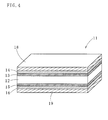
photovoltaic elements 11, and each of thephotovoltaic elements 11, as illustrated inFIG. 4 , is provided with a p-type amorphous silicon-basedthin film layer 14 on one face (upper face) of an n-type monocrystal silicon substrate (c-Si) 12 through an intrinsic amorphous silicon layer (i layer) 13, and an n-type amorphous silicon-basedthin film layer 16 on the other face (lower face) of the n-type monocrystal silicon substrate (c-Si) 12 through an intrinsic amorphous silicon layer (i layer) 15, and has a transparentconductive oxide layer 18 on top of the p-type amorphous silicon-basedthin film layer 14 and a transparentconductive oxide layer 19 underneath the n-type amorphous silicon-basedthin film layer 16. - As illustrated in
FIGS. 5(A) and 5(B) , the surface of each of the transparentconductive oxide layers finger electrodes 21 for gathering generated electrical power andbus bar electrodes 22 to be connected to the finger electrodes 21 (seePatent Literatures 1 and 2). The finger electrodes 21 (regular width is 50 to 100 µm, regular height is 50 µm or less) and the bus bar electrodes 22 (regular width is 0.5 to 2 mm, regular height is the same as that of the finger electrodes 21) are simultaneously formed by screen printing. The plurality ofphotovoltaic elements 11 are connected in series throughinterconnectors 25, heightening generated voltage of a photovoltaic apparatus as a whole. -
- Patent Literature 1: Japanese Unexamined Patent Application Publication No.
2005-317886 - Patent Literature 2: Japanese Unexamined Patent Application Publication No.
2012-054442 - The
finger electrodes 21 and thebus bar electrodes 22 each consist of silver paste which is a conductive adhesive. Silver paste, when having the same cross-sectional areas, has a larger electric resistance than regular metallic conductors (e.g., copper) and the like. On the other hand, since silver paste is non-translucent, when the widths of thefinger electrodes 21 and thebus bar electrodes 22 are increased, light-shielding rate increases and power generation efficiency decreases. - Therefore, cross-sectional areas have been acquired by repeating screen printing a plurality of times, however, there has been a problem in that in order to form a high-height power collecting member, a large amount of silver paste has become required, which has led to high cost of raw materials. Additionally, print accuracy of screen printing is low, and repeated printing at a same position gradually increases a width, which has led to another problem in that the
finger electrodes 21 have become formed with widths larger than necessary and light-shielding rate has increased.
Moreover, in order to connect the adjacentphotovoltaic elements 11, there has been a need to provide theinterconnectors 25 along thebus bar electrodes 22 aside from thebus bar electrodes 22. - The present invention has been made in view of the above circumstances, and an object thereof is to provide a photovoltaic apparatus that can be manufactured at a relatively low cost.
- In order to achieve the above object, according to a first aspect of the present invention, a photovoltaic apparatus includes: a plurality of photovoltaic elements each having transparent conductive oxide layers formed on the front and back thereof and generating electrical power by light irradiation; and power collecting members provided on the front and back of each of the photovoltaic elements. The photovoltaic apparatus further includes: finger electrodes provided to the power collecting members on the front sides, the finger electrodes being formed in parallel on top of the transparent conductive oxide layers on the front sides by gravure offset printing, the thickness of the finger electrodes being formed to be 5 µm or less; and a plurality of metallic conductor wires provided to the power collecting members on the front sides, the plurality of metallic conductor wires being joined to the finger electrodes in an orthogonal state, wherein the metallic conductor wires are extended further in one direction and joined to one of the power collecting members provided on the back sides of the adjoining photovoltaic elements to be connected in series.
- Since gravure offset printing is used for the formation of the finger electrodes, it becomes possible to print thin films, which is difficult to do by screen printing.
It is preferable for the thickness of the finger electrodes to be 1 µm or more, and when the thickness of the finger electrodes is less than 1 µm, it becomes difficult to actually produce them, and besides, electric resistance increases. Additionally, when the thickness of the finger electrodes increases, usage amount of metal paste (e.g., silver paste) increases, which increases the material cost. The width w of the finger electrodes is, for example, 40 to 200 µm (more preferably, 100 to 200 µm).
Moreover, it is preferable to use copper (including alloy) for the metallic conductor wires, however, other metallic wires (aluminum wires, silver wires, nickel wires and the like) can be used alternatively. - According to a second aspect of the present invention, in the photovoltaic apparatus of the first aspect of the present invention, the metallic conductor wires have a diameter d of 80 to 400 µm, and are arranged at a pitch of 15 d or more and 15 mm or less. Here, when the diameter d of the metallic conductor wires is smaller than 80 µm, electric resistance becomes large. It is possible for the diameter d of the metallic conductor wires to exceed 400 µm, however, electric resistance becomes smaller than necessary, and light-shielding rate becomes large at the same time. Additionally, metallic conductor wires (e.g., copper wires) having plating of dissimilar metals on the surfaces thereof can be used alternatively.
- According to a third aspect of the present invention, in the photovoltaic apparatuses of the first and the second aspects of the present invention, a low-melting-point metal (e.g., solder) is used for the joining of the metallic conductor wires and the finger electrodes. The low-melting-point metal in this case is formed on the metallic conductor wires by means of coating treatment, and it is preferable for the thickness of the low-melting-point metal to be approximately 0.05- to 0.2-fold of the diameter of the metallic conductor wires.
- In the photovoltaic apparatuses according to the first to third aspects of the present invention, by using a large number of metallic conductor wires as conventional bus bar electrodes, reduction in resistance can be achieved, and a photovoltaic apparatus having higher efficiency can be provided.
- In the case of the photovoltaic apparatuses according to the present invention, since the finger electrodes are formed by using gravure offset printing, the width of each finger electrode can be made substantially constant and the thickness can accurately be made thin, and what is more, since bus bar electrodes are eliminated and the metallic conductor wires are used instead, usage amount of the conductive adhesive (e.g., silver paste) has decreased, making it possible to manufacture a photovoltaic apparatus at a lower cost.
- Additionally, since the metallic conductor wires are extended further in one direction and joined to one of the power collecting members on the back sides of the adjoining photovoltaic elements, conventional interconnectors have become unnecessary, and assembling and manufacturing of a photovoltaic apparatus have become easier.
-
-
FIG. 1 is a plan view of a photovoltaic apparatus according to one embodiment of the present invention. -
FIG. 2 is a side view of the same photovoltaic apparatus. -
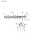
FIG. 3 is a cross-sectional view of A to A' inFIG. 1 . -
FIG. 4 is a schematic view of a photovoltaic element used for a photovoltaic apparatus according to a conventional example. -
FIGS. 5(A) and 5(B) are a plan view and a side view, respectively, of the same photovoltaic apparatus. - Next, with reference to the accompanying drawings, descriptions will be given on embodiments of the present invention. Components same as those of the photovoltaic apparatus according to the conventional example will be indicated by the same numerals.
As illustrated inFIGS. 1 ,2 and3 , aphotovoltaic apparatus 10 according to one embodiment of the present invention has a plurality ofphotovoltaic elements 11 to be connected in series. Each of thesephotovoltaic elements 11 is structured in the same way as the one illustrated inFIG. 4 (a heterojunction solar cell), and has an n-type monocrystal silicon substrate (c-Si) 12 in the middle, an intrinsicamorphous silicon layer 13 on top of the n-type monocrystal silicon substrate (c-Si) 12, an intrinsicamorphous silicon layer 15 underneath the n-type monocrystal silicon substrate (c-Si) 12, a p-type amorphous silicon-basedthin film layer 14 on the outer side of the intrinsicamorphous silicon layer 13, and an n-type amorphous silicon-basedthin film layer 16 on the outer side of the intrinsicamorphous silicon layer 15, and has a transparentconductive oxide layer 18 on the upper face and a transparentconductive oxide layer 19 on the lower face. - When light (e.g., sunlight) is irradiated to the surface of each of these
photovoltaic elements 11, potential differences occur between the transparent conductive oxide layers 18 and 19 on the front and back, and electrical power becomes generated. Electromotive force of a singlephotovoltaic element 11 is as small as approximately 0.7 V. Thus, the plurality ofphotovoltaic elements 11 are connected in series in order to obtain predetermined voltage. Since these structures are well known, detailed descriptions will be omitted. - On the front and back of each of the
photovoltaic elements 11, the transparent conductive oxide layers 18 and 19 are formed, and as illustrated inFIGS. 1 and2 , the surfaces of the transparent conductive oxide layers 18 and 19 include a plurality offinger electrodes 27 and a plurality ofmetallic conductor wires 28 put on the plurality offinger electrodes 27, thefinger electrodes 27 and themetallic conductor wires 28 are respectively arranged in parallel at equal intervals. In this embodiment, by the plurality offinger electrodes 27 composed of thin lines and the plurality ofmetallic conductor wires 28 arranged orthogonal to thefinger electrodes 27, the power collecting members on the front and back sides are formed. Each of the power collecting members on the front sides is electrically joined to each transparentconductive oxide layer 18 to be formed on the front side of each of thephotovoltaic elements 11. Each of the power collecting members on the back sides is electrically joined to each transparentconductive oxide layer 19 to be formed on the back side of each of thephotovoltaic elements 11. The power collecting members on the back sides can be different from those on the front sides. - Here, as illustrated in
FIG. 2 , thefinger electrodes 27 are formed by printing silver paste that is an example of metal pastes. The thickness (height) t of eachfinger electrode 27 is 1 µm or more and 5 µm or less, the width w thereof is 40 to 200 µm (more preferably, 100 to 200 µm, and even 50 to 150 µm), and each pitch p between thefinger electrodes 27 is approximately 10- to 20-fold of the width w. Thefinger electrodes 27 block out light, w/px100 (seeFIGS. 1 and2 ) expresses a function of light-shielding rate (%), and it is preferable for the light-shielding rate to be 10% or less. - When the cross-sectional area of each
finger electrodes 27 is made small, usage amount of silver paste decreases in proportion to the thickness, and it becomes possible to provide an inexpensive photovoltaic apparatus that requires smaller usage amount of silver paste. However, making the thickness extremely thin lowers fill factor (FF), therefore, it is desirable to determine the width w and the thickness t of thefinger electrodes 27 in such a manner that the fill factor does not become lowered too much. - In this case, in order to reduce the thickness t of the
finger electrodes 27, the technique of gravure offset printing (gravure printing) is used. Reducing the thickness t of thefinger electrodes 27 allows for a reduction in usage amount of silver paste at the time of manufacturing thephotovoltaic apparatus 10. - As illustrated in
FIG. 3 , on top of the plurality offinger electrodes 27 provided on the front side (and the back side) of eachphotovoltaic element 11 at small pitches, the plurality ofmetallic conductor wires 28 are arranged in parallel. The diameter d of thesemetallic conductor wires 28 is from 80 to 400 µm, and themetallic conductor wires 28 are wired at a pitch p1 of 15 d or more and 15 mm or less (e.g., pitches between themetallic conductor wires 28 are 4 mm). - Here, when the pitches between the
metallic conductor wires 28 become large, power collection areas of thefinger electrodes 27 become long and thephotovoltaic elements 11 become affected by resistance loss. When the pitches between themetallic conductor wires 28 become small, light-shielding rate increases. Therefore, in view of a balance between the two, it is preferable to design with the light-shielding rate of 5 to 10%. Also, themetallic conductor wires 28 and thefinger electrodes 27 are joined by a low-melting-point metal (e.g., solder) 30. - The low-melting-
point metal 30 is, as illustrated inFIG. 3 , with a predetermined thickness, preliminarily coated around themetallic conductor wires 28, and by melting the low-melting-point metal 30 through heating at a temperature of approximately 200°C, themetallic conductor wires 28 coated with the low-melting-point metal 30 become joined to thefinger electrodes 27. - The
metallic conductor wires 28 on the front sides of thephotovoltaic elements 11 are extended further in one direction, and joined to themetallic conductor wires 28 on the back sides of the adjoiningphotovoltaic elements 11. Here, the state of "being joined" includes the case where metallic conductor wires on the front sides of photovoltaic elements and on the back sides of adjoining photovoltaic elements are formed by a single metallic conductor wire, aside from the case where separate metallic conductor wires are connected to one another. - In this embodiment, unlike the conventional way, a conductive adhesive is not used for the power collecting members (i.e., bus bar electrodes), and the metallic conductor wires are used instead. Thus, bending becomes enabled, and interconnectors and the like become unnecessary, making the manufacturing easier.
- As described hereinbefore, the light-shielding rate in view of only the
finger electrodes 27 is (w/p)×100 (%). Also, when the diameter of themetallic conductor wires 28 is indicated by d, and the pitches between themetallic conductor wires 28 by p1, the light-shielding rate in view of thefinger electrodes 27 and themetallic conductor wires 28 is approximately {100(w/p)+100(d/p1)}%. It is preferable for the sum of these light-shielding rates to be 10% or less. Additionally, the cross-section of themetallic conductor wires 28 is circular. However, using metallic conductor wires having a rectangular cross-section, especially a longitudinal oblong cross-section allows for lowering of light-shielding rate while maintaining electric resistance. - Table 1 illustrates a working example performed to confirm the functions and effects of the present invention. No.1 to No. 7 each illustrate the cases where the height of finger electrodes is 0.1 µm, 0.3 µm, 0.5 µm, 1 µm, 3 µm, 5 µm and 10 µm. When the height of the finger electrodes is less than 1 µm, efficiency (η) also decreases, and it becomes hard to make the thickness less than 1 µm and constant even by the gravure offset printing.
On the other hand, when the thickness of the finger electrodes is further increased, usage amount of silver increases, which increases the manufacturing cost.[Table 1] Height of Finger Electrodes Isc/A Voc/V FF Rs/Ω η/% No.1 0.1 µm 9.031 0.724 0.732 6.20E-03 19.67 No.2 0.3 µm 9.032 0.723 0.743 5.51 E-03 19.94 No.3 0.5 µm 9.031 0.725 0.752 5.26E-03 20.23 No.4 1 µm 9.035 0.726 0.761 4.92E-03 20.51 No.5 3 µm 9.034 0.724 0.766 4.45E-03 20.59 No.6 5 µm 9.045 0.725 0.772 4.41 E-03 20.80 No.7 10 µm 9.038 0.726 0.781 4.30E-03 21.06 - The present invention is not limited to the above-described embodiment, and the structure thereof can be changed without altering the gist of the present invention. For example, in the above-described embodiment, copper wires are used as the metallic conductor wires, however, aluminum wires, nickel wires and the like can alternatively be used. Additionally, plating can be applied to the surfaces of the metallic conductor wires. Moreover, although silver paste is used as the conductive adhesive in producing of the finger electrodes, other conductive adhesives are usable as well.
- 10: photovoltaic apparatus, 11: photovoltaic element, 12: n-type monocrystal silicon substrate, 13: intrinsic amorphous silicon layer, 14: p-type amorphous silicon-based thin film layer, 15: intrinsic amorphous silicon layer, 16: n-type amorphous silicon-based thin film layer, 18, 19: transparent conductive oxide layer, 21: finger electrode, 22: bus bar electrode, 25: interconnector, 27: finger electrode, 28; metallic conductor wire, 30: low-melting-point metal
Claims (3)
- A photovoltaic apparatus, comprising:a plurality of photovoltaic elements each having transparent conductive oxide layers formed on the front and back thereof and generating electrical power by light irradiation; andpower collecting members provided on the front and back of each of the photovoltaic elements,the photovoltaic apparatus, further comprising:finger electrodes provided to the power collecting members on the front sides, the finger electrodes being formed in parallel on top of the transparent conductive oxide layers on the front sides by gravure offset printing, the thickness of the finger electrodes being formed to be 5 µm or less; anda plurality of metallic conductor wires provided to the power collecting members on the front sides, the metallic conductor wires being joined to the finger electrodes in an orthogonal state, whereinthe metallic conductor wires are extended further in one direction and joined to one of the power collecting members provided on the back sides of the adjoining photovoltaic elements to be connected in series.
- The photovoltaic apparatus according to claim 1, wherein
the metallic conductor wires have a diameter d of 80 to 400 µm, and are arranged at a pitch of 15 d or more and 15 mm or less. - The photovoltaic apparatus according to claim 1 or 2, wherein
a low-melting-point metal is used for the joining of the metallic conductor wires and the finger electrodes.
Applications Claiming Priority (2)
| Application Number | Priority Date | Filing Date | Title |
|---|---|---|---|
| JP2012255121A JP6050661B2 (en) | 2012-11-21 | 2012-11-21 | Photovoltaic generator manufacturing method |
| PCT/JP2013/081145 WO2014080894A1 (en) | 2012-11-21 | 2013-11-19 | Photovoltaic apparatus |
Publications (2)
| Publication Number | Publication Date |
|---|---|
| EP2924740A1 true EP2924740A1 (en) | 2015-09-30 |
| EP2924740A4 EP2924740A4 (en) | 2016-07-27 |
Family
ID=50776075
Family Applications (1)
| Application Number | Title | Priority Date | Filing Date |
|---|---|---|---|
| EP13856809.2A Withdrawn EP2924740A4 (en) | 2012-11-21 | 2013-11-19 | PHOTOVOLTAIC DEVICE |
Country Status (8)
| Country | Link |
|---|---|
| US (1) | US20160284895A1 (en) |
| EP (1) | EP2924740A4 (en) |
| JP (1) | JP6050661B2 (en) |
| KR (1) | KR20150088784A (en) |
| CN (1) | CN105027297A (en) |
| AU (1) | AU2013348851A1 (en) |
| TW (1) | TW201432929A (en) |
| WO (1) | WO2014080894A1 (en) |
Cited By (4)
| Publication number | Priority date | Publication date | Assignee | Title |
|---|---|---|---|---|
| EP2960946A3 (en) * | 2014-06-26 | 2016-04-06 | LG Electronics Inc. | Solar cell module |
| EP3171412A1 (en) * | 2015-11-17 | 2017-05-24 | LG Electronics Inc. | Apparatus and method for attaching interconnector of solar cell panel |
| EP3573113A1 (en) * | 2018-05-24 | 2019-11-27 | Solyco Technology GmbH | Photovoltaic module |
| EP4092759B1 (en) | 2014-09-30 | 2024-01-31 | Shangrao Xinyuan YueDong Technology Development Co. Ltd | Solar cell panel |
Families Citing this family (15)
| Publication number | Priority date | Publication date | Assignee | Title |
|---|---|---|---|---|
| JP2016027640A (en) * | 2014-06-30 | 2016-02-18 | 日東電工株式会社 | Solar battery module and sealing film therefor |
| KR102273014B1 (en) * | 2014-08-04 | 2021-07-06 | 엘지전자 주식회사 | Solar cell module |
| CN104282788B (en) * | 2014-09-28 | 2017-03-22 | 苏州中来光伏新材股份有限公司 | Main-grid-free high-efficiency back contact solar cell module, main-grid-free high-efficiency back contact solar cell assembly and manufacturing technology of main-grid-free high-efficiency back contact solar cell assembly |
| US20160126361A1 (en) | 2014-10-31 | 2016-05-05 | Byd Company Limited | Solar cell module and manufacturing method thereof |
| CN105576057B (en) * | 2014-10-31 | 2018-06-26 | 比亚迪股份有限公司 | Solar cell module and preparation method thereof |
| KR101889842B1 (en) | 2014-11-26 | 2018-08-20 | 엘지전자 주식회사 | Solar cell module |
| JP2018056145A (en) * | 2015-02-06 | 2018-04-05 | 長州産業株式会社 | Photovoltaic module |
| KR101739404B1 (en) * | 2015-08-07 | 2017-06-08 | 엘지전자 주식회사 | Solar cell panel |
| JP6692634B2 (en) * | 2015-12-01 | 2020-05-13 | 日本航空電子工業株式会社 | Touch panel |
| US10834815B2 (en) | 2015-12-01 | 2020-11-10 | Japan Aviation Electronics Industry, Limited | Printed wiring line, electronic device, touch panel, gravure plate, printed wiring line formation method, touch panel production method, and electronic device production method |
| KR102149926B1 (en) * | 2019-10-29 | 2020-08-31 | 엘지전자 주식회사 | Solar cell module |
| KR102266951B1 (en) * | 2019-10-29 | 2021-06-18 | 엘지전자 주식회사 | Solar cell module |
| CN116110980A (en) * | 2021-11-10 | 2023-05-12 | 浙江晶科能源有限公司 | A battery sheet and a photovoltaic module |
| KR102832575B1 (en) * | 2024-01-17 | 2025-07-11 | 주성엔지니어링(주) | Solar cell and method for manufacturing the same |
| JP2025158459A (en) * | 2024-04-04 | 2025-10-17 | トヨタ自動車株式会社 | Solar cell modules and interconnectors |
Family Cites Families (12)
| Publication number | Priority date | Publication date | Assignee | Title |
|---|---|---|---|---|
| US5151386A (en) * | 1990-08-01 | 1992-09-29 | Mobil Solar Energy Corporation | Method of applying metallized contacts to a solar cell |
| DE10239845C1 (en) * | 2002-08-29 | 2003-12-24 | Day4 Energy Inc | Electrode for photovoltaic cells, photovoltaic cell and photovoltaic module |
| US7122398B1 (en) * | 2004-03-25 | 2006-10-17 | Nanosolar, Inc. | Manufacturing of optoelectronic devices |
| JP4593980B2 (en) | 2004-03-29 | 2010-12-08 | 京セラ株式会社 | Photoelectric conversion device, solar cell element using the same, and solar cell module |
| JP4925598B2 (en) * | 2005-03-29 | 2012-04-25 | 京セラ株式会社 | Solar cell element and solar cell module using the same |
| WO2010030109A2 (en) * | 2008-09-12 | 2010-03-18 | 주식회사 엘지화학 | Front electrode for solar cell which minimizes power loss, and solar cell including the same |
| WO2011021655A1 (en) * | 2009-08-19 | 2011-02-24 | 三洋電機株式会社 | Solar battery, solar battery module and solar battery system |
| JP2011103356A (en) * | 2009-11-10 | 2011-05-26 | Mitsubishi Electric Corp | Solar cell electrode forming paste, solar cell, and method of manufacturing the same |
| JP2011142127A (en) * | 2009-12-11 | 2011-07-21 | Hitachi Chem Co Ltd | Solar cell structure and method of manufacturing the same |
| JP2012054442A (en) | 2010-09-02 | 2012-03-15 | Shin Etsu Chem Co Ltd | Method of manufacturing solar cell and screen plate making process for use therein |
| JP2012079869A (en) * | 2010-09-30 | 2012-04-19 | Fujifilm Corp | Organic thin-film solar cell |
| CN104321883A (en) * | 2011-12-13 | 2015-01-28 | 道康宁公司 | Photovoltaic cell and method of forming the same |
-
2012
- 2012-11-21 JP JP2012255121A patent/JP6050661B2/en active Active
-
2013
- 2013-11-19 TW TW102142041A patent/TW201432929A/en unknown
- 2013-11-19 KR KR1020157010951A patent/KR20150088784A/en not_active Withdrawn
- 2013-11-19 US US14/442,291 patent/US20160284895A1/en not_active Abandoned
- 2013-11-19 CN CN201380056524.6A patent/CN105027297A/en active Pending
- 2013-11-19 WO PCT/JP2013/081145 patent/WO2014080894A1/en not_active Ceased
- 2013-11-19 EP EP13856809.2A patent/EP2924740A4/en not_active Withdrawn
- 2013-11-19 AU AU2013348851A patent/AU2013348851A1/en not_active Abandoned
Cited By (10)
| Publication number | Priority date | Publication date | Assignee | Title |
|---|---|---|---|---|
| EP2960946A3 (en) * | 2014-06-26 | 2016-04-06 | LG Electronics Inc. | Solar cell module |
| US10164130B2 (en) | 2014-06-26 | 2018-12-25 | Lg Electronics Inc. | Solar cell module |
| US10170646B2 (en) | 2014-06-26 | 2019-01-01 | Lg Electronics Inc. | Solar cell module |
| US11201252B2 (en) | 2014-06-26 | 2021-12-14 | Lg Electronics Inc. | Solar cell module |
| US11522092B2 (en) | 2014-06-26 | 2022-12-06 | Shangrao Jinko Solar Technology Development Co., Ltd | Solar cell module |
| EP4092759B1 (en) | 2014-09-30 | 2024-01-31 | Shangrao Xinyuan YueDong Technology Development Co. Ltd | Solar cell panel |
| EP3171412A1 (en) * | 2015-11-17 | 2017-05-24 | LG Electronics Inc. | Apparatus and method for attaching interconnector of solar cell panel |
| US10586882B2 (en) | 2015-11-17 | 2020-03-10 | Lg Electronics Inc. | Solar cell panel, and apparatus and method for attaching interconnector of solar cell panel |
| US11152524B2 (en) | 2015-11-17 | 2021-10-19 | Lg Electronics Inc. | Solar cell panel, and apparatus and method for attaching interconnector of a solar cell panel |
| EP3573113A1 (en) * | 2018-05-24 | 2019-11-27 | Solyco Technology GmbH | Photovoltaic module |
Also Published As
| Publication number | Publication date |
|---|---|
| TW201432929A (en) | 2014-08-16 |
| CN105027297A (en) | 2015-11-04 |
| JP6050661B2 (en) | 2016-12-21 |
| JP2014103301A (en) | 2014-06-05 |
| WO2014080894A1 (en) | 2014-05-30 |
| US20160284895A1 (en) | 2016-09-29 |
| EP2924740A4 (en) | 2016-07-27 |
| AU2013348851A1 (en) | 2015-04-30 |
| KR20150088784A (en) | 2015-08-03 |
Similar Documents
| Publication | Publication Date | Title |
|---|---|---|
| US20160284895A1 (en) | Photovoltaic apparatus | |
| TWI689106B (en) | Solar cell and solar cell module | |
| TW201444103A (en) | Photovoltaic cell component with specific electrode architecture | |
| CN104282788A (en) | Main-grid-free high-efficiency back contact solar cell module, main-grid-free high-efficiency back contact solar cell assembly and manufacturing technology of main-grid-free high-efficiency back contact solar cell assembly | |
| WO2012043516A1 (en) | Solar-cell module and manufacturing method therefor | |
| CN104253169B (en) | Without main grid, high efficiency back contact solar cell module, assembly and preparation technology | |
| TW201624740A (en) | Solar cell with specific front surface electrode design | |
| CN104269462B (en) | Back contact solar cell back sheet without main grids, back contact solar cell assembly without main grids and manufacturing technology | |
| JP2017011312A (en) | Solar cell, solar cell module, method for manufacturing solar cell, and method for manufacturing solar cell module | |
| CN104269454B (en) | High-efficiency back contact solar cell back sheet without main grids, high-efficiency back contact solar cell assembly without main grids and manufacturing technology | |
| JP6217080B2 (en) | Solar cells | |
| TWI540742B (en) | Solar battery | |
| CN104319301A (en) | Main gate-free, high-efficiency and back-contact solar battery backplane, assembly and preparation process | |
| WO2012128284A1 (en) | Rear surface electrode-type solar cell, manufacturing method for rear surface electrode-type solar cell, and solar cell module | |
| WO2013094556A1 (en) | Solar cell with wiring sheet, solar cell module, and solar cell manufacturing method | |
| TW201607065A (en) | Solar cell module and solar cell module sealing film | |
| JP6455099B2 (en) | Solar cell unit and method for manufacturing solar cell unit | |
| JP6325925B2 (en) | Solar cell module and method for manufacturing solar cell module | |
| JP2014146697A (en) | Photovoltaic apparatus | |
| WO2016065942A1 (en) | Solar cell array, solar cell module and manufacturing methodthereof | |
| WO2016065953A1 (en) | Solar cell module and manufacturing method thereof |
Legal Events
| Date | Code | Title | Description |
|---|---|---|---|
| PUAI | Public reference made under article 153(3) epc to a published international application that has entered the european phase |
Free format text: ORIGINAL CODE: 0009012 |
|
| 17P | Request for examination filed |
Effective date: 20150516 |
|
| AK | Designated contracting states |
Kind code of ref document: A1 Designated state(s): AL AT BE BG CH CY CZ DE DK EE ES FI FR GB GR HR HU IE IS IT LI LT LU LV MC MK MT NL NO PL PT RO RS SE SI SK SM TR |
|
| AX | Request for extension of the european patent |
Extension state: BA ME |
|
| DAX | Request for extension of the european patent (deleted) | ||
| RA4 | Supplementary search report drawn up and despatched (corrected) |
Effective date: 20160628 |
|
| RIC1 | Information provided on ipc code assigned before grant |
Ipc: H01L 31/0747 20120101ALI20160622BHEP Ipc: H01L 31/05 20060101ALI20160622BHEP Ipc: H01L 31/0224 20060101AFI20160622BHEP |
|
| STAA | Information on the status of an ep patent application or granted ep patent |
Free format text: STATUS: THE APPLICATION IS DEEMED TO BE WITHDRAWN |
|
| 18D | Application deemed to be withdrawn |
Effective date: 20170126 |